L2044L汽车双路输出闪光器专用集成电路
具40VIN瞬态保护的微型模块LED串驱动器

献[l 5 . 1 的 调 节 时 间 大 大 缩 短 ; 稳 态 误 差 与 文 献【】 1q 63 1  ̄3 1 8 而 l
中 相 同 , 然 为 0 仍 。
s uai bsd n I cnrl 【 .Eet nc ein i l o ae o PD ot m tn o J ] l ri c o D s g
参考文献:
f
时j 目/
[】 1 刘冰 , 嵩 , 宁 , 基 于 PD 制 的 导 弹 分通 道 仿 真[. 高 何 等. I控 J电 】
子 设 计 工 程 ,0 9,7( 1 :7 9 . 2 0 l 1 )9 — 9
L U Bi ,GAO o g I n S n ,HE Ni g t a.Mis e s b c a n l n ,e 1 s i u ・h n e l
咨 询 编 号 : 0 01 01 2 1 1 4 1
-
1 7- 2
图 1 1 1 时 的 系 统 阶 跃 响 应 曲 线 0 3. S 2
F g 0 S e e p n e e l ft e c re t d s se o 312 i .1 t p r s o s u ̄e o o r c e y t m n 1 .s h
En ie r g 2 0 ,7( 1 :7 9 . gn ei , 0 91 1 )9 — 9 n
【】 杏 芳 , 瑞 熊 , 亚 男. 弹 飞 行 力 学【 . 京: 京理 工 2钱 林 赵 导 M】 北 北
4 结 论
本 文 先 参 考 相 关 文 献 建 立 了导 弹 纵 向 回 路 控 制 系 统 模 型 , 后 利 用 理 论 计 算 的方 法 设 计 了 PD控 制 器 参 数 . 着 然 I 接
EL2044C中文资料

Note : All information contained in this data sheet has been carefully checked and is believed to be accurate as of the date of publication; however, this data sheet cannot be a “controlled document”. Current revisions, if any, to these specifications are maintained at the factory and are available upon your request. We recommend checking the revision level before finalization of your design documentation.© 2001 Elantec Semiconductor, Inc.EL2044CGeneral DescriptionThe EL2044C is a high speed, low power, low cost monolithic opera-tional amplifier built on Elantec's proprietary complementary bipolar process. The EL2044C is unity-gain stable and features a 325V/µs slew rate and 120MHz gain-bandwidth product while requiring only 5.2 mA of supply current.The power supply operating range of the EL2044C is from ±18V down to as little as ±2V. For single-supply operation, the EL2044C operates from 36V down to as little as 2.5V. The excellent power sup-ply operating range of the EL2044C makes it an obvious choice for applications on a single +5V supply.The EL2044C also features an extremely wide output voltage swing of ±13.6V with V S = ±15V and R L = 1000Ω. At ±5V, output voltage swing is a wide ±3.8V with R L = 500Ω and ±3.2V with R L = 150Ω.Furthermore, for single-supply operation at +5V, output voltage swing is an excellent 0.3V to 3.8V with R L = 500Ω.At a gain of +1, the EL2044C has a -3dB bandwidth of 120MHz with a phase margin of 50°. It can drive unlimited load capacitance, and because of its conventional voltage-feedback topology, the EL2044C allows the use of reactive or non-linear elements in its feedback net-work. This versatility combined with low cost and 75mA of output-current drive makes the EL2044C an ideal choice for price-sensitive applications requiring low power and high speed.Connection DiagramDIP and SO PackageFeatures•120MHz -3dB bandwidth •Unity-gain stable •Low supply current = 5.2mA at V S = ±15V •Wide supply range= ±2V to ±18V dual-supply = 2.5V to 36V single-supply •High slew rate = 325V/µs•Fast settling = 80ns to 0.1% for a 10V step•Low differential gain = 0.04% at A V =+2, R L = 150Ω•Low differential phase = 0.15° at A V = +2, R L = 150Ω•Stable with unlimited capacitive load•Wide output voltage swing = ±13.6V with V S = ±15V, R L = 1000Ω= 3.8V/0.3V with V S = +5V,R L = 500Ω•Low cost, enhanced replacement for the AD847 and LM6361Applications•Video amplifier•Single-supply amplifier •Active filters/integrators •High-speed sample-and-hold •High-speed signal processing •ADC/DAC buffer •Pulse/RF amplifier •Pin diode receiver •Log amplifier•Photo multiplier amplifier •Difference amplifierOrdering InformationPart No.Temp. Range Package Outline #EL2044CN -40°C to +85°C 8-Pin P-DIP MDP0031EL2044CS-40°C to +85°C8-Lead SOMDP0027EL2044CLow Power/Low Voltage 120MHz Unity-Gain Stable Operational AmplifierSeptember 26, 20012EL2044CLow Power/Low Voltage 120MHz Unity-Gain Stable Operational AmplifierE L 2044CAbsolute Maximum Ratings (T A= 25°C)Supply Voltage (V S )±18V or 36VPeak Output Current (I OP )Short-Circuit ProtectedOutput Short-Circuit DurationInfinite(A heat-sink is required to keep junction temperature below absolute maximum when an output is shorted.)Input Voltage (V IN)±V S Differential Input Voltage (dV IN )±10VPower Dissipation (P D )See Curves Operating Temperature Range (T A )-40°C to +85°C Operating Junction Temperature (T J )150°CStorage Temperature (T ST )-65°C to +150°CImportant Note:All parameters having Min/Max specifications are guaranteed. Typ values are for information purposes only. Unless otherwise noted, all tests are at the specified temperature and are pulsed tests, therefore: T J = T C = T A .DC Electrical CharacteristicsV S = ±15V, R L = 1000Ω, unless otherwise specified Parameter Description ConditionTemp Min Typ Max Unit V OS Input Offset Voltage V S = ±15V 25°C 0.57.0mV T MIN , T MAX13.0mV TCV OS Average Offset (Note 2)All 10.0µV/°CVoltage Drift I BInput Bias Current V S = ±15V 25°C 2.88.2µA T MIN , T MAX11.2µA V S = ±5V25°C 2.8µA I OSInput Offset Current V S = ±15V 25°C 50300nA T MIN , T MAX500nA V S = ±5V25°C 50nA TCI OS Average Offset Current Drift [1]All 0.3nA/°C A VOLOpen-Loop GainV S = ±15V,V OUT = ±10V, R L = 1000Ω25°C 8001500V/V T MIN , T MAX600V/V V S = ±5V, V OUT = ±2.5V, R L = 500Ω25°C 1200V/V V S = ±5V, V OUT = ±2.5V, R L = 150Ω25°C 1000V/V PSRR Power Supply Rejection Ratio V S = ±5V to ±15V 25°C 6580dB T MIN , T MAX60dB CMRR Common-Mode Rejection Ratio V CM = ±12V, V OUT = 0V 25°C 7090dB T MIN , T MAX70dB CMIRCommon-Mode Input Range V S = ±15V 25°C ±14.0V V S = ±5V 25°C ±4.2V V S = +5V25°C 4.2/0.1V V OUT Output Voltage SwingV S = ±15V, R L = 1000Ω25°C ±13.4±13.6V T MIN , T MAX±13.1V V S = ±15V, R L = 500Ω25°C ±12.0±13.4V V S = ±5V, R L = 500Ω25°C ±3.4±3.8V V S = ±5V, R L = 150Ω25°C ±3.2V V S = +5V, R L = 500Ω25°C 3.6/0.4 3.8/0.3V T MIN , T MAX3.5/0.5V I SCOutput Short Circuit Current25°C 4075mA T MIN , T MAX35mA3EL2044CLow Power/Low Voltage 120MHz Unity-Gain Stable Operational AmplifierEL2044CI SSupply CurrentV S = ±15V, No Load 25°C 5.27mA T MIN , T MAX7.6mA V S = ±5V, No Load25°C 5.0mA R IN Input Resistance Differential 25°C 150k ΩCommon-Mode 25°C 15M ΩC IN Input Capacitance A V = +1@ 10MHz 25°C 1.0pF R OUT Output Resistance A V = +125°C 50m ΩPSORPower-Supply Operating RangeDual-Supply 25°C ±2.0±18.0V Single-Supply25°C2.536.0V1.Measured from T MIN to T MAX .DC Electrical Characteristics (Continued)V S = ±15V, R L = 1000Ω, unless otherwise specified Parameter Description ConditionTemp MinTyp Max Unit4EL2044CLow Power/Low Voltage 120MHz Unity-Gain Stable Operational AmplifierE L 2044CClosed-Loop AC Electrical CharacteristicsV S = ±15V, A V = +1, R L = 1000¾ unless otherwise specified Parameter DescriptionConditionTemp Min Typ Max Unit BW-3 dB Bandwidth (V OUT = 0.4 V PP )V S = ±15V, A V = +125°C 120MHz V S = ±15V, A V = -125°C 60MHz V S = ±15V, A V = +225°C 60MHz V S = ±15V, A V = +525°C 12MHz V S = ±15V, A V = +1025°C 6MHz V S = ±5V, A V = +125°C 80MHz GBWP Gain-Bandwidth Product V S = ±15V 25°C 60MHz V S = ±5V25°C 45MHz PM Phase Margin R L = 1 k Ω, C L = 10 pF 25°C 50°SR Slew Rate[1]V S = ±15V, R L = 1000Ω25°C 250325V/µs V S = ±5V, R L = 500Ω25°C 200V/µs FPBW Full-Power Bandwidth [2]V S = ±15V 25°C 4.05.2MHz V S = ±5V 25°C 12.7MHz t r , t f Rise Time, Fall Time 0.1V Step 25°C 3.0ns OS Overshoot 0.1V Step25°C 20%t PD Propagation Delay 25°C 2.5ns t s Settling to +0.1%(A V = +1)V S = ±15V, 10V Step 25°C 80ns V S = ±5V, 5V Step 60ns dG Differential Gain [3]NTSC/PAL 25°C 0.04%dP Differential Phase (Note 5)NTSC/PAL 25°C 0.15°eN Input Noise Voltage 10kHz 25°C 15.0nV/√Hz iN Input Noise Current 10kHz 25°C 1.50pA/√Hz CI STABLoad Capacitance StabilityA V = +125°CInfinitepF1.Slew rate is measured on rising edge.2.For V S = ±15V, V OUT = 20V PP . For V S = ±5V, V OUT = 5V PP . Full-power bandwidth is based on slew rate measurement using: FPBW = SR/(2π *Vpeak).3.Video Performance measured at V S = ±15V, A V = +2 with 2 times normal video level across R L = 150Ω. This corresponds to standard video levelsacross a back-terminated 75Ω load. For other values of R L , see curves.5EL2044CLow Power/Low Voltage 120MHz Unity-Gain Stable Operational AmplifierEL2044CTypical Performance CurvesNon-InvertingFrequency ResponseInverting Frequency ResponseFrequency Response for Various Load ResistancesEquivalent Input NoiseSettling Time vsOutput Voltage ChangeOutput Voltage Range vs Supply VoltageCommon-Mode Input Range vs Supply Voltage Supply Current vs Supply Voltage CMRR, PSRR and Closed-Loop Output Resistance vs FrequencyOpen-Loop Gain and Phase vs Frequency Output Voltage Swing vs Frequency2nd and 3rd Harmonic Distortion vs Frequency6EL2044CLow Power/Low Voltage 120MHz Unity-Gain Stable Operational AmplifierE L 2044CGain-Bandwidth Product vs Supply Voltage Open-Loop Gain vs Supply Voltage Slew-Rate vs Supply VoltageVoltage Swingvs Load ResistanceOpen-Loop Gain vs Load Resistance Bias and Offset Current vs Input Common-Mode VoltageOffset Voltage vs Temperature Bias and OffsetCurrent vs Temperature Supply Current vs TemperatureOpen-Loop Gain PSRR and CMRR vs Temperature Slew Rate vs TemperatureGain-Bandwidth Product vs Temperature7EL2044CLow Power/Low Voltage 120MHz Unity-Gain Stable Operational AmplifierEL2044CShort-Circuit Current vs Temperature Gain-Bandwidth Product vs Load Capacitance Overshoot vsLoad CapacitanceSmall-Signal Step Response Short-Circuit Current Large-SignalDifferential Gain and Phase vs DC Input Offset at 3.58MHz Differential Gain and Phase vs DC Input Offset at 4.43MHz Differential Gain and Phase vs Number of 150Ω Loads at 3.58MHz8-Lead SO Maximum Power Dissipation vs Ambient Temperature8-Pin Plastic DIP Maximum Power Dissipation vs Ambient Temperature Differential Gain and Phase vs Number of 150Ω Loads at 4.43MHz8EL2044CLow Power/Low Voltage 120MHz Unity-Gain Stable Operational AmplifierE L 2044CSimplified SchematicBurn-In CircuitAll Packages Use the Same SchematicEL2044C Low Power/Low Voltage 120MHz Unity-Gain Stable Operational Amplifier EL2044C Applications InformationProduct DescriptionThe EL2044C is a low-power wideband monolithic operational amplifier built on Elantec's proprietary high-speed complementary bipolar process. The EL2044C uses a classical voltage-feedback topology which allows it to be used in a variety of applications where current-feedback amplifiers are not appropriate because of restrictions placed upon the feedback element used with the amplifier. The conventional topology of the EL2044C allows, for example, a capacitor to be placed in the feedback path, making it an excellent choice for applications such as active filters, sample-and-holds, or integrators. Similarly, because of the ability to use diodes in the feedback network, the EL2044C is an excellent choice for applications such as fast log amplifiers.Single-Supply OperationThe EL2044C has been designed to have a wide input and output voltage range. This design also makes the EL2044C an excellent choice for single-supply opera-tion. Using a single positive supply, the lower input voltage range is within 100mV of ground (R L = 500Ω), and the lower output voltage range is within 300mV of ground. Upper input voltage range reaches 4.2V, and output voltage range reaches 3.8V with a 5V supply and R L = 500Ω. This results in a 3.5V output swing on a sin-gle 5V supply. This wide output voltage range also allows single-supply operation with a supply voltage as high as 36V or as low as 2.5V. On a single 2.5V supply, the EL2044C still has 1V of output swing.Gain-Bandwidth Product and the -3dB BandwidthThe EL2044C has a gain-bandwidth product of 60MHz while using only 5.2mA of supply current. For gains greater than 4, its closed-loop -3dB bandwidth is approximately equal to the gain-bandwidth product divided by the noise gain of the circuit. For gains less than 4, higher-order poles in the amplifier's transfer function contribute to even higher closed loop band-widths. For example, the EL2044C has a -3dB bandwidth of 120MHz at a gain of +1, dropping to60MHz at a gain of +2. It is important to note that the EL2044C has been designed so that this “extra” band-width in low-gain applications does not come at the expense of stability. As seen in the typical performance curves, the EL2044C in a gain of +1 only exhibits 1.0dB of peaking with a 1000Ω load.Video PerformanceAn industry-standard method of measuring the video distortion of a component such as the EL2044C is to measure the amount of differential gain (dG) and differ-ential phase (dP) that it introduces. To make these measurements, a 0.286V PP (40 IRE) signal is applied to the device with 0V DC offset (0 IRE) at either 3.58MHz for NTSC or 4.43MHz for PAL. A second measurement is then made at 0.714V DC offset (100 IRE). Differential gain is a measure of the change in amplitude of the sine wave, and is measured in percent. Differential phase is a measure of the change in phase, and is measured in degrees.For signal transmission and distribution, a back-termi-nated cable (75Ω in series at the drive end, and 75Ω to ground at the receiving end) is preferred since the impedance match at both ends will absorb any reflec-tions. However, when double termination is used, the received signal is halved; therefore a gain of 2 configu-ration is typically used to compensate for the attenuation.The EL2044C has been designed as an economical solu-tion for applications requiring low video distortion. It has been thoroughly characterized for video perfor-mance in the topology described above, and the results have been included as typical dG and dP specifications and as typical performance curves. In a gain of +2, driv-ing 150¾, with standard video test levels at the input, the EL2044C exhibits dG and dP of only 0.04% and 0.15° at NTSC and PAL. Because dG and dP can vary with dif-ferent DC offsets, the video performance of the EL2044C has been characterized over the entire DC off-set range from -0.714V to +0.714V. For more information, refer to the curves of dG and dP vs DC Input Offset.910EL2044CLow Power/Low Voltage 120MHz Unity-Gain Stable Operational AmplifierE L 2044CThe output drive capability of the EL2044C allows it to drive up to 2 back-terminated loads with good video per-formance. For more demanding applications such as greater output drive or better video distortion, a number of alternatives such as the EL2120C, EL400C, or EL2073C should be considered.Output Drive CapabilityThe EL2044C has been designed to drive low imped-ance loads. It can easily drive 6V PP into a 150Ω load.This high output drive capability makes the EL2044C an ideal choice for RF, IF and video applications. Further-more, the current drive of the EL2044C remains a minimum of 35mA at low temperatures. The EL2044C is current-limited at the output, allowing it to withstand shorts to ground. However, power dissipation with the output shorted can be in excess of the power-dissipation capabilities of the package.Capacitive LoadsFor ease of use, the EL2044C has been designed to drive any capacitive load. However, the EL2044C remains stable by automatically reducing its gain-bandwidth product as capacitive load increases. Therefore, for max-imum bandwidth, capacitive loads should be reduced as much as possible or isolated via a series output resistor (R S ). Similarly, coax lines can be driven, but best AC performance is obtained when they are terminated with their characteristic impedance so that the capacitance of the coaxial cable will not add to the capacitive load seen by the amplifier. Although stable with all capacitive loads, some peaking still occurs as load capacitance increases. A series resistor at the output of the EL2044C can be used to reduce this peaking and further improve stability.Printed-Circuit LayoutThe EL2044C is well behaved, and easy to apply in most applications. However, a few simple techniques will help assure rapid, high quality results. As with any high-frequency device, good PCB layout is necessary for optimum performance. Ground-plane construction is highly recommended, as is good power supply bypass-ing. A 0.1µF ceramic capacitor is recommended for bypassing both supplies. Lead lengths should be as short as possible, and bypass capacitors should be as close tothe device pins as possible. For good AC performance,parasitic capacitances should be kept to a minimum at both inputs and at the output. Resistor values should be kept under 5k Ω because of the RC time constants associ-ated with the parasitic capacitance. Metal-film and carbon resistors are both acceptable, use of wire-wound resistors is not recommended because of their parasitic inductance. Similarly, capacitors should be low-induc-tance for best performance.The EL2044C MacromodelThis macromodel has been developed to assist the user in simulating the EL2044C with surrounding circuitry. It has been developed for the PSPICE simulator (copywrit-ten by the Microsim Corporation), and may need to be rearranged for other simulators. It approximates DC,AC, and transient response for resistive loads, but does not accurately model capacitive loading. This model is slightly more complicated than the models used for low-frequency op-amps, but it is much more accurate for AC analysis.The model does not simulate these characteristics accurately:noise non-linearities settling-time temperature effects CMRR PSRRmanufacturing variationsEL2044C Low Power/Low Voltage 120MHz Unity-Gain Stable Operational Amplifier EL2044C EL2044C MacromodelIN+IN+IN+IN+IN+IN+NININININ* Connections: +input* | -input* | | +Vsupply* | | | -Vsupply* | | | | output* | | | | |.subckt M2044 3 2 7 4 6** Input stage*ie 7 37 1mAr6 36 37 800r7 38 37 800rc1 4 30 850rc2 4 39 850q1 30 3 36 qpq2 39 2 38 qpaediff 33 0 39 30 1.0rdiff 33 0 1Meg** Compensation Section*ga 0 34 33 0 1mrh 34 0 2Megch 34 0 1.3pFrc 34 40 1Kcc 40 0 1pF** Poles*ep 41 0 40 0 1rpa 41 42 200cpa 42 0 1pFrpb 42 43 200cpb 43 0 1pF** Output Stage*ios1 7 50 1.0mAios2 51 4 1.0mAq3 4 43 50 qpq4 7 43 51 qnq5 7 50 52 qnq6 4 51 53 qpros1 52 6 25ros2 6 53 25** Power Supply Current*ips 7 4 2.7mA*IN+IN+IN+IN+IN+IN+NININININ* Models*.model qn npn(is=800E-18 bf=200 tf=0.2nS).model qpa pnp(is=864E-18 bf=100 tf=0.2nS).model qp pnp(is=800E-18 bf=125 tf=0.2nS).ends1112EL2044CLow Power/Low Voltage 120MHz Unity-Gain Stable Operational AmplifierE L 2044CEL2044C Macromodel13EL2044CLow Power/Low Voltage 120MHz Unity-Gain Stable Operational AmplifierE L 2044CGeneral DisclaimerSpecifications contained in this data sheet are in effect as of the publication date shown. Elantec, Inc. reserves the right to make changes in the cir-cuitry or specifications contained herein at any time without notice. Elantec, Inc. assumes no responsibility for the use of any circuits described herein and makes no representations that they are free from patent infringement.WARNING - Life Support PolicyElantec, Inc. products are not authorized for and should not be used within Life Support Systems without the specific written consent of Elantec, Inc. Life Support systems are equipment intended to sup-port or sustain life and whose failure to perform when properly used in accordance with instructions provided can be reasonably expected to result in significant personal injury or death. Users con-templating application of Elantec, Inc. Products in Life Support Systems are requested to contact Elantec, Inc. factory headquarters to establish suitable terms & conditions for these applications. Elan-tec, Inc.’s warranty is limited to replacement of defective components and does not cover injury to persons or property or other consequential damages.S e p t e m b e r 26, 2001Printed in U.S.A.Elantec Semiconductor, Inc.675 Trade Zone pitas, CA 95035Telephone:(408) 945-1323(888) ELANTECFax:(408) 945-9305European Office:+44-118-977-6020Japan Technical Center: +81-45-682-5820。
闪光器控制集成电路L2044

闪光器控制集成电路L2044.txt*一篇一篇的翻着以前的的签名,那时候的签名有多幼稚就有多么的幼稚。
你连让我报复的资格都没有-〞好想某天来电显示是你的号码。
好想某天你的状态是为我而写。
有些人,我们明知道是爱的,也要去放弃,因为没结局产品名称:闪光器控制集成电路L2044产品介绍:品牌 KD 型号 L2044批号 L2044 封装以封装营销方式厂家直销产品性质热销处理信号模拟信号制作工艺半导体集成导电类型双极型集成程度中规模规格尺寸 DIP14和SO14(mm)工作温度 -40~100(℃)静态功耗 10uA(mW)一、概述集成电路L2044 被应用于继电器控制的汽车闪光器控制电路中。
汽车的两边由两个输出平台分别控制。
汽车左边和右边的定向输入中只有很小的控制电流,这使得开关可以带小负载运行。
独立的报警信号输入使得控制报警的开关线路变得简单。
在定向模式下,当灯泡出故障时,闪光频率倍增。
由于L2044 的电流消耗极低,它可以直接与电源相连接。
二、特性◇闪光频率具有温度和电压补偿◇极低的电流消耗,< 10μA(开关断开)◇车灯失效时倍闪报警◇电源反接保护◇双继电器输出驱动电流大,饱和电压低◇三个控制输入:左向、右向以及报警◇最小车灯负载功率1W ◇抗电磁干扰能力强三、功能描述◆振荡器(管脚1、管脚14)闪光频率f1由R1C1 组成的以下公式决定(见图2):f1 ≈Hz其中C1≤ 47μF R1=6.8kΩ~180kΩ其中灯泡有故障时,①振荡器频率变为故障频率f2,f2 ≈ 2.2 f1,②正常频闪状态占空比为50%,③灯泡故障时占空比40%◆左、右向的启动输入(管脚2、管脚3)当输入比较器接地时(下接电阻器R7 或R5),闪光器不工作。
闪光器左右定向开关闭合时会使比较器状态发生改变并且使引脚11 和引脚13 处的输出端动作。
R6 和R4 是输入端的保护电阻。
当闪光器开关断开时,电流消耗仅为I<10μA。
GEC1041B规格书(原位替换Atmel1041、LD1041、UAA1041、LD4761)
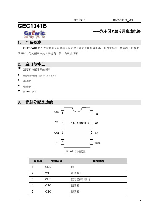
3. 管脚分配及功能
GND 1
8 SI
VS 2 7 GEC1041B LD
OUT 3
6 IEN
OSC 4
5 OSC1
图 3-1 引脚配置
管脚名
管脚符号
1
GND
2
VS
3
OUT
4
OSC
5
OSC1
功能描述 地 电源电压 继电器控制输出 振荡器 振荡器
3
6
IEN
7
LD
8
SI
过流保护配置 灯故障检测 启动输入
73
155
45 35 63 70 83 —
—
-40
DATASHEET_V2.0
典型 最大 单位
12
16
V
20.2
21.5
V
-
1.5
V
150
200
50
80
mA
120
200 mA
10
100
μA
85
97
次/ 分
185
210
50
55
%
40
45
%
71
mV
80
91
0.64
—
S
—
0.2
S
85
℃
5
5. 应用实例
12V 闪光器应用电路 R1=220KΩ R2=3.3KΩ R3=220Ω Rs*=0.03Ω C1=2.2μf Rj、S1 为继电器,线圈电阻 Rj-100Ω
Rj = 100Ω
IOL
引线 4=GND
引线 7=Vcc
R1=220KΩ
f1
C1=2.2μf
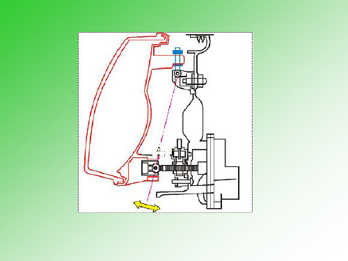
汽车闪光器结构图工作原理
二、电容式闪光器
• 它主要是由一个继电器和一个电容器组成。在 继电器的铁心6上绕有串联线圈3和并联线圈4, 电容器7采用大容量的电解电容器(约1500μF)。
• 电容式闪光器是利用电容器充、放电延时特性, 使继电器的两个线圈产生的电磁吸力时而相加, 时而相减,继电器便产生周期的开关动作,从 而使转向信号灯闪烁。
• (1)汽车转向时,接通 转向灯开关6,蓄电他即 向转向信号灯供电,电流 由蓄电池正极→接线柱 B→支架1→叶片2→热胀 条3→动触点4→静触点 5→支架8→接线柱L→转 向灯开关6→转向信号灯9 和指示灯7→搭铁→蓄电 池负极,形成回路,转向 信号灯9立即发亮。
(3)经过一段较短时间后,镍铬 丝受热膨胀而伸长,使触点3、4闭 合。触点闭合后,电流由蓄电池正 极→接线柱7→活动触点臂→触点4、 3→线圈2→接线柱8→转向开关9→ 右(前、后)转向情号灯13和右转向 指示灯12→搭铁→蓄电池负极,形 成回路。此时由于附加电阻6和镍 铬丝5被短路,而线圈2中有电流通 过产生电磁吸力使触点3、4闭合更 为紧密,线路中的电阻小,电流大, 故转向灯发出较亮的光。 (4)但镍铬丝因被短路逐渐冷却 而收缩,又打开触点3、4,防加电 阻又重新串入电路,灯光又变暗。 如此反复变化,触点时开时闭,附 加电阻交替地被接入或短路,使通 过转向信号灯的电流忽大忽小,从 而使转向信号灯一明一暗地闪烁, 标示车辆行驶的方向。
(或更换新前照灯总成)时,应进行调 整。
转向信号灯电路的组成
1、转向信号灯电路主要由转向信号 灯、闪光器和转向灯开关等组成。
2、转向信号灯的闪烁是由闪光器控 制的。
常见闪光器类型
1、电热式 2、电容式 3、电子式 4、水银式
一、电热丝式闪光器
各种LED驱动芯片

意法半导体(ST)推出一款驱动电流高达80mA的24在一个7x7mm的TQFP48封装内,新产品效能相当于三个普通的8路输出驱动器。
STP24DP05内置SPI端口提供精确的控制诊断功能。
ST公司的STP24DP05是带输出误差检测的24位移位寄存器恒流LED驱动器,包含有8x3位串进并出的移位寄存器,输出级有24个可调整的电流源,提供5-80mA恒定电流来驱动LED.电源电压可低到3V,输出电压可高达20V,主要应用在LCD屏显示器.本文介绍了STP24DP05的主要特性, 方框图和典型应用电路图.STP24DP05 24-bit constant current LED sink driver with output error detectionThe STP24DP05 is a monolithic, low voltage, low current power 24-bit shift register designed for LED pan EL displays. The device contains a 8 x 3-bit serial-in, parallel-out shift register that feeds a 8 x 3-bit D-type storage register. In the output stage, twenty-four regulated current sources were designed to provide 5-80 mA constant current to drive the LEDs.The 8x3 shift registers data flow sequence order can be managed with two dedicated pins. The STP24DP05 has a dedicated pin to activate the outputs with a sequential delay, that will prevent inrush current during outputs turn-ON.The device detection circuit checks 3 different conditions that can occur on the output line: short to GND, short to VO or open line.The data detection results are loaded in the shift registers and shifted out via the serial line output. The detection functionality is activated with a dedicated pin or as alternative, through a logic sequence that allows the user to enter or exit from detection mode.Through three external resistors, users can adjust the output current for each 8-channel group, controlling in this way the light intensity of LEDs. The STP24DP05 guarantees a 20 V output driving capability, allowing users to connect more LEDs in series.The high clock frequency, 25 MHz, makes the device suitable for high data rate transmission.The 3.3 V of voltage supply is useful for applications that interface any micro from 3.3 V.主要特性:■Low voltage power supply down to 3 V■8 x 3 constant current output channels■Adjustable output current through external resistors■Short and open output error detection■Serial data IN/Parallel data OUT■Shift register data flow registers control■Accepts 3.3 V and 5 V micro driver■Output current: 5-80 mA■25 MHz clock frequency■High thermal efficiency packageM3354/LM2792电荷泵驱动白光LED的电路发布商:NS 2007年12月13日美国国家半导体公司开发了许多用来驱动白光LED的解决方案,其中包括交换式电容变换器方案和采用电感器的交换式稳压器方案。
汽车转向信号闪光器
信号。
2.3 SG167型集成电路闪光器
由于电子技术的不断发展, 转向闪光器的结构
原理已由集成电路式闪光器替代了晶体管式闪光
器。常用进口集成电路有U2043B、UAA1041、L9686
等型号, 这些都是专用集成电路, 近年来国产的专
用集成电路已研制比较成熟, 型号种类很多, 如
LZ1041、 LD7208、 BU1041、 LT1041 等 , 现 以 天 津
设计●研究
De s ign●Re s e a rch
汽车转向信号闪光器
刘玉武 ( 天津市鹏程汽车配件厂, 天津 300113)
摘要: 简单介绍汽车用闪光器种类及构成原理, 详细阐述天津市鹏程汽车配件厂生产的几种闪光器的工作原理 及特点。
关键词: 闪光器; 晶体管; 集成电路 中图分类号: U463.654 文献标识码: A 文章编号: 1003- 8639( 2007) 08- 0008- 03
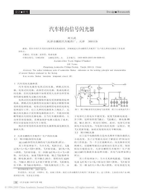
图6 SGD172型双继电器闪光器电气原理图 ( 用于天津一汽威乐轿车、东南汽车商务车)
该电路的特点是有2个继电器, 图6中J1、J2分别 为2个 继 电 器 的 常 开 触 点 , K是 电 源 总 开 关 , 由IG 引 出 , 通 过 5 A熔 断 器 接 至 1 端 , 2、 3 端 分 别 接 LR ( 右) 、LL ( 左) 闪光灯。电源B+通过10 A熔断器连 接4端, 5、6端分别通过开关K2搭铁, 7端GND是搭 铁端, 8端通过开关K1搭铁。该电路的控制原理是 : 总电源开关K接通后, 当开关K2接通5端搭铁, 电路 中 继 电 器J1动 作 与 释 放 , 其 触 点J1接 通 与 断 开 , LL 左 边 闪 光 灯 正 常 闪 烁 。 同 理 , 当 开 关K2接 通6端 搭 铁时, 电路中继电器J2动作与释放, LR右 边 闪 光 灯 正 常 闪 烁 。 当 开 关K1将8端 搭 铁 时 , J1和J2 2个 继 电 器同时工作, 此时即为双闪状态。该电路也具有主 灯断丝后快闪报警功能, 其原理与前述相同。
汽车上闪光继电器的原理全

汽车上闪光继电器的原理全解2023-10-27•闪光继电器概述•闪光继电器的工作原理•闪光继电器的类型与规格•闪光继电器的选用与安装•闪光继电器的故障诊断与排除目•未来发展趋势与新技术应用录01闪光继电器概述定义闪光继电器是一种控制开关,用于控制汽车的转向信号灯或其他外部灯具。
作用通过接收来自汽车控制系统的信号,控制闪光继电器触点的开关状态,从而实现转向信号灯或其他外部灯具的闪烁或常亮。
定义与作用工作电压闪光继电器的工作电压通常为12V或24V,根据车型和系统需求而定。
线圈与触点闪光继电器通常由一个线圈和一对或多个触点组成。
当线圈通电时,磁场产生,触点闭合;当线圈断电时,磁场消失,触点断开。
闪烁与常亮通过控制闪光继电器的线圈的开关状态,可以实现转向信号灯或其他外部灯具的闪烁或常亮。
当线圈持续通电时,触点持续闭合,灯具持续亮起;当线圈断电时,触点断开,灯具熄灭。
通过交替通电断电,实现灯具的闪烁效果。
汽车转弯01当汽车转弯时,控制系统会检测到转向信号,并向闪光继电器发送信号。
闪光继电器根据信号控制触点的开关状态,从而实现转向信号灯的闪烁。
危险报警02在一些特殊情况下,如汽车被盗或遇到危险时,驾驶员可以手动触发危险报警系统。
此时,闪光继电器控制转向信号灯和其他外部灯具以高频闪烁,以引起周围人的注意。
其他应用03除了控制转向信号灯外,闪光继电器还可以用于控制其他外部灯具,如制动灯、倒车灯等。
02闪光继电器的工作原理当有电流通过时,会产生磁场,使铁芯吸合。
线圈触点弹簧由铁芯和触点组成,当铁芯吸合时,触点闭合,电路接通。
当铁芯吸合后,弹簧会拉回铁芯,使触点断开。
03闪光继电器的组成0201电源通过两个触点控制转向灯的闪烁。
闪光继电器连接到闪光继电器的输出端。
转向灯闪光继电器的电路图解析通过点火开关连接到蓄电池。
闪光继电器的动作过程当点火开关打开时,电流通过点火开关和闪光继电器的线圈,产生磁场并吸合铁芯。
铁芯吸合后,触点闭合,电流通过转向灯并使其亮起。
- 1、下载文档前请自行甄别文档内容的完整性,平台不提供额外的编辑、内容补充、找答案等附加服务。
- 2、"仅部分预览"的文档,不可在线预览部分如存在完整性等问题,可反馈申请退款(可完整预览的文档不适用该条件!)。
- 3、如文档侵犯您的权益,请联系客服反馈,我们会尽快为您处理(人工客服工作时间:9:00-18:30)。
丹 http://东w华ww奥.h电uaa子oe有.c限om公司
丹 http://东w华ww奥.h电uaa子oe有.c限om公司
丹东华奥电子有限公司
Automobile Semiconductor
17/134
201109
共6页 第3页
返回目录
丹 http://东w华ww奥.h电uaa子oe有.c限om公司
相连接。外部元件稍加改动,可用于 24V 闪光器,也可以用于控制 LED 车灯。
DIP14
特点
● 闪光频率具有温度和电压补偿 ●车灯失效时倍闪报警
●极低的电流消耗,< 10µA(开关断开) ●电源反接保护
●双继电器输出驱动电流大,饱和电压低
●三个控制输入:左、右转向和ttp://东w华ww奥.h电uaa子oe有.c限om公司 丹 http://东w华ww奥电子
丹 http://东w华ww奥.h电uaa子oe有.c限om公司
丹 http://东w华ww奥.h电uaa子oe有.c限om公司
丹 http://东w华ww奥.h电uaa子oe有.c限om公司
电阻。当闪光器转向开关断开后,由于静态电流消耗 I < 10µA,集成电路在下接电阻处的电压下 降到 V ≈ 6.9V 之后,转入等待状态。转向方式只有在左右转向开关处于闭合状态时(如图 2 所 示)才开始工作。
丹 http://东w华ww奥.h电uaa子oe有.c限om公司
应用电路图
C1 4.7µF
14 R1 82kΩ
1 Vs-6V
功能描述
丹 http://东w华ww奥.h电uaa子oe有.c限om公司
丹 http://东w华ww奥.h电uaa子oe有.c限om公司
9
5
Vs -81mV
8
Rs 30mΩ
K1
Vcc 30
15 Vstart
31 GND
丹 http://东w华ww奥.h电uaa子oe有.c限om公司
丹 http://东w华ww奥.h电uaa子oe有.c限om公司
振荡器 ( 管脚 1、管脚 14)
闪光频率 f1 决定于 R1C1 (见图 2),公式如下:f1 ≈
1 R1× C1× 1.5
Hz
管脚功能
丹 http://东w华ww奥.h电uaa子oe有.c限om公司 丹 http://东w华ww奥电子
丹 http://东w华ww奥.h电uaa子oe有.c限om公司
丹 http://东w华ww奥.h电uaa子oe有.c限om公司
丹 http://东w华ww奥.h电uaa子oe有.c限om公司
丹 http://东w华奥电
华 奥 ww.h电uaa子oe有.c限om公司
东 ://w华ww奥.h电uaa子oe有.c限om公司
丹 东
tp://w华ww奥.h电uaa子oe有.c限om公司
丹 http://东w华ww奥.h电uaa子oe有.c限om公司 丹 http://东w华ww奥.h电uaa子o有限公
丹 http://东w华ww奥.h电uaa子oe有.c限om公司
参数 电源电压范围 电源电流 继电器驱动输出电流
测试条件 / 引脚 管脚 5、9、12
待命状态,管脚 5、9、12 灯亮状态,管脚 11、13
饱和电压
RL=82Ω VS=8V VS=12V
继电器输出反向电流
管脚 11、13
丹 http://东w华ww奥.h电uaa子oe有.c限om公司
报警启动输入 ( 管脚 4) 与转向开关输入信号相反,报警输入是低电位。当报警开关断开,上拉电阻 R10 使电路处于关
断状态。R3 是输入端的保护电阻。 报警功能的启动不受左右转向开关位置的控制。
电源电压检测 ( 管脚 5) 是管脚 8 上的灯泡故障检测比较器 K1 的工作电源供电端,它与外部电源 +30 直接相连。
丹 http://东w华ww奥.h电uaa子oe有.c限om公司 丹 http://东w华ww奥.h电uaa子o有限公
丹 http://东w华ww奥.h电uaa子oe有.c限om公司
丹 http://东w华ww奥.h电uaa子oe有.c限om公司
QJ/DHA01.05-2005
汽车双路输出闪光器专用集成电路
% mV/K
V V
丹东华奥电子有限公司
Automobile Semiconductor
电压源( 管脚 9) 这个管脚是集成电路的振荡器、比较器和逻辑电路部分的供电电源端。
接地端( 管脚 10) 通过电阻器 R2 接地(-31),以保护集成电路免遭瞬变破坏。集成电路中的保护电路连同外部
电阻器 R2、R3、R4、R6、R8、R9 一起,限制了集成电路中的电流脉冲。集成电路在电源反接时同 样受到保护。
丹 http://东w华ww奥.h电uaa子oe有.c限om公司
丹 http://东w华ww奥.h电uaa子oe有.c限om公司
QJ/DHA01.05-2005
L2044L
控制输出继电器 1 和 2(管脚 11 和管脚 13) 这两个控制端内部电路分别有一个低饱和电压的驱动器,它能够驱动一线圈阻值为 60Ω 的常
L2044L
丹 http://东w华ww奥.h电uaa子oe有.c限om公司 丹 http://东w华ww奥.h电uaa子oe有.限公
丹 http://东w华ww奥.h电uaa子oe有.c限om公司
简介
集成电路 L2044L(替代 U2044B)应用于双路输出继电器控制的
丹 http://东w华ww奥.h电uaa子oe有.c限om公司
丹 http://东w华ww奥.h电uaa子oe有.c限om公司
丹 http://东w华ww奥.h电uaa子oe有.c限om公司 丹 http://东w华ww奥电子
丹 http://东w华ww奥.h电uaa子oe有.c限om公司
丹 http://东w华ww奥.h电uaa子oe有.c限om公司
电特性
下述标准值依据图 2 的应用线路,VS(+30)=12V,接地端为 (-31),Tamb=25 ℃,除非另外说明。
位时,会改变比较器输出状态,并且使引脚 11 和引脚 13 的输出端动作。R6 和 R4 是输入端的保护
丹东华奥电子有限公司
Automobile Semiconductor
16/134
201109
共6页 第2页
返回目录
丹 http://东w华ww奥.h电uaa子oe有.c限om公司
丹 http://东w华奥电
丹 http://东w华ww奥.h电uaa子oe有.c限om公司
管脚
1 2 3 4 5 6 7 8 9 10 11 12 13 14
符号
OSC SIL SIR SIHW Vs CR1 CR2 LD Vs GND OR1 Vs OR2 OSC
功能
振荡器 左边启动输入 右边启动输入 报警启动输入 电压源 继电器 1 控制输入 继电器 2 控制输入 灯泡故障检测 电压源 集成电路接地端 继电器 1 输出 电压源 继电器 2 输出 振荡器
其中 C1≤ 47µF, R1=6.8kΩ~180kΩ 当灯泡有故障时,振荡器频率变为故障频率 f2 ,f2 ≈ 2.2 f1。 正常频闪状态占空比为 50%, 灯泡故障时倍闪状态占空比为 40%(灯亮期间)
左、右转向的启动输入( 管脚 2、管脚 3) 当输入比较器接地时(下拉电阻 R7 或 R5),闪光器不工作。当闪光器左右转向开关接通高电
丹 http://东w华奥电
华 奥 ww.h电uaa子oe有.c限om公司
东 ://w华ww奥.h电uaa子oe有.c限om公司
丹 东
tp://w华ww奥.h电uaa子oe有.c限om公司
丹 http://东w华ww奥.h电uaa子oe有.c限om公司 丹 http://东w华ww奥.h电uaa子o有限公
丹 东
tp://w华ww奥.h电uaa子oe有.c限om公司
丹 http://东w华ww奥.h电uaa子oe有.c限om公司 丹 http://东w华ww奥.h电uaa子o有限公
丹 http://东w华ww奥.h电uaa子oe有.c限om公司
丹 http://东w华ww奥.h电uaa子oe有.c限om公司
继电器线圈电阻
启动延时 控制信号门限
第一次灯亮时段
VS=9V 管脚 8 VS=13.5V VS=16V
控制信号门限公差
VS=9~16V 管脚 8 Tamb= -20~+85 ℃
控制信号门限温度系数 VS=13.5V 管脚 8
钳位电压
继电器输出过压检测 (继电器停止工作)
Tamb= -20~+85 ℃ Tamb= -20~+85 ℃
用的汽车继电器。
电源(管脚 12) 这个管脚直接与电源(+30)相连,是继电器驱动端的电源。它内部有一个 27V 的钳位稳压二
极管。
丹 http://东w华ww奥.h电uaa子oe有.c限om公司 丹 http://东w华ww奥.h电uaa子oe有.限公
丹 http://东w华ww奥.h电uaa子oe有.c限om公司
继电器 1 和 2 的输入控制端(管脚 6、管脚 7) 反馈灯亮和灯灭状态的脉冲信号,用于振荡器工作。
灯泡故障检测(管脚 8) 由一个外部分流电阻(RS)和内置比较器 K1 共同 组成 灯泡电流检测电路,比较器 K1 的参考
电压典型值为 81mV (VS=12V),两个灯泡中的一个灯泡的故障检测,测算方法如下: 一个灯泡的正常电流值:21W/(VS=12V),I灯泡=1.75A, 两个灯泡的正常电流值:2 × 21W/(VS=12V),I灯泡=3.5A, 设定两个正常电流值的中间值为门限检测:I故障≈ 2.7A,由此分流器电阻值为: RS = VT (K1) / I故障 , RS = 81mV / 2.7A =30mΩ。 比较器 K1的参考电压值必须与灯泡灯丝的特性相匹配 ( 见参数表中临界值 )。 分流电阻器 RS以及线路上的电阻使得管脚 8 在灯泡短路时免遭高电压损坏。