Simultaneous switching noise in on-chip CMOS power distribution networks
SIGNALINTEGRITY(信号完整性)外文翻译

SIGNAL INTEGRITYRaymond Y. Chen, Sigrid, Inc., Santa Clara, CaliforniaIntroductionIn the realm of high-speed digital design, signal integrity has become a critical issue, and is posing increasing challenges to the design engineers. Many signal integr ity problems are electromagnetic phenomena in nature and hence related to the EMI/EMC discussions in the previous sections of this book. In this chapter, we will discuss what the typical signal integrity problems are, where they come from, why it is important to understand them and how we can analyze and solve these issues. Several software tools available at present for signal integrity analysis and current trends in this area will also be introduced.The term Signal Integrity (SI) addresses two concerns in the electrical design aspects – the timing and the quality of the signal. Does the signal reach its destination when it is supposed to? And also, when it gets there, is it in good condition? The goal of signal integrity analysis is to ensure reliable high-speed data transmission. In a digital system, a signal is transmitted from one component to another in the form of logic 1 or 0, which is actually at certain reference voltage levels. At the input gate of a receiver, voltage above the reference value Vih is considered as logic high, while voltage below the reference value Vil is considered as logic low. Figure 14-1 shows the ideal voltage waveform in the perfect logic world, whereas Figure 14-2 shows how signal will look like in a real system. More complex data, composed of a string of bit 1 and 0s, are actually continuous voltage waveforms. The receiving component needs to sample the waveform in order to obtain the binary encoded information. The data sampling process is usually triggered by the rising edge or the falling edge of a clock signal as shown in the Figure 14-3. It is clear from the diagram that the data must arrive at the receiving gate on time and settle down to a non-ambiguous logic state when the receiving component starts to latch in. Any delay of the data or distortion of the data waveform will result in a failure of the data transmission. Imagine if the signal waveform in Figure 14-2 exhibits excessive ringing into the logic gray zone while the sampling occurs, then the logic level cannot be reliably detected.SI ProblemsT ypical SI Problems“Timing” is everything in a high-speed system. Signal timing depends on the delay caused by the physical length that the signal must propagate. It also depends on the shape of the waveform w hen the threshold is reached. Signal waveform distortions can be caused by different mechanisms. But there are three mostly concerned noise problems:•Reflection Noise Due to impedance mismatch, stubs, visa and other interconnect discontinuities. •Crosstalk Noise Due to electromagnetic coupling between signal traces and visa.•Power/Ground Noise Due to parasitic of the power/ground delivery system during drivers’ simultaneous switching output (SSO). It is sometimes also called Ground Bounce, Delta-I Noise or Simultaneous Switching Noise (SSN).Besides these three kinds of SI problems, there is other Electromagnetic Compatibility or Electromagnetic Interference (EMC/EMI) problems that may contribute to the signal waveform distortions. When SI problems happen and the system noise margin requirements are not satisfied – the input to a switching receiver makes an inflection below Vih minimum or above Vil maximum; the input to a quiet receiver rises above V il maximum or falls below Vih minimum; power/ground voltage fluctuations disturb the data in the latch, then logic error, data drop, false switching, or even system failure may occur. These types of noise faults are extremely difficult to diagnose and solve after the system is built or prototyped. Understanding and solving these problems before they occur will eliminate having to deal with them further into the project cycle,and will in turn cut down the development cycle and reduce the cost[1]. In the later part of thischapter, we will have further investigations on the physical behavior of these noise phenomena, their causes, their electrical models for analysis and simulation, and the ways to avoid them.1. Where SI Problems HappenSince the signals travel through all kinds of interconnections inside a system, any electrical impact happening at the source end, along the path, or at the receiving end, will have great effects on the signal timing and quality. In a typical digital system environment, signals originating from the off-chip drivers on the die (the chip) go through c4 or wire-bond connections to the chip package. The chip package could be single chip carrier or multi-chip module (MCM). Through the solder bumps of the chip package, signals go to the Printed Circuit Board (PCB) level. At this level, typical packaging structures include daughter card, motherboard or backplane. Then signals continue to go to another system component, such as an ASIC (Application Specific Integrated Circuit) chip, a memory module or a termination block. The chip packages, printed circuit boards, as well as the cables and connecters, form the so-called different levels of electronic packaging systems, as illustrated in Figure 14-4. In each level of the packaging structure, there are typical interconnects, such as metal traces, visa, and power/ground planes, which form electrical paths to conduct the signals. It is the packaging interconnection that ultimately influences the signal integrity of a system.2. SI In Electronic PackagingTechnology trends toward higher speed and higher density devices have pushed the package performance to its limits. The clock rate of present personal computers is approaching gigahertz range. As signal rise-time becomes less than 200ps, the significant frequency content of digital signals extends up to at least 10 GHz. This necessitates the fabrication of interconnects and packages to be capable of supporting very fast varying and broadband signals without degrading signal integrity to unacceptable levels. While the chip design and fabrication technology have undergone a tremendous evolution: gate lengths, having scaled from 50 µm in the 1960s to 0.18 µm today, are projected to reach 0.1 µm in the next few years; on-chip clock frequency is doubling every 18 months; and the intrinsic delay of the gate is decreasing exponentially with time to a few tens of Pico-seconds. However, the package design has lagged considerably. With current technology, the package interconnection delay dominates the system timing budget and becomes the bottleneck of the high-speed system design. It is generally accepted today that package performance is one of the major limiting factors of the overall system performance.Advances in high performance sub-micron microprocessors, the arrival of gigabit networks, and the need for broadband Internet access, necessitate the development of high performance packaging structures for reliable high-speed data transmission inside every electronics system.Signal integrity is one of the most important factors to be considered when designing these packages (chip carriers and PCBs) and integrating these packages together.3、SI Analysis3.1. SI Analysis in the Design FlowSignal integrity is not a new phenomenon and it did not always matter in the early days of the digital era. But with the explosion of the information technology and the arrival of Internet age, people need to be connected all the time through various high-speed digital communication/computing systems. In this enormous market, signal integrity analysis will play a more and more critical role to guarantee the reliable system operation of these electronics products. Without pre-layout SI guidelines, prototypes may never leave the bench; without post-layout SI verifications, products may fail in the field. Figure 14-5 shows the role of SI analysis in the high-speed design process. From this chart, we will notice that SI analysis is applied throughout the design flow and tightly integrated into each design stage. It is also very common to categorize SI analysis into two main stages: reroute analysis and post route analysis.In the reroute stage, SI analysis can be used to select technology for I/Os, clock distributions, chip package types, component types, board stickups, pin assignments, net topologies, and termination strategies. With various design parameters considered, batch SI simulations on different corner cases will progressively formulate a set of optimized guidelines for physical designs of later stage. SI analysis at this stage is also called constraint driven SI design because the guidelines developed will be used as constraints for component placement and routing. The objective of constraint driven SI design at the reroute stage is to ensure that the signal integrity of the physical layout, which follows the placement/routing constraints for noise and timing budget, will not exceed the maximum allowable noise levels. Comprehensive and in-depth reroute SI analysis will cut down the redesign efforts and place/route iterations, and eventually reduce design cycle.With an initial physical layout, post route SI analysis verifies the correctness of the SI design guidelines and constraints. It checks SI violations in the current design, such as reflection noise, ringing, crosstalk and ground bounce. It may also uncover SI problems that are overlooked in the reroute stage, because post route analysis works with physical layout data rather than estimated data or models, therefore it should produce more accurate simulation results.When SI analysis is thoroughly implemented throughout the whole design process, a reliable high performance system can be achieved with fast turn-around.In the past, physical designs generated by layout engineers were merely mechanical drawings when very little or no signal integrity issues were concerned. While the trend of higher-speed electronics system design continues, system engineers, responsible for developing a hardware system, are getting involved in SI and most likely employ design guidelines and routing constraints from signal integrity perspectives. Often, they simply do not know the answers to some of the SI problems because most of their knowledge is from the engineers doing previous generations of products. To face this challenge, nowadays, a design team (see Figure 14-6) needs to have SI engineers who are specialized in working in this emerging technology field. When a new technology is under consideration, such as a new device family or a new fabrication process for chip packages or boards, SI engineers will carry out the electrical characterization of the technology from SI perspectives, and develop layout guideline by running SI modeling and simulation software [2]. These SI tools must be accurate enough to model individual interconnections such as visa, traces, and plane stickups. And they also must be very efficient so what-if analysis with alternative driver/load models and termination schemes can be easily performed. In the end, SI engineers will determine a set of design rules and pass them to the design engineers and layout engineers. Then, the design engineers, who are responsible for the overall system design, need to ensure the design rules are successfully employed. They may run some SI simulations on a few critical nets once the board is initially placed and routed. And they may run post-layout verifications as well. The SI analysis they carry out involves many nets. Therefore, the simulation must be fast, though it may not require the kind of accuracy that SI engineers are looking for. Once the layout engineers get the placement and routing rules specified in SI terms, they need to generate an optimized physical design based on these constraints. And they will provide the report on any SI violations in a routed system using SI tools. If any violations are spotted, layout engineers will work closely with design engineers and SI engineers to solve these possible SI problems.3.2.Principles of SI AnalysisA digital system can be examined at three levels of abstraction: log ic, circuit theory, and electromagnetic (EM) fields. The logic level, which is the highest level of those three, is where SI problems can be easily identified. EM fields, located at the lowest level of abstraction, comprise the foundation that the other levels are built upon [3]. Most of the SI problems are EM problems in nature, such as the cases of reflection, crosstalk and ground bounce. Therefore, understanding the physical behavior of SI problems from EM perspective will be very helpful. For instance, in the following multi-layer packaging structure shown in Figure 14-7, a switching current in via a will generate EM waves propagating away from that via in the radial direction between metal planes. The fields developed between metal planes will cause voltage variations between planes (voltage is the integration of the E-field). When the waves reach other visa, they will induce currents in those visa. And the induced currents in that visa will in turn generate EM waves propagating between the planes. When the waves reach the edges of the package, part of them will radiate into the air and part of them will get reflected back. When the waves bounce back and forth inside the packaging structure and superimpose to each other, resonance will occur. Wave propagation, reflection, coupling and resonance are the typical EM phenomena happening inside a packaging structure during signal transients. Even though EM full wave analysis is much more accurate than the circuit analysis in the modeling of packaging structures, currently, common approaches of interconnect modeling are based on circuit theory, and SI analysis is carried out with circuit simulators. This is because field analysis usually requires much more complicated algorithms and much larger computing resources than circuit analysis, and circuit analysis provides good SI solutions at low frequency as an electrostatic approximation.Typical circuit simulators, such as different flavors of SPICE, employ nodal analysis and solve voltages and currents in lumped circuit elements like resistors, capacitors and inductors. In SI analysis, an interconnect sometimes will be modeled as a lumped circuit element. For instance, a piece of trace on the printed circuit board can be simply modeled as a resistor for its finite conductivity. With this lumped circuit model, the voltages along both ends of the trace are assumed to change instantaneously and the travel time for the signal to propagate between the two ends is neglected. However, if the signal propagation time along the trace has to be considered, a distributed circuit model, such as a cascaded R-L-C network, will be adopted to model the trace. To determine whether the distributed circuit model is necessary, the rule of thumb is – if the signal rise time is comparable to the round-trip propagation time, you need to consider using the distributed circuit model.For example, a 3cm long stripling trace in a FR-4 material based printed circuit board will exhibits 200ps propagation delay. For a 33 MHz system, assuming the signal rise time to be 5ns, the trace delay may be safely ignored; however, with a system of 500 MHz and 300ps rise time, the 200ps propagation delay on the trace becomes important and a distributed circuit model has to be used to model the trace. Through this example, it is easy to see that in the high-speed design, with ever-decreasing signal rise time, distributed circuit model must be used in SI analysis.Here is another example. Considering a pair of solid power and ground planes in a printed circuit board with the dimension of 15cm by 15cm, it is very natural to think the planes acting as a large, perfect, lumped capacitor, from the circuit theory point of view. The capacitor model C= erA/d, an electro-static solution, assumes anywhere on the plane the voltages are the same and all the charges stored are available instantaneously anywhere along the plane. This is true at DC and low frequency. However, when the logics switch with a rise time of 300ps, drawing a large amount of transient currents from the power/ground planes, they perceive the power/ground structure as a two-dimensional distributed network with significant delays. Only some portion of the plane charges located within a small radius of the switching logics will be able to supply the demand. And voltages between the power/ground planes will have variations at different locations. In this case, an ideal lumped capacitor model is obviously not going to account for the propagation effects. Two-dimensional distributed R-L-C circuit networks must be used to model the power/ground pair.In summary, as the current high-speed design trend continues, fast rise time reveals the distributed nature of package interconnects. Distributed circuit models need to be adopted to simulate the propagation delay in SI analysis. However, at higher frequencies, even the distributed circuit modeling techniques are not good enough, full wave electromagnetic field analysis based on solving Maxwell’s equations must come to play. As presen ted in later discussions, a trace will not be modeled as a lumped resistor, or a R-L-C ladder; it will be analyzed based upon transmission line theory; and a power/ground plane pair will be treated as a parallel-plate wave guide using radial transmission line theory.Transmission line theory is one of the most useful concepts in today’s SI analysis. And it is a basic topic in many introductory EM textbooks. For more information on the selective reading materials, please refer to the Resource Center in Chapter 16.In the above discussion, it can be noticed that signal rise time is a very important quantity in SI issues. So a little more expanded discussion on rise time will be given in the next section.信号完整性介绍在高速数字设计领域,信号完整性已经成为一个严重的问题,是造成越来越多的挑战的设计工程师。
高速电路信号完整性分析

与 1 V 入射信号对应的终端电压值随终端阻抗变化的曲线………… 28
图 4.9 上升时间为 50 ps 的信号分别通过电感值 L=0,5nH 的突变………… 图 4.10 多次反射计算图解……………………………………………………… 图 4.11 各种阻尼情况下的电路模型…………………………………………… 图 4.12 各种阻尼情况下的仿真波形…………………………………………… 图 4.13 各种端接方法示意图……………………………………………………
湖南大学 硕士学位论文 高速电路信号完整性分析 姓名:彭元杰 申请学位级别:硕士 专业:电路与系统 指导教师:何怡刚 20070512
硕士学位论文
摘
要
随着现代电子技术的迅速发展,高速电路的应用范围也在日益扩大,系统时 钟频率在迅速提高。由于上升时间的加快和电路集成度的不断增加,印制电路板 的线迹互连和板层特性对系统电气性能的影响越来越突出,引发了很多信号完整 性问题。 互连关系在低频电路设计中可视为集总参数,线迹互连和板层特性的影响可 以不考虑。但是,高速电路中的互连线已经成为具有分布参数的传输线,印制电 路板材料的介电常数也影响着电路系统的性能,从而出现反射、串扰、和同步开 关噪声等信号完整性问题,造成了信号失真、时序混乱、数据错误以及系统误触 发等严重的后果。信号完整性理论的逐步完善为解决这些问题提供了理论依据, 而仿真软件的发展则给电路设计者提供了一把利刃。用基本理论作指导,仿真软 件为工具,就可以在产品生产之前尽可能早地发现信号完整性问题隐患,最大限 度地减少因为信号完整性问题而导致的产品设计失败的概率,使产品一次开发成 功成为可能,大大缩短开发周期,降低开发成本。 论文对高速电路设计中的信号完整性问题作了理论研究与实际仿真。有以下 的基本内容: 研究了信号完整性的基本理论,包括高速电路理论、电磁场理论和传输线理 论。用建模的方式分析了反射形成的机理,提出了各种改善反射的端接措施。研 究了电容矩阵与电感矩阵,用来描述串扰;用耦合解释了串扰原理。介绍了本文 的仿真软件 Hyperlynx 和仿真模型。在熟练掌握 Hyperlynx 软件的基础上,对这些 内容做了仿真分析:多种情况的反射现象、多种参数对反射的影响、电容矩阵与 电感矩阵的求解、耦合电磁场的模拟、各种串扰的分析等。理论分析与仿真实践 都表明:端接技术对改善高速电路中的信号反射效果非常明显;提出的减少串扰 的布线策略是可行的;由矩阵可以计算耦合线的串扰。从而提供了较完备的高速 电路反射与串扰的分析策略。 关键词:信号完整性;反射;串扰;端接;仿真
SIWAVE操作界面

Ansoft SIwave雖然功能很強,但並非你把PCB導入,它就能劈哩啪啦幫你算出來整塊板子的worst trace在哪裡,頻寬限制在哪裡。
故必需由有經驗的工程設計人員,以系統化的設計步驟導入此軟體檢查PCB design。
1. 評估板子的複雜度,決定所用層數、堆疊結構、線寬(特性阻抗)與線距(建議高速訊號若有長距離並排走,間距三倍線寬)。
先用Polar軟體,模擬大致的特性阻抗,調整堆疊結構與線寬PCB的堆疊結構(幾層板?是採用Broadside-coupled stripline或是Edge-coupled stripline?)、線寬與線距,必須先定義下來,其他設計考慮才能繼續,因為這些共同決定了特性阻抗值。
整塊板子的走線必須一致follow此定義,這樣才能確保基本條件的一致。
3W rule是多數人所習知防cross-talk的space rule,雖然易記,但筆者要強調,這rule是有條件的。
從cross-talk成因的物理意義考慮,要有效防止cross-talk的space,與堆疊高度、訊號頻寬密切相關。
對四層板,走線與reference plane堆疊高度距離(5~10mils),3W是夠了;但兩層板,走線與reference plane堆疊高度距離(45~55mils),3W對高速訊號可能不夠。
3W rule一般是在50歐姆特性阻抗傳輸線條件下成立。
2. 佈局完成時,即可先試layout幾條線做模擬,決定走線長度、走線topology、終端方式。
沒問題後才開始全面走線大部份的人是全部走線完成再做模擬;但筆者要強調的是:先模擬以對基本走法定調,再走線,最後完成layout時再完整模擬。
這樣的好處是,不用等layout完成後,才跟layout工程師說:模擬起來發現線距不夠(要遵守3W rule),線徑也太細(特性阻抗過高),串聯終端阻抗要靠driver端擺放較好,總線長太長(蛇線繞太超過),所有線要重拉... 這樣就太對不起辛苦的layout engineer3. 分割區塊(Clip),只留要分析的區域,減少每一次做模擬的時間。
高速高密度PCB的SI问题

高速高密度PCB的SI问题周胜海;涂友超【摘要】随着数字电子产品向高速高密度发展,SI问题逐渐成为决定产品性能的因素之一,高速高密度PCB设计必须有效应对SI问题。
在PCB级。
影响SI的3个主要方面是互联阻抗不连续引起的反射、邻近互联引起的串扰和逻辑器件开关引起的SSN。
从高速高密度PCB设计的角度,在介绍SI问题的产生的基础上,着重分析了反射、串扰和SSN的机理、特性及对SI的影响。
分析结论对高速高密度PCB设计实践具有参考作用。
%High-speed and high-density is a striking trend of digital electronic products, SI (signal integrity) has key impacts on performance of the products, and it's critically important to fix SI problems in high-speed and high-density PCB designs. At the level of PCB, the three main issues of concern for SI are reflections occurring because of interconnect discontinuities, noise induced by neighbouring connections (crosstalk),andSSN (simuhaneous switching noise) caused by switehing of the digital devices. On the purpose of high-speed and high-density PCB designs, the root cause of SI problems are introduced, and the mechanisms, characteristics, and effects on SI of the three main issues of concem for SI are analyzed. The discussions and conclusions are useful for guiding the high-speed and high-density PCB design practices.【期刊名称】《电子设计工程》【年(卷),期】2011(019)017【总页数】4页(P37-40)【关键词】SI;反射;串扰;SSN【作者】周胜海;涂友超【作者单位】信阳师范学院物理与电子工程学院,河南信阳464000;信阳师范学院物理与电子工程学院,河南信阳464000【正文语种】中文【中图分类】TN41;TP33数字电子产品发展快、应用广。
电路设计中如何选择电容111

电路设计中如何选择电容电容按功能分一般可分为耦合电容,滤波电容,谐振电容和旁路电容等,如何在电路设计过程中选择电容的大小和耐压值呢?一、首先我们了解一下电容的基础知识:1、电容的分类和作用电容(Electric capacity),由两个金属极,中间夹有绝缘材料(介质)构成。
由于绝缘材料的不同,所构成的电容器的种类也有所不同:按结构可分为:固定电容,可变电容,微调电容。
按介质材料可分为:气体介质电容,液体介质电容,无机固体介质电容,有机固体介质电容电解电容。
按极性分为:有极性电容和无极性电容。
我们最常见到的就是电解电容。
电容在电路中具有隔断直流电,通过交流电的作用。
2、电容的符号电容的符号同样分为国内标表示法和国际电子符号表示法,但电容符号在国内和国际表示都差不多,唯一的区别就是在有极性电容上,国内的是一个空筐下面一根横线,而国际的就是普通电容加一个“+”符号代表正极。
在电路图示中,电容一般用C符号标识。
3、电容的单位电阻的基本单位是:F (法),此外还有μF(微法)、nF(纳法)、pF(皮法),由于电容F 的容量非常大,所以我们看到的一般都是μF、nF、pF,而不是F。
他们之间的具体换算如下:1F=1000000μF 1μF=1000nF=1000000pF4、电容的耐压单位:V(伏特)每一个电容都有它的耐压值,这是电容的重要参数之一。
普通无极性电容的标称耐压值有:63V、100V、160V、250V、400V、600V、1000V等,有极性电容的耐压值相对要比无极性电容的耐压要低,一般的标称耐压值有:4V、6.3V、10V、16V、25V、35V、50V、63V、80V、100V、220V、400V等。
5、电容的种类电容的种类有很多,可以从原理上分为:无极性可变电容、无极性固定电容、有极性电容等,从材料上可以分为:CBB电容(聚乙烯),涤纶电容、瓷片电容、云母电容、独石电容、电解电容、钽电容等。
信号完整性和电源完整性分析

An Integrated Signal and Power Integrity Analysis for Signal Traces Through the Parallel Planes Using Hybrid Finite-Element andFinite-Difference Time-Domain TechniquesWei-Da Guo,Guang-Hwa Shiue,Chien-Min Lin,Member,IEEE,and Ruey-Beei Wu,Senior Member,IEEEAbstract—This paper presents a numerical approach that com-bines thefinite-element time-domain(FETD)method and thefi-nite-difference time-domain(FDTD)method to model and ana-lyze the two-dimensional electromagnetic problem concerned in the simultaneous switching noise(SSN)induced by adjacent signal traces through the coupled-via parallel-plate structures.Applying FETD for the region having the source excitation inside and FDTD for the remaining regions preserves the advantages of both FETD flexibility and FDTD efficiency.By further including the transmis-sion-line simulation,the signal integrity and power integrity is-sues can be resolved at the same time.Furthermore,the numer-ical results demonstrate which kind of signal allocation between the planes can achieve the best noise cancellation.Finally,a com-parison with the measurement data validates the proposed hybrid techniques.Index Terms—Differential signaling,finite-element andfinite-difference time-domain(FETD/FDTD)methods,power integrity (PI),signal integrity(SI),simultaneous switching noise(SSN), transient analysis.I.I NTRODUCTIONI N RECENT years,considerable attention has been devotedto time-domain numerical techniques to analyze the tran-sient responses of electromagnetic problems.Thefinite-differ-ence time-domain(FDTD)method proposed by Yee in1966 [1]has become the most well-known technique because it pro-vides a lot of attractive advantages:direct and explicit time-marching scheme,high numerical accuracy with a second-order discretization error,stability condition,easy programming,and minimum computational complexity[2].However,it is often in-efficient and/or inaccurate to use only the FDTD method to dealManuscript received March3,2006;revised November6,2006.This work was supported in part by the National Science Council,Republic of China,under Grant NSC91-2213-E-002-109,by the Ministry of Education under Grant93B-40053,and by Taiwan Semiconductor Manufacturing Company under Grant 93-FS-B072.W.-D.Guo,G.-H.Shiue,and R.-B.Wu are with the Department of Electrical Engineering and Graduate Institute of Communication Engi-neering,National Taiwan University,10617Taipei,Taiwan,R.O.C.(e-mail: f92942062@.tw;d9*******@.tw;rbwu@.tw).C.-M.Lin is with the Packaging Core Competence Department,Advanced Assembly Division,Taiwan Semiconductor Manufacturing Company,Ltd., 30077Taiwan,R.O.C.(e-mail:chienmin_lin@).Color versions of one or more of thefigures in this paper are available online at .Digital Object Identifier10.1109/TADVP.2007.901595with some specific structures.Hybrid techniques,which com-bine the desirable features of the FDTD and other numerical schemes,are therefore being developed to improve the simula-tion capability in solving many realistic problems.First,the FDTD(2,4)method with a second-order accuracy in time and a fourth-order accuracy in space was incorporated to tackle the subgridding scheme[3]and a modified form was employed to characterize the electrically large structures with extremely low-phase error[4].Second,the integration with the time-domain method of moments was performed to analyze the complex geometries comprising the arbitrary thin-wire and inhomogeneous dielectric structures[5],[6].Third,theflexible finite-element time-domain(FETD)method was introduced locally for the simulation of structures with curved surfaces [6]–[8].With the advent of high-speed digital era,the simultaneous switching noise(SSN)on the dc power bus in the multilayer printed circuit boards(PCBs)causes paramount concern in the signal integrity and power integrity(SI/PI)along with the electromagnetic interference(EMI).One potential excitation mechanism of this high-frequency noise is from the signal traces which change layers through the via transition[9]–[11]. In the past,the transmission-line theory and the two-dimen-sional(2-D)FDTD method were combined successfully to deal with the parallel-plate structures having single-ended via transition[12],[13].Recently,the differential signaling has become a common wiring approach for high-speed digital system designs in benefit of the higher noise immunity and EMI reduction.Nevertheless,for the real layout constraints,the common-mode currents may be generated from various imbal-ances in the circuits,such as the driver-phase skew,termination diversity,signal-path asymmetries,etc.Both the differential-and common-mode currents can influence the dc power bus, resulting in the SSN propagating within the planes.While applying the traditional method to manage this case,it will need a muchfiner FDTD mesh to accurately distinguish the close signals transitioning through the planes.Such action not only causes the unnecessary waste of computer memory but also takes more simulation time.In order to improve the computa-tional efficiency,this paper incorporates the FETD method to the small region with two or more signal transitions inside,while the other regions still remain with the coarser FDTD grids.While the telegrapher’s equations of coupled transmission lines are further introduced to the hybrid FETD/FDTD techniques,the1521-3323/$25.00©2007IEEEFig.1.A typical four-layer differential-via structure.SI/PI co-analysis for differential traces through the planes can be accomplished as demonstrated in Section II and the numerical results are shown in Section III.For a group of signal vias,the proposed techniques can also tell which kind of signal alloca-tion to achieve the best performance as presented in Section III. Section IV thus correlates the measurement results and their comparisons,followed by brief conclusions in Section V.II.S IMULATION M ETHODOLOGYA typical differential-via structure in a four-layer board is il-lustrated in Fig.1.Along the signal-flow path,the whole struc-ture is divided into three parts:the coupled traces,the cou-pled-via discontinuities,and the parallel plates.This section will present how the hybrid techniques integrate the three parts to proceed with the SI/PI co-simulation.At last,the stability consideration and computational complexity of the hybrid tech-niques are discussed as well.A.Circuit SolverWith reference to Fig.2,if the even/odd mode propagation coefficients and characteristic impedances are given,it is recog-nized that the coupled traces can be modeled by theequivalentladder circuits,and the lossy effects can be well approxi-mated with the average values ofindividualand overthe frequency range of interest.The transient signal propagationis thus characterized by the telegrapher’s equations with the cen-tral-difference discretization both in time and space domains.The approach to predict the signal propagation through the cou-pled-via discontinuities is similar to that through the coupledtraces except for the difference of model-extracting method.To characterize the coupled-via discontinuities as depicted inFig.1,the structure can be separated into three segments:the viabetween the two solid planes,and the via above(and under)theupper(and lower)plane.Since the time delay of signals througheach segment is much less than the rising edge of signal,the cou-pled-via structure can be transformed into a SPICE passive net-work sketched in Fig.3by full-wave simulation[14],whererepresents the voltage of SSN induced by thecurrent on Ls2.By linking the extracted circuit models of coupled-via disconti-nuities,both the top-and bottom-layer traces together with suit-able driving sources and load terminations,the transient wave-forms throughout the interconnects are then characterized andcan be used for the SIanalyses.Fig.2.The k th element of equivalent circuit model of coupled transmissionlines.Fig.3.Equivalent circuit model of coupled-via structures.B.Plane SolverAs for the parallel-plate structure,because the separationbetween two solid planes is much smaller than the equiva-lent wavelength of signals,the electromagneticfield inside issupposed to be uniform along the vertical direction.Thence,the2-D numerical technique can be applied to characterizethe SSN effects while the FETD method is set for the smallregion covering the signal transitions and the FDTD scheme isconstructed in the most regular regions.The FETD algorithm[15]starts from Maxwell’s two curl-equations and the vector equation is obtainedbyin(1)whereand denote the electricfield and current density,re-spectively,in the losslessvolume.Applying the weak-formformulation or the Galerkin’s procedure to(1)gives(2)where is the weighting function that can be arbitrarily de-fined.In use of thefinite-element method,the variational for-mula is thus discretized to implement the later numerical com-putation.In the present case,the linear basis function is chosento express thefields inside each triangular element.After takingthe volume integration over each element and assembling theFig.4.FEM mesh in the source region and its interface with the FDTD grids. integrals from all the elements,(2)can be simplified into a ma-trix formof(3)whereand are the coefficient vectors of electricfield andcurrent density,respectively.In addition,the values of all matrixelements in(3)are formulatedasand(4)For the mesh profile as illustrated in Fig.4,the FETD re-gion is chosen to be a block replacing the prime FDTD regioninto which the via transition penetrates.This is an initial valueproblem in time with thepreviousand being theinitial conditions as well as the boundary value problem in spacewith being Dirichlet boundary condition.To solve theinitial value problem in(3),the time derivative of electricfieldis approximated by the central difference,thatis(5)As for the electricfield in the second term of(3),it can be for-mulated by the Newmark–Beta scheme[16]to be readas(6)Fig.5.Simulationflowchart of hybrid FETD and FDTD techniques to performthe SI/PI co-analysis for the coupled-via structure as illustrated in Fig.1.Moreover,in the triangular elements with the via transitioninside,the term in(3)as expressedbygridarea(7)is needed to serve as the excitation of the parallel-plate structurewith thecurrent shown in Fig.3through the via structurebetween Layers2and3.It is worth noting that the via transitionshould be placed on the bary-center of each triangular elementto achieve better accuracy.The hand-over scheme for thefield in the overlapped region ofFDTD and FETD can be depicted in Fig.5.Given the boundaryfield calculated by the FDTD algorithm at the timestep,all thefield in the FETD region can be acquiredthrough the matrix solution of(3).The SSNvoltage in Fig.3is then determinedby(8)where is the averaging value of nodal electric-fieldsenclosing the via transition,and is the separation between theplanes.Onceand at the FETD mesh nodes(node1,2,3,and4in Fig.4)become available,together with the ob-tained voltage/current values from the circuit solver and electric/magneticfields of the FDTD region,the hybrid time-marchingscheme for the next time step can be implemented and so on.As a result of using the integrated schemes,thecurrent,arisen from the input signal through the via structure,can havethe ability to induce the voltage noise propagating within theFig.6.Physical dimensions of coupled traces and via pair.(a)Top view (Unit =mil ).(b)Side view.parallel plates.After a period of time,owing to the plane reso-nance and return path,the induced noise will cause the unwanted voltage fluctuation on the coupled traces by the presence of the finite SSNvoltage .C.Stability Problem and Computational Complexity It is not dif ficult to manifest that the FETD algorithm is un-conditionally stable.Substituting (5),(6),and (7)into (3)yields the following differenceequation:(9)where(10)the superscript “1”denotes the matrix inverse and thefactorgridareaWithout loss of generality,the time-stepping scheme in (9)is restatedas(11)Applyingthe -transform technique to (11)and solvingfor,de fined asthe -transformof ,the resultreads(12)along with thedependent ,de fined asthe -transformof in (11).Regardless of the timestep ,it can be easily de-duced that the poles of (12)is just on the unit circleof plane.This proves that the time marching by (9)is absolutely stable.The stability condition of these hybrid techniques is thus gov-erned by the transmission-line theory and the FDTD algorithm in the regular region,which are already known.Concerning the computational complexity,because of the consistence of simulation engines used for the circuitsolver,parison of differential-mode S -parameters from HFSS simulation and the equivalent circuit as depicted in Fig.3.the only work is to compare the ef ficiency of the hybrid FETD/FDTD technique with that of the traditional FDTD method.In use of only the FDTD scheme for cell discretization,the grid size should be chosen at most the spacing between the adjacent via transitions.However,as depicted in Fig.4,the hybrid techniques adopting the FEM mesh for the source region exhibit the great talent to segment the whole plane with the coarser FDTD grids.Owing to the sparsity of the FETD matrices in (4)and the much smaller number of unknowns,the computational time needed for each FETD operation can be negligible.The complexity of the hybrid techniques is therefore dominated by the FDTD divisions in the regular region.It is ev-ident that the total simulation time of the 2-D FDTD algorithmis,where denotes the number of the division in the whole space [7].The coarser the FDTD grids,the smaller the number of the grids and unknowns.Hence,the present hybrid techniques can preserve high accuracy without sacri ficing the computational ef ficiency.III.N UMERICAL R ESULTSA.Coupled via TransitionConsider the geometry in Fig.1but with the coupled-via structure being 2cm away from the center of parallel plates,which is set as the origin ofthe–plane.The size of the plane is1010cm and the separation between the two metal planes is 20mils(0.05cm).The physical dimensions of the coupled traces and via pair are depicted in Fig.6.After extractingthe -parameters from the full-wave simulation,their equivalent circuit models of coupled-via structures as sketched in Fig.3can be thus constructed.In Fig.7,it is found that the differen-tial-mode -parameters of equivalent circuit models are in good agreement with those from the HFSS simulations [14]and the extracted parasitic values of inductive and capacitive lumped-el-ements are also listed in the attached table.The top-layer coupled traces are driven by differential Gaussian pulses with the rise time of 100ps and voltage ampli-tude of 2V while the traces are terminated with the matchedFig.8.Simulated TDR waveforms on the positive-signaling trace.(a)Late-time response for the signal skew of 10ps excluding the multire flection phe-nomenon of common-mode signal.(b)Late-time response while no signal skew.TABLE IC OMPARISON OF C OMPUTATIONAL C OMPLEXITY B ETWEEN THE T WO M ETHODS(T IME D URATION =2:5ns)(CPU:Intel P43.0GHz,RAM:2GHz)loads at their ends.For simplicity,the transmission-line losses are not considered in the following analyses for the transient responses.By using the same mesh discretization as illustrated in Fig.4,the resultant segmentation for the plane con fines the flexible FEM mesh in the vicinity of via transitions and the coarser FDTD division with the size of22mm elsewhere.Employing the perfect magnetic conductors for boundary conditions of the parallel-plate structure,the simulated TDR waveforms with and without the signal skew on the posi-tive-signaling trace are presented in Fig.8.In comparison of hybrid FETD/FDTD techniques and finer FDTD method with center-to-center via spacing(0.66mm)as the grid size,the simulation results are in good agreement.Note that the voltage fluctuation before 900ps is induced by the incident signal passing through the coupled-via structure while the occurrence of late-time response is accompanied by the parallel-plate resonances.As for the signal skew of 10ps,the voltage level of late-time response is found to be greater than that of no signal skew because of the existence of common-mode currents produced by the timing skew of differential signals.Moreover,the simulation time of both methods should be pro-portional to the number of grids multiplied by the total time steps.As the physical time duration is fixed,the decrease of the FDTD division size would correspond to the increase of thetotalFig.9.Parallel plane with three current sources inside.(a)3-D view.(b)Zoom-in view of three sources on the plane in (a).(c).FETD/FDTD meshdiscretization.Fig.10.Simulated noise waveforms at the preallocated probe in reference to Fig.9(a).time steps.Consequently,as shown in Table I,it is demonstrated that the computational ef ficiency of the hybrid techniques is in-deed much better than that of the finer FDTD method.B.Multiple Source TransitionIn addition to a pair of differential-via structure,there can be a group of signaling vias distributed in the various regions of planes.Considering the parallel-plate structure in Fig.9(a),three current sources are distributed around the center (0,0)and a probe is located at (1mm,9mm)to detect the voltage noise induced on the planes.The FEM meshes for the source region and the interface with the FDTD region are shown inFig.11.Parallel-plate structure with two differential pairs of current sources inside in reference to Fig.9(a).(a)Two differential pairs of sources on the plane in Fig.9(a).(b)FETD/FDTD meshdiscretization.parison of the simulated noise waveforms between three cases of differential-sources on the plane as in Fig.9(a).Fig.9(c).The current sources are Gaussian pulses with the rise time of 100ps and different current amplitudes of 0.5,0.25,and 0.3A.With the same settings of boundary conditions,the simulated voltage noise waveforms at the preallocated probe re-ferred to Fig.9(a)are presented in Fig.10.It is indicated that the hybrid FETD/FDTD techniques still reserves the great accuracy in predicting the traveling-wave behavior of plane noise.In the modern digital systems,many high-speed devices employ the multiple differential-traces for the purpose of data transmission.These traces are usually close to each other and may simultaneously penetrate the multilayered planes through via transitions.Hence,it is imperious for engineers to know how to realize the best power integrity by suitably arranging the positions of differential vias.Reconsidering the parallel plates in Fig.9(a),instead,two dif-ferential-current sources around the center and the probe is re-located at (25mm,25mm)as shown in Fig.11along with their corresponding mesh pro file.After serving for the same Gaussian pulses as input signals,the simulated waveformsatFig.13.At time of 400ps,the overall electric-field patterns of three cases of differential-source settings in reference to Fig.12.(a)Case 1:one pair of dif-ferential sources.(b)Case 2:two pairs of differential sources with the same polarity.(c)Case 3:two anti-polarity pairs of differential sources.the probe are presented in Fig.12while three cases of source settings are pared with the noise waveform of one pair of differential sources,the signal allocations of mul-tiple differential-sources diversely in fluence the induced voltage noise.For the more detailed understanding,Fig.13displays the overall electric-field patterns at the time of 400ps for three casesFig.14.Speci fications and measurement settings of test board.(a)Top view.(b)Sideview.parisons between the simulated and measured waveforms at both the TDR end and the probe as in Fig.14.(a)The TDR waveforms.(b)The waveforms at the probe.of differential-source settings on the plane.Note that the out-ward-traveling electric field of Case 3(the differential-sources with antipolarity)is the smallest fluctuation since the appear-ance of two virtual grounds provided by the positive-and-nega-tive polarity alternates the signal allocation.IV .E XPERIMENTAL V ERIFICATIONIn order to verify the accuracy of hybrid techniques,a test board was fabricated and measured by TEK/CSA8000B time-domain re flectometer.The designed test board comprises the single-ended and differential-via structures,connecting with the corresponding top-and bottom-layer traces.The design speci fi-cations and measurement settings of test board are illustrated in Fig.14.To perform the time-domain simulation,the launching voltage sources are drawn out of re flectometer.As thedrivingFig.16.Frequency-domain magnitude of the probing waveforms corre-sponding to Fig.15(b)and the plane resonances.signals pass through the differential vias,the parallel-plate structure is excited,incurring the SSN within the ter,the quiet trace will suffer form this voltage noise through the single-ended via transition.After extracting the equivalent circuit models of coupled-via structures and well dividing the parallel plates,the SI/PI co-analysis for test board can be achieved.Simulation results are compared with the measure-ment data as shown in Fig.15accordingly.As observed in Fig.15(a),the differential signals have the in-ternal skew of about 30ps and the bulgy noise arising at about 500ps is due to the series-wound connector used in the measure-ment.The capacitive effect of via discontinuities is occurred at about 900ps,while the deviations between the simulation and measurement are attributed to the excessive high-frequency loss of input signals.For the zoom-in view of probing waveforms as in Fig.15(b),it is displayed that the comparison is still in good agreement except for the lossy effect not included in the time-domain simulation.Applying the fast Fourier transform,the frequency-domain magnitude of probing waveforms is ob-tained in Fig.16.In addition to the similar trend of time-domain simulation and measurement results,the peak frequencies cor-respond to the parallel-plate resonances of test board exactly.Hence,the exactitude of the proposed hybrid techniques can be veri fied.V .C ONCLUSIONA hybrid time-domain technique has been introduced and applied successfully to perform the SI/PI co-analysis for the differential-via transitions in the multilayer PCBs.The signalpropagation on the differential traces is characterized by the known telegrapher’s equations and the parallel-plate structure is discretized by the combined FETD/FDTD mesh schemes.The coarser FDTD segmentation for most of regular regions inter-faces with an unconditionally stable FETD mesh for the local region having the differential-via transitions inside.In use of hybrid techniques,the computational time and memory requirement are therefore far less than those of a traditional FDTD space with thefiner mesh resolution but preserve the same degrees of numerical accuracy throughout the simulation.In face of the assemblages of multiple signal transitions in the specific areas,the hybrid techniques still can be adopted by slightly modifying the mesh profiles in the local FETD re-gions.Furthermore,the numerical results demonstrate that the best signal allocation for PI consideration is positive-and-nega-tive alternate.Once the boundary conditions between the FETD and FDTD regions are well defined,it is expected that the hy-brid techniques have a great ability to deal with the more real-istic problems of high-speed interconnect designs concerned in the signal traces touted through the multilayer structures.R EFERENCES[1]K.S.Yee,“Numerical solution of initial boundary value problemsinvolving Maxwell’s equations in isotropic media,”IEEE Trans.Antennas Propag.,vol.AP-14,no.3,pp.302–307,May1966.[2]K.S.Kunz and R.J.Luebbers,The Finite Difference Time DomainMethod for Electromagnetics.Boca Raton,FL:CRC,1993,ch.2,3.[3]S.V.Georgakopoulos,R.A.Renaut,C.A.Balanis,and C.R.Birtcher,“A hybrid fourth-order FDTD utilizing a second-order FDTD subgrid,”IEEE Microw.Wireless Compon.Lett.,vol.11,no.11,pp.462–464,Nov.2001.[4]M.F.Hadi and M.Piket-May,“A modified FDTD(2,4)scheme formodeling electrically large structures with high-phase accuracy,”IEEETrans.Antennas Propag.,vol.45,no.2,pp.254–264,Feb.1997.[5]A.R.Bretones,R.Mittra,and R.G.Martin,“A hybrid technique com-bining the method of moments in the time domain and FDTD,”IEEEMicrow.Guided Wave Lett.,vol.8,no.8,pp.281–283,Aug.1998.[6]A.Monorchio,A.R.Bretones,R.Mittra,G.Manara,and R.G.Martin,“A hybrid time-domain technique that combines thefinite element,fi-nite difference and method of moment techniques to solve complexelectromagnetic problems,”IEEE Trans.Antennas Propag.,vol.52,no.10,pp.2666–2674,Oct.2004.[7]R.-B.Wu and T.Itoh,“Hybridfinite-difference time-domain modelingof curved surfaces using tetrahedral edge elements,”IEEE Trans.An-tennas Propag.,vol.45,no.8,pp.1302–1309,Aug.1997.[8]D.Koh,H.-B.Lee,and T.Itoh,“A hybrid full-wave analysis of via-hole grounds usingfinite-difference andfinite-element time-domainmethods,”IEEE Trans.Microw.Theory Tech.,vol.45,no.12,pt.2,pp.2217–2223,Dec.1997.[9]S.Chun,J.Choi,S.Dalmia,W.Kim,and M.Swaminathan,“Capturingvia effects in simultaneous switching noise simulation,”in Proc.IEEEpat.,Aug.2001,vol.2,pp.1221–1226.[10]J.-N.Hwang and T.-L.Wu,“Coupling of the ground bounce noise tothe signal trace with via transition in partitioned power bus of PCB,”in Proc.IEEE pat.,Aug.2002,vol.2,pp.733–736.[11]J.Park,H.Kim,J.S.Pak,Y.Jeong,S.Baek,J.Kim,J.J.Lee,andJ.J.Lee,“Noise coupling to signal trace and via from power/groundsimultaneous switching noise in high speed double data rates memorymodule,”in Proc.IEEE pat.,Aug.2004,vol.2,pp.592–597.[12]S.-M.Lin and R.-B.Wu,“Composite effects of reflections and groundbounce for signal vias in multi-layer environment,”in Proc.IEEE Mi-crowave Conf.APMC,Dec.2001,vol.3,pp.1127–1130.[13]“Simulation Package for Electrical Evaluation and Design(SpeedXP)”Sigrity Inc.,Santa Clara,CA[Online].Available:[14]“High Frequency Structure Simulator”ver.9.1,Ansoft Co.,Pittsburgh,PA[Online].Available:[15]J.Jin,The Finite Element Method in Electromagnetics.New York:Wiley,1993,ch.12.[16]N.M.Newmark,“A method of computation for structural dynamics,”J.Eng.Mech.Div.,ASCE,vol.85,pp.67–94,Jul.1959.Wei-Da Guo was born in Taoyuan,Taiwan,R.O.C.,on September25,1981.He received the B.S.degreein communication engineering from Chiao-TungUniversity,Hsinchu,Taiwan,R.O.C.,in2003,andis currently working toward the Ph.D.degree incommunication engineering at National TaiwanUniversity,Taipei,Taiwan,R.O.C.His research topics include computational electro-magnetics,SI/PI issues in the design of high-speeddigitalsystems.Guang-Hwa Shiue was born in Tainan,Taiwan,R.O.C.,in1969.He received the B.S.and M.S.de-grees in electrical engineering from National TaiwanUniversity of Science and Technology,Taipei,Taiwan,R.O.C.,in1995and1997,respectively,and the Ph.D.degree in communication engineeringfrom National Taiwan University,Taipei,in2006.He is a Teacher in the Electronics Depart-ment of Jin-Wen Institute of Technology,Taipei,Taiwan.His areas of interest include numericaltechniques in electromagnetics,microwave planar circuits,signal/power integrity(SI/PI)and electromagnetic interference (EMI)for high-speed digital systems,and electrical characterization ofsystem-in-package.Chien-Min Lin(M’92)received the B.S.degreein physics from National Tsing Hua University,Hsinchu,Taiwan,R.O.C.,the M.S.degree in elec-trical engineering from National Taiwan University,Taipei,Taiwan,R.O.C.,and the Ph.D.degree inelectrical engineering from the University of Wash-ington,Seattle.He was with IBM,where he worked on the xSeriesserver development and Intel,where he worked onadvanced platform design.In January2004,he joinedTaiwan Semiconductor Manufacturing Company, Ltd.,Taiwan,as a Technical Manager in packaging design and assembly vali-dation.He has been working on computational electromagnetics for the designs of microwave device and rough surface scattering,signal integrity analysis for high-speed interconnect,and electrical characterization ofsystem-in-package.Ruey-Beei Wu(M’91–SM’97)received the B.S.E.E.and Ph.D.degrees from National Taiwan Univer-sity,Taipei,Taiwan,R.O.C.,in1979and1985,respectively.In1982,he joined the faculty of the Departmentof Electrical Engineering,National Taiwan Univer-sity,where he is currently a Professor and the De-partment Chair.He is also with the Graduate Instituteof Communications Engineering established in1997.From March1986to February1987,he was a Vis-iting Scholar at the IBM East Fishkill Facility,NY. From August1994to July1995,he was with the Electrical Engineering Depart-ment,University of California at Los Angeles.He was also appointed Director of the National Center for High-Performance Computing(1998–2000)and has served as Director of Planning and Evaluation Division since November2002, both under the National Science Council.His areas of interest include computa-tional electromagnetics,microwave and millimeter-wave planar circuits,trans-mission line and waveguide discontinuities,and interconnection modeling for computer packaging.。
Stratix III FPGA 信号完整性

白皮书Stratix III FPGA 信号完整性2006年11月,1.0版1WP-01008-1.0随着器件开关速率的提高以及器件引脚数量的增多,信号和电源完整性成为非常突出的问题,它既可以成就一个系统也可能毁掉一个系统。
在90nm 工艺技术上工作良好的芯片设计未必能够适应65nm 芯片。
较差的信号完整性降低了可靠性,劣化了系统性能,最糟糕的情况下会导致系统彻底失败。
在前代Stratix II 系列基础上,Stratix ® III FPGA 进行了全面改进,提高了信号和电源完整性。
这些改进包括管芯和封装级信号回路优化,其8:1:1用户I/O 至地/电源比降低了环路电感;改进的去耦合方案;动态片内匹配(OCT );可编程LVDS 缓冲;以及新的摆率和交差输出延迟控制功能,这一功能使设计人员可以控制器件的噪声电平。
本白皮书介绍Altera ®Stratix III FPGA 的这些新特性和改进措施是怎样通过提高信号和电源完整性,简化印刷电路板(PCB )设计来解决这些问题,帮助客户进行系统设计的。
引言当今的系统需要更高的性能和更大的带宽,促使器件采用更快的开关速率和更多的引脚,特别是在FPGA 中,引脚以成百的数量增加。
系统运行在吉赫兹速率上时,时序余量下降,而器件边沿速率增大,杂散电容电感对器件信号和电源完整性的影响成为设计人员最关心的问题。
交叉串扰、振铃、同时开关噪声(SSN )、反射、抖动,以及由于传输线效应导致的信号衰减等现象妨碍了信号完整性,增加了PCB 设计的难度和复杂度。
必须仔细的设计PCB 和芯片电源分配网络(PDN ),否则,PDN 将影响系统的电源完整性。
信号完整性的影响系统设计人员在管理信号完整性以及运行系统性能仿真时必须非常小心。
较差的信号完整性降低了可靠性,劣化了系统性能,最糟糕的情况下会导致系统彻底失败,因此,他们投入了大量的时间和精力进行系统调试。
高速电路信号完整性分析与设计六
第6章 高速电路信号完整性分析和设计-高速信号的开关噪声分析近年来,随着数字系统工作的时钟频率大大提高,数字IC 规模的扩大,PCB 板元件和布线密度的急剧增加,同步开关噪声对系统的影响也越来越明显,减小和抑制同步开关噪声方法的研究也成为高速电路设计中一个非常重要的方面。
本章将从同步开关噪声的产生机理,现象以及减小措施等方面来进行分析和介绍。
6.1 同步开关噪声的概念6.1.1 S SN 噪声及其影响 同步开关噪声(Simultaneous Switch Noise ,简称SSN ):指当多个器件同时处于开关状态,产生瞬间变化的电流(di/dt ),在经过回流途径上存在的电感时,形成交流压降,从而引起的噪声,有时也被称为同步开关输出噪声(Simultaneous switching output noise ,简称SSO ),或者称为ΔI 噪声。
如果是由于封装电感而引起地平面波动,造成芯片地和系统地不一致,这种现象我们称为地弹(GroundBounce );如果是由于封装电感引起的芯片和系统的电源差异,就称为电源弹跳(Power Bounce )。
当电流变化过快,从而在封装的电源和地引脚上产生较大的电压变化的时候,就会对快速的总线系统构成严重的信号完整性及电源完整性问题。
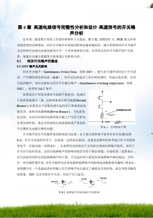
开关噪声给信号传输带来的影响更为显著,由于地引线和地平面存在寄生电感(见图6.1),在开关电流的作用下,会造成一定的电压波动,也就是说器件的参考地已经不再保持零电平。
在驱动端(见图6.2),本来要发送的低电平会因此出现相应的噪声波形,而对于开关信号波形来说,会因为地弹噪声的影响导致信号的下降沿变缓;在接收端(见图6.3),信号的波形同样会受到地弹噪声的干扰,不过这时的干扰波形和地弹噪声相位相反;另外,在一些存储性器件里,还有可能因为本身电源和地弹噪声的影响造成数据意外翻转(图6.4)。
如果耦合在一个选通或者时钟输入信号的噪声电压超过了阈值电压的时候,就会导致误触发的现象。
- 1、下载文档前请自行甄别文档内容的完整性,平台不提供额外的编辑、内容补充、找答案等附加服务。
- 2、"仅部分预览"的文档,不可在线预览部分如存在完整性等问题,可反馈申请退款(可完整预览的文档不适用该条件!)。
- 3、如文档侵犯您的权益,请联系客服反馈,我们会尽快为您处理(人工客服工作时间:9:00-18:30)。
Simultaneous Switching Noise in On-Chip CMOS Power Distribution NetworksKevin T.Tang and Eby G.Friedman,Fellow,IEEE Abstract—Simultaneous switching noise(SSN)has become animportant issue in the design of the internal on-chip power distri-bution networks in current very large scale integration/ultra largescale integration(VLSI/ULSI)circuits.An inductive model is usedto characterize the power supply rails when a transient current isgenerated by simultaneously switching the on-chip registers andlogic gates in a synchronous CMOS VLSI/ULSI circuit.An ana-lytical expression characterizing the SSN voltage is presented herebased on a lumped inductive-resistive-capacitiveFig.2.SSN within a ground rail.An analytical expression characterizing the on-chip SSN voltage is presented here based on alumpedth power law model [17],which is amore accurate device model than the Shichman–Hodges model for short-channel devices [18].The SSN voltage predicted by the analytical expression is compared to SPICE.The waveform describing the SSN voltage is quite close to the waveform obtained from SPICE simulation.The peak value of the SSN is within 10%of SPICE.Circuit-level design constraints,such as the number of simul-taneously switching logic gates connected to the same power supply rail,the drive current of the logic gates,the input transi-tion time,and the magnitude of the power supply are related to the peak value of the SSN.For a specific parasitic inductive-re-sistive-capacitiveth power law model,whichis more accurate than the alpha power law model in both the linear region and the saturation region [14].A CMOS logic gate in this discussion is modeled as a CMOS inverter.The power supply rail is characterized by alumped=2nH,R =0:1pF,=200ps.Fig.4.SSN voltage on a ground rail for 500simultaneously switching logic gates withL =5 ,C =29ps,andTANG AND FRIEDMAN:SSN IN ON-CHIP CMOS POWER DISTRIBUTION NETWORKS489Fig.5.The simultaneous switching voltage on a power rail withL =2nH,R =5 ,C =0:2pF, =200ps.Assuming that the magnitudeof.In order to derive an analytical expression for the differentialequation,are approximated by a polynomial expansion to the fifth order,where the average error is less than3%areindependent of the input transitiontimeare.The SSN voltage on a ground rail as predicted by (10)is compared to SPICE in Fig.3for a single CMOS inverterwithm,m,and mCMOS technology.The solid line represents the analytical pre-diction and the dashed line represents the results from SPICE simulations.During the time periodfrom490IEEE TRANSACTIONS ON VERY LARGE SCALE INTEGRATION (VLSI)SYSTEMS,VOL.10,NO.4,AUGUST 2002TABLE IP OLYNOMIAL E XPANSION C OEFFICIENTS OF A 0.5 m CMOS TECHNOLOGYThis analysis is based on a single inverter.If are pro-portionalto,the input slewrateis close to one(in a short-channel PMOS transistor is higher,typically inthe range of 1.5to 1.8(it is 1.68in the target0.5.The peak value of the SSN as compared to SPICE is shown inFig.6withm,m,and pF.The dashed line represents the peak value of the predicted SSN based on the analytical expression described by (15).The dotted line describes the results derived from the SPICE simulations.The accuracy of the analytical prediction is within 10%as compared to SPICE.The peak SSN voltage based on (15)is compared to SPICE for different conditions,as illustrated in Tables II and III for both the groundandps.Note that the maximum error of the analytical expression is within10%.Fig.6.The peak value of the SSN voltage withL =5 ,C =200ps.III.D ISCUSSIONThe dependence of the peak SSN voltage on the capacitive load is described insubsection,respectively.A.Capacitive LoadThe NMOS transistor is assumed here to operate in the satu-ration region before the input transition is completed.This as-sumption depends upon the input transition time,the capacitive load,and the device transconductance.Vemuru notes in [8]that the peak value of the SSN voltage depends on the capacitive load.The time when the NMOS transistor leaves the saturation re-gionis ,i.e.,Re-gion II,satisfies the constraint defined by (17).The horizontal dashed line represents the analytically predicted peak simulta-neous switching voltage.The accuracy of the analytical expres-sion in Region II is within 10%.Therefore,if the load capaci-tance and the input transition time satisfy the constraint defined by (17),the analytical prediction accurately estimates the peak SSN voltage.B.Circuit-Level ConstraintsThe SSN voltage should be less than atarget,can be determined basedonTANG AND FRIEDMAN:SSN IN ON-CHIP CMOS POWER DISTRIBUTION NETWORKS491TABLE IIC OMPARISON OF P EAK SSN V OLTAGE ON THE G ROUND R AILS,N UM IS THE N UMBER OF S IMULTANEOUSLY S WICHING L OGIC GATESTABLE III C OMPARISON OF P EAK SSN V OLTAGE ON THE V= 200ps.For example,the maximum number of simultaneously switching logic gates connected to the same power supply rail can be determined based on this constraint.Assumethatis the conditionof is the conditionofnH,pF,and m.492IEEE TRANSACTIONS ON VERY LARGE SCALE INTEGRATION (VLSI)SYSTEMS,VOL.10,NO.4,AUGUST2002Fig.8.The maximum number of simultaneously switching logic gates withL =5 ,andC is the voltage target,C 1: =3:6 m,C 2: =3:6 m,and C 3: =1:8m.Fig.9.Peak SSN as a function of the input transition time.Note the limiting constraints on the input transition time for different number of simultaneously switching gates,Num =1000;1500;and 2000.nH,pF are listed in Table IV ,note that for a very shortinput transition time,i.e.,20ps,the analytical model still pro-vides an accurate estimation of the peak noise.The analytical error is within 8%as listed in Table IV .Also note that the SSN voltage is proportional tothe).Therefore,the normalized si-multaneous switchingvoltage th)power of the supply voltage(,resistance),thickness(=2nH,R =0:1pF,and=2nH/cm,R =0:1pF/cm,Case 2:L =2 =cm,andC=1nH/cm,R=0:1pF/cm.Extraction of theparasitic,TANG AND FRIEDMAN:SSN IN ON-CHIP CMOS POWER DISTRIBUTION NETWORKS493 cm,and。