WM8978G资料
数据手册中文版

14位, 165M SPA(采样率)DAC(数模转换器)特性:●单电源供电+5V或+3V●高SFDR (无杂散动态范围): 在100MSPS 64dBc时20MHz输出●低干扰: 3PV -S●低功耗: 170MW (+5 V时)应用●通讯传输通道WLL , 蜂窝基站数字微波链路电缆调制解调器●波形产生直接数字频率合成器(DDS )任意波形发生器(ARB )●医疗/超声●高速仪表和控制●视频, 数字电视说明:DAC904是一款高速数模转换器, 14位分辨率, 引脚兼容DAC908、DAC900、DAC902, 分别提供8-, 10-, 12-位分辨率选择。
该系列DAC支持的所有型号更新率超过165MSPS, 具有优良的动态性能。
DAC904先进分割架构的优化为单音和多频音信号提供高无杂散动态范围(SFDR), 特别是用于通信系统的发送信号电路时。
DAC904具有高阻抗(200KΩ)的电流输出, 标称范围为20mA和一个最多为1.25V的输出。
差分输出允许两个差分或单端模拟信号的接口。
电流输出的匹配保证在差分结构中杰出的动态性能, 它可以与变压器配合使用。
运用一个小的几何CMOS工艺, 单片DAC904可以用在+2.7 V至+5.5 V宽的单电源范围内操作。
其低功耗特性允许它使用在便携式和电池供电系统情况下。
可通过减少输出电流与调整满量程选项实现进一步优化。
DAC904不断运转时, 掉电模式导致其待机功率仅为为45mW 。
DAC904带有一个集成的1.24V带隙基准和边沿触发输入锁存器, 提供完整的转换器解决方案。
+3 V和+5 V CMOS逻辑系列都可以接口到DAC904 。
DAC904的参考结构允许使用芯片上的参考, 或施加外部参考。
通过一个外部电阻, 满量程输出电流可以调整在2 - 20mA, 并保持其指定的动态性能。
DAC904采用SO -28和TSSOP -28封装。
绝对最大额定值+VA到AGND(模拟信号地)......-0.3V至+6V+VD到DGND(数字信号地)......-0.3V到+6VAGND到DGND......-0.3V到+0.3V+VA 到+VD......-6V到+6VCLK, PD到DGND......-0.3V到VD+0.3VD0-D13到DGND......-0.3V到VD+0.3VIOUT, I 到AGND......-1V到VA+0.3VBW,BYP到AGND......-0.3V到VA+0.3VREFIN ,FSA到AGND......-0.3V到VA+0.3VINT/EXT到AGND......-0.3V到VA+0.3V结温度. . . . . . . +150℃存储器温度. . . . . . +125℃防静电敏感度这种集成的电路可以被ESD(静电释放)损坏。
WM_W800_入门手册说明书
WM_W800_入门手册V1.2北京联盛德微电子有限责任公司(winner micro)地址:北京市海淀区阜成路67号银都大厦1802电话:+86-10-62161900公司网址:文档修改记录版本修订时间修订记录作者审核V0.12019/9/25[C]创建文档CuiycV0.22020/6/12增加cygwin编译环境CuiycV0.32020/7/8统一字体CuiycV1.02020/8/4添加硬件开发板CuiycV1.12020/11/5更新高速接口介绍RayCuiycV1.22021/2/4推荐使用IDE为CDK,不再维护CDS的工程目录文档修改记录 (2)目录 (3)1概述 (5)2准备工作 (5)3w800开发板简介 (6)4w800编译环境搭建 (7)4.1w800工具链 (7)4.2开发环境安装 (7)4.2.1Windows (7)4.2.2Linux (9)4.2.3Mac OS (10)5SDK工程获取 (10)6SDK工程编译 (10)6.1Windows (10)6.1.1Ubuntu虚拟机 (10)6.2Linux (11)6.3mac os (11)7固件烧录 (11)7.1Window下的操作步骤 (11)7.2Linux下升级步骤 (15)7.3Mac os下升级步骤 (15)8串口调试 (15)9w800 sdk如何开始编写用户程序 (15)9.1用户入口 (15)9.2demo如何使用 (16)9.3at指令如何使用 (16)1概述指导如何用户搭建w800硬件开发的软件环境,通过示例工程展示如何编译、下载固件到w800开发板等操作步骤。
该手册基于W800的ARDUINO开发板进行介绍及示例的升级运行。
w800是一款基于XT804内核SoC,支持功能:⚫ 2.4G Wi-Fi⚫蓝牙⚫内置多种数字接口(QFlash,外扩PSRAM,UART,GPIO,I²C,PWM,I²S,7816,SDIO,HSPI,TouchSensor)⚫支持多种硬件加解密算法(RC4,DES,3DES,AES,RSA,MD5,SHA1)⚫内置安全功能2准备工作硬件:⚫w800开发板⚫USB数据线(Micro USB)⚫PC(Windows、linux或Mac OS)软件:⚫工具链,用于编译w800代码⚫编译工具⚫w800 sdk⚫串口工具(支持xmodem协议)⚫代码编辑器3w800开发板简介W800 Arduino开发板,提供了如下接口:⚫I2C&I2S接口⚫Uart0&SWD调试接口⚫SPI&Uart1通信接口⚫PWM接口⚫SIM 接口⚫GPIO⚫Micro USB 接口用户通过Micro USB口与上位机相连,通过UART0口进行固件烧录。
M98 phone Manual说明书
手機待機界面 . . . . . . . . . . . . . 18
手機界面簡介 . . . . . . . . . . . . 19
手機捷徑使用説明 . . . . . . . . . . . 20
開啓捷徑功能 . . . . . . . . . . . . . 20 新增捷徑 . . . . . . . . . . . . . . 21
WEB 瀏覽器. . . . . . . . . . . . . 74
WEB 瀏覽器設定 . . . . . . . . . . . . 74 訪問網頁 . . . . . . . . . . . . . . 75 查看歷史記錄 . . . . . . . . . . . . . 75
4 影音庫應用程式
3 通訊應用程式
37
啓用電話功能 . . . . . . . . . . . . 37
撥打電話. . . . . . . . . . . . . . .37
接聽 / 拒聽電話 . . . . . . . . . . . . .41
快捷功能鍵 . . . . . . . . . . . . . .42
新增錄音記錄 . . . . . . . . . . . . . 91
播放方式 . . . . . . . . . . . . . . 92
播放錄音片段 . . . . . . . . . . . . . 92
複製 / 移動記錄 . . . . . . . . . . . . . 93
5 個人信息管理應用程式
歌曲管理 . . . . . . . . . . . . . . 86
設定背景音樂播放 . . . . . . . . . . . . 87
影片播放器 . . . . . . . . . . . . . 88
WM8978中文资料
描述 ........................................................................ 3 产品特征 .................................................................... 3
1
输入限幅器/电平自动控制(ALC)..................................... 25 ALC 芯片保护 .......................................................29 噪声门............................................................. 29 输出信号线路....................................................... 30 数字重放(DAC)线路................................................ 30 数字 Hi-Fi DAC 音量(增益)控制.....................................31 DAC 5 路均衡器 .....................................................32 DAC 3D 放大 ........................................................32 音量推动........................................................... 32 5 路图表均衡器 .....................................................34 3D 立体声放大 ......................................................36 模拟输出........................................................... 36 左和右通道混合器................................................... 36 耳机输出(LOUT1 和 ROUT1)..........................................39 扬声器输出(LOUT2 和 ROUT2)........................................41 零交叉间歇时间..................................................... 44 OUT3/OUT4 混合和输出 ...............................................44 输出使能........................................................... 48 过热保护........................................................... 48 未使用的模拟输入/输出.............................................. 48 数字音频接口....................................................... 51 主属和从属操作模式................................................. 51 音频数据模式....................................................... 51 音频接口控制....................................................... 54 环回............................................................... 54 压缩............................................................... 54 音频采样率......................................................... 55 主时钟和锁相环(PLL).............................................. 56 通用的输入/输出.................................................... 57 输出开关选择(插座检测)........................................... 58 控制接口........................................................... 59 控制模式选择和 2 线模式地址.........................................59 3 线串行控制模式 ...................................................59 2 线串行控制模式 ...................................................59 芯片复位........................................................... 60 电源............................................................... 60 推荐的上电/断电顺序................................................ 60 电源管理........................................................... 61 通过减少过采样率节省电能........................................... 61 VMID............................................................... 61 BIASEN............................................................. 61 源电流估算......................................................... 61
高通MSM8909核心板XY8901_硬件设计手册_V1.1
n8974a技术规格书
n8974a技术规格书1. 总览N8974A 是一款先进的高性能仪器,用于频谱分析和信号监测。
它采用了先进的数字信号处理技术,能够在宽频带范围内对复杂的信号进行分析,并提供高精度的测量数据。
该仪器适用于电信、无线通信、航空航天等领域,并具有广泛的应用价值。
2. 技术参数2.1 频率范围:100kHz-26.5GHz2.2 频率分辨率:1Hz2.3 动态范围:> 140dB2.4 相位噪声:-100dBc/Hz @ 10kHz offset2.5 输入阻抗:50Ω2.6 输入功率:最大+30dBm2.7 接口:USB、LAN3. 主要特点3.1 宽频带覆盖:N8974A 提供了从100kHz到26.5GHz的频率覆盖范围,能够对各种常用的无线信号进行全面的监测和分析。
3.2 高精度测量:采用了先进的数字信号处理技术,具有极高的动态范围和频率分辨率,能够提供高精度的测量数据。
3.3 自动化测试:支持远程控制和自动化测试,可以与测试系统集成,提高测试效率和准确性。
3.4 灵活的接口:具有标准的USB和LAN接口,可以方便地连接到计算机和网络,实现远程控制和数据传输。
3.5 友好的用户界面:采用了直观的操作界面和丰富的功能菜单,操作简便,易于上手。
4. 应用领域N8974A 在以下领域具有广泛的应用价值:4.1 电信领域:用于对移动通信、卫星通信等无线信号进行监测和分析,验证系统性能和信号质量。
4.2 无线通信领域:用于对WLAN、蓝牙、ZigBee等无线通信标准的信号进行测试和优化。
4.3 航空航天领域:用于航空雷达、导航系统等信号的监测和分析,确保系统的正常运行和安全性。
4.4 科研领域:用于科研机构和大学的实验室,支持各种频谱分析和无线信号研究。
5. 总结N8974A 是一款高性能的频谱分析仪,具有宽频带覆盖、高精度测量、自动化测试、灵活的接口和友好的用户界面等特点,适用于电信、无线通信、航空航天等领域,并具有广泛的应用价值。
WM8974_07资料

wWM8974Mono CODEC with Speaker DriverWOLFSON MICROELECTRONICS plc Production Data, Rev 4.2 March 2007DESCRIPTIONThe WM8974 is a low power, high quality mono CODEC designed for portable applications such as Digital Still Camera or Digital Voice Recorder.The device integrates support for a differential or single ended mic, and includes drivers for speakers or headphone, and mono line output. External component requirements are reduced as no separate microphone or headphone amplifiers are required.Advanced Sigma Delta Converters are used along with digital decimation and interpolation filters to give high quality audio at sample rates from 8 to 48ks/s. Additional digital filtering options are available in the ADC path, to cater for application filtering such as ‘wind noise reduction’, plus an advanced mixed signal ALC function with noise gate is provided. The digital audio interface supports A-law and µ-law companding. An on-chip PLL is provided to generate the required Master Clock from an external reference clock. The PLL clock can also be output if required elsewhere in the system.The WM8974 operates at supply voltages from 2.5 to 3.6V, although the digital supplies can operate at voltages down to 1.71V to save power. The speaker and mono outputs use a separate supply of up to 5V which enables increased output power if required. Different sections of the chip can also be powered down under software control by way of the selectable two or three wire control interface.WM8974 is supplied in a very small 4x4mm QFN package, offering high levels of functionality in minimum board area, with high thermal performance.FEATURES• Mono CODEC:• Audio sample rates:8, 11.025, 16, 22.05, 24, 32, 44.1, 48kHz • DAC SNR 98dB, THD -84dB (‘A’-weighted @ 8 – 48ks/s) • ADC SNR 94dB, THD -83dB (‘A’-weighted @ 8 – 48ks/s) • On-chip Headphone/Speaker Driver with ‘cap-less’ connect - 40mW output power into 16Ω / 3.3V SPKVDD - BTL speaker drive 0.9W into 8Ω / 5V SPKVDD • Additional MONO Line output• Multiple analog or ‘Aux’ inputs, plus analog bypass path • Mic Preamps:•Differential or single end Microphone Interface - Programmable preamp gain- Psuedo differential inputs with common mode rejection - Programmable ALC / Noise Gate in ADC path •Low-noise bias supplied for electret microphonesOTHER FEATURES• 5 band EQ (record or playback path) • Digital Playback Limiter• Programmable ADC High Pass Filter (wind noise reduction) • Programmable ADC Notch Filter • On-chip PLL• Low power, low voltage- 2.5V to 3.6V (digital: 1.71V to 3.6V)- power consumption <10mA all-on 48ks/s mode • 4x4x0.9mm 24 lead QFN packageAPPLICATIONS• Digital Still Camera Audio Codec• Wireless VoIP and other communication device handsets / headsets• Portable audio recorder•General Purpose low power audio CODECWM8974Production DataTABLE OF CONTENTS DESCRIPTION (1)FEATURES (1)APPLICATIONS (1)TABLE OF CONTENTS (2)PIN CONFIGURATION (3)ORDERING INFORMATION (3)PIN DESCRIPTION (4)ABSOLUTE MAXIMUM RATINGS (5)RECOMMENDED OPERATING CONDITIONS (5)ELECTRICAL CHARACTERISTICS (6)TERMINOLOGY (8)SIGNAL TIMING REQUIREMENTS (9)SYSTEM CLOCK TIMING (9)AUDIO INTERFACE TIMING – MASTER MODE (9)AUDIO INTERFACE TIMING – SLAVE MODE (10)CONTROL INTERFACE TIMING – 3-WIRE MODE (11)CONTROL INTERFACE TIMING – 2-WIRE MODE (12)DEVICE DESCRIPTION (13)INTRODUCTION (13)INPUT SIGNAL PATH (14)ANALOGUE TO DIGITAL CONVERTER (ADC) (19)INPUT LIMITER / AUTOMATIC LEVEL CONTROL (ALC) (23)OUTPUT SIGNAL PATH (35)ANALOGUE OUTPUTS (42)OUTPUT SWITCH (47)DIGITAL AUDIO INTERFACES (49)AUDIO SAMPLE RATES (54)MASTER CLOCK AND PHASE LOCKED LOOP (PLL) (55)GENERAL PURPOSE INPUT/OUTPUT (57)CONTROL INTERFACE (57)RESETTING THE CHIP (58)POWER SUPPLIES (58)POWER MANAGEMENT (63)REGISTER MAP (65)REGISTER BITS BY ADDRESS (66)DIGITAL FILTER CHARACTERISTICS (77)TERMINOLOGY (77)DAC FILTER RESPONSES (78)ADC FILTER RESPONSES (78)DE-EMPHASIS FILTER RESPONSES (79)HIGHPASS FILTER (80)5-BAND EQUALISER (81)APPLICATIONS INFORMATION (85)RECOMMENDED EXTERNAL COMPONENTS (85)PACKAGE DIAGRAM (86)IMPORTANT NOTICE (87)ADDRESS: (87)Production Data WM8974 PIN CONFIGURATIONTOPVIEWORDERING INFORMATIONORDER CODE TEMPERATURERANGE PACKAGE MOISTURESENSITIVITYLEVELPACKAGE BODYTEMPERATUREWM8974GEFL/V -25°C to +85°C 24-lead QFN (4x4x0.9mm)(Pb-free)MSL3 260o CWM8974GEFL/RV -25°C to +85°C 24-lead QFN (4x4x0.9mm)(Pb-free, tape and reel)MSL3 260o C Note:Reel Quantity = 3,500WM8974Production Data PIN DESCRIPTIONPIN NO NAME TYPE DESCRIPTION1 MICBIAS Analogue Output Microphone bias2 AVDD Supply Analogue supply (feeds ADC and DAC)3 AGND Supply Analogue ground (feeds ADC and DAC)4 DCVDD Supply Digital core supply5 DBVDD Supply Digital buffer (input/output) supplyground6 DGND Supply Digital7 ADCDAT Digital Output ADC digital audio data output8 DACDAT Digital Input DAC digital audio data input9 FRAME Digital Input / Output DAC and ADC sample rate clock or frame synch10 BCLK Digital Input / Output Digital audio port clock11 MCLK Digital Input Master clock input12 CSB/GPIO Digital Input / Output 3-Wire MPU chip select or general purpose input/output pin.13 SCLK Digital Input 3-Wire MPU clock Input / 2-Wire MPU Clock Input14 SDIN Digital Input / Output 3-Wire MPU data Input / 2-Wire MPU Data Input15 MODE Digital Input Control interface mode selection pin.Analogue Output Mono output16 MONOOUTAnalogue Output Speaker output positive17 SPKOUTPSupply Speaker ground (feeds speaker and mono output amps only)18 SPKGNDAnalogue Output Speaker output Negative19 SPKOUTNSupply Speaker supply (feeds speaker and mono output amps only)20 SPKVDDAnalogue Input Auxiliary analogue input21 AUXReference Decoupling for midrail reference voltage22 VMIDAnalogue Input Microphone negative input23 MICNAnalogue Input Microphone positive input (common mode)24 MICPNote:It is recommended that the QFN ground paddle should be connected to analogue ground on the application PCB.Production DataWM8974ABSOLUTE MAXIMUM RATINGSAbsolute Maximum Ratings are stress ratings only. Permanent damage to the device may be caused by continuouslyoperating at or beyond these limits. Device functional operating limits and guaranteed performance specifications are given under Electrical Characteristics at the test conditions specified.ESD Sensitive Device. This device is manufactured on a CMOS process. It is therefore generically susceptible to damage from excessive static voltages. Proper ESD precautions must be taken during handling and storage of this device.Wolfson tests its package types according to IPC/JEDEC J-STD-020B for Moisture Sensitivity to determine acceptable storage conditions prior to surface mount assembly. These levels are:MSL1 = unlimited floor life at <30°C / 85% Relative Humidity. Not normally stored in moisture barrier bag. MSL2 = out of bag storage for 1 year at <30°C / 60% Relative Humidity. Supplied in moisture barrier bag. MSL3 = out of bag storage for 168 hours at <30°C / 60% Relative Humidity. Supplied in moisture barrier bag. The Moisture Sensitivity Level for each package type is specified in Ordering Information. CONDITION MIN MAXDBVDD, DCVDD, AVDD supply voltages -0.3V +4.2 SPKVDD supply voltage -0.3V +7V Voltage range digital inputs DGND -0.3V DVDD +0.3V Voltage range analogue inputs AGND -0.3VAVDD +0.3VOperating temperature range, T A -25°C +85°CStorage temperature prior to soldering 30°C max / 85% RH max Storage temperature after soldering -65°C +150°CNotes 1. Analogue and digital grounds must always be within 0.3V of each other. 2. All digital and analogue supplies are completely independent from each other.RECOMMENDED OPERATING CONDITIONSPARAMETER SYMBOL TEST CONDITIONS MIN TYP MAX UNITDigital supply range (Core) DCVDD 1.71 3.6 VDigital supply range (Buffer) DBVDD 1.71 3.6 V Analogue supplies range AVDD 2.5 3.6 VSpeaker supply SPKVDD 2.5 5.5 VGround DGND,AGND,SPKGNDVNotes 1. When using PLL, DCVDD must be 1.9V or higher. 2. AVDD must be ≥ DCVDD.3. DBVDD must be ≥ DCVDD.4. In non-boosted mode, SPKVDD must be ≥ AVDD, if boosted SPKVDD must be ≥ 1.5x AVDD.5.When using PLL, DCVDD must be ≥ 1.9V.WM8974Production DataELECTRICAL CHARACTERISTICSTest ConditionsDCVDD = 1.8V, AVDD = DBVDD = 3.3V, SPKVDD = 3.3V, T A = +25o C, 1kHz signal, fs = 48kHz, 24-bit audio data unless otherwise stated.PARAMETER SYMBOL TEST CONDITIONS MIN TYP MAX UNIT Microphone Inputs (MICN, MICP) Full-scale Input Signal Level (Note 1) – note this changes with AVDDV INFSPGABOOST = 0dB INPPGAVOL = 0dB1.0 0 VrmsdBVMic PGA equivalent input noise At 35.25dBgain 150 uVInput resistance R MICIN Gain set to 35.25dB 1.6 k Ω Input resistance R MICIN Gain set to 0dB 47 k Ω Input resistance R MICIN Gain set to -12dB 75 k Ω Input resistance R MICIP MICP2INPPGA = 1 94 k Ω Input resistance R MICIP MICP2INPPGA = 094k ΩInput Capacitance C MICIN 10 pF MIC Input Programmable Gain Amplifier (PGA)Programmable Gain-12 35.25 dBProgrammable Gain Step Size Guaranteed monotonic0.75dBMute Attenuation 108 dB Selectable Input Gain Boost (0/+20dB)Gain Boost 0 20 dB Automatic Level Control (ALC)/Limiter – ADC onlyTarget Record Level -28.5 -6 dB Programmable Gain-12 35.25 dBProgrammable Gain Step Size Guaranteed Monotonic0.75dB Gain Hold Time (Note 2)t HOLD MCLK=12.288MHz (Note 4) 0, 2.67, 5.33, 10.67, … , 43691 (time doubles with each step) ms ALCMODE=0 (ALC), MCLK=12.288MHz(Note 4) 3.3, 6.6, 13.1, … , 3360 (time doubles with each step) Gain Ramp-Up (Decay) Time (Note 3)t DCYALCMODE=1 (limiter), MCLK=12.288MHz(Note 4)0.73, 1.45, 2.91, … , 744 (time doubles with each step) msALCMODE=0 (ALC), MCLK=12.288MHz(Note 4) 0.83, 1.66, 3.33, … , 852 (time doubles with each step) Gain Ramp-Down (Attack) Time (Note 3)t ATKALCMODE=1 (limiter), MCLK=12.288MHz(Note 4)0.18, 0.36, 0.73, … , 186 (time doubles with each step)msAnalogue to Digital Converter (ADC) Signal to Noise Ratio (Note 5) SNR A-weighted,0dB PGA gain 85 94 dB Total Harmonic Distortion (Note 6)THD-1dBFS input, 0dB PGA gain-75 -83 dBAuxilliary Analogue Input (AUX) Full-scale Input Signal Level (0dB) – note this changes with AVDD V INFS 1.0 0 VrmsdBVInput Resistance R AUXIN AUXMODE =0 20 k ΩInput Capacitance C AUXIN10 pFProduction DataWM8974Test ConditionsDCVDD = 1.8V, AVDD = DBVDD = 3.3V, SPKVDD = 3.3V, T A = +25o C, 1kHz signal, fs = 48kHz, 24-bit audio data unless otherwise stated.PARAMETER SYMBOL TEST CONDITIONS MIN TYP MAX UNIT Digital to Analogue Converter (DAC) to MONO output (all data measured with 10k Ω / 50pF load) Signal to Noise Ratio (Note 5) SNR A-weighted 90 98 dB Total Harmonic Distortion + Noise (Note 6)THD+N R L = 10 k Ωfull-scale signal-84 dBMONOBOOST =0 AVDD/3.30dB Full Scale output voltage (Note 9)MONOBOOST=11.5x(AVDD/3.3)V RMS Speaker Output PGA Programmable Gain-57 6 dBProgrammable Gain Step SizeGuaranteed monotonic1dBBTL Speaker Output (SPKOUTP, SPKOUTN with 8Ω bridge tied load)Output PowerP O Output power is very closely correlated with THD; see belowP O =180mW, R L = 8Ω,SPKVDD=3.3V 0.03 -70 % dB P O =400mW, R L = 8Ω,SPKVDD=3.3V 5.0 -26 % dB P O =360mW, R L = 8Ω,SPKVDD=5V 0.02 -75 % dB Total Harmonic Distortion + Noise (Note 6)THD+NP O =800mW, R L = 8Ω,SPKVDD=5V0.06 -65 % dB SPKVDD=3.3V,R L = 8Ω 90 101 dB Signal to Noise RatioSNRSPKVDD=5V, R L = 8Ω102 dBPower Supply Rejection Ratio50 dB‘Headphone’ output (SPKOUTP, SPKOUTN with resistive load to ground)Signal to Noise RatioSNR 100 dB Total Harmonic Distortion + Noise (Note 6) THD+N Po =20mW, R L = 16Ω,SPKVDD=3.3V0.02 -74 %dBPo=20mW, R L = 32Ω, SPKVDD=3.3V0.017 - 75 % dB Microphone Bias Bias Voltage (MBVSEL=0) V MICBIAS0.9*AVDDVBias Voltage (MBVSEL=1) V MICBIAS 0.65*AVDD V Bias Current Source I MICBIAS 3 mA Output Noise Voltage Vn1K to 20kHz15nV/√HzDigital Input / Output Input HIGH Level V IH 0.7×DVDD V Input LOW Level V IL 0.3×DVDD VOutput HIGH Level V OH I OL =1mA 0.9×DVDDVOutput LOW LevelV OLI OH -1mA 0.1xDVDD VWM8974Production Data TERMINOLOGY1. MICN input only in single ended microphone configuration. Maximum input signal to MICP without distortion is -3dBV.2. Hold Time is the length of time between a signal detected being too quiet and beginning to ramp up the gain. It doesnot apply to ramping down the gain when the signal is too loud, which happens without a delay.3. Ramp-up and Ramp-Down times are defined as the time it takes for the PGA to change it’s gain by 6dB.4. All hold, ramp-up and ramp-down times scale proportionally with MCLK5. Signal-to-noise ratio (dB) – SNR is a measure of the difference in level between the full scale output and the output withno signal applied. (No Auto-zero or Automute function is employed in achieving these results).6. THD+N (dB) – THD+N is a ratio, of the rms values, of (Noise + Distortion)/Signal.7. The maximum output voltage can be limited by the speaker power supply. If MONOBOOST=1 then SPKVDD shouldbe 1.5xAVDD or higher to prevent clipping taking place in the output stage.Production DataWM8974SIGNAL TIMING REQUIREMENTSSYSTEM CLOCK TIMINGFigure 1 System Clock Timing RequirementsTest ConditionsDCVDD=1.8V, DBVDD=AVDD=SPKVDD=3.3V, DGND=AGND=SPKGND=0V, T A = +25o CPARAMETER SYMBOL CONDITIONS MIN TYP MAX UNIT System Clock Timing Information MCLK=SYSCLK (=256fs)81.38ns MCLK cycle time T MCLKYMCLK input to PLL Note 1 20nsMCLK duty cycle T MCLKDS 60:40 40:60Note 1:PLL pre-scaling and PLL N and K values should be set appropriately so that SYSCLK is no greater than 12.288MHz.AUDIO INTERFACE TIMING – MASTER MODEFigure 2 Digital Audio Data Timing – Master Mode (see Control Interface)WM8974Production DataTest ConditionsDCVDD=1.8V, DBVDD=AVDD=SPKVDD=3.3V, DGND=AGND=SPKGND=0V, T A =+25o C, Master Mode, fs=48kHz, MCLK=256fs,24-bit data, unless otherwise stated. PARAMETER SYMBOL MIN TYP MAX UNITAudio Data Input Timing InformationFRAME propagation delay from BCLK falling edge t DL 10 ns ADCDAT propagation delay from BCLK falling edge t DDA 10 ns DACDAT setup time to BCLK rising edge t DST 10 ns DACDAT hold time from BCLK rising edge t DHT 10 nsNote:BCLK period should always be greater than MCLK period.AUDIO INTERFACE TIMING – SLAVE MODEFigure 3 Digital Audio Data Timing – Slave ModeTest ConditionsDCVDD=1.8V, DBVDD=AVDD=SPKVDD=3.3V, DGND=AGND=SPKGND=0V, T A =+25o C, Slave Mode, fs=48kHz, MCLK= 256fs, 24-bit data, unless otherwise stated.PARAMETER SYMBOL MIN TYP MAX UNIT Audio Data Input Timing InformationBCLK cycle time t BCY 160 ns BCLK pulse width high t BCH 64 ns BCLK pulse width lowt BCL 64 ns FRAME set-up time to BCLK rising edge t LRSU 10 ns FRAME hold time from BCLK rising edge t LRH 10 ns DACDAT hold time from BCLK rising edge t DH 10 ns DACDAT set-up time to BCLK rising edge t DS 10 ns ADCDAT propagation delay from BCLK falling edge t DD 20 nsCONTROL INTERFACE TIMING – 3-WIRE MODEFigure 4 Control Interface Timing – 3-Wire Serial Control ModeTest ConditionsDCVDD = 1.8V, DBVDD = AVDD = SPKVDD = 3.3V, DGND = AGND = SPKGND = 0V, T A = +25o C, Slave Mode, fs = 48kHz,MCLK = 256fs, 24-bit data, unless otherwise stated.UNITMAXTYPMINPARAMETER SYMBOLProgram Register Input InformationSCLK rising edge to CSB rising edge t SCS 80 nsSCLK pulse cycle time t SCY 200 nsSCLK pulse width low t SCL 80 nsSCLK pulse width high t SCH 80 nsSDIN to SCLK set-up time t DSU 40 nsSCLK to SDIN hold time t DHO 40 nsCSB pulse width low t CSL 40 nsCSB pulse width high t CSH 40 nsCSB rising to SCLK rising t CSS 40 nsPulse width of spikes that will be suppressed t ps 0 5nsCONTROL INTERFACE TIMING – 2-WIRE MODEFigure 5 Control Interface Timing – 2-Wire Serial Control ModeTest ConditionsDCVDD=1.8V, DBVDD=AVDD=SPKVDD=3.3V, DGND=AGND=SPKGND=0V, T A = +25o C, Slave Mode, fs = 48kHz, MCLK =256fs, 24-bit data, unless otherwise stated.UNITMAX PARAMETER SYMBOLTYPMINProgram Register Input InformationSCLK Frequency 0 526kHzSCLK Low Pulse-Width t1 1.3 usSCLK High Pulse-Width t2 600 nsHold Time (Start Condition) t3 600 nsSetup Time (Start Condition) t4 600 nsData Setup Time t5 100 nsSDIN, SCLK Rise Time t6300nsSDIN, SCLK Fall Time t7300nsSetup Time (Stop Condition) t8 600 nsData Hold Time t9900nsnsPulse width of spikes that will be suppressed t ps 0 5DEVICE DESCRIPTIONINTRODUCTIONThe WM8974 is a low power audio codec combining a high quality mono audio DAC and ADC, withflexible line and microphone input and output processing. Applications for this device include digitalstill cameras with mono audio, record and playback capability, voice recorders, wireless VoIPheadsets and games console accessories.FEATURESThe chip offers great flexibility in use, and so can support many different modes of operation asfollows:MICROPHONE INPUTSTwo microphone inputs are provided, allowing for either a differential microphone input or a singleended microphone to be connected. These inputs have a user programmable gain range of -12dBto +35.25dB using internal resistors. After the input PGA stage comes a boost stage which can adda further 20dB of gain. A microphone bias is output from the chip which can be used to bias themicrophones. The signal routing can be configured to allow manual adjustment of mic levels, or toallow the ALC loop to control the level of mic signal that is transmitted.Total gain through the microphone paths of up to +55.25dB can be selected.PGA AND ALC OPERATIONA programmable gain amplifier is provided in the input path to the ADC. This may be used manuallyor in conjunction with a mixed analogue/digital automatic level control (ALC) which keeps therecording volume constant.AUX INPUTThe device includes a mono input, AUX, that can be used as an input for warning tones (beep) etc.The output from this circuit can be summed into the mono output and/or the speaker output paths,so allowing for mixing of audio with ‘backing music’ etc as required. This path can also be summedinto the input in a flexible fashion, either to the input PGA as a second microphone input or as a lineinput. The configuration of this circuit, with integrated on-chip resistors allows several analoguesignals to be summed into the single AUX input if required.ADCThe mono ADC uses a multi-bit high-order oversampling architecture to deliver optimumperformance with low power consumption. Various sample rates are supported, from the 8ks/s ratetypically used in voice dictation, up to the 48ks/s rate used in high quality audio applications.HI-FI DACThe hi-fi DAC provides high quality audio playback suitable for all portable mono audio typeapplications.DIGITAL FILTERINGAdvanced Sigma Delta Converters are used along with digital decimation and interpolation filters togive high quality audio at sample rates from 8ks/s to 48ks/s.Application specific digital filters are also available which help to reduce the effect of specific noisesources such as ‘wind noise’. The filters include a programmable ADC high pass filter, aprogrammable ADC notch filter and a 5-band equaliser that can be applied to either the ADC or theDAC path in order to improve the overall audio sound from the device.OUTPUT MIXING AND VOLUME ADJUSTFlexible mixing is provided on the outputs of the device; a mixer is provided for the speaker outputs,and an additional mono summer for the mono output. These mixers allow the output of the DAC, theoutput of the ADC volume control and the Auxilliary input to be combined. The output volume canbe adjusted using the integrated digital volume control and there is additional analogue gainadjustment capability on the speaker output.AUDIO INTERFACESThe WM8974 has a standard audio interface, to support the transmission of audio data to and fromthe chip. This interface is a 4 wire standard audio interface which supports a number of audio dataformats including I2S, DSP Mode, MSB-First, left justified and MSB-First, right justified, and canoperate in master or slave modes.CONTROL INTERFACESTo allow full software control over all its features, the WM8974 offers a choice of 2 or 3 wire MPUcontrol interface. It is fully compatible and an ideal partner for a wide range of industry standardmicroprocessors, controllers and DSPs. The selection between 2-wire mode and 3-wire mode isdetermined by the state of the MODE pin. If MODE is high then 3-wire control mode is selected, ifMODE is low then 2-wire control mode is selected.In 2 wire mode, only slave operation is supported, and the address of the device is fixed as 0011010.CLOCKING SCHEMESWM8974 offers the normal audio DAC clocking scheme operation, where 256fs MCLK is provided tothe DAC/ADC.However, a PLL is also included which may be used to generate the internal master clock frequencyin the event that this is not available from the system controller. This PLL uses an input clock,typically the 12MHz USB or ilink clock, to generate high quality audio clocks. If this PLL is notrequired for generation of these clocks, it can be reconfigured to generate alternative clocks whichmay then be output on the CSB/GPIO pin and used elsewhere in the system.POWER CONTROLThe design of the WM8974 has given much attention to power consumption without compromisingperformance. It operates at low supply voltages, and includes the facility to power off any unusedparts of the circuitry under software control, includes standby and power off modes.INPUT SIGNAL PATHThe WM8974 has 3 flexible analogue inputs: two microphone inputs, and an auxiliary input. Theseinputs can be used in a variety of ways. The input signal path before the ADC has a flexible PGAblock which then feeds into a gain boost/mixer stage.MICROPHONE INPUTSThe WM8974 can accommodate a variety of microphone configurations including single ended anddifferential inputs. The inputs through the MICN, MICP and optionally AUX pins are amplifiedthrough the input PGA as shown in Figure 6 .A pseudo differential input is the preferential configuration where the positive terminal of the inputPGA is connected to the MICP input pin by setting MICP2INPPGA=1. The microphone groundshould then be connected to MICN (when MICN2INPPGA=1) or optionally to AUX (whenAUX2INPPGA=1) input pins.Alternatively a single ended microphone can be connected to the MICN input with MICN2INPPGA setto 1. The non-inverting terminal of the input PGA should be connected internally to VMID by settingMICP2INPPGA to 0.In differential mode the larger signal should be input to MICP and the smaller (e.g. noisy groundconnection) should be input to MICN.Figure 6 Microphone Input PGA Circuit (switch positions shown are for differential mic input)REGISTER ADDRESS BIT LABEL DEFAULT DESCRIPTIONMICP2INPPGA1Connect input PGA amplifier positive terminal to MICP or VMID.0 = input PGA amplifier positive terminal connected to VMID1 = input PGA amplifier positive terminal connected to MICP through variable resistor string1 MICN2INPPGA 1Connect MICN to input PGA negative terminal. 0=MICN not connected to input PGA1=MICN connected to input PGA amplifier negative terminal.R44Input Control2 AUX2INPPGA 0Select AUX amplifier output as input PGA signal source.0=AUX not connected to input PGA1=AUX connected to input PGA amplifier negative terminal.The input PGA is enabled by the IPPGAEN register bit.REGISTER ADDRESS BIT LABEL DEFAULTDESCRIPTIONR2 PowerManagement 2 2INPPGAENInput microphone PGA enable0 = disabled 1 = enabledINPUT PGA VOLUME CONTROLThe input microphone PGA has a gain range from -12dB to +35.25dB in 0.75dB steps. The gain from the MICN input to the PGA output and from the AUX amplifier to the PGA output are always common and controlled by the register bits INPPGAVOL[5:0]. These register bits also affect the MICP pin when MICP2INPPGA=1.When the Automatic Level Control (ALC) is enabled the input PGA gain is then controlled automatically and the INPPGAVOL bits should not be used. REGISTER ADDRESSBIT LABEL DEFAULTDESCRIPTION5:0 INPPGAVOL010000Input PGA volume 000000 = -12dB 000001 = -11.25db .010000 = 0dB .111111 = 35.25dB6 INPPGAMUTE 0Mute control for input PGA:0=Input PGA not muted, normal operation1=Input PGA muted (and disconnected from the following input BOOST stage).R45 Input PGA volume control7 INPPGAZC 0Input PGA zero cross enable:0=Update gain when gain register changes 1=Update gain on 1st zero cross after gain register write.R32ALC control 18 ALCSEL 0ALC function select:0=ALC off (PGA gain set by INPPGAVOL register bits)1=ALC on (ALC controls PGA gain)Table 1 Input PGA Volume ControlAUXILLIARY INPUTAn auxilliary input circuit (Figure 7) is provided which consists of an amplifier which can be configured either as an inverting buffer for a single input signal or as a mixer/summer for multiple inputs with the use of external resistors. The circuit is enabled by the register bit AUXEN.Figure 7 Auxiliary Input CircuitThe AUXMODE register bit controls the auxiliary input mode of operation:In buffer mode (AUXMODE=0) the switch labelled AUXSW in Figure 7 is open and the signal at the AUX pin will be buffered and inverted through the aux circuit using only the internal components.In mixer mode (AUXMODE=1) the on-chip input resistor is bypassed, this allows the user to sum in multiple inputs with the use of external resistors. When used in this mode there will be gain variations through this path from part to part due to the variation of the internal 20k Ω resistors relative to the higher tolerance external resistors.REGISTER ADDRESS BIT LABEL DEFAULT DESCRIPTIONR1 Powermanagement 1 6AUXENAuxiliary input buffer enable 0 = OFF 1 = ONR44Input control3 AUXMODE 00 = inverting buffer1 = mixer (on-chip input resistor bypassed)Table 2 Auxiliary Input Buffer ControlINPUT BOOSTThe input BOOST circuit has 3 selectable inputs: the input microphone PGA output, the AUX amplifier output and the MICP input pin (when not using a differential microphone configuration). These three inputs can be mixed together and have individual gain boost/adjust as shown in Figure8.Figure 8 Input Boost StageThe input PGA path can have a +20dB boost (PGABOOST=1) a 0dB pass through (PGABOOST=0) or be completely isolated from the input boost circuit (INPPGAMUTE=1).REGISTER ADDRESS BIT LABEL DEFAULT DESCRIPTIONR45Input PGA gain control6INPPGAMUTEMute control for input PGA:0=Input PGA not muted, normal operation1=Input PGA muted (and disconnected from the following input BOOST stage).R47Input BOOST control8 PGABOOST 00 = PGA output has +0dB gain through input BOOST stage.1 = PGA output has +20dB gain through input BOOST stage.Table 3 Input BOOST Stage ControlThe Auxiliary amplifier path to the BOOST stage is controlled by the AUX2BOOSTVOL[2:0] register bits. When AUX2BOOSTVOL=000 this path is completely disconnected from the BOOST stage. Settings 001 through to 111 control the gain in 3dB steps from -12dB to +6dB.。
WM产品规格书
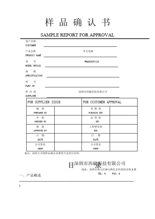
样 品 确 认 书SAMPLE REPORT FOR APPROVAL客户名称CUSTOMER 产品名称开关电源PRODUCT NAME 型 号WMAH250T120MODEL DETAIL 规 格SPECIFICATION 料 号PART NO 供 应 商深圳市西磁科技有限公司备注:请贵公司将样品确认结果签字盖章后回传。
目 录一、产品概述----------------------------------------------------------------------------------------2深圳市西磁科技有限公司地址:深圳市南山区丽山路民企科技园3栋5搂TEL :6 FAX :6二、产品主要---------------------------------------------------------------------------------------- 2三、引用标准及规范----------------------------------------------------------------------------- 2四、环境条件---------------------------------------------------------------------------------------- 2五、电气特性---------------------------------------------------------------------------------------- 3六、保护特性--------------------------------------------------------------------------------------- 3七、安规要求---------------------------------------------------------------------------------------47-1 绝缘强度和绝缘阻抗------------------------------------------------------------------- 47-2 漏电流------------------------------------------------------------------------------------- 4八、产品安装、使用说明8-2 运输----------------------------------------------------------------------------------- 48-3 储存----------------------------------------------------------------------------------- 4九、包装、运输、储存十、外观尺寸10-1外形尺寸------------------------------------------------------------------------------ 510-3定位尺寸及外观图------------------------------------------------------------------- 510-3 端子定义----------------------------------------------------------------------------- 5一、产品概述1-1.低成本和高可靠性。
- 1、下载文档前请自行甄别文档内容的完整性,平台不提供额外的编辑、内容补充、找答案等附加服务。
- 2、"仅部分预览"的文档,不可在线预览部分如存在完整性等问题,可反馈申请退款(可完整预览的文档不适用该条件!)。
- 3、如文档侵犯您的权益,请联系客服反馈,我们会尽快为您处理(人工客服工作时间:9:00-18:30)。
• Stereo Codec: • DAC SNR 98dB, THD -84dB (‘A’ weighted @ 48kHz) • ADC SNR 90dB, THD -80dB (‘A’ weighted @ 48kHz) • On-chip Headphone Driver with ‘capless’ option
TERMINOLOGY ............................................................................................................ 9 POWER CONSUMPTION ....................................................................................10 SIGNAL TIMING REQUIREMENTS .....................................................................11
Advanced on-chip digital signal processing includes a 5-band equaliser, a mixed signal Automatic Level Control for the microphone or line input through the ADC as well as a purely digital limiter function for record or playback. Additional digital filtering options are available in the ADC path, to cater for application filtering such as ‘wind noise reduction’.
SYSTEM CLOCK TIMING ........................................................................................... 11 AUDIO INTERFACE TIMING – MASTER MODE ........................................................ 11 AUDIO INTERFACE TIMING – SLAVE MODE............................................................ 12 CONTROL INTERFACE TIMING – 3-WIRE MODE .................................................... 13 CONTROL INTERFACE TIMING – 2-WIRE MODE .................................................... 14 DEVICE DESCRIPTION.......................................................................................15 INTRODUCTION ......................................................................................................... 15 INPUT SIGNAL PATH ................................................................................................. 17 ANALOGUE TO DIGITAL CONVERTER (ADC).......................................................... 23 INPUT LIMITER / AUTOMATIC LEVEL CONTROL (ALC) .......................................... 27 OUTPUT SIGNAL PATH ............................................................................................. 31 3D STEREO ENHANCEMENT .................................................................................... 37 ANALOGUE OUTPUTS............................................................................................... 38 DIGITAL AUDIO INTERFACES................................................................................... 52 AUDIO SAMPLE RATES ............................................................................................. 59 MASTER CLOCK AND PHASE LOCKED LOOP (PLL) ............................................... 59 GENERAL PURPOSE INPUT/OUTPUT...................................................................... 61 OUTPUT SWITCHING (JACK DETECT)..................................................................... 62 CONTROL INTERFACE.............................................................................................. 63 RESETTING THE CHIP .............................................................................................. 64 POWER SUPPLIES .................................................................................................... 64 POWER MANAGEMENT ............................................................................................ 65 REGISTER MAP...................................................................................................67 DIGITAL FILTER CHARACTERISTICS ...............................................................69 TERMINOLOGY .......................................................................................................... 69 DAC FILTER RESPONSES......................................................................................... 70 ADC FILTER RESPONSES......................................................................................... 70 HIGHPASS FILTER..................................................................................................... 71 5-BAND EQUALISER .................................................................................................. 72 APPLICATIONS INFORMATION .........................................................................76 RECOMMENDED EXTERNAL COMPONENTS .......................................................... 76 PACKAGE DIAGRAM ..........................................................................................77 IMPORTANT NOTICE ..........................................................................................78 ADDRESS: .................................................................................................................. 78