UPSD3233B-40T1中文资料
UPS 操作手册完整版
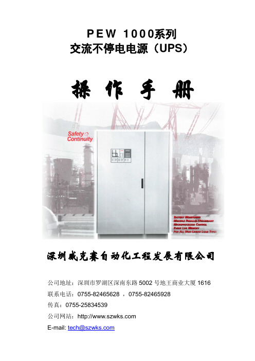
接点
组件
解释
F021
逆变器输出保险
当逆变器发生重大故障时保护负载,当逆变器发生重大故障时系统将会切换到旁路,同时保险F021将会断开并不影响输出电压。前面板将会显示警报
A035
(A030)
静态旁路转换开关EN
具有3组不平行转换电源可控硅
A201
内部电源供应
由内部整流器主线或旁路主线供电,此供电是内部供电冗余系统的一部分与A202一起由电池供电,二者之中的每一个都可以充足为系统供电,当二者之中的一个发生故障,前面板将会将会发出警报
每一个并机系统是独立的,有其独立的旁路,除了输出配电柜,不再需要其他的共用组件或者中央部件
一个有问题的系统将会立刻与输出配电柜隔离
负载为各个独立的系统所分配供电
特性
产品特点
优点
冗于组件为并机冗于所使用(无公共故障点)
保证连续为负载供电
风扇监测
每一个独立的长寿命风扇由一个霍尔发生器监测(防尘)并且可以在线更换,不会对负载及人身造成危险
在此状态下负载由系统供电(逆变器或静态旁路)
TEST旁路主线供电,UPS系统可被检测,而用电设备可以在安全的母线工作
BYPASS在此状态下负载由旁路主线供电,UPS系统可被检测,而用电设备可以在安全的母线工作,要完全的隔离系统部分Q028,Q001,和Q004必须是断开的
X001
整流器主线端子
用于连接整流器主线(L1,L2,L3,PE)整流器主线输入已被保护,代替外部的保护设备保险管或断路器可以应技术需要而使用
滤波电抗器
与CB03一同过滤PWM的输出低级别
消除逆变变压器T002输的出非线性失真因素
UP!中文说明书

(图9:驱动安装界面2)
10
UP!三维打印机用户使用手册 点击浏览,选择C:\ProgramFiles\UP\Driver,然后点击下一步。
(图10:驱动安装路径) 电脑会弹出如下对话框,请选择仍然继续,电脑会自动安装驱动。
2.概述.............................................................. 3 2.1 外观 ............................................................ 3 2.2 规格 ............................................................ 6 2.2.1 打印机的物理特性............................................. 6 2.2.2 规格......................................................... 6 2.2.3 环境要求..................................................... 6
(图11:驱动安装过程) 如果在安装驱动过程中遇到问题,或者弹出“没有Winusb.dll文件”错误, 情参阅本手册中故障排除中驱动安装章节。
11
UP!三维打印机用户使用手册 3.2 使用基本功能 3.2.1 启动程序
点击桌面上的图标
,程序就会按照如下图示打开:
(图 12:主操作界面) 3.2.2 载入一个 3D 模型
3.操作.............................................................. 7 3.1 准备工作 ........................................................ 7 3.1.1 安装打印机................................................... 7 3.1.2 安装软件..................................................... 9 3.1.3 安装驱动.................................................... 10 3.2 使用基本功能 ................................................... 12 3.2.1 启动程序..................................................... 12 3.2.2 载入一个 3D 模型............................................. 12 3.2.3 编辑模型视图................................................. 15 3.2.4 模型旋转.................................................... 16 3.2.5 将模型放到成型平台上........................................ 20 3.3 准备打印 ....................................................... 21 3.3.1 初始化打印机................................................ 21 3.3.2 校准喷嘴高度................................................ 22 3.3.3 调平打印平台................................................ 25 3.3.4 其他维护选项................................................ 26 3.3.5 准备打印平台................................................ 28
SDU DC UPS B-Series 用户手册说明书

Uninterruptible Power Supply User ManualSDU DC UPS B-SeriesContentsSafety Instructions (1)Introduction (2)Preinstallation (2)Receiving (2)What’s Included (2)Battery Options (3)Optional Accessories (3)Product Description (3)Installation (4)Location (4)DIN Rail Mounting (4)Removing the Unit from the DIN Rail (4)Optional Chassis Mounting (5)Connecting the Unit - Wiring Diagrams (8)SDU DC UPS B-Series with SDU 24-BATB (8)SDU DC UPS B-Series with SDU 24-BATEM (9)Charging the Battery (9)Operation (10)Turning ON the UPS (Normal Mode) (10)Turning OFF the UPS (10)Remote ON/OFF (10)Self-Testing (10)LED Status (11)Contact Relay Truth Table (12)UPS Battery (13)Battery Types (13)Batteries for SDU-24 BATB (13)Batteries for SDU-24 BATEM (13)Battery Backup Times (14)SDU 10-24B with SDU 24-BATB (14)SDU 20-24B with SDU 24-BATB (14)SDU 10-24B with SDU 24-BATEM (14)SDU 20-24B with SDU 24-BATEM (14)Specifications (15)Power Module Specifications (15)Battery Module Specifications (17)Troubleshooting (18)Troubleshooting .............................................18Storage (19)Extended Storage (19)Technical Support (20)Warranty (20)Warranty Information (20)Product Literature (20)Page: 1Safety InstructionsPLEASE READ AND FOLLOW THESE INSTRUCTIONS!This manual contains important safety instructions that must be followed during the installation andoperation of the DC UPS. Follow all warnings on the unit, in this manual and on the safety instruction sheet.WARNING - Explosion Hazard, Risk of Electric Shock and This device receives input power from multiple sources. Disconnect the DC UPS input from the AC to DC power supply connection and the DC Battery Modules before wiring. Follow all local, National Electrical Code ® (NEC ®) and CEC wiring and installation codesWiring/Torque Specifications: Use only 90°C rated solid or stranded copper wire • Remote On/Off and Contact Terminal connections: Connect only to Class 2 or LPS circuit.• Battery Connection: Use only the SOLA cable provided with unit or SOLA type SDU 24EXTBC6CAUTION - Risk of electric shock and personal injuryDo not remove the cover, as the unit has no user-serviceable parts inside.GENERAL INSTALLATION SAFETY PRECAUTIONS:• This product is for indoor use only in a Pollution Degree II environment, Overvoltage Category II system.• Device provides Double Insulation based on 100 V maximum working voltage according to IEC61010-1.• To prevent the risk of fire or electric shock, install the DC UPS in a temperature and humidity controlled ventilated enclosure, free of conductive contaminants, moisture, flammable liquids, gases, and corrosive substances. Do not install or operate the DC UPS in or near water. • Do not place the DC UPS under direct sunlight or close to heat-emitting sources.• To allow proper ventilation of the DC UPS, do not block or cover the top and bottom sides of the unit. Do not insert any objects into the ventilation holes or other openings of the DC UPS. Keep all vents free of dust accumulation that could restrict airflow.• Do not place the DC UPS on an unstable cart, stand, or table. Ensure that it is properly installed on the DIN rail.Page: 2GENERAL OPERATING SAFETY PRECAUTIONS:RATINGS:The following documents contain important safety instructions that must be followed during the installationand operation of the DC UPS. Follow all warnings mentioned in the documents.IntroductionCongratulations on your choice of the SDU DC B Series Uninterruptible Power System (UPS). The SDU DC is an advanced 24 Vdc UPS that combines an industry leading design, unique installation options, and a wide operational temperature range (see “Specifications”).The SDU DC is a powerful microprocessor-controlled UPS which provides protection from power interruptions and is the ideal power backup solution for your critically connected loads.PreinstallationReceivingInspect the UPS upon receipt. Damage that may have occurred in transit is not covered under the warranty. If shipping damage is present, contact your local carrier and SolaHD distributor immediately.What’s Included• SDU 10-24B or SDU 20-24B • Safety Instruction Sheet • Remote On/Off Bypass JumperPage: 3Battery OptionsTwo battery modules are available:• SDU 24-BATB: 24 V DIN rail/panel mount battery module (cable included).NOTE: Up to 4 SDU 24-BATB modules can be connected to the UPS.• SDU 24-BATEM: 24 V external mount battery module (cable included).NOTE: Only 1 SDU 24-BATEM module can be connected to the UPS. NOTE: A combination of both modules cannot be used with the UPS.Optional Accessories• SDU 24EXTBC6: 1ft (30.5cm) battery module cable.• SDU 24-DB9: Interface kit to convert relay contact signals to DB9 signals.• SDU-PMBRK: Chassis mounting brackets to secure the UPS to the wall, back of the panel, or enclosure.Product DescriptionFigure 1Figure 21. Output LED: Indicates the output status of the DC UPS. See Table 1.2. Battery LED: Indicates the status of the battery module connected to the DC UPS. See Table 1.3. Contact Relay Terminals: The control module incorporates dry relay contacts for remote signaling of theUPS and battery module status.4. Remote ON/OFF Terminals (R1 and R2): Turns the unit ON/OFF.5. DC Input/Output Screw Terminal Connections: IP20 rated input and output screw terminals.Page: 4Figure 3 Figure 46. Polarized Terminal Connections for the Battery (+ Red color; - Black color).InstallationLocationInstall the power module and battery module in a protected area with adequate airflow and free of excessive dust. Do not operate the UPS outdoors.DIN Rail Mounting1. Tilt and place the unit onto the DIN rail.2. Push the unit downward until it stops.3. Push at the lower front edge to lock. Ensure that the retainer has locked.Removing the Unit from the DIN RailPush the button and swing the bottom out and up.Figure 5Page: 5Optional Chassis MountingOptional chassis mounting brackets (P/N: SDU-PMBRK) are sold separately. Please refer to the installation instructions supplied with the brackets.NOTE: If you will be shipping the UPS already mounted, we recommend using the chassis mounting brackets(P/N: SDU-PMBRK) to secure the UPS.Figure 6Page: 6Figure 7 Figure 8Figure 9Page: 7Page: 8Connecting the Unit - Wiring Diagrams SDU DC UPS B-Series with SDU 24-BATBWARNING - Risk of electric shock!Disconnect the DC input’s AC supply connection before wiring. Operate the UPS only from a properly grounded (earthed) DC supply. To reduce the risk of electric shock, do not remove the cover. Forservice, contact a qualified technician.Figure 10Connections:1. Use the polarized cable to connect the power module to the battery module.2. Connect the power module dc input connector to the 24 Vdc input power source.3. Hardwire the load to the power module output terminal connector.SDU DC UPS B-Series with SDU 24-BATEMWARNING - Risk of electric shock!Disconnect the DC input’s AC supply connection before wiring. Operate the UPS only from a properly grounded (earthed) DC supply. To reduce the risk of electric shock, do not remove the cover. For service, contact a qualified technician.Figure 11Connections:1. Use the polarized cable to connect the power module to the battery module.2. Connect the power module dc input connector to the 24 Vdc input power source.3. Hardwire the load to the power module output terminal connector.Charging the BatteryOperationTurning ON the UPS (Normal Mode)1. Ensure that the DC input supply is de-energized prior to wiring the DC UPS system.2. Ensure that the Battery Module meets the charge schedule.3. Ensure that the Remote ON/OFF toggle switch for R1 and R2 is open (if using Remote ON/OFF BypassJumper, make sure it is disconnected).4. Connect the DC input to the DC UPS module; connect the Battery Module to the UPS module; then,connect the load to the UPS module.5. Energize the DC input supply.6. Enable the DC UPS by shorting R1 and R2 through the Remote ON/OFF toggle switch (if not using toggleswitch, insert the Remote ON/OFF Bypass Jumper).7. This will start the UPS in Normal Mode.Note: If the DC input supply is not present, the DC UPS will enable Battery Mode. The load will be powered by the battery module until reaching cutoff voltage (21.6V). Please ensure switch is OFF or ON/OFF Bypass Jumper is removed when UPS is not in use to prevent draining of the battery.Turning OFF the UPS1. Disable the DC UPS by disconnecting R1 and R2 through turning off the Remote ON/OFF toggle switch (ifnot using a toggle switch, remove the Remote ON/OFF Bypass Jumper).2. De-energize the DC input supply.3. Disconnect the DC input supply, Battery Module, and the load.Remote ON/OFFTurns UPS output on when terminals R1 and R2 are shorted.Figure 12NOTE: The Remote ON/OFF is connected to the DC UPS internal signal ground and it should be isolated from the chassis ground potentials that may cause unit malfunction or damage. Isolate the Remote Sense wiring away from high current, high voltage, and high frequency components to prevent any magnetically coupled noise on the Remote ON/OFF connections.Self-TestingThe DC UPS employs an Automatic Self-Test feature. This feature checks the Battery Module’s health and serves as indicator if the battery is still in good condition. The first Self-Testing will be activated 5 hours after commissioning. The subsequent Self-Testing will happen every 1 month thereafter. If the Battery Health fails the Self-Test, the Battery LED will display Solid Red.LED StatusContact Relay Truth TableLegend:X – Contact closeO – Contact openI - IndeterminateN.C. - Normally closeN.O. - Normally openUPS BatteryCAUTION• Do not attempt to open the DC UPS or replace the batteries inside the battery module.• Call SolaHD Technical Support for further instructions.• Do not mount the DC UPS or the Battery Module in an upside-down orientation.Battery TypesRecharging the BatteryLocate the recharge label on the box containing the product. The label will indicate the last recharge date. Please refer to the label for the next recharge due date.If the product is due for recharge, please follow the wiring diagram Figure 10 to recharge the SDU 24-BATB. Please allow 8 hours to fully recharge a battery.Once the battery is recharged, please create a LOG and track the due dates to properly maintain the charge.Battery Backup TimesNOTE: Run times are based on new, fully charged battery module at a temperature of 25°C (77°F) with purely resistive DC UPS load. Run times listed above may vary due to manufacturing variances of the individual batteries.SpecificationsTroubleshootingStorageExtended Storage• Store the UPS covered and upright in a cool, dry location with the battery fully charged.• Remove the REMOTE ON/OFF Bypass Jumper (or turn remote ON/OFF Switch to OFF position). Remove any accessories in the accessory slot and disconnect any cables connected to the computer interface port to avoid unnecessary draining of the battery.• During extended storage in environments where the ambient temperature is -15°C to +30°C (+5°F to +86°F), charge the UPS battery every 4 months.• During extended storage in environments where the ambient temperature is +30°C to +45°C (+86°F to +113°F), charge the UPS battery every three (3) months.Page: 19The information in this manual is provided as a guide for installation, operation, and maintenance. It does not affect or exceed our obligations under the Terms and Conditions of Sale.Note that unit specifications are subject to change without notice.Technical SupportWebsite: TechnicalSupportE-Mail:************************************Toll-Free: (800) 377-4384USA: (847) 268-6651WarrantyWarranty InformationPlease refer to the “Terms & Conditions of Sale” at https:///documents/appleton-grp-llc-terms-of-sale-policies-procedures-en-us-7444090.pdfProduct LiteratureFor additional product literature, including French and Spanish manuals, please visit .While every precaution has been taken to ensure accuracy and completeness in this manual, Appleton Grp LLC d/b/a Appleton Group assumes no responsibility, and disclaims all liability for damages resulting from use of this information or for any errors or omissions. Page: 20SDU DC UPS B-SeriesA272-374 Rev. 0 10/2021The Emerson logo is a trademark and service mark of Emerson Electric Co.Appleton Grp LLC d/b/a Appleton Group. SolaHD is a registered trademark of Appleton Grp LLC.All other marks are the property of their respective owners. © 2021 Emerson Electric Co. All rights reserved.United States (Headquarters) Appleton Grp LLC 9377 W. Higgins Road Rosemont, IL 60018 United StatesT +1 800 621 1506 Australia Sales Office Bayswater, VictoriaT +61 3 9721 0348EuropeATX SASEspace Industriel Nord35, rue André Durouchez,CS 9801780084 Amiens Cedex 2FranceT +33 3 2254 1390China Sales OfficeShanghaiT +86 21 3338 7000CanadaEGS Electrical Group CanadaLtd.99 Union StreetElmira ON, N3B 3L7CanadaT +1 888 765 2226Middle East Sales OfficeDammam, Saudi ArabiaT +966 13 510 3702Chile Sales OfficeLas CondesT +56 2928 4819India Sales OfficeChennaiT +91 44 3919 7300Korea Sales Office SeoulT +82 2 3483 1555Asia PacificEGS Private Ltd.Block 4008, Ang Mo KioAve 10,#04-16 TechPlace 1,Singapore 569625T +65 6556 1100Latin AmericaEGS ComercializadoraMexico S de RL de CVCalle 10 N°145 Piso 3Col. San Pedro de los PinosDel. Álvaro ObregonCiudad de México. 01180T +52 55 5809 5049。
山特UPS 说明书
版权声明
山特公司致力于技术创新,不断提供更好的产品和服务满足客户需求,对产品设计、技术规 格的更新,恕不另行通知。产品以实物为准。 请到山特网站 下载最新版的产品说明书。
版权所有 ©2006-2007 山特电子(深圳)有限公司
安全注意事项
操作安全 1 . 在使用本产品前,请仔细阅读“安全注意事项”,以确保正确和安全的使用。并请妥善 保存说明书。 2.操作时,请注意所有警示标记,并按要求进行操作。 3.避免在阳光直接照射、雨淋或在潮湿的环境使用本设备。 4.本设备不能安装在靠近热源区域,或有电暖炉、热炉等类似的设备附近。 5.放置 UPS 时,在其四周要留有安全距离,保证通风。安装时,请参照说明书。 6.清洁时,请使用干燥的物品进行擦拭。 7.若遇火警,请正确使用干粉灭火器进行灭火。若使用液体灭火器会有触电危险。
7
第三章 安装
图 3-4 长效型 UPS 电池连接示意图
注意:电池连接线为标准配置,如果客户需要更长的电池连接线,请咨询 经销商。电池连接线不可无限加长,否则会影响 UPS 的正常使用。
3.3.3 连接通讯线 1. 一般通讯连接
计算机接口 RS232通 讯电 缆
计算机接口:通过通讯电缆连接UPS与监控设备。可使用山特图形化的 WinPower监控软件(可从山特网站免费下载)。
备注
内置 1A 充电器,3 节电池 内置 1A 充电器,6 节电池 内置 1A 充电器,8 节电池 内置 7A 充电器,电池外接 内置 8A 充电器,电池外接 内置 8A 充电器,电池外接
说 明 :“ S ” 表 示 长 效 型 。
2.2 UPS 外观
计算机接口
智能插槽 通讯网络浪涌保护插座
过流保护装置 输入
MS中文简体使用手册(INFORM面板)-192321061007001
目录重要安全注意事项 (3)1.禁止事项 (3)2.使用注意事项 (4)第1章产品介绍 (5)1.1 MS系列一般特性说明 (5)1.2 MS系列特殊功能说明 (5)第2章面板及背板功能说明 (6)2.1 面板指示说明 (6)2.2 背板功能说明 (8)2.3 通讯接口 (11)第3章安装及操作说明 (12)3.1 UPS拆装 (12)3.2 选择适当安装位置 (12)3.3 安装与操作测试 (13)3.4 储存注意事项 (13)3.5 SNMP 扩充槽 (14)第4章UPS工作状态说明 (16)4.1 市电正常时UPS工作回路 (16)4.2 市电异常UPS工作回路 (17)4.3 过载时 (17)4.4 逆变器故障时UPS工作回路 (18)4.5 逆变器温度过高时 (18)4.6 逆变器电流异常及其输出电压异常时 (18)第5章基本故障排除 (19)5.1 系统方块图 (19)5.2 故障判定及排除 (19)5.3 保存养护 (20)第6章软件安装 (21)6.1 硬件安装 (21)6.2 软件安装(安装完毕后请重新启动系统) (21)第7章附录 (23)7.1 规格表 (23)重要安全注意事项1. 禁止事项1. 本产品非本公司或授权经销商之技术人员,请勿擅自开启机壳,否则您的保证将会失效,且有触电的危险。
2. 产品内所有零件皆经检查及合乎高标准规格,未经授权之经销商或检定合格专业人员及使用者,请勿自行修护及更换零件。
3. UPS本体的上方禁止放置花瓶或装水容器,花瓶或装水容器倾倒会导致水份进入机器内,容易产生触电、UPS内部损坏之危险。
4. 本产品禁止使用于有火花、烟雾、瓦斯等现象之环境,以免导致跳火(ARC)、受伤、火灾之危险。
2. 使用注意事项1. 本产品的使用环境及保存方法,对产品的使用寿命,及故障发生有绝对的影响。
因此,请特别注意避免下列工作环境使用:a. 避免在使用说明书内所记载以外(温度0-40O C,相对湿度30-90%),之高温、低温、潮湿场所使用。
sp3232中文资料说明书

注释 1:V+和 V-幅值最大可达 7V,但他们的绝对差值不能超过 13V。
参数规范
除 非 特 别 规 定 , 以 下 规 范 适 用 于 Vcc = +3.0V~5.0V ; TAMB=TMIN~TMAX 。 典 型 值 的 适 用 条 件 :
VCC=+3.3V~5.0V 和 TAMB=25℃。
参数
图 5 SP3222E 管脚配置
VCC
+ C5 0.1u F
19 VCC
u
2 C1+ +
3
V+
+
C1 0.1u F
*C3 0.1u F
u
u
4 C1-
5 C2+
V- 7
+
C2 0.1 u F 6 C2-
C4 0.1 u F
u
+
u
13 T1IN 12 T2IN
T1OUT 17 T2OUT 8
RS-232
ns
ns
|tPHL-tPLH|, TAMB=25℃
ns
|tPHL-tPLH|
3
续上表 参数
转换区中的电压 变化速度
最小
典型
最大 30
单位 V/µS
条件 VCC=3.3V,RL=3KΩ,TAMB=25 ℃ , 测 量 范 围 -3.0V~+3.0V 或 +3.0V~-3.0V
注释 2:驱动器输入滞后典型值为 250mV。
VCC=5.0V, 注释 2
µA
TXIN, EN , SHDN ,
TAMB=+25℃
µA
接收器禁用
V
IOUT=1.6mA
UPC3232TB中文资料

DESCRIPTIONThe µPC3232TB is a silicon germanium (SiGe) monolithic integrated circuit designed as IF amplifier for DBS tuners. This IC is manufactured using our 50 GHz f max UHS2 (Ultra High Speed Process) SiGe bipolar process.FEATURES• Low current: I CC = 26.0 mA TYP.• Medium output power : P O (sat) = +15.5 dBm TYP. @ f = 1.0 GHz : P O (sat) = +12.0 dBm TYP. @ f = 2.2 GHz • High linearity : P O (1 dB) = +11.0 dBm TYP. @ f = 1.0 GHz : P O (1 dB) = +8.5 dBm TYP. @ f = 2.2 GHz • Power gain : G P = 32.8 dB MIN. @ f = 1.0 GHz: G P = 33.5 dB MIN. @ f = 2.2 GHz • Gain flatness : ∆G P = 1.0 dB TYP. @ f = 1.0 to 2.2 GHz • Noise figure : NF = 4 dB TYP. @ f = 1.0 GHz: NF = 4.1 dB TYP. @ f = 2.2 GHz • Supply voltage : V CC = 4.5 to 5.5 V • Port impedance : input/output 50 ΩAPPLICATIONS• IF amplifiers in LNB for DBS converters etc.ORDERING INFORMATIONPart NumberOrder NumberPackageMarkingSupplying FormµPC3232TB-E3 µPC3232TB-E3-A 6-pin super minimold(Pb-Free)C3S• Embossed tape 8 mm wide• Pin 1, 2, 3 face the perforation side of the tape • Qty 3 kpcs/reelRemark To order evaluation samples, please contact your nearby sales officePart number for sample order: µPC3232TBCaution Observe precautions when handling because these devices are sensitive to electrostatic discharge.BIPOLAR ANALOG INTEGRATED CIRCUITµPC3232TB5 V, SILICON GERMANIUM MMIC MEDIUM OUTPUT POWER AMPLIFIERDocument No. PU10597EJ01V0DS (1st edition) Date Published May 2006 NS CP(K)PIN CONNECTIONSPin No. Pin Name1 OUTPUT2 GND3 V CC4 INPUT5 GND(Top View)321456C3S(Bottom View)456321(Top View)3214566 GNDPRODUCT LINE-UP OF 5 V-BIAS SILICON MMIC MEDIUM OUTPUT POWER AMPLIFIER(T A = +25°C, f = 1 GHz, V CC = V out = 5.0 V, Z S = Z L = 50 Ω)Part No.P O (sat)(dBm)G P(dB)NF(dB)I CC(mA)Package MarkingµPC2708TB +10.0 15.0 6.5 26 6-pin super minimold C1DµPC2709TB +11.5 23.0 5.0 25 C1EµPC2710TB+13.5 33.0 3.5 22 C1FµPC2776TB+8.5 23.0 6.0 25 C2LµPC3223TB+12.0 23.0 4.5 19 C3JµPC3225TB+15.5Note32.5Note 3.7Note24.5 C3MµPC3226TB+13.0 25.0 5.3 15.5 C3NµPC3232TB+15.5 32.8 4.0 26 C3SNote µPC3225TB is f = 0.95 GHzRemark Typical performance. Please refer to ELECTRICAL CHARACTERISTICS in detail.Data Sheet PU10597EJ01V0DS2ABSOLUTE MAXIMUM RATINGSParameter Symbol Conditions Ratings Unit Supply Voltage V CC T A = +25°C 6.0 VTotal Circuit Current I CC T A = +25°C 45 mAPower Dissipation P D T A = +85°C Note 270 mW Operating Ambient Temperature T A−40 to +85 °CStorage Temperature T stg−55 to +150 °CInput Power P in T A = +25°C 0 dBmNote Mounted on double-sided copper-clad 50 × 50 × 1.6 mm epoxy glass PWBRECOMMENDED OPERATING RANGEUnitMAX.Parameter Symbol Conditions MIN.TYP.Supply Voltage V CC 4.5 5.0 5.5 V Operating Ambient Temperature T A−40 +25 +85 °CData Sheet PU10597EJ01V0DS 3ELECTRICAL CHARACTERISTICS (T A = +25°C, V CC = V out = 5.0 V, Z S = Z L = 50 Ω)MAX.UnitTYP.Conditions MIN.TestParameter SymbolCircuit Current I CC No input signal 20 26 32 mAdBm 29 31.5 34 dBPower Gain 1 G P1 f = 0.25 GHz, P in = −35Power Gain 2 G P2 f = 1.0 GHz, P in = −35 dBm 30 32.8 35.5dBm 31 33.8 37Power Gain 3 G P3 f = 1.8 GHz, P in = −35Power Gain 4 G P4 f = 2.2 GHz, P in = −35 dBm 30.5 33.5 36.5Power Gain 5 G P5 f = 2.6 GHz, P in = −35 dBm 29 32.2 35.5dBm 27 30.7 34Power Gain 6 G P6 f = 3.0 GHz, P in = −35Gain Flatness ∆G P f = 1.0 to 2.2 GHz, P in = −35 dBm − 1.0 −dBK factor 1 K1 f = 1.0 GHz, P in = −35 dBm − 1.3 −−K factor 2 K2 f = 2.2 GHz, P in = −35 dBm − 1.9 −−Saturated Output Power 1 P O (sat) 1 f = 1.0 GHz, P in = 0 dBm +13 +15.5 −dBmSaturated Output Power 2 P O (sat) 2 f = 2.2 GHz, P in = −5 dBm +9.5 +12 −Gain 1 dB Compression Output Power 1 P O (1 dB) 1 f = 1.0 GHz +8 +11 −dBmGain 1 dB Compression Output Power 2P O (1 dB) 2 f = 2.2 GHz +6 +8.5 −Noise Figure 1 NF1 f = 1.0 GHz − 4 4.8 dBNoise Figure 2 NF2 f = 2.2 GHz − 4.1 4.9Isolation 1 ISL1 f = 1.0 GHz, P in = −35 dBm 36 41 −dBIsolation 2 ISL2 f = 2.2 GHz, P in = −35 dBm 38 45 −Input Return Loss 1 RL in1 f = 1.0 GHz, P in = −35 dBm 9.5 13 −dBInput Return Loss 2 RL in2 f = 2.2 GHz, P in = −35 dBm 10 14.5 −Output Return Loss 1 RL out1 f = 1.0 GHz, P in = −35 dBm 12 15.5 −dBOutput Return Loss 2 RL out2 f = 2.2 GHz, P in = −35 dBm 12 15 −Input 3rd Order Distortion Intercept Point 1 IIP31 f1 = 1 000 MHz, f2 = 1 001 MHz −−9 −dBmInput 3rd Order Distortion Intercept Point 2 IIP32 f1 = 2 200 MHz, f2 = 2 201 MHz −−15.5 −Output 3rd Order Distortion Intercept Point 1 OIP31 f1 = 1 000 MHz, f2 = 1 001 MHz −+23.5 −dBmOutput 3rd Order Distortion Intercept Point 2 OIP32 f1 = 2 200 MHz, f2 = 2 201 MHz −+18 −2nd Order Intermodulation Distortion IM2f1 = 1 000 MHz, f2 = 1 001 MHz,−50 −dBcP out = −5 dBm/tone2nd Harmonic2f0 f0 = 1.0 GHz, P out = −15 dBm −70 −dBc4Data Sheet PU10597EJ01V0DSTEST CIRCUITCCC6Feed-through capacitor INL268 nHThe application circuits and their parameters are for reference only and are not intended for use in actual design-ins.COMPONENTS OF TEST CIRCUIT FOR MEASURING ELECTRICAL CHARACTERISTICSType Value R1 Chip Resistance 560 Ω L1 Chip Inductor 47 nHL2 Chip Inductor 68 nH C1 Chip Capacitor 100 pF C2 Chip Capacitor 33 pF C3, C4 Chip Capacitor 1 000 pF C5 Chip Capacitor 39 pF C6Feed-through Capacitor1 000 pFINDUCTOR FOR THE OUTPUT PINThe internal output transistor of this IC, to output medium power. To supply current for output transistor, connect an inductor between the V CC pin (pin 3) and output pin (pin 1). Select inductance, as the value listed above.The inductor has both DC and AC effects. In terms of DC, the inductor biases the output transistor with minimum voltage drop to output enable high level. In terms of AC, the inductor makes output-port impedance higher to get enough gain. In this case, large inductance and Q is suitable (Refer to the following page).CAPACITORS FOR THE V CC , INPUT AND OUTPUT PINSCapacitors of 1 000 pF are recommendable as the bypass capacitor for the V CC pin and the coupling capacitors for the input and output pins.The bypass capacitor connected to the V CC pin is used to minimize ground impedance of V CC pin. So, stable bias can be supplied against V CC fluctuation.The coupling capacitors, connected to the input and output pins, are used to cut the DC and minimize RF serial impedance. Their capacitances are therefore selected as lower impedance against a 50 Ω load. The capacitors thus perform as high pass filters, suppressing low frequencies to DC.To obtain a flat gain from 100 MHz upwards, 1 000 pF capacitors are used in the test circuit. In the case of under 10 MHz operation, increase the value of coupling capacitor such as 10 000 pF. Because the coupling capacitors are determined by equation, C = 1/(2 πRfc).Data Sheet PU10597EJ01V0DS5ILLUSTRATION OF THE TEST CIRCUIT ASSEMBLED ON EVALUATION BOARDNotes1. 19 × 21.46 × 0.51 mm double sided copper clad RO4003C(Rogers) board. 2. Back side: GND pattern 3. Au plated on pattern 4.5. L1, L2: FDK’s productsCOMPONENT LISTValueSize R1 560 Ω 1005 L1 47 nH 1005 L2 68 nH 1005 C1 100 pF 1608 C2 33 pF 1608 C3, C41 000 pF1005C5 39 pF 1608 C61 000 pFFeed-through CapacitorData Sheet PU10597EJ01V0DS6TYPICAL CHARACTERISTICS (T A = +25°C, V CC = 5.0 V, Z S = Z L = 50 Ω, unless otherwise specified)40200–20–40–60Frequency f (GHz)ISOLATION vs. FREQUENCYI s o l a t i o n I S L (d B )CIRCUIT CURRENT vs. SUPPLY VOLTAGEC i r c u i t C u r r e n t I C C (m A )Supply Voltage V CC (V)3029282726252423222120CURCUIT CURRENT vs.OPERATING AMBIENT TEMPERATUREC i r c u i t C u r r e n t I C C (m A )Operating Ambient Temperature T A (°C)INPUT RETURN LOSS vs. FREQUENCYFrequency f (GHz)I n p u t R e t u r n L o s s R L i n (d B )20100–10–20Frequency f (GHz)OUTPUT RETURN LOSS vs. FREQUENCYO u t p u t R e t u r n L o s s R L o u t (d B )Frequency f (GHz)POWER GAIN vs. FREQUENCYP o w e r G a i n G P (d B )Remark The graphs indicate nominal characteristics.Data Sheet PU10597EJ01V0DS7Frequency f (GHz)N o i s e F i g u r e N F (d B )Frequency f (GHz)OUTPUT POWER vs. INPUT POWERO u t p u t P o w e r P o u t (d B m )OUTPUT POWER vs. INPUT POWERRemark The graphs indicate nominal characteristics.Data Sheet PU10597EJ01V0DS8O u t p u t P o w e r P o u t (d B m )2n d H a r m o n i c 2f 0 (d B c )3r d H a r m o n i c 3f 0 (d B c )OUTPUT POWER, IM 3 vs. INPUT POWERO 3r m )Input Power P in (dBm)OUTPUT POWER, IM 3 vs. INPUT POWERO u t p u t P o w e r P o u t (d B m )3r d O r d e r I n t e r m o d u l a t i o n D i s t o r t i o n I M 3 (d B m )Input Power P in (dBm)OUTPUT POWER, IM 2 vs. INPUT POWERO u t p u t P o w e r P o u t (d B m )2n d O r d e r I n t e m o d u l a t i o n D i s t o r t i o n I M 2 (d B m )IM 2 vs. INPUT POWERc )Input Power P in (dBm)Input Power P in (dBm)Remark The graphs indicate nominal characteristics.Data Sheet PU10597EJ01V0DS 9S-PARAMETERS (T A = +25°C, V DD = V CC = 5.0 V, P in = −35 dBm) S11−FREQUENCYΩ 67.317 pF250 MHz2 : 46.533 Ω–23.434 Ω1 GHz3 : 35.576 Ω10.355 Ω2.2 GHz4 : 45.572 Ω17.93 Ω2.6 GHzS22−FREQUENCY10.901 nH250 MHz2 : 48.875 Ω–16.785 Ω1 GHz3 : 51.383 Ω18.615 Ω2.2 GHz4 : 66.562 Ω5.5 Ω2.6 GHzData Sheet PU10597EJ01V0DS10S-PARAMETERSS-parameters/Noise parameters are provided on our web site in a form (S2P) that enables direct import to a microwave circuit simulator without keyboard input.Click here to download S-parameters.[RF and Microwave] → [Device Parameters]URL /microwave/index.htmlData Sheet PU10597EJ01V0DS11PACKAGE DIMENSIONS6-PIN SUPER MINIMOLD (UNIT: mm)0.15–0.05Data Sheet PU10597EJ01V0DS12NOTES ON CORRECT USE(1) Observe precautions for handling because of electro-static sensitive devices.(2) Form a ground pattern as widely as possible to minimize ground impedance (to prevent undesired oscillation).All the ground terminals must be connected together with wide ground pattern to decrease impedance difference. (3) The bypass capacitor should be attached to the V CC line.(4) The inductor (L) must be attached between V CC and output pins. The inductance value should be determined inaccordance with desired frequency.(5) The DC cut capacitor must be attached to input and output pin.RECOMMENDED SOLDERING CONDITIONSThis product should be soldered and mounted under the following recommended conditions. For soldering methods and conditions other than those recommended below, contact your nearby sales office.Soldering Method Soldering Conditions ConditionSymbolInfrared ReflowPeak temperature (package surface temperature) : 260°C or below Time at peak temperature: 10 seconds or less Time at temperature of 220°C or higher : 60 seconds or less Preheating time at 120 to 180°C : 120±30 secondsMaximum number of reflow processes: 3 timesMaximum chlorine content of rosin flux (% mass): 0.2%(Wt.) or below IR260Wave Soldering Peak temperature (molten solder temperature) : 260°C or below Time at peak temperature: 10 seconds or less Preheating temperature (package surface temperature) : 120°C or belowMaximum number of flow processes: 1 timeMaximum chlorine content of rosin flux (% mass): 0.2%(Wt.) or below WS260 Partial Heating Peak temperature (terminal temperature) : 350°C or below Soldering time (per side of device): 3 seconds or less Maximum chlorine content of rosin flux (% mass): 0.2%(Wt.) or belowHS350 Caution Do not use different soldering methods together (except for partial heating).Data Sheet PU10597EJ01V0DS 134590 Patrick Henry DriveSanta Clara, CA 95054-1817Telephone: (408) 919-2500Facsimile: (408) 988-0279Subject: Compliance with EU DirectivesCEL certifies, to its knowledge, that semiconductor and laser products detailed below are compliant with the requirements of European Union (EU) Directive 2002/95/EC Restriction on Use of Hazardous Substances in electrical and electronic equipment (RoHS) and the requirements of EU Directive 2003/11/EC Restriction on Penta and Octa BDE.CEL Pb-free products have the same base part number with a suffix added. The suffix –A indicates that the device is Pb-free. The –AZ suffix is used to designate devices containing Pb which are exempted from the requirement of RoHS directive (*). In all cases the devices have Pb-free terminals. All devices with these suffixes meet the requirements of the RoHS directive.This status is based on CEL’s understanding of the EU Directives and knowledge of the materials that go into its products as of the date of disclosure of this information.Restricted Substanceper RoHS Concentration Limit per RoHS(values are not yet fixed)Concentration containedin CEL devices-A -AZLead (Pb) < 1000 PPMNot Detected (*) Mercury < 1000 PPM Not DetectedCadmium < 100 PPM Not Detected Hexavalent Chromium < 1000 PPM Not DetectedPBB < 1000 PPM Not DetectedPBDE < 1000 PPM Not DetectedIf you should have any additional questions regarding our devices and compliance to environmental standards, please do not hesitate to contact your local representative.Important Information and Disclaimer: Information provided by CEL on its website or in other communications concerting the substance content of its products represents knowledge and belief as of the date that it is provided. CEL bases its knowledge and belief on information provided by third parties and makes no representation or warranty as to the accuracy of such information. Efforts are underway to better integrate information from third parties. CEL has taken and continues to take reasonable steps to provide representative and accurate information but may not have conducted destructive testing or chemical analysis on incoming materials and chemicals. CEL and CEL suppliers consider certain information to be proprietary, and thus CAS numbers and other limited information may not be available for release.In no event shall CEL’s liability arising out of such information exceed the total purchase price of the CEL part(s) at issue sold by CEL to customer on an annual basis.See CEL Terms and Conditions for additional clarification of warranties and liability.。
Ups电源HIPOWER系列特点及规格介绍资料

Ups电源HIPOWER系列特点及规格介绍科士达Hipower3300系列不间断电源系统应用范围:适用于金融、证券行业大型网络、数据中心;国防、民航、通讯系统的精密、关键设备;石化、电力等设备.认证:节能认证(10-40K),深圳市自主创新产品符合标准:IEC-62040、GB/T-14715HI3300产品是双变换高频在线式三进三出UPS,市场定位中、高端客户。
■DSP全数字化控制。
■采用IGBT整流技术,具有高输入功率因数(≥0.99 )。
■丰富的LCD面板功能,旋转式液晶面板,方便用户调整到最佳角度;采用RS485和系统通信,实现远程面板的功能;具有中/英文显示;根据需要设置LCD操作密码。
■宽电压输入:输入电压208V-480V,输入频率40-70HZ。
■双电源输入支持两路独立的电源接入,提高了系统的可靠性。
■兼容发电机运行,power walk in设计减小了系统启动的冲击电流,可以减小并机系统对发电机容量的需求。
■电池优化性能高,采用智能电池管理技术;根据电池特点设置电池最大均充电流;系统外置电池温度传感器,根据电池温度自动调整电池浮充电压;根据选用电池的特点设置欠压关机点;■外接电池的容量和数量灵活配置,容量(2~2000AH)及数量(32、34、36、38、40节),节约系统成本。
■经济(ECO)模式,满足了节能环保的要求。
■可编程频率范围:输入和输出频率可以分别设定,能同时适应50/60Hz供电系统。
■全部开关频率大于18K,噪音低,重量轻。
■类模块化设计,PFC和INV模块可以方便的拔插。
■高可靠性设计,辅助电源和风扇电源冗余。
■并联冗余功能:可以提供最大4台UPS并联,从而提高系统可靠性。
并联系统可以共用蓄电池组,节省用户宝贵的资金。
■定时开关机功能。
■EPO功能。
■超容量:多达500条的历史记录容量。
■选配件:SNMP卡、集中监控卡、并机接口模块、告警继电器卡。
HI3300产品群组是科士达公司全新推出的HIPOWER系列UPS三进三出10 KV A~120 KV A 功率段产品,采用类模块化设计与N+X并联冗余技术,产品容量覆盖20 KV A到120 KV A 之间的各个功率段,可提供集中式三相电源保护。
- 1、下载文档前请自行甄别文档内容的完整性,平台不提供额外的编辑、内容补充、找答案等附加服务。
- 2、"仅部分预览"的文档,不可在线预览部分如存在完整性等问题,可反馈申请退款(可完整预览的文档不适用该条件!)。
- 3、如文档侵犯您的权益,请联系客服反馈,我们会尽快为您处理(人工客服工作时间:9:00-18:30)。
s Six I/O ports with up to 50 I/O pins
s 3000 gate PLD with 16 macrocells
s Supervisor functions
s In-System Programming (ISP) via JTAG
s Dual bank Flash memories
– 128 KByte or 256 KByte main Flash memory
– 32 KByte secondary Flash memory
s Content Security
– Block access to Flash memory
s Programmable Decode PLD for flexible address mapping of all memories.
– 8 KByte SRAM for RTOS, high-level languages, communication buffers, and stacks
s Programmable Decode PLD for flexible address mapping of all memories
Dedicated USB Pins
Port 3
Port 1
8051 Core I2C
2 UARTS
3 Timer / Counters
Interrupt 256 Byte SRAM
4 Channel
ADC
5
CPhWanMnelsw/SD2R5DA6CMByteTraUn&sScBeiver
Reset Logic LVD & WDT
– For use in monitor, projector, and TV applications
– Compliant with VESA standards DDC1 and DDC2B
– Eliminate external DDC PROM s Six I/O ports with up to 50 I/O pins
s High-speed clock standard 8032 core (12-cycle)
s USB Interface (µPSD3234A-40U6 only) s I2C interface for peripheral connections
s Five Pulse Width Modulator (PWM) channels
s Zero-Power Technology
s Single Supply Voltage
– 4.5 to 5.5 V
– 3.0 to 3.6 V
Figure 1. Packages
TQFP52 (T) TQFP80 (U)
June 2002
1/8
Complete data available on Data-on-Disc CD-ROM or at .
64Kb SRAM
Bus Interface
PSD Internal Bus
JTAG ISP
CPLD - 16 MACROCELLS
VCC, GND, XTAL
Port C, JTAG, PLD I/O
and GPIO
Port A & B, PLD Port D I/O and GPIO GPIO
Dedicated Pins
– Place individual Flash and SRAM sectors on any address boundary
– Built-in page register breaks restrictive 8032 limit of 64 KByte address space
– Special register swaps Flash memory segments between 8032 “program” space and “data” space for efficient In-Application Programming
dog time-out. Eliminate external supervisor device – Reset In pin s In-System Programming (ISP) via JTAG – Program entire chip in 10 - 25 seconds with no involvement of 8032 – Allows efficient manufacturing, easy product testing, and Just-In-Time inventory – Eliminate sockets and pre-programmed parts – Program with FlashLINKTM cable and any PC s Content Security – Programmable Security Bit blocks access of device programmers and readers s Zero-Power Technology – Memories and PLD automatically reach standby current between input changes s Packages – 52-pin TQFP – 80-pin TQFP: allows access to 8032 address/ data/control signals for connecting to external peripherals
– Multifunction I/O: GPIO, DDC, I2C, PWM, PLD I/O, supervisor, and JTAG
– Eliminates need for external latches h 16 macrocells
– Capable of master or slave operation
s Five Pulse Width Modulator (PWM) channels
– Four 8-bit PWM units
– One 16-bit PWM unit s Standalone Display Data Channel (DDC)
– Large 128 KByte or 256 KByte main Flash memory for application code, operating systems, or bit maps for graphic user interfaces
– Large 32 KByte secondary Flash memory divided in small sectors. Eliminate external EEPROM with software EEPROM emulation
– Create glue logic, state machines, delays, etc.
– Eliminate external PALs, PLDs, and 74HCxx – Simple PSDsoft Express software ...Free s Supervisor functions – Generates reset upon low voltage or watch-
AI06619
3/8
元器件交易网
µPSD3200 FAMILY
Table 1. 80-Pin Package Pin Description
Signal Name In/Out
Basic
Function
Alternate
元器件交易网
µPSD3200 FAMILY
SUMMARY DESCRIPTION s Dual bank Flash memories
– Concurrent operation, read from memory one while erasing and writing the other. In-Application Programming (IAP) for remote updates
2/8
元器件交易网
Figure 2. µPSD3200 Family Functional Modules
µPSD3200 FAMILY
Port 3, UART, Intr, Timers,I2C
Port 1, Timers and 2nd UART and ADC
Port 4 PWM and DDC
– Secondary Flash memory is large enough for sophisticated communication protocol (USB) during IAP while continuing critical system tasks
s Large SRAM with battery back-up option
MCU MODULE
PSD MODULE Page Register Decode PLD
8032 Internal Bus
A0-A15 RD,PSEN WR,ALE
Port 0, 2 Ext. Bus
D0-D7 Reset
1Mb or 2Mb Main Flash
256Kb Secondary
Flash
元器件交易网
µPSD3200 FAMILY
Flash Programmable System Device with 8032 Microcontroller Core
DATA BRIEFING