TPS9111中文资料
TPCP8901(TE85L,F);中文规格书,Datasheet资料

0.28
+0.1 -0.11
2.4±0.1 2.8±0.1
Absolute Maximum Ratings (Ta = 25°C)
1.12+-00..1132
Characteristics
Symbol
Collector-base voltage Collector-emitter voltage
Emitter-base voltage
TPCP8901
TOSHIBA Transistor Silicon NPN / PNP Epitaxial Type (PCT Process)
TPCP8901
Portable Equipment Applications Switching Applications
0.33±0.05
0.05 M A
See Figure 4 circuit diagram VCC ∼− 30 V, RL = 100 Ω IB1 = −IB2 = 10 mA
Min Typ. Max Unit
⎯
⎯ −100 nA
⎯
⎯ −100 nA
−50 ⎯
⎯
V
200
⎯
500
125 ⎯
⎯
⎯
⎯ −0.20 V
⎯
⎯ −1.10 V
⎯
8
Collector power dissipation (t = 10s) Single-device
PC (Note 2)
W
value at ingle-device operation
0.83
Collector power dissipation (DC)
Single-device
EPI561321G4036L中文资料

Part Number
EPI1L0342B20 EPI4L7122B20 EPI6L8951B20 EPI100801B20 EPI150701B20 EPI220601B20 EPI330441B20 EPI470371B20 EPI680321B20 EPI101261B20 EPI151211B20 EPI221181B20
WH
.330 .270 .440 .360 .430 .360 .500 .215 .215 .500 .560 .350 .615 .370 .610 .390 .650 .400 .715 .390 .700 .390 .940 .390 1.00 .390 1.00 .500 .640 .315 .195 .118 .195 .079 .224 .118 .264 .157 .264 .118 .287 .177 .287 .138 .394 .150 .472 .315 .472 .236 .472 .177 .157 .126 .354 .213 .354 .157 .460 .235 .460 .165 .560 .250
---
54
---
40
---
34
---
35
---
40
42
---
38
---
34
---
37
---
37
---
37
---
40
---
Package B20
.330 (8.83)
PCA EPIXXXXXXB20
D.C.
.330 (8.38)
.060 (1.52)
.300 (7.62)
Suggested Pad Latout
TPS2110A中文资料
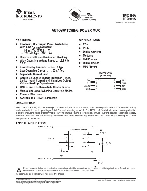
AVAILABLE OPTIONS Current Limit Adjustment Ranget − Time − 1 ms/divFigure 2 OUTPUT TURN-ON RESPONSEt − Time − 2 ms/divFigure 3C L = 1 µFC L = 0 µFt − Time − 40 µs/divFigure 475% less output voltagedroop compared to TPS2111t − Time − 250 µs/divFigure 6PACKAGING INFORMATIONOrderable Device Status (1)Package Type Package Drawing Pins Package Qty Eco Plan (2)Lead/Ball Finish MSL Peak Temp (3)TPS2110APW ACTIVE TSSOP PW 8150Green (RoHS &no Sb/Br)CU NIPDAU Level-1-260C-UNLIM TPS2110APWR ACTIVE TSSOP PW 82000Green (RoHS &no Sb/Br)CU NIPDAU Level-1-260C-UNLIM TPS2110APWRG4ACTIVE TSSOP PW 82000Green (RoHS &no Sb/Br)CU NIPDAU Level-1-260C-UNLIM TPS2111APW ACTIVE TSSOP PW 8150Green (RoHS &no Sb/Br)CU NIPDAU Level-1-260C-UNLIM TPS2111APWG4ACTIVE TSSOP PW 8150Green (RoHS &no Sb/Br)CU NIPDAU Level-1-260C-UNLIM TPS2111APWR ACTIVE TSSOP PW 82000Green (RoHS &no Sb/Br)CU NIPDAU Level-1-260C-UNLIM TPS2111APWRG4ACTIVETSSOPPW82000Green (RoHS &no Sb/Br)CU NIPDAULevel-1-260C-UNLIM(1)The marketing status values are defined as follows:ACTIVE:Product device recommended for new designs.LIFEBUY:TI has announced that the device will be discontinued,and a lifetime-buy period is in effect.NRND:Not recommended for new designs.Device is in production to support existing customers,but TI does not recommend using this part in a new design.PREVIEW:Device has been announced but is not in production.Samples may or may not be available.OBSOLETE:TI has discontinued the production of the device.(2)Eco Plan -The planned eco-friendly classification:Pb-Free (RoHS)or Green (RoHS &no Sb/Br)-please check /productcontent for the latest availability information and additional product content details.TBD:The Pb-Free/Green conversion plan has not been defined.Pb-Free (RoHS):TI's terms "Lead-Free"or "Pb-Free"mean semiconductor products that are compatible with the current RoHS requirements for all 6substances,including the requirement that lead not exceed 0.1%by weight in homogeneous materials.Where designed to be soldered at high temperatures,TI Pb-Free products are suitable for use in specified lead-free processes.Green (RoHS &no Sb/Br):TI defines "Green"to mean Pb-Free (RoHS compatible),and free ofBromine (Br)and Antimony (Sb)based flame retardants (Br or Sb do not exceed 0.1%by weight in homogeneous material)(3)MSL,Peak Temp.--The Moisture Sensitivity Level rating according to the JEDEC industry standard classifications,and peak solder temperature.Important Information and Disclaimer:The information provided on this page represents TI's knowledge and belief as of the date that it is provided.TI bases its knowledge and belief on information provided by third parties,and makes no representation or warranty as to the accuracy of such information.Efforts are underway to better integrate information from third parties.TI has taken and continues to take reasonable steps to provide representative and accurate information but may not have conducted destructive testing or chemical analysis on incoming materials and chemicals.TI and TI suppliers consider certain information to be proprietary,and thus CAS numbers and other limited information may not be available for release.In no event shall TI's liability arising out of such information exceed the total purchase price of the TI part(s)at issue in this document sold by TI to Customer on an annual basis.PACKAGE OPTION ADDENDUM17-Nov-2005Addendum-Page 1元器件交易网IMPORTANT NOTICETexas Instruments Incorporated and its subsidiaries (TI) reserve the right to make corrections, modifications,enhancements, improvements, and other changes to its products and services at any time and to discontinueany product or service without notice. Customers should obtain the latest relevant information before placingorders and should verify that such information is current and complete. All products are sold subject to TI’s termsand conditions of sale supplied at the time of order acknowledgment.TI warrants performance of its hardware products to the specifications applicable at the time of sale inaccordance with TI’s standard warranty. T esting and other quality control techniques are used to the extent TIdeems necessary to support this warranty. Except where mandated by government requirements, testing of allparameters of each product is not necessarily performed.TI assumes no liability for applications assistance or customer product design. Customers are responsible fortheir products and applications using TI components. T o minimize the risks associated with customer productsand applications, customers should provide adequate design and operating safeguards.TI does not warrant or represent that any license, either express or implied, is granted under any TI patent right,copyright, mask work right, or other TI intellectual property right relating to any combination, machine, or processin which TI products or services are used. Information published by TI regarding third-party products or servicesdoes not constitute a license from TI to use such products or services or a warranty or endorsement thereof.Use of such information may require a license from a third party under the patents or other intellectual propertyof the third party, or a license from TI under the patents or other intellectual property of TI.Reproduction of information in TI data books or data sheets is permissible only if reproduction is withoutalteration and is accompanied by all associated warranties, conditions, limitations, and notices. Reproductionof this information with alteration is an unfair and deceptive business practice. TI is not responsible or liable forsuch altered documentation.Resale of TI products or services with statements different from or beyond the parameters stated by TI for thatproduct or service voids all express and any implied warranties for the associated TI product or service andis an unfair and deceptive business practice. TI is not responsible or liable for any such statements.Following are URLs where you can obtain information on other Texas Instruments products and applicationsolutions:Products ApplicationsAmplifiers Audio /audioData Converters Automotive /automotiveDSP Broadband /broadbandInterface Digital Control /digitalcontrolLogic Military /militaryPower Mgmt Optical Networking /opticalnetworkMicrocontrollers Security /securityTelephony /telephonyVideo & Imaging /videoWireless /wirelessMailing Address:Texas InstrumentsPost Office Box 655303 Dallas, Texas 75265Copyright 2005, Texas Instruments Incorporated。
三菱PLC指令详解资料
一顺控指令1 触点指令00 LD 逻辑操作开始01 LDI 逻辑非操作开始02 AND 逻辑乘03 ANI 逻辑乘非04 OR 逻辑加05 ORI 逻辑加非2 连接指令06 ANB AND逻辑块与07 ORB OR逻辑块或08 MPS 存储操作结果09 MRD 从MPS读取操作结果10 MPP 从MPS读取操作结果并清除结果3 输出指令11 OUT 软元件输出12 SET 软元件置位13 RST 软元件复位14 PLS 在输入信号的上升沿15 PLF 在输入信号的下降沿16 CHK 软元件输出翻转4 移位指令17 SFT 元件移1位18 SFTP 元件移1位5 主控指令19 MC 主控开始20 MCR 主控复位6 结束指令21 FEND 结束主程序22 END 总的程序末尾,返回第0步7 其它指令23 STOP 停止24 NOP 空操作二基本指令1 比较指令16位数据比较25 LD= 当S1=S2, 接通,当S1≠S2, 断开26 AND=27 OR=28 LD<> 当S1≠S2, 接通,当S1=S2, 断开29 AND<>30 OR<>31 LD> 当S1>S2, 接通,当S1≤S2, 断开32 AND>33 OR>34 LD<= 当S1≤S2, 接通,当S1>S2, 断开35 AND<=36 OR<=37 LD< 当S1<S2, 接通,当S1≥S2, 断开38 AND<39 OR<40 LD>= 当S1≥S2, 接通,当S1<S2, 断开41 AND>=42 OR>=32位数据比较43 LDD= 当(S1+1,S1)=(S2+1,S2), 接通44 ANDD=45 ORD=46 LDD<> 当(S1+1,S1)≠(S2+1,S2),接通47 ANDD<>48 ORD<>49 LDD> 当(S1+1,S1)>(S2+1,S2), 接通50 ANDD>51 ORD>52 LDD<= 当(S1+1,S1)≤(S2+1,S2),接通53 ANDD<=54 ORD<=55 LDD< 当(S1+1,S1)<(S2+1,S2), 接通56 ANDD<57 ORD<58 LDD>= 当(S1+1,S1)≥(S2+1,S2),接通59 ANDD>=60 ORD>=2 算术运算指令二进制16位加/减61 + (D)+(S)→(D)62 +P63 + (S1)+(S2)→(D)64 +P65 - (D)-(S)→(D)66 -P67 - (S1)-(S2)→(D)68 -P二进制32位加/减69 D+ (D+1,D)+(S+1,S)→(D+1,D)70 D+P71 D+ (S1+1,S1)+(S2+1,S2)→(D+1,D)72 D+P73 D- (D+1,D)-(S+1,S)→(D+1,D)74 D-P75 D- (S1+1,S1)-(S2+1,S2)→(D+1,D)76 D-P77 * (S1)×(S2)→(D+1,D)78 *P79 / (S1)/(S2)→商(D), 余数(D+1)80 /P81 D* (S1+1,S1)×(S2+1,S2)→(D+3,D+2,D+1,D)82 D*P83 D/ (S1+1,S1)/(S2+1,S2)→商(D+1,D),余数(D+3,D+2)84 D/P85 B+ (D)+(S)→(D)86 B+P87 B+ (S1)+(S2)→(D)88 B+P89 B- (D)-(S)→(D)90 B-P91 B- (S1)-(S2)→(D)92 B-P93 DB+ (D+1,D)+(S+1,S) →(D+1,D)94 DB+P95 DB+ (S1+1,S1)+(S2+1,S2)→(D+1,D)96 DB+P97 DB- (D+1,D)-(S+1,S)→(D+1,D)98 DB-P99 DB- (S1+1,S1)-(S2+1,S2)→(D+1,D) 100 DB-P101 B* (S1)×(S2)→(D+1,D)102 B*P103 B/ (S1)/(S2)→商(D),余数(D+1)104 B/P105 DB* (S1+1,S1)×(S2+1,S2)→(D+3,D+2,D+1,D)106 DB*P107 DB/ (S1+1,S1)/(S2+1,S2)→商(D+1,D),余数(D+3,D+2) 108 DB/P109 INC (D)+1→(D)110 INCP111 DINC (D+1,D)+1→(D+1,D) 112 DINCP113 DEC (D)-1→(D)114 DECP115 DDEC (D+1,D)-1→(D+1,D) 116 DDECP3 BCD—二进制转换117 BCD (S)→(D)BCD转换118 BCDP119 DBCD (S+1,S)→(D+1,D) 120 DBCDP121 BIN (S)→(D)二进制转换122 BINP123 DBIN (S+1,S)→(D+1,D) 124 DBINP4 数据传送指令125 MOV (S)→(D)126 MOVP127 DMOV (S+1,S)→(D+1,D)128 DMOVP129 CML (S)→(D)130 CMLP131 DCML (S+1,S)→(D+1,D)132 DCML133 DCMLP134 BMOV (S)→(D)n个135 BMOVP136 FMOV (S)→(D)n个137 FMOVP138 XCH (D1)←→(D2)139 XCHP140 DXCH (D1+1,D1)←→(D2+1,D2) 141 DXCHP5 程序分支指令142 CJ 条件满足,跳转到P**处143 SCJ 条件满足后紧接的扫描周期, 跳转到P**处144 JMP 无条件跳转到P**处145 CALL 执行P**处子程序146 CALLP147 RET 从子程序返回148 EI 允许中断149 DI 禁止中断150 IRET 从中断程序返回151 SUB 执行n指定的程序152 SUBP6 程序切换指令153 CHG 在主副程序间切换7 刷新指令154 COM 执行通讯刷新155 EI 允许通讯刷新156 DI 禁止通讯刷新157 SEG 对应软元件的刷新,仅执行1个扫描周期,M9052 O N时有效三应用指令1 逻辑运算指令158 WAND (D) AND (S)→(D)159 WANDP160 WAND (S1) AND (S2)→(D)161 WANDP162 DAND (D+1,D) AND (S+1,S)→(D+1,D) 163 DANDP164 WOR (D) OR (S)→(D)165 WORP166 WOR (S1) OR (S2)→(D)167 WORP168 DOR (D+1,D) OR (S+1,S)→(D+1,D) 169 DORP170 WXOR (D) XOR (S)→(D)异或171 WXORP172 WXOR (S1) XOR (S2)→(D)173 WXORP174 DXOR (D+1,D) XOR (S+1,S)→(D+1,D) 175 DXORP176 WXNR (D) XOR (S)→(D)177 WXNRP178 WXNR (S1) XOR (S2)→(D)179 WXNRP180 DXNR (D+1,D) XOR (S+1,S)→(D+1,D) 181 DXNRP182 NEG 0-(D)→(D)补码183 NEGP2 旋转指令184 ROR n位右转185 RORP186 RCR n位右转(带进位) 187 RCRP188 ROL n位左转189 ROLP190 RCL n位左转(带进位) 191 RCLP192 DROR n位右转193 DRORP194 DRCR n位右转(带进位) 195 DRCRP196 DROL n位左转197 DROLP198 DRCL n位左转(带进位) 199 DRCLP3 移位指令200 SFR n位右移201 SFRP202 SFL n位左移203 SFLP204 BSFR 1位右移205 BSFRP206 BSFL 1位左移207 BSFLP208 DSFR 1位右移209 DSFRP210 DSFL 1位左移211 DSFLP4 数据处理指令212 SER 数据搜索213 SERP214 SUM 位检查215 SUMP216 DSUM217 DSUMP218 DECO 译码编码219 DECOP220 ENCO221 ENCOP222 SEG 7段编码223 BSET 对字中n位置位224 BSETP225 BRST 对字中n位复位226 BRSTP227 DIS 组合分离228 DISP229 UNI230 UNIP231 ASC ASCII转化5 先进先出指令232 FIFW FIFO写233 FIFWP234 FIFR FIFO读235 FIFRP6 内存缓冲区存取指令236 FROM 从特殊功能模块读取数据237 FROMP238 DFRO239 DFROP240 TO 向特殊功能模块写数据241 TOP242 DTO243 FROM 从远程I/O站读数据244 FROMP245 DFRO246 DFROP247 TO 向远程站写数据248 TOP249 DTO250 DTOP7 FOR/NEXT指令251 FOR 重复n次252 NEXT8 本地站、远程I/O站存取指令253 LRDP 从本地站读数据254 LWTP 向本地站写数据255 RFRP 从远程特殊功能模块读数据256 RTOP 向远程特殊功能模块写数据9 显示指令257 PR 从指定的8点字软元件输出16个字符的ASCII码258 PR 顺序向输出模块输出ASCII 码, 直到结束符NUL(00H)259 PRC 将字软元件的注释转换成 ASCII码,并输出260 LED 将指定的8点字软元件显示16个字符的ASCII码261 LEDA 显示指定的英文数字字符262 LEDB263 LEDC 显示软元件S的注释264 LEDR 显示复位10 其它指令265 WDT WDT复位266 WDTP267 CHK 故障检测268 SLT 按参数设定的条件,数据被锁定269 SLTR 状态锁存复位,且执行SLT 270 STRA 按参数设定的条件,采样数据存入271 STRAR 采样跟踪复位,且允许执行272 STC 进位标志(M9012)ON273 CLC 进位标志(M9012)OFF274 DUTY 用户定义时钟11 伺服指令275 DSFRP 请求启动伺服程序276 PSFLP 数据修改特殊继电器和特殊寄存器一特殊继电器M清单M9000 熔丝断M9002 I/O组件校验出错M9004 MINI网通讯出错M9005 AC电源掉电检测M9006 电池电压低M9007 电池电压低锁存M9008 自诊断出错M9009 信号报警器检测M9010 运算出错标志M9011 运算出错标志锁存M9012 进位标志M9016 数据存储区清零标志M9017 数据存储区清零标志M9018 数据通讯监控切换M9020 0号用户定时时钟M9021 1号用户定时时钟M9022 2号用户定时时钟M9023 3号用户定时时钟M9024 4号用户定时时钟M9025 时钟数据设置请求M9026 时钟数据出错M9027 时钟数据显示M9028 时钟数据读请求M9030 0.1秒时钟M9031 0.2秒时钟M9032 1秒时钟M9033 2秒时钟M9034 1分钟时钟M9036 常开M9037 常闭M9038 RUN后第一个扫描周期ON M9039 运行标志M9040 暂停PAUSE允许线圈M9041 PAUSE状态触点M9042 停止状态触点M9043 采样跟踪完成M9044 采样跟踪M9046 采样跟踪M9047 采样跟踪准备M9048 RUN LED闪烁标志M9049 切换输出字符数目M9050 存放操作结果的存储区交换触点M9051 CHG指令执行禁止M9052 SEG指令切换M9053 EI/DI指令切换M9054 单步运行标志M9055 状态锁存完成标志M9056 主程序P, I设置请求M9057 副程序P, I设置程序M9060 副程序2P, I设置程序M9061 副程序3P, I设置程序M9060 远程终端出错M9061 通讯出错M9065 分离传送状态M9066 传送处理切换M9067 I/O组件出错检测M9068 测试模式M9069 线路故障时的输出M9073 WDT出错标志M9074 PCPU准备完成标志M9075 测试模式标志M9076 外部急停输入标志M9077 手动脉冲发生器轴设置错误标志M9078 测试模式请求出错标志M9079 伺复程序设置出错标志M9081 对远程模块的通讯请求M9082 最终站数不一致M9084 出错检测M9086 运行标志BASIC程序M9087 暂停(PAUSE)标志M9091 操作运行出错细节标志M9091 微机子程序调用出错标志M9092 双电源模块过热M9093 双工电源模块出错M9094 I/O改变标志M9095 双工运行校验出错M9096 A3VCPU A自校出错M9097 A3VCPU B自校出错M9098 A3VCPU C自校出错M9099 A3VTU自校出错M9100 SFC程序登记M9101 SFC程序起/停M9102 SFC启动状态M9103 连续步转移有效/失效M9104 连续转移防止标志M9108 步转移监控定时器起始 (对应D9108)M9109 步转移监控定时器起始 (对应D9109)M9110 步转移监控定时器起始 (对应D9110)M9111 步转移监控定时器起始 (对应D9111)M9112 步转移监控定时器起始 (对应D9112)M9113 步转移监控定时器起始 (对应D9113)M9114 步转移监控定时器起始 (对应D9114)M9180 激活步采样跟踪完成标志M9181 激活步采样跟踪执行标志M9182 激活步采样跟踪有效M9196 在块停止时控制输出M9197~9198 保险丝熔断,I/O校核出错显示切换二特殊寄存器D9000 保险丝断D9001 保险丝断D9002 I/O组件校验出错D9003 SUM指令检测位数D9004 MINI网主通讯组件出错D9005 AC掉电计数D9006 电池不足D9008 自诊断出错D9009 信号报警器检测D9010 出错步D9011 出错步D9014 I/O控制模式D9015 CPU运行状态D9016 ROM/RAM设置D9017 最小扫描时间D9018 当前扫描时间D9019 最大扫描时间D9020 恒定扫描D9021 扫描时间D9022 1秒计数器D9025 时钟数据(年,月)D9026 时钟数据(日,时)D9027 时钟数据(分,秒)D9028 时钟数据(星期)D9021~D9034 远程终端组件参数设置D9035 远程I/O组件的通讯属性D9035 扩展文件寄存器D9036 总的站数D9036~9037 供指定扩展文件寄存器软件地址D9038~9039 LED显示优先级D9044 采样跟踪D9050 SFC程序出错代码D9051 出错块D9052 出错步D9053 转移出错D9054 出错顺控步D9055 状态锁存步序号D9061 通讯出错代码D9072 PC通讯检测D9081 对远程终端模块的已执行的通讯请求数D9082 最后的站号D9090 微机子程序输入数据区首软元件号D9091 指令出错D9094 待更换的I/O组件的首地址D9095 A3VTS系统和A3VCPU的运行状态D9096 A3VCPU A自检出错D9097 A3VCPU B自检出错D9098 A3VCPU C自检出错D9099 A3VTU 自检测出错D9100~D9107 断保险丝的组件D9100 保险丝熔断的组件D9108~D9114 步转移监控定时器设置D9116~D9123 I/O组件校验出错D9124 信号器报警数量检测D9125~D9132 信号报警器地址号D9133~D9140 远程终端卡信息D9141~D9172 通讯重发次数D9173 模式设置D9174 设置重发次数D9175 线缆出错模块出错代码D9180~9193远程终端模块出错代码D9180 轴1和轴2的限位开关输出状态存储区D9181 轴3和轴4的限位开关输出状态存储区D9182 轴5和轴6的限位开关输出状态存储区D9183 轴7和轴8的限位开关输出状态存储区D9184 CPU出错的原因D9185 伺服放大器接线数据D9187 手动脉冲发生器轴设置出错D9188 在TEST模式下启动轴号请求出错D9189 出错程序号D9190 数据设置出错D9191 伺服放大器类型D9196~9199 故障站检测D9200 LRDP处理结果D9201 LWTP处理结果D9204 通讯状态D9205 执行回送的站D9206 执行回送的站D9207 通讯扫描时间(最大值)D9208 通讯扫描时间(最小值)D9209 通讯扫描时间(当前值)D9210 重发次数D9211 环路切换计数D9212 就地站运行状态(1~16)D9213 就地站运行状态(17~32)D9214 就地站运行状态(33~48)D9215 就地站运行状态(49~64)D9216 就地站出错检测(1~16)D9217 就地站出错检测(17~32)D9218 就地站出错检测(33~48)D9219 就地站出错检测(49~64)D9220 就地站参数不匹配或(1~16)远程站I/O分配出错D9221 就地站参数不匹配或(17~32)远程站I/O分配出错D9222 就地站参数不匹配或(33~48)远程站I/O分配出错D9223 就地站参数不匹配或(49~64)远程站I/O分配出错D9224 主站与从站和远程I/O站之间的初始通讯(1~16)D9225 主站与从站和远程I/O站之间的初始通讯(17~32)D9226 主站与从站和远程I/O站之间的初始通讯(33~48)D9227 主站与从站和远程I/O站之间的初始通讯(49~64)D9228 就地站或远程I/O站出错(1~16)D9229 就地站或远程I/O站出错(17~32) D9230 就地站或远程I/O站出错(33~48) D9231 就地站或远程I/O站出错(49~64) D9232 就地站或远程I/O站环路出错D9233 就地站或远程I/O站环路出错D9234 就地站或远程I/O站环路出错D9235 就地站或远程I/O站环路出错D9236 就地站或远程I/O站环路出错D9237 就地站或远程I/O站环路出错D9238 就地站或远程I/O站环路出错D9239 就地站或远程I/O站环路出错D9240 检测到接收出错的次数D9243 本站站号检测D9244 从站的总数D9245 检测到的接收出错次数D9248 就地站运行状态D9249 就地站运行状态D9250 就地站运行状态D9251 就地站运行状态D9252 就地站出错检测D9253 就地站出错检测D9254 就地站出错检测D9255 就地站出错检测各种软元件一览表项目 A1,A1NA1S A2,A2NA2C A2-S1A2N-S1 A3,A3NA3A A 2U,A3UA4UI/O软元件点 256 512 1024 2048 8192输入继电器 X 0~FF 0~1FF 0~3FF 0~7FF 0~FFF输出继电器 Y 0~FF 0~1FF 0~3FF 0~7FF 0~FFF辅助继电器内部继电器 (1000点)M0~M999 M0~M999, M2 048~8191特殊继电器 (256点)M9000~M9255锁存继电器 (1048点)L1000~L2048通讯用继电器 (2048点)B0~B3FF B0~BFFF定时器 100ms定时器 (200点)T0~T19910ms定时器 (56点)T200~T255100ms记忆定时器 (0点)计数器 (256点)C0~C255寄存器数据寄存器 (1024点)D0~D1023 D0~D6143特殊寄存器 (256点)D9000~D9255通讯寄存器 (1024点)W0~W3FF W0~WFFF累加器 (2点)A0,A1变址寄存器 (2点)Z, V Z,Z1~Z6(7点), V,V1~V6(7点) 嵌套 (8点)N0~ N7指针 (256点)P0~P255中断指针 (32点)I0~I31常数十进制 K (16位)-32768~+32767(32位)-2147483648 ~+2147483647十六进制 H (16位)0~FFFF(32位)0~FFFFFFFF。
示教器TP1说明书
机器人控制器选件示教器 TP1 Rev.8机器人控制器选件示教器TP1Rev.8Copyright © 2012-2021 SEIKO EPSON CORPORATION. All rights reserved. TP1 Rev.8i前言感谢您购买本公司的机器人系统。
本手册记载了正确使用示教器所需的事项。
使用系统之前,请阅读本手册与相关手册,正确地进行使用。
阅读之后,请妥善保管,以便随时取阅。
本公司的产品均通过严格的测试和检查,以确保机器人系统的性能符合本公司的标准。
但是如果在超出本手册所描述的环境中使用本产品,则可能会影响产品的基本性能。
本手册阐述了本公司可以预见的危险和问题。
请务必遵守本手册中的安全注意事项,安全正确地使用机器人系统。
商标Microsoft、Windows、Windows商标,为美国Microsoft Corporation在美国与其它国家的注册商标或商标。
其它品牌与产品名称均为各公司的注册商标或商标。
本手册中的商标符号Microsoft® Windows® 8 Operating systemMicrosoft® Windows® 10 Operating system在本手册中,Windows 8和Windows 10指的是上述各操作系统。
在某些情况下,Windows一般是指Windows 8和Windows 10。
注意事项禁止擅自复印或转载本手册的部分或全部内容。
本手册记载的内容将来可能会随时变更,恕不事先通告。
如您发现本手册的内容有误或需要改进之处,请不吝斧正。
制造商联系方式有关咨询处的详细内容,请参阅下记手册序言中的“销售商”。
机器人系统安全手册请首先阅读本手册ii TP1 Rev.8TP1 Rev.8 iii阅读本手册之前本手册将以这些符号表示下述说明。
描述了操作机器人系统时需要注意和了解的事项。
介绍简单的操作方法和操作技巧。
SPS-9110AFWG中文资料
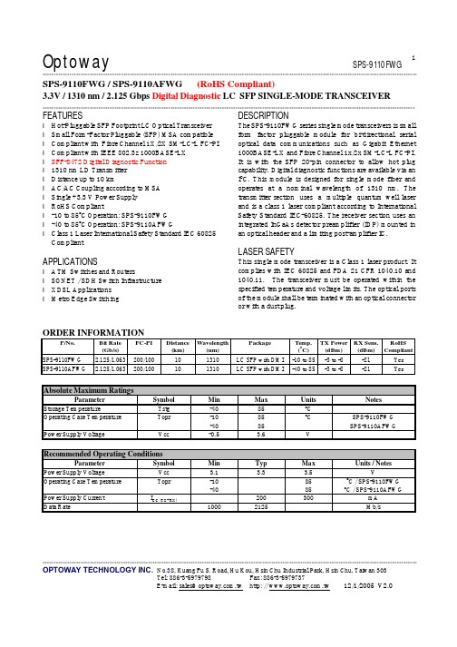
Optoway SPS-9110FWG**********************************************************************************************************************************************************************************************************************************************************************************************************************************************OPTOWAY TECHNOLOGY INC. No .38, Kuang Fu S. Road, Hu Kou, Hsin Chu Industrial Park, Hsin Chu, Taiwan 303Tel: 886-3-5979798 Fax: 886-3-5979737E-mail: sales@ http: // 12/1/2005 V2.01SPS-9110FWG / SPS-9110AFWG (RoHS Compliant)3.3V / 1310 nm / 2.125 Gbps Digital Diagnostic LC SFP SINGLE-MODE TRANSCEIVER **********************************************************************************************************************************************************************FEATURESl Hot-Pluggable SFP Footprint LC Optical Transceiver l Small Form-Factor Pluggable (SFP) MSA compatible l Compliant with Fibre Channel 1X/2X SM-LC-L FC-PI l Compliant with IEEE 802.3z 1000BASE-LX l SFF-8472 Digital Diagnostic Function l 1310 nm LD Transmitter l Distance up to 10 kml AC/AC Coupling according to MSA l Single +3.3 V Power Supply l RoHS Compliantl -10 to 85o C Operation: SPS-9110FWG l -40 to 85o C Operation: SPS-9110AFWGl Class 1 Laser International Safety Standard IEC 60825 CompliantAPPLICATIONSl ATM Switches and Routersl SONET / SDH Switch Infrastructure l XDSL Applications l Metro Edge SwitchingDESCRIPTIONThe SPS-9110FWG series single mode transceivers is small form factor pluggable module for bi-directional serial optical data communications such as Gigabit Ethernet 1000BASE-LX and Fibre Channel 1x/2x SM-LC-L FC-PI. It is with the SFP 20-pin connector to allow hot plug capability. Digital diagnostic functions are available via an I 2C. This module is designed for single mode fiber and operates at a nominal wavelength of 1310 nm. The transmitter section uses a multiple quantum well laser and is a class 1 laser compliant according to International Safety Standard IEC-60825. The receiver section uses an integrated InGaAs detector preamplifier (IDP) mounted in an optical header and a limiting post-amplifier IC.LASER SAFETYThis single mode transceiver is a Class 1 laser product. It complies with IEC 60825 and FDA 21 CFR 1040.10 and 1040.11. The transceiver must be operated within the specified temperature and voltage limits. The optical ports of the module shall be terminated with an optical connector or with a dust plug.ORDER INFORMATIONP/No. Bit Rate (Gb/s) FC-PI Distance (km) Wavelength (nm) Package Temp.(o C) TX Power (dBm) RX Sens. (dBm) RoHS Compliant SPS-9110FWG 2.125/1.063 200/100 10 1310 LC SFP with DMI -10 to 85 -3 to -8 -21 Yes SPS-9110AFWG2.125/1.063200/100101310LC SFP with DMI-40 to 85-3 to -8-21YesAbsolute Maximum RatingsParameterSymbol Min Max Units NotesStorage TemperatureTstg -40 85 o COperating Case Temperature Topr -10 -40 85 85 o C SPS-9110FWG SPS-9110AFWG Power Supply VoltageVcc-0.53.6VRecommended Operating ConditionsParameterSymbol Min Typ Max Units / NotesPower Supply VoltageVcc 3.1 3.3 3.5 VOperating Case Temperature Topr -10 -40 85 85 oC / SPS-9110FWG oC / SPS-9110AFWGPower Supply Current I CC (TX+RX)200 300 mA Data Rate10002125Mb/s***********************************************************************************************************************************************************************OPTOWAY TECHNOLOGY INC. No .38, Kuang Fu S. Road, Hu Kou, Hsin Chu Industrial Park, Hsin Chu, Taiwan 303Tel: 886-3-5979798 Fax: 886-3-5979737Transmitter Specifications (-10o C < Topr < 85o C, 3.1V < Vcc < 3.5V)ParameterSymbolMinTypMaxUnits Notes OpticalOptical Transmit Power Po -8 --- -3 dBm 1Output Center Wavelength λ 1270 1310 1350 nmOutput Spectrum Width ∆λ --- --- 2.5 nm RMS (σ) Extinction Ratio E R 9 --- dBOptical Modulation Amplitude (Peak-to-Peak) OMA 174 µW FC-PI Standard Optical Rise Time t r 160 ps 20 % to 80% Values Optical Fall Time t f 160 ps 20 % to 80% Values Relative Intensity Noise RIN -120 dB/HzElectricalData Input Current – Low I IL -350 µA Data Input Current – High I IH 350 µADifferential Input Voltage V IH - V IL 0.5 2.4 V Peak-to-PeakTX Disable Input Voltage – Low T DIS, L 0 0.5 V 2 TX Disable Input Voltage – High T DIS, H 2.0 Vcc V 2 TX Disable Assert Time T ASSERT 10 µs TX Disable Deassert Time T DEASSERT 1 ms TX Fault Output Voltage -- Low T FaultL 0 0.8 V 3 TX Fault Output Voltage -- High T FaultH 2.0 Vcc+0.3 V31. Output power is power coupled into a 9/125 µm single mode fiber.2. There is an internal 4.7K to 10K ohm pull-up resistor to VccTX.3. Open collector compatible,4.7K to 10K ohm pull-up to Vcc (Host Supply Voltage).Receiver Specifications (-10o C < Topr < 85o C, 3.1V < Vcc < 3.5V)ParameterSymbol Min Typ Max Units NotesOpticalSensitivity @2.125Gb/s @ BER=10-12 SENS (2X) --- --- -21 dBm 4 Sensitivity @1.25Gb/s @ BER=10-12SENS (1X)-22 dBm 4 Maximum Input Power Pin -3 dBm 4Signal Detect -- Asserted Pa --- -21 dBm Transition: low to high Signal Detect -- Deasserted Pd -30 --- --- dBm Transition: high to low Signal detect -- Hysteresis 1.0 --- dBWavelength of Operation1100---1600nmElectricalDifferential Output Voltage V OH – V OL 0.6 2.0 V Output LOS Voltage -- Low V OL 0 0.8 V 5 Output LOS Voltage -- High V OH 2.0 Vcc+0.3V54. Measured at 27-1 PRBS at BER 1E-12 @ 1300 nm.5. Open collector compatible, 4.7K to 10K ohm pull-up to Vcc (Host Supply Voltage).***********************************************************************************************************************************************************************OPTOWAY TECHNOLOGY INC. No .38, Kuang Fu S. Road, Hu Kou, Hsin Chu Industrial Park, Hsin Chu, Taiwan 303Tel: 886-3-5979798 Fax: 886-3-5979737PINSignal NameDescriptionPINSignal Name Description1 TX GND Transmitter Ground11 RX GND Receiver Ground2 TX Fault Transmitter Fault Indication12 RX DATA OUT- Inverse Receiver Data Out 3 TX Disable Transmitter Disable (Module disables on high or open)13 RX DATA OUT+ Receiver Data Out 4 MOD-DFE2 Modulation Definition 2 – Two wires serial ID Interface14 RX GND Receiver Ground5 MOD-DEF1 Modulation Definition 1 – Two wires serial ID Interface15 Vcc RX Receiver Power – 3.3V ±5% 6 MOD-DEF0 Modulation Definition 0 – Ground in Module16 Vcc TX Transmitter Power – 3.3V ±5% 7 N/C Not Connected 17 TX GNDTransmitter Ground 8 LOS Loss of Signal 18 TX DATA IN+ Transmitter Data In9 RX GND Receiver Ground 19 TX DATA IN- Inverse Transmitter Data In 10RX GNDReceiver Ground20TX GNDTransmitter GroundModule DefinitionModule DefinitionMOD-DEF2 PIN 4 MOD-DEF1 PIN 5 MOD-DEF0 PIN 6 Interpretation by Host 4SDASCLLV-TTL LowSerial module definitionprotocolModule Definition 4 specifies a serial definition protocol. For this definition, upon power up, MOD-DEF(1:2) appear as no connector (NC) and MOD-DEF(0) is TTL LOW. When the host system detects this condition, it activates the serial protocol. The protocol uses the 2-wire serial CMOS E 2PROM protocol of the ATMEL AT24C01A/02/04 family of components.*********************************************************************************************************************************************************************** OPTOWAY TECHNOLOGY INC. No.38, Kuang Fu S. Road, Hu Kou, Hsin Chu Industrial Park, Hsin Chu, Taiwan 303Tel: 886-3-5979798 Fax: 886-3-5979737。
UN9111资料

* hFE rank classification (UN9115/9116/9117/9110)
Rank hFE Q 160 to 260 R 210 to 340 S 290 to 460
2
元器件交易网
UN9111/9112/9113/9114/9115/9116/9117/9118/9119/9110/ Transistors with built-in Resistor 911D/911E/911F/911H/911L/UNR911AJ/911BJ/911CJ
UN9111/9112/9113/9114/9115/9116/9117/9118/9119/9110/ Transistors with built-in Resistor 911D/911E/911F/911H/911L/UNR911AJ/911BJ/911CJ
s Electrical Characteristics
Cob — VCB
6
IO — VIN
f=1MHz IE=0 Ta=25˚C
VIN — IO
VO=–5V Ta=25˚C
–100 –30 VO= –0.2V Ta=25˚C
–10000 –3000
Collector output capacitance Cob (pF)
5
Output current IO (µA)
–160 –140 IB=–1.0mA Ta=25˚C –100
VCE(sat) — IC
Collector to emitter saturation voltage VCE(sat) (V)
IC/IB=10 160 VCE= –10V
hFE — IC
Ta=75˚C
HP-UX11使用手册_中文

- 1、下载文档前请自行甄别文档内容的完整性,平台不提供额外的编辑、内容补充、找答案等附加服务。
- 2、"仅部分预览"的文档,不可在线预览部分如存在完整性等问题,可反馈申请退款(可完整预览的文档不适用该条件!)。
- 3、如文档侵犯您的权益,请联系客服反馈,我们会尽快为您处理(人工客服工作时间:9:00-18:30)。
CHIP THICKNESS:15 TYPICAL BONDING PADS:3.3 × 3.3 MINIMUM T J max = 150°C
TOLERANCES ARE ±10%.ALL DIMENSIONS ARE IN MILS.
153
94
4
12
25
26
5
6
7
8
9
10
11
13
14
15
16
17
24
23
22
21
20
19
18
27
28
12
3
BONDING PAD ASSIGNMENTS
元器件交易网
IMPORTANT NOTICE
Texas Instruments (TI) reserves the right to make changes to its products or to discontinue any semiconductor
product or service without notice, and advises its customers to obtain the latest version of relevant information
to verify, before placing orders, that the information being relied on is current.
TI warrants performance of its semiconductor products and related software to the specifications applicable at
the time of sale in accordance with TI’s standard warranty. Testing and other quality control techniques are
utilized to the extent TI deems necessary to support this warranty. Specific testing of all parameters of each
device is not necessarily performed, except those mandated by government requirements.
Certain applications using semiconductor products may involve potential risks of death, personal injury, or
severe property or environmental damage (“Critical Applications”).
TI SEMICONDUCTOR PRODUCTS ARE NOT DESIGNED, INTENDED, AUTHORIZED, OR WARRANTED
TO BE SUITABLE FOR USE IN LIFE-SUPPORT APPLICATIONS, DEVICES OR SYSTEMS OR OTHER
CRITICAL APPLICATIONS.
Inclusion of TI products in such applications is understood to be fully at the risk of the customer. Use of TI
products in such applications requires the written approval of an appropriate TI officer. Questions concerning
potential risk applications should be directed to TI through a local SC sales office.
In order to minimize risks associated with the customer’s applications, adequate design and operating
safeguards should be provided by the customer to minimize inherent or procedural hazards.
TI assumes no liability for applications assistance, customer product design, software performance, or
infringement of patents or services described herein. Nor does TI warrant or represent that any license, either
express or implied, is granted under any patent right, copyright, mask work right, or other intellectual property
right of TI covering or relating to any combination, machine, or process in which such semiconductor products
or services might be or are used.
Copyright © 1996, Texas Instruments Incorporated。