RX Noise Figure
T7026中文资料

Features•Single 3-V Supply Voltage•High-power-added Efficient Power Amplifier (P out Typically 28dBm)•Ramp-controlled Output Power•Low-noise Preamplifier (NF Typically 2.1dB)•Biasing for External PIN Diode T/R Switch •Current-saving Standby Mode •Few External Components •Package: QFN20DescriptionThe T7026 is a monolithic SiGe transmit/receive front-end IC with power amplifier,low-noise amplifier and T/R switch driver. It is especially designed for operation in TDMA systems like DECT, IEEE 802.11 FHSS WLAN, home RF and ISM proprietary radios. Due to the ramp-control feature and a very low quiescent current, an external switch transistor for V S is not required.Electrostatic sensitive device.Observe precautions for handling.Figure 1. Block Diagram2T70264563C–ISM–01/04Pin ConfigurationFigure 2.Pinning QFN20Pin DescriptionPin Symbol Function 1RX_ON RX active high2R_SWITCH Resistor to GND sets the PIN diode current3SWITCH_OUT_RX Switched current output for PIN diode (active in RX mode)4SWITCH_OUT_TXSwitched current output for PIN diode (active in TX mode)5GND_LNA1Ground6LNA_IN Low-noise amplifier input 7GND_LNA2Ground8V3_P A_OUT Inductor to power supply and matching network for power amplifier output 9V3_P A_OUT Inductor to power supply and matching network for power amplifier output 10V3_P A_OUT Inductor to power supply and matching network for power amplifier output 11V2_P A Inductor to power supply for power amplifier 12V2_P A Inductor to power supply for power amplifier 13GND Ground14V1_P A Supply voltage for power amplifier 15NC Not connected16RAMP Power ramping control input 17P A_IN Power amplifier input18VS_LNA Supply voltage input for low-noise amplifier 19LNA_OUTLow-noise amplifier output 20PU Power-up active high SlugGNDGround3T70264563C–ISM–01/04Absolute Maximum RatingsStresses beyond those listed under “Absolute Maximum Ratings” may cause permanent damage to the device. This is a stress rating only and functional operation of the device at these or any other conditions beyond those indicated in the operational sections of this specification is not implied. Exposure to absolute maximum rating conditions for extended periods may affect device reliability.All voltages are referred to ground (pins GND and slug)ParametersSymbol Value Unit Supply voltagePins VS_LNA, V1_P A, V2_P A and V3_P A_OUT, no RF V S 5V Junction temperature T j 150°C Storage temperature T stg -40 to +125°C RF input power LNA P inLNA -5 dBm dBm RF input power P AP inPA10 dBmdBmThermal ResistanceParametersSymbol Value Unit Junction ambient QFN20, slug soldered on PCBR thJA27K/WOperating RangeAll voltages are referred to ground (pins GND and slug). Power supply points are VS_LNA, V1_P A, V2_P A, V3_P A_OUT. The following table represents the sum of all supply currents depending on the TX/RX mode.ParametersSymbol Min.Typ.Max.Unit Supply voltagePins V1_P A, V2_P A and V3_P A_OUT V S 2.7 3.6 4.6V Supply voltage Pin VS_LNA V S 2.73.0 5.5V Supply currentTX RXI S I S 4708mA mA Standby current PU = 0I S 10µAAmbient temperatureT amb-25+25+70°C4T70264563C–ISM–01/04Electrical CharacteristicsTest conditions (unless otherwise specified): V S = 3.6 V , T amb = 25°CParameters Test Conditions Symbol Min.Typ.Max.UnitPower Amplifier (1)Supply voltage Pins V1_P A, V2_P A and V3_P A_OUT V S 2.7 3.6 4.6V Supply current TXI S_TX 470mARX (P A off), V RAMP £ 0.1 V I S_RX 10µA Standby current Standby for V RAMP £ 0.1V I S_standby10µA Frequency range TX f 2.4 2.5GHz Gain-control range TXD Gp 6042dB Power gain maximum TXPin P A_IN to V3_P A_OUT Gp 283433dB Power gain minimum Gp -40-17dB Ramping voltage maximum TX, power gain (max), pin RAMP V RAMP max 1.61.65 1.7V Ramping voltage minimum TX, power gain (min), pin RAMP V RAMP min 1V Ramping current maximum TX, V RAMP = 1.75 V , pin RAMP I RAMP max 0.1mA Power-added efficiency TXP AE 3337%Saturated output power TX, input power = 0 dBm referred to pins V3_P A_OUT P sat 272829dBmInput matching (2)TX pin P A_IN Load VSWR < 1.5:1Output matching (2)TX pins V3_P A_OUT Load VSWR < 1.5:1Harmonics at P 1dBCP TX pins V3_P A_OUT 2 fo -30dBc Harmonics at P 1dBCPTX pins V3_P A_OUT 3 fo -30dBc T/R-switch Driver (Current Programming by External Resistor from R_SWITCH to GND)Switch-out current outputStandby, pin SWITCH_OUT I S_O_standby 1µA RXI S_O_RX 1µA TX at 100 W I S_O_100 1.7mA TX at 1.2 k W I S_O_1k27mA TX at 33 k W I S_O_33k 17mA TX at R switch openI S_O_R19mA I_Switch_Out_RX maximum7mA Low-noise Amplifier (3)Supply voltage All, pin VS_LNA V S 2.73.05V Supply current RXI S 810mA Supply current(LNA and control logic)TX (control logic active)pin VS_LNAI S 0.5mA Standby current Standby, pin VS_LNA I S_standby110µA Frequency range RXf2.42.5GHzNotes:1.Power amplifier shall be unconditionally stable, maximum duty cycle 100%, true cw operation, maximum load mismatchand duration: VSWR = 8:1 (all phases) 10 s, ZG = 50 W , V S = 3.6 V . 2.With external matching network, load impedance 50 W .3.Low-noise amplifier shall be unconditionally stable.4.With external matching components.5T70264563C–ISM–01/04Power gain RX, pin LNA_IN to LNA_OUT Gp 151619dB Noise figure RXNF 2.1 2.3dB Gain compressionRX, referred to pin LNA_OUT O1dB -9-7-6dBm Third-order input interception point RXIIP3-16-14-13dBmInput matching (4)RX, pin LNA_IN VSWRin < 2:1Output matching (4)RX, pin LNA_OUT VSWRout< 2:1Logic Input Levels (RX_ON, PU)High input level = ‘1’, pins RX_ON and PU V iH 2.4V S, LNA V Low input level = ‘0’V iL 00.5V High input current = ‘1’, V iH = 2.4V I iH 4060µA Low input current = ‘0’I iL0.2µAElectrical Characteristics (Continued)Test conditions (unless otherwise specified): V S = 3.6 V , T amb = 25°CParameters Test ConditionsSymbol Min.Typ.Max.Unit Notes:1.Power amplifier shall be unconditionally stable, maximum duty cycle 100%, true cw operation, maximum load mismatchand duration: VSWR = 8:1 (all phases) 10 s, ZG = 50 W , V S = 3.6 V . 2.With external matching network, load impedance 50 W .3.Low-noise amplifier shall be unconditionally stable.4.With external matching components.Control Logic for LNA and T/R-switch DriverOperation Mode PU RX_ON Standby 00TX 10RX116T70264563C–ISM–01/04Input/Output CircuitsFigure 3. Internal Circuitry; PA_IN, V1_PAFigure 4. Internal Circuitry; RAMP, V1_PAFigure 5. Internal Circuitry V2_PAPA_INV1_PAGNDV1_PARAMPV2_PAGND7T70264563C–ISM–01/04Figure 6. Internal Circuitry V3_PA_OUTFigure 7. Internal Circuitry SWITCH_OUT_RX, SWITCH_OUT_TX, R_SWITCH,V1_PAFigure 8. Internal Circuitry LNA_IN, VS_LNAV3_PA_OUTGNDV1_PAGNDSWITCH_OUT_RX/SWITCH_OUT_TXR_SWITCHVS_LNAGNDLNA_IN8T70264563C–ISM–01/04Figure 9. Internal Circuitry PU, RX_ON, VS_LNAFigure 10. Internal Circuitry LNA_OUT, VS_LNAVS_LNARX_ON/ PUVS_LNAGNDLNA_OUT9T70264563C–ISM–01/04Package InformationOrdering InformationExtended Type Number Package Remarks T7026-PGS QFN20TubeT7026-PGQ QFN20Taped and reeled T7026-PGPQFN20Taped and reeledDisclaimer: Atmel Corporation makes no warranty for the use of its products, other than those expressly contained in the Company’s standard warranty which is detailed in Atmel’s Terms and Conditions located on the Company’s web site. The Company assumes no responsibility for any errors which may appear in this document, reserves the right to change devices or specifications detailed herein at any time without notice, and does not make any commitment to update the information contained herein. No licenses to patents or other intellectual property of Atmel are granted by the Company in connection with the sale of Atmel products, expressly or by implication. Atmel’s products are not authorized for use as critical components in life support devices or systems.Atmel CorporationAtmel Operations2325 Orchard Parkway San Jose, CA 95131, USA Tel: 1(408) 441-0311Fax: 1(408) 487-2600Regional HeadquartersEuropeAtmel SarlRoute des Arsenaux 41Case Postale 80CH-1705 Fribourg SwitzerlandTel: (41) 26-426-5555Fax: (41) 26-426-5500AsiaRoom 1219Chinachem Golden Plaza 77 Mody Road Tsimshatsui East Kowloon Hong KongTel: (852) 2721-9778Fax: (852) 2722-1369Japan9F, Tonetsu Shinkawa Bldg.1-24-8 ShinkawaChuo-ku, Tokyo 104-0033JapanTel: (81) 3-3523-3551Fax: (81) 3-3523-7581Memory2325 Orchard Parkway San Jose, CA 95131, USA Tel: 1(408) 441-0311Fax: 1(408) 436-4314Microcontrollers2325 Orchard Parkway San Jose, CA 95131, USA Tel: 1(408) 441-0311Fax: 1(408) 436-4314La Chantrerie BP 7060244306 Nantes Cedex 3, France Tel: (33) 2-40-18-18-18Fax: (33) 2-40-18-19-60ASIC/ASSP/Smart CardsZone Industrielle13106 Rousset Cedex, France Tel: (33) 4-42-53-60-00Fax: (33) 4-42-53-60-011150 East Cheyenne Mtn. Blvd.Colorado Springs, CO 80906, USA Tel: 1(719) 576-3300Fax: 1(719) 540-1759Scottish Enterprise Technology Park Maxwell BuildingEast Kilbride G75 0QR, Scotland Tel: (44) 1355-803-000Fax: (44) 1355-242-743RF/AutomotiveTheresienstrasse 2Postfach 353574025 Heilbronn, Germany Tel: (49) 71-31-67-0Fax: (49) 71-31-67-23401150 East Cheyenne Mtn. Blvd.Colorado Springs, CO 80906, USA Tel: 1(719) 576-3300Fax: 1(719) 540-1759Biometrics/Imaging/Hi-Rel MPU/High Speed Converters/RF DatacomAvenue de Rochepleine BP 12338521 Saint-Egreve Cedex, France Tel: (33) 4-76-58-30-00Fax: (33) 4-76-58-34-80Literature Requests/literature4563C–ISM–01/04© Atmel Corporation 2004. All rights reserved.Atmel ® and combinations thereof are the registered trademarks of Atmel Corporation or its subsidiaries.Other terms and product names may be the trademarks of others.元器件交易网This datasheet has been download from:Datasheets for electronics components.。
CS3012-ISZR,CS3011-ISZ,CS3011-ISZR,CDB30XX, 规格书,Datasheet 资料
2
DS597F6
芯天下--/
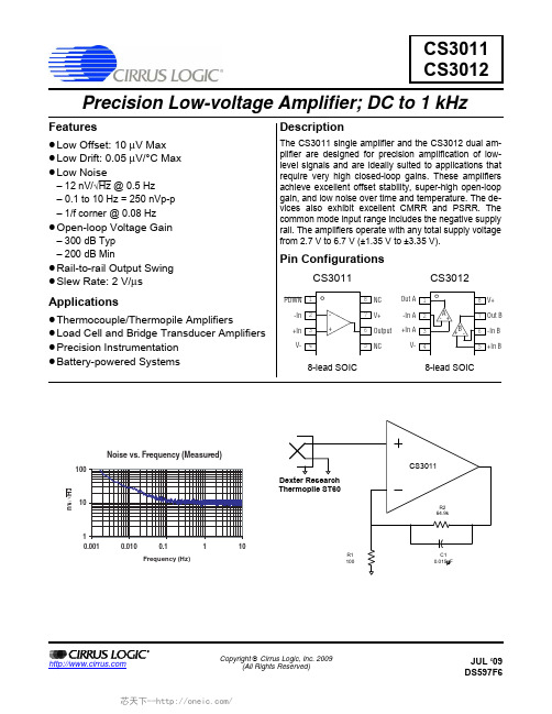
CS3011 CS3012
1. CHARACTERISTICS AND SPECIFICATIONS
ELECTRICAL CHARACTERISTICS
V+ = +5 V, V- = 0V, VCM = 2.5 V (Note 1) CS3011/CS3012 Parameter Input Offset Voltage Average Input Offset Drift Long Term Input Offset Voltage Stability Input Bias Current Input Offset Current Input Noise Voltage Density RS = 100 Ω, f0 = 1 Hz RS = 100 Ω, f0 = 1 kHz Input Noise Voltage Input Noise Current 0.1 to 10 Hz 0.1 to 10 Hz • (Note 4) (Note 5) • • • • Input Noise Current Density f0 = 1 Hz Input Common Mode Voltage Range Common Mode Rejection Ratio (dc) Power Supply Rejection Ratio Large Signal Voltage Gain RL = 2 kΩ to V+/2 Output Voltage Swing RL = 2 kΩ to V+/2 RL = 100 kΩ to V+/2 Slew Rate Overload Recovery Time Supply Current PWDN active (CS3011 Only) PWDN Threshold Start-up Time CS3011 CS3012 (Note 6) (Note 6) (Note 7) • • • • • RL = 2 k, 100 pF TA = 25º C TA = 25º C • • -0.1 115 120 200 +4.7 (Note 2) (Note 2) • • Min Typ ±0.01 (Note 3) ±50 ±100 12 12 250 100 1.9 120 136 300 +4.99 2 600 0.9 1.7 (V+)-1.25 1.4 2.4 15 12 ±1000 ±2000 pA pA
外加LNA 对零中频接收机性能之影响

Introduction在手机射频中,最常额外添加LNA的RF应用,应该莫过于讯号极为微弱的GPS,如下图[18] :然而随着手机射频越来越复杂,其他RF应用,也开始出现额外添加LNA的需求,如下图[9]。
故本文件将探讨外加LNA,对于接收机性能的影响。
Noise Figure所谓灵敏度,指的是在SNR能接受的情况下,其接收机能接收到的最小讯号[17],其公式如下:然而对于手机射频工程师而言,能着手改善灵敏度的,只有Noise Figure一项。
Noise Figure的定义如下[17] :理想上SNR当然是越大越好,最好是无限大(表示都没有噪声),但实际上不可能没有噪声,因此所谓Noise Figure,衡量的是当一个讯号进入一个系统时,其输出讯号的SNR下降多寡,亦即其噪声对系统的危害程度,示意图如下[17] :假设信号经过一组件,其SNR下降1 dB,那么我们可以说,该组件的Noise Figure 为1 dB。
而由下图可知,Noise Figure最小为零,亦即输出信号的SNR完全不变。
同时也由下图可知,信号经过任何组件,不管是有源还是无源,其SNR都只会变小,再怎样都不会变大,所以Noise Factor最小是1[14]。
因此,若信号经过越多组件,则SNR会下降越多[3]。
而不论是有源还是无源组件,其Noise Figure主要是来自其Insertion Loss。
当然,放大器在启动状态下,只有Gain,没有Insertion Loss,但即便如此,信号经过放大器,其SNR依旧只会下降,毕竟如前述所言,信号经过一组件,其SNR再怎样都不可能放大,因为Noise Figure最小为零,没有负的。
由上图可知,当信号经过一个LNA时,理论上SNR不变,因为信号与噪声会一起放大,且放大倍数一致。
但由于LNA会有自身的Additive Noise[3],提升了信号的Noise Floor,故输出信号的SNR会下降。
罗泽尔沙声监测仪(Roxar Sand Acoustic Monitor)产品数据表(RXPS-00
Product Data SheetRXPS-002251, Rev AFebruary 2019 Roxar Sand Acoustic MonitorNon-intrusive Sand MonitoringThe Roxar Sand Acoustic Monitor (SAM) is a non-intrusive sand monitoring system that identifies in real-time sand production in water, oil, gas or multiphase flow lines for onshore and offshore locations. It offers a cost effective tool for operators to optimize production by enabling the determination of maximum sand-free rates or maximum acceptable sand production rates.Roxar Sand Acoustic Monitor February 2019 Roxar Sand Acoustic MonitorDecreasing production costs are becoming more and more important as reservoirs are maturing. As a result, sand production needs to be closely measured and monitored in order to avoid serious damages. One consequence of increased sand production can be serious damage to production equipment, such as valves, chokes and pipe bends. If not controlled, high sand production can have a damaging impact on the integrity of the production system. Roxar SAM is valuable for ensuring production system integrity.The benefits of using Roxar SAM include:■Allows monitoring and prediction of erosion in process equipment in order to ensure safe production and reduced down time.■Enables optimized production through the determination of Maximum Sand Free Rate (MSFR) or Acceptable Sand Rates (ASR).■Allows for improved production processes in order to prevent pipelines or separators filling with sand.■Enables monitoring of sand screen integrity.The Roxar SAM is an acoustic type device and includes the following benefits:■Real time measurement of sand production in any water, oil, gas, or multiple flow line for onshore and offshore locations.■Quantification of sand accumulating in the system by calculating grams per second passing through the pipeline. This supports Acceptable Sand Rate (ASR), with on-site sand calibration measured against actual conditions in grams per second.■Ability to detect sand noise without calibration.■No mechanical moving parts, resulting in low maintenance.■Compact and low weight device.■Non-intrusive design benefits include:—No wetted parts—No pipe pressure drop—Easy to install—No shutdown required for installation—Easy to retrofit for existing installationsBuilding Blocks behind the Roxar SAMThe Roxar SAM design consists of several parts:■ A monitor consisting of a transducer and housing damped on to the pipe.■The basic safe area electronics consisting of a Calculation & Interface Unit (CIU) and a safety barrier.A.Flowline Monitor B.Safety Barrier C.Hazard D.Safe E.Power Supply (PSU) (optional)F.Calculation & Interface Unit (CIU)G.Service Bus RS232H.PC with service software (optional)I.Modbus RTU/RS485J.Volt Free Contact K.Hazardous Area L.Safe AreaFebruary 2019Roxar Sand Acoustic MonitorRoxar SAM working principleRoxar SAM is a non-intrusive device that utilizes the acoustic noise generated by the sand particles to derive a sand production measurement. It utilizes the fact that the sand, while transported with the flow, impacts the pipe wall due to inertia in pipe bends and creates noise. This noise is then processed and used to identify and calculate real-time sand production in any water, oil, gas or multiple pipeline flows.Figure 1: Pipe Bend and Process Flow with Digital Output (Mean Value/One Second)A.Sand-Generated Noise (Impact Center Point)B.Spring-Loaded Microphone C.Impacting Particles D.FlowThe sensor picks up noise that propagates in the pipe wall and converts it to a digital signal that is transmitted on the sensor signal and built-in algorithms. Detector readings are stored for up to 90 days in an internal flash drive based on 10 second average intervals.Roxar Sand Acoustic Monitor February 2019Figure 2: Piping installation GuidelinesA.Noise Amplitude %B.FrequencyC.Flow-generated NoiseD.Sand-generated NoiseE.Microphone FilterFebruary 2019Roxar Sand Acoustic MonitorRoxar Sand Acoustic Monitor February 2019 Technical specificationsInstallation requirementsThe detector unit is non-intrusive and can be installed in production pipe work of any diameter between 2” and 48”. To facilitate inspection, the Ex classification marking must be visible after installation.The figures below shows the assembly and envelope for the different versions available, Standard Temperature (ST) and High Temperature (HT) of a Roxar acoustic sensor. Dependent on specific models of acoustic sensors (PDS or SAM), some special installation requirements may apply. General Arrangement (GA) drawings for the different models and versions can be provided upon request. Contact your Emerson sales representatives for inquiries.Piping, ST, and HT installation guidelinesThe piping arrangement upstream of the of the detector/monitor depends on the model; see the detailed description for specific requirements.Figure 3: Piping installation GuidelinesA.Piping B.Cable (one twisted pair)C.Cable gland D.Mounting strap (AISI 316)February 2019Roxar Sand Acoustic MonitorFigure 4: ST Installation Guidelines A.Detector housing (AISI 316)B.Mounting socketC.Fastening arrangement (AISI 316)Figure 5: HT Installation GuidelinesA.Fastening arrangement (AISI 316)B.Mounting socketC.HT Detector housing (AISI 316)Roxar Sand Acoustic Monitor February 2019In order to achieve best sensitivity, the Roxar SAM should be installed downstream from and as close as possible to a 90° bend and not farther away than 75 cm. This is because of the need for the pipe geometry particle inertia work to increase the concentration and force of the particle impact, and thereby the sand response, allowing for high quality measurements. Care should be taken to avoid installation near known sources of unwanted noise, for example, choke valves or cyclonic de-sanding equipment. Excessive levels of unwanted noise may compromise the measurement principle.Figure 6: SAM Installation Near 90° BendInstallation considerationsFigure 7: Installation Use GuidelinesA.Green – Safe useB.Yellow – Safe use, but not recommended (risk for non-safety-critical sensor damage)C.Red – Unsafe use (outside certified temperature envelope)D.Ambient temperature: The temperature of air or other media in a designated area surround the equipment.E.Surface temperature of the pipe on which the equipment is mounted.February 2019Roxar Sand Acoustic MonitorStandard Temperature (ST) versionFor the ST version, the only installation requirement is that there is a space between the detector housing and the pipe installation to allow the heat to dissipate from the detector and the pipe. This space ensures the detector's temperature is kept as low as possible.Figure 8: ST version chartA.Green – Safe UseB.Yellow – Safe Use, But Not RecommendedC.Red – Unsafe UseRoxar Sand Acoustic Monitor February 2019High Temperature (HT) versionThe HT version must always be mounted horizontally on the pipe.The HT version also contains:■An extended waveguide 'noise' at the front end to retract the sensor electronics away from the hot pipe surface ■Vent holes in the detector housing to provide more efficient heat evacuationFigure 9: HT version chartA.Green – Safe UseB.Yellow – Safe Use, But Not RecommendedC.Red – Unsafe UseModel code numbering systemMode code structure for the Roxar Sand monitor - acousticA complete model code includes the ordering options.February 2019Roxar Sand Acoustic MonitorRoxar Sand Acoustic Monitor February 2019Product descriptionFunctional propertiesTable 1: Roxar SAM model code functional propertiesPipe sizeTable 2: Roxar SAM model code pipe sizeFebruary 2019Roxar Sand Acoustic MonitorMain material (sensor housing)Table 3: Roxar SAM model code sensor housingDetector approvalsRoxar SAM model code detector approvalsAll detector approvals are certified for Intrinsically Safe installations.Table 4: Roxar SAM model code pipe sizeField cable glandAll field cable glands have the following certification: Hawke 501/453/Universal Ex de.Table 5: Roxar SAM model code field cable gland(1)Not available with Factory option Z.Field cable size rangeCode 0 is only available with Field Cable Gland option G0 (no gland).Codes 1 through 4 are not available with Field Cable Gland option G0 (no gland).Roxar Sand Acoustic Monitor February 2019 Table 6: Roxar SAM model code field cable glandCommunication interfaceTable 7: Roxar SAM model code communication interface(1)Not available with Factory Option Z.Supply voltageTable 8: Roxar SAM model code supply voltage(1)Not available with Enclosure for Electronics in Hazardous Area option Z0, No Enclosure.BarrierRoxar SAM model code barrierField reset boxTable 9: Roxar SAM model code field reset boxFor future useTable 10: Roxar SAM model code future use Tag platesTable 11: Roxar SAM model code tag plates(1)Not available with factory option Z.Product specific optionsTable 12: Roxar SAM model code product specific options(1)Not available with factory Option Z.Factory optionsTable 13: Roxar SAM model code factory options February 2019Roxar Sand Acoustic MonitorRXPS-002251Rev. AFebruary 2019 RoxarHead Office Roxar products:+47 51 81 8800**********************CIS: +7 495 504 3405Europe: +47 51 81 8800North America: +1 281 879 2300Middle East: +971 4811 8100Asia Pacific: +60 3 5624 2888Australia: 1 300 55 3051Latin America:Portuguese: +55 15 3413 8888Spanish: + 52 55 5809 5000/Roxar©2019 Roxar AS. All rights reserved.The Emerson logo is a trademark and service mark of Emerson Electric Co. Roxar is a trademark ofRoxar ASA. All other marks are property of their respective owners.Roxar supplies this publication for informational purposes only. While every effort has been made toensure accuracy, this publication is not intended to make performance claims or processrecommendations. Roxar does not warrant, guarantee, or assume any legal liability for the accuracy,completeness, timeliness, reliability, or usefulness of any information, product, or process describedherein. All sales are governed by our terms and conditions, which are available on request. Wereserve the right to modify or improve the designs or specifications of our products at any timewithout notice. For actual product information and recommendations, please contact your localRoxar representative.Roxar products are protected by patents. See /en-us/automation/brands/roxar-home/roxar-patents for details.。
moto 链路预算

Uplink
Downlink coverage is smaller than Uplink coverage So you CAN NOT cell coverage .
USE MHA
to enhance
Cell coverage
-5-
Sardine Project
Uplink needs enlarged
TDF HCU DCF 4db DDF
7db Cable loss
-1db -3db (-1db)+(-3db)=(-1db)+(-3db)+(-3db)=-2db/30m (7/8 inch)
BTS max TX Power (Horizon DCS1800) 50w 47dbm BTS sensitivity 108.5dbm MS max TX Power (class 5) 1w 30dbm MS sensitivity -100dbm
Sardine Project
Link Budget
Cooperation
CMCC BeiJing Account SOS Team Prepared By: Yan Yi Chuan
Sardine Project
LINK BUDGET 含义 LINK BUDGET 计算 GSM1800 LINK BUDGET 计算 GSM900 LINK BUDGET 计算
- 16 -
Fading margin Body loss
-6db -3db
Sardine Project
Config A --- 0 Stage
Linkbudget For Motorola HorizonMacro
Frequency: 1710MHz - 1880MHz With mast head amplifier
Noise Figure Measurement Using Mixed-Signal BIST
Noise Figure Measurement Using Mixed-Signal BISTJie Qin, Charles Stroud, and Foster DaiDept. of Electrical and Computer Engineering, 200 Broun HallAuburn University, Alabama 36849-5201, USAAbstract—A Built-In Self-Test (BIST) approach for functionality measurements, including noise figure (NF), linearity and frequency response of analog circuitry in mixed-signal systems, is presented. The BIST circuitry consists of a direct digital synthesizer (DDS) based test pattern generator (TPG) and a multiplier/accumulator based output response analyzer (ORA). The BIST approach has been implemented in hardware and used for actual NF measurements for comparison with measurements from external test equipment.I.I NTRODUCTIONMixed-signal Built-In Self-Test (BIST) is now in more demand than ever. Analog functionality tests based on the traditional methodology of manual testing costs much more money and time due to the ever-increasing operational frequency and complexity of modern mixed-signal integrated circuits (ICs). For example, RFIC test cost can be as high as 50% of the total cost, depending on the complexity of the functionality to be tested [1]. The operational frequency and complexity of modern mixed-signal ICs make it difficult to perform tests on these ICs. With a rapidly increasing level of integration, the number of input/output (IO) pins does not increase accordingly such that observability of internal components is lower compared with traditional ICs [2]. Therefore, it becomes more attractive to automate the analog testing process with low-cost, built-in test circuitry.In order to perform a suite of analog functionality tests in a BIST environment, such as linearity, frequency response, and noise figure (NF) measurements, the frequency spectrum of the signal coming from the device under test (DUT) needs to be measured and analyzed by an output response analyzer (ORA) included in the BIST circuitry [3]. A few techniques have been proposed to perform on-chip frequency-domain testing of mixed-signal circuits in [4]–[7]. However, most of these approaches focus only on one or two simple parameter tests such as cut-off frequency of a filter and cannot perform complete analog tests such as frequency response, linearity, noise measurements [1].A new mixed-signal BIST approach has been proposed based on direct digital synthesizer (DDS) based test pattern generator (TPG) and multiplier/accumulator (MAC) based ORA. Because the signal is in digital form, it is easy to include different modulation capabilities in the DDS. Therefore, many analog functional tests, such as magnitude and phase response in the frequency domain, 3rd order intercept point (IP3) and noise figure (NF) can be performed in such an architecture [1]. Some experimental results for IP3 and frequency response (both phase and gain) using this BIST architecture have been presented in [1] to demonstrate the feasibility and accuracy of the BIST approach.In this paper, we show how the proposed BIST approach can be extended from the current suite of functional measurements to include NF measurements of the analog circuitry in a mixed-signal IC or system. The paper is organized as follows. An overview of the BIST approach is given in Section II. Next, the theoretical background of NF measurement and how the measurement is conducted in our BIST architecture are presented in Section III. Some experimental results of actual hardware NF measurements are given in Section IV. Finally, we summarize the paper in Section V with some concluding remarks.II.O VERVIEW OF BIST A PPROACHThe mixed-signal BIST architecture, illustrated in Figure 1, includes a DDS-based TPG, a MAC-based ORA, and a test controller [1]. The test scheme utilizes the existing digital-to-analog converters (DACs) and analog-to-digital converters (ADCs) typically associated with most mixed-signal architectures to minimize the hardware added for BIST. The only test circuitry added to the analog domain is loopback capabilities needed to facilitate return paths for test signals to the ORA. The number and location of loopback capabilities determines the accuracy and resolution of tests and measurements associated with a given analog function.The DDS-based TPG consists of three numerically controlled oscillators (NCOs) and utilizes an existing DAC from the mixed-signal system to complete the DDS. Figure 2 shows a more detailed view of an NCO used in the TPG. The phase accumulator is used to generate the phase word based on the frequency word f and initial phase word θ. A look-up table is utilized to convert the truncated phase word sequence to a digital sine wave sequence. The output sine wave frequency is determined as'2clknf ff⋅=, (1) where nis the word width of the phase accumulator.Figure 1. General model of BIST architectureFigure 2. NCO used in TPG The ORA consists of an N ×N -bit multiplier and an M -bit accumulator. In the design of the ORA, N is the number of bits from the DDS and ADC and M is chosen such that K <2M , where K is the length of the BIST sequence in clock cycles. While performing frequency response, linearity and NF measurements, f 1(nT clk ) and f 2(nT clk) (refer to Figure 1) are set to cos(ωnT clk ) and sin(ωnT clk ), respectively. As a result, the DC 1 and DC 2 accumulator values can be described as 1DC ()cos()clk clk nf nT nT ω=⋅∑,(2) 2DC ()sin()clk clk nf nT nT ω=⋅∑.(3) Reference [3] presents three approaches to calculate the amplitude response A(ω) and phase response ∆φ(ω) using DC 1 and DC 2 and points out that the most preferable approach for NF, linearity and frequency response measurements is based on (4) and (5) as follows 2221)(DC DC A +=ω. (4) 121()()()DC tgDC ωφωω−∆=−, (5) In order to achieve accurate results for analog functional measurements, not only must the DUT’s phase response be considered and measured as in Equation (5), but also the phase delay caused by the BIST circuitry itself (including the DAC and ADC) needs to be measured for calibration of measurements [1][3]. This is done by controlling MUX3 in Figure 1 to select the signal path without the DUT to measure and calibrate for phase delay in the BIST circuitry. III. N OISE F IGURE M EASUREMENTNoise figure (NF) measurement is an important analogfunctionality test along with the IP3 and frequency responsemeasurements. Noise introduced by analog circuitry includes thermal noise, shot noise, flicker noise, etc. [8]. The noisefrom these sources will be mixed together with the signal ofinterest. The more noise that is introduced by circuit components, the more difficult it is to extract the signal ofinterest. Therefore, the noise is a critical issue to anyelectrical system’s performance. If the noise introduced bycritical components, like low noise amplifiers (LNAs), can be measured in the system, it will be much easier for IC and system manufacturers to test and diagnose potential problems related to noise in mixed-signal systems. Therefore, it is important to include NF measurements in the BIST approach. There are two important parameters widely used to characterize the system noise. One is the signal-to-noise ratio (SNR), which is defined asSignal Power SNR Noise Power in Interested Bandwidth = (6) Alternatively, the noise added in a circuit can be characterized by the noise figure (NF), which is defined as in outSNR NF SNR =, (7) where SNR in and SNR out are the SNRs measured at the input and output of the circuit, respectively [8]. The noise introduced by a DUT can be mathematicallymodeled as illustrated in Figure 3 where y out (t) is the response of the DUT’s ideal model to the input signal y in (t), while y n (t)represents the noise generated by the DUT. Without loss of generality, y n (t) is usually assumed to be a white Gaussianadditive noise. The measurement of noise is computed in the frequency domain instead of the time domain mainly due to the following two factors. First, it is very hard to estimate y n (t)’s power from the time domain and, second, even if we can find a way to determine y n (t)’s power, it is still meaningless because we only care about the noise over the bandwidth of interest, which is usually much smaller thany n (t)’s real power [2][8]. Phase Accumulator)Figure 3. Noise introduced by DUTAccording to the periodogram method [9], the noise’spower spectrum density (PSD) in sampled discrete format can be expressed as221'01()()()N j nk L out clk out clk n clk S k y nT y nT e Nf π−=⎡⎤=−⎣⎦∑(8) Usually, Equation (8) can be computed through the FFT algorithm. However, there is a large area penalty and power consumption associated with an on-chip (or in-system) FFT processor [3][7]. To perform the NF measurement in our BIST approach (refer to Figure 1), NCO1 in the TPG of the BIST circuitry generates a sine wave sin (ω1t ) to stimulate the DUT. At the same time, an in-phase tone and an out-of-phase tone at frequency ω2 are produced by NCO2 and NCO3, respectively, and fed into the ORA. In this case, frequency words to NCO2 and NCO3 were be the same, f 2 = f 3, while θ2 and θ3 are used to control the in-phase and out-of-phase tones at frequency ω2. By sweeping ω2 over the frequency band of interest, the ORA can then obtain y’out (t)’s spectrum information as illustrated in Figure 4. Since the signal of interest only appears at frequency f 1, the spectrum of the noise Y n (f) can be easily obtained from the samples at all other frequencies. Then the noise’s PSD and SNR can be measured based on Equations (8) and (6), respectively. The test controller is capable of bypassing the DUT through MUX3 (see Figure 1) such that input and output SNRs of the DUT can be measured. From these two SNRs, the NF of the DUTcan be determined using Equation (7).Figure 4. SNR measurement using BISTIV. E XPERIMENTAL R ESULTSIn order to prove the effectiveness and feasibility of theproposed BIST architecture for NF measurements of analog circuitry in addition to linearity and frequency response measurements, we implemented the BIST architecture shownin Figure 1 in hardware. The digital portion of the BISTcircuitry was implemented in a Xilinx Spartan XC2S50 FieldProgrammable Gate Array (FPGA) on an XSA50 printed circuit board (PCB). A DAC (AD9752AR by AnalogDevices) with low-pass filter and an 8-bit ADC (AD9225AR by Analog Devices) were implemented on another PCB. An op-amp built on a separate board served as the DUT for the NF measurement.A. NF Measurement using External Test EquipmentIn order to verify the accuracy of the BIST-based NF measurement, a reference NF measurement was conducted using external test equipment, including an Agilent 33250A waveform generator and an Agilent 8563EC spectrumanalyzer. The DUT was driven by the waveform generator and the DUT’s input and output were analyzed by the spectrum analyzer with a resolution bandwidth (RBW) of 100Hz. The spectrum of the DUT’s input and output were captured and are shown in Figures 5 and 6, respectively. It should be noted that the maximum signal level in Figure 5coincides with the top of the plot.Figure 5. DUT input spectrum analyzer SNFR measurement of90 dBc/HzFigure 6. DUT output spectrum analyzer SNFR measurement of 76 dBc/Hz It is known from [10] that the SNR can be read from the spectrum analyzer as follows1010log (2)s f SNR SNFR RBW ⎛⎞=−⎜⎟•⎝⎠, (9)where SNFR is the signal-to-noise floor ratio displayed directly on the spectrum analyzer. The SNFR in and SNFR out at the DUT’s input and output as read from these two figures are 90 dBc/Hz and 76 dBc/Hz, respectively. The DUT’s NF can be now be calculated as follows1907614 in outNF SNFR SNFR dB=−=−=(10) B.NF Measurement using BIST circuitryThe BIST-based NF measurement was conducted and the actual input and output spectrums obtained from the BIST circuitry are shown in Figures 7 and 8, respectively. From these two figures, the SNFR in and SNFR out of the DUT are read as 60 dBc/Hz and 45 dBc/Hz, respectively, using the noise floor indicated in the figures. The DUT’s NF can be calculated in the same way as Equation (10) and the result is2604515 in outNF SNFR SNFR dB=−=−=(11)Figure 7. DUT input BIST-based SNFR measurement of 60dBc/HzFigure 8. DUT output BIST-based SNFR measurement of 45dBc/HzComparing the NF1from Equation (10) using external test equipment and NF2 from Equation (11) using the BIST circuitry, we find that there is only 1 dB difference between the two measurements. This illustrates the feasibility and accuracy of the BIST approach for NF measurements. One possible reason for the 1dB difference is the choice of noise floor for the measurement indicated in the figures. Another possible reason is switching noise produced by the FPGA that is not observed by the external test equipment.V.C ONCLUSIONSA BIST approach for analog circuit functional tests, including NF measurements as well as linearity and frequency response, in mixed-signal systems was presented. The experimental results show the feasibility and accuracy of the BIST architecture for on-chip NF measurements. The BIST architecture has been implemented in Verilog and parameterized for specification of the desired size of the DDS-based TPG and MAC-based ORA based on the sizes of the DAC and ADC targeted for the mixed-signal system. The BIST implementation is efficient in terms of area and easily fits into the smallest FPGAs on the market. As a result, it can be easily incorporated in any mixed-signal system design. This facilitates permanent residence of the BIST circuitry in system applications with access to the DAC/ADC pair for on-chip analog functional test and measurement. It should be noted that the BIST architecture shown in Figure 1 includes all of the circuitry, features, and capabilities needed for linearity and frequency response (both gain and phase) measurements as well as NF measurement. Furthermore, the NF measurement requires only a subset of the circuitry shown in Figure 1 and does not impose any additional circuitry on the existing BIST architecture.R EFERENCES[1] F. Dai, C. Stroud, and D. Yang, “Automatic Linearityand Frequency Response Tests with Built-in Pattern Generator and Analyzer,” IEEE Trans. on VLSI Systems.,vol. 14, no. 6, pp. 561-572, 2006.[2]M. Bushnell and V. Agrawal, Essentials of ElectrnonicTesting for Digital, Memory and Mixed-Signal VLSI Circuits, Springer, 2006.[3]J. Qin, C. Stroud, and F. Dai, “Phase Delay Measurementand Calibration in Built-In Analog Functional Test,” to be published in Proc. IEEE Southeastern Symp. on System Theory, March 2007.[4] C.-Y. Chao, H.-J. Lin, and L. Milor, “Optimal Testing ofVLSI Analog Circuits,” IEEE Trans. on Computer-Aided Design, vol. 16, no. 1, pp. 58-76, 1997.[5]M. Toner and G. Roberts, “A BIST Technique for aFrequency Response and Intermodulation Distortion Test of a Sigma-Delta ADC,” Proc. IEEE VLSI Test Symp.,pp. 60-65, 1994.[6] B. Provost and E. Sanchez-Sinencio, “On-chip RampGenerators for Mixed-Signal BIST and ADC Self-Test,”IEEE J. Solid-State Circuits, vol. 38, pp. 263-273, 2003. [7]J. Emmert, J. Cheatham, B. Jagannathan, and S.Umarani, “An FFT Approximation Technique Suitable for On-Chip Generation and Analysis of Sinusoidal Signals”, Proc. IEEE International Symp. on Defect and Fault Tolerance in VLSI Systems, pp. 361-367, 2003.[8] B. Razavi, RF Microelectronics, Prentice-Hall, 1997.[9] A. Oppenheim and R. Schafer, Discrete-Time SingalProcessing, Prentice-Hall, 1989.[10]W. Kester, Editor, Analog-Digital Conversion, AnalogDevices Inc, 2004.Noise floor Noise floor。
噪声系数测量的三种方法
Maxim > App Notes > BASESTATIONS / WIRELESS INFRASTRUCTURE WIRELESS, RF, AND CABLEKeywords: rf, rfic, wireless, noisefigure measurement, gain, meter, y factor, rf ics, rfics Nov 21, 2003 APPLICATION NOTE 2875Three Methods of Noise Figure MeasurementAbstract: Three different methods to measure noise figure are presented: Gain method, Y-factor method, and the Noise Figure Meter method. The three approaches are compared in a table.IntroductionIn wireless communication systems, the "Noise Figure (NF)," or the related "Noise Factor (F)," defines the noise performance and contributes to the receiver sensitivity. This application note describes this important parameter and details ways to measure it.Noise Figure and Noise FactorNoise Figure (NF) is sometimes referred to as Noise Factor (F). The relationship is simply:NF = 10 * log10 (F)DefinitionNoise Figure (Noise Factor) contains the important information about the noise performance of a RF system. The basic definition is:From this definition, many other popular equations of the Noise Figure (Noise Factor) can be derived.Below is a table of typical RF system Noise Figures:Category MAXIM Products Noise Figure*Applications Operating Frequency System GainLNA MAX26400.9dB Cellular, ISM400MHz ~ 1500MHz15.1dBLNA MAX2645HG: 2.3dB WLL 3.4GHz ~ 3.8GHz HG: 14.4dB LG: 15.5dB WLL 3.4GHz ~ 3.8GHz LG: -9.7dBMixer MAX268413.6dB LMDS, WLL 3.4GHz ~ 3.8GHz1dBMixer MAX998212dB Cellular, GSM825MHz ~ 915MHz 2.0dBReceiver System MAX2700 3.5dB ~ 19dB PCS, WLL 1.8GHz ~ 2.5GHz< 80dB* HG = High Gain Mode, LG = Low Gain ModeMeasurement methods vary for different applications. As shown in the table above, some applications have high gain and low noise figure (Low Noise Amplifiers under HG mode), some have low gain and high noise figure (mixers and LNAs under LG mode), some have very high gain and wide range of noise figure (receiver systems). Measurement methods have to be chosen carefully. In this article, a Noise Figure Meter as well as two other popular methods - "gain method" and "Y factor method" - will be discussed.Using a Noise Figure MeterNoise Figure Meter/Analyzer is employed as shown in Figure 1.Figure 1.The noise figure meter, such as Agilent N8973A Noise Figure Analyzer, generates a 28VDC pulse signal to drive a noise source (HP346A/B), which generates noise to drive the device under test (DUT). The output of the DUT is then measured by the noise figure analyzer. Since the input noise and Signal-to-Noise ratio of the noise source is known to the analyzer, the noise figure of the DUT can be calculated internally and displayed. For certain applications (mixers and receivers), a LO signal might be needed, as shown in Figure 1. Also, certain parameters need to be set up in the Noise Figure Meter before the measurement, such as frequency range, application (Amplifier/Mixer), etc.Using a noise figure meter is the most straightforward way to measure noise figure. In most cases it is also the most accurate. An engineer can measure the noise figure over a certain frequency range, and the analyzer can display the system gain together with the noise figure to help the measurement. A noise figure meter also has limitations. The analyzers have certain frequency limits. For example, the Agilent N8973A works from 10MHz to 3GHz. Also, when measuring high noise figures, e.g., noise figure exceeding 10dB, the result can be very inaccurate. This method requires very expensive equipment.Gain MethodAs mentioned above, there are other methods to measure noise figure besides directly using a noise figure meter. These methods involve more measurements as well as calculations, but under certain conditions, they turn out to be more convenient and more accurate. One popular method is called "Gain Method", which is based on the noise factor definition given earlier:In this definition, "Noise" is due to two effects. One is the interference that comes to the input of a RF system in the form of signals that differ from the desired one. The second is due to the random fluctuation of carriers in the RF system (LNA, mixer, receiver, etc). The second effect is a result of Brownian motion, It applies in thermal equilibrium to any electronic device, and the available noise power from the device is:P NA = kT∆F,Where k = Boltzmann's Constant (1.38 * 10-23 Joules/∆K),T = Temperature in Kelvin,∆F = Noise Bandwidth (Hz).At room temperature (290∆K), the noise power density P NAD = -174dBm/Hz.Thus we have the following equation:NF = P NOUT - (-174dBm/Hz + 10 * log10(BW) + Gain)In the equation, P NOUT is the measured total output noise power. -174dBm/Hz is the noise density of 290°K ambient noise. BW is the bandwidth of the frequency range of interest. Gain is the system gain. NF is the noise figure of the DUT. Everything in the equation is in log scale. To make the formula simpler, we can directly measure the output noise power density (in dBm/Hz), and the equation becomes:NF = P NOUTD + 174dBm/Hz - GainTo use the "Gain Method" to measure the noise figure, the gain of the DUT needs to be pre-determined. Then the input of the DUT is terminated with the characteristic impedance (50Ω for most RF applications, 75Ω for video/cable applications). Then the output noise power density is measured with a spectrum analyzer.The setup for Gain Method is shown in Figure 2.Figure 2.As an example, we measure the noise figure of the MAX2700. At a specified LNA gain setting and V AGC, the gain is measured to be 80dB. Then, set up the device as show above, and terminate the RF input with a 50Ωtermination. We read the output noise density to be -90dBm/Hz. To get a stable and accurate reading of the noise density, the optimum ratio of RBW (resolution bandwidth) and VBW (video bandwidth) is RBW/VBW = 0.3. Thus we can calculate the NF to be:-90dBm/Hz + 174dBm/Hz - 80dB = 4.0dB.The "Gain Method" can cover any frequency range, as long as the spectrum analyzer permits. The biggest limitation comes from the noise floor of the spectrum analyzer. As shown in the equations, when Noise Figure is low (sub 10dB), (P OUTD - Gain) is close to -170dBm/Hz. Normal LNA gain is about 20dB. In that case, we need to measure a noise power density of -150dBm/Hz, which is lower than the noise floor of most spectrum analyzers. In our example, the system gain is very high, thus most spectrum analyzers can accurately measure the noise figure. Similarly, if the Noise Figure of the DUT is very high (e.g., over 30dB), this method can also be very accurate.Y Factor MethodY Factor method is another popular way to measure Noise Figure. To use the Y factor method, an ENR (Excess Noise Ratio) source is needed. It is the same thing as the noise source we mentioned earlier in the "Noise Figure Meter" section. The setup is shown in the Figure 3:Figure 3.The ENR head usually requires a high DC voltage supply. For example, HP346A/B noise sources need 28VDC. Those ENR heads works are a very wide band (e.g.10MHz to 18GHz for the HP346A/B) and they have a standard noise figure parameter of their own at specified frequencies. An example table is given below. The noise figures at frequencies between those markers are extrapolated.Table 1. Example of ENR of Noise HeadsHP346A HP346BFrequency (Hz)NF (dB)NF (dB)1G 5.3915.052G 5.2815.013G 5.1114.864G 5.0714.825G 5.0714.81Turning the noise source on and off (by turning on and off the DC voltage), an engineer measures the change in the output noise power density with a spectrum analyzer. The formula to calculate noise figure is:In which ENR is the number given in the table above. It is normally listed on the ENR heads. Y is the difference between the output noise power density when the noise source is on and off.The equation comes from the following:An ENR noise head provides a noise source at two "noise temperatures": a hot T = TH (when a DC voltage is applied) and a cold T = 290°K. The definition of ENR of the noise head is:The excess noise is achieved by biasing a noisy diode. Now consider the ratio of power out from the amplifier (DUT) from applying the cold T = 290°K, followed by applying the hot T = T H as inputs:Y = G(Th + Tn)/G(290 + Tn) = (Th/290 + Tn/290)/(1 + Tn/290).This is the Y factor, from which this method gets its name.In terms of Noise figure, F = Tn/290+1, F is the noise factor (NF = 10 * log(F))Thus, Y = ENR/F+1. In this equation, everything is in linear regime, from this we can get the equation above.Again, let's use MAX2700 as an example of how to measure noise figure with the Y-factor method. The set up is show above in Figure 3. Connect a HP346A ENR noise head to the RF input. Connect a 28V DC supply voltage to the noise head. We can monitor the output noise density on a spectrum analyzer. By Turning off then turning on the DC power supply, the noise density increased from -90dBm/Hz to -87dBm/Hz. So Y = 3dB. Again to get a stable and accurate reading of the noise density, RBW/VBW is set to 0.3. From Table 1, at 2GHz, we get ENR = 5.28dB. Thus we can calculate the NF to be 5.3dB.SummaryIn this article, three methods to measure the noise figure of RF devices are discussed. They each have advantages and disadvantages and each is suitable for certain applications. Below is a summary table of the pros and cons. Theoretically, the measurement results of the same RF device should be identical, but due to limitations of RF equipment (availability, accuracy, frequency range, noise floor, etc), we have to carefully choose the best method to get the correct results.Suitable Applications Advantage DisadvantageNoise FigureMeter Super low NF Convenient, veryaccurate when measuringsuper low (0-2dB) NF.Expensive equipment, frequencyrange limitedGain Method Very high Gain or very highNF Easy setup, very accurateat measuring very highNF, suitable for anyfrequency rangeLimited by Spectrum Analyzernoise floor. Can't deal withsystems with low gain and lowNF.Y Factor Method Wide range of NF Can measure wide rangeof NF at any frequencyregardless of gainWhen measuring Very high NF,error could be large.Application Note 2875: /an2875More InformationFor technical support: /supportFor samples: /samplesOther questions and comments: /contactAutomatic UpdatesWould you like to be automatically notified when new application notes are published in your areas of interest? Sign up for EE-Mail.Related PartsMAX2640:QuickView-- Full (PDF) Data Sheet-- Free Samples MAX2641:QuickView-- Full (PDF) Data Sheet-- Free Samples MAX2642:QuickView-- Full (PDF) Data Sheet-- Free Samples MAX2643:QuickView-- Full (PDF) Data Sheet-- Free Samples MAX2645:QuickView-- Full (PDF) Data Sheet-- Free Samples MAX2648:QuickView-- Full (PDF) Data SheetMAX2649:QuickView-- Full (PDF) Data SheetMAX2654:QuickView-- Full (PDF) Data Sheet-- Free Samples MAX2655:QuickView-- Full (PDF) Data Sheet-- Free Samples MAX2656:QuickView-- Full (PDF) Data Sheet-- Free Samples MAX2684:QuickView-- Full (PDF) Data Sheet-- Free Samples MAX2700:QuickView-- Full (PDF) Data Sheet-- Free Samples MAX9982:QuickView-- Full (PDF) Data Sheet-- Free SamplesAN2875, AN 2875, APP2875, Appnote2875, Appnote 2875 Copyright © by Maxim Integrated ProductsAdditional legal notices: /legal。
现代数字信号处理仿真作业

第三章仿真作业3.17(1)代码clear;N=32;m=[-N+1:N-1];noise=(randn(1,N)+j*randn(1,N))/sqrt(2); f1=0.15;f2=0.17;f3=0.26;SNR1=30;SNR2=30;SNR3=27;A1=10^(SNR1/20);A2=10^(SNR2/20);A3=10^(SNR3/20);signal1=A1*exp(j*2*pi*f1*(0:N-1));signal2=A2*exp(j*2*pi*f2*(0:N-1));signal3=A3*exp(j*2*pi*f3*(0:N-1));un=signal1+signal2+signal3+noise;uk=fft(un,2*N);sk=(1/N) *abs(uk).^2;r0=ifft(sk);r1=[r0(N+2:2*N),r0(1:N)];r=xcorr(un,N-1,'biased');figuresubplot(2,2,1)stem(m,real(r1));xlabel('m');ylabel('FFT估计r1实部');subplot(2,2,2)stem(m,imag(r1));xlabel('m');ylabel('FFT估计r1虚部');subplot(2,2,3)stem(m,real(r));xlabel('m');ylabel('平均估计r实部');subplot(2,2,4)stem(m,imag(r));xlabel('m');ylabel('平均估计r虚部');仿真结果(2)代码 clear; N=256;noise=(randn(1,N)+j*randn(1,N))/sqrt(2); f1=0.15; f2=0.17; f3=0.26; SNR1=30; SNR2=30; SNR3=27;A1=10^(SNR1/20); A2=10^(SNR2/20); A3=10^(SNR3/20);signal1=A1*exp(j*2*pi*f1*(0:N-1)); signal2=A2*exp(j*2*pi*f2*(0:N-1)); signal3=A3*exp(j*2*pi*f3*(0:N-1)); un=signal1+signal2+signal3+noise;-40-2002040-200020004000mF F T 估计r 1实部-40-2002040-2000-1000010002000mF F T 估计r 1虚部-40-2002040-200020004000m平均估计r 实部-40-2002040-2000-1000010002000m平均估计r 虚部spr=fftshift((1/NF)*abs(fft(un,NF)).^2);f1=(0:length(spr)-1)*(1/(length(spr)-1))-0.5; M=64;r=xcorr(un,M,'biased');bt=fftshift(abs(fft(r,NF)));f2=(0:length(bt)-1)*(1/(length(bt)-1))-0.5; figuresubplot(1,2,1)plot(f1,10*log10(spr/max(spr))); xlabel('w/2pi'); 仿真结果(3) 代码clear; N=1000;fai1=rand(1,1)*2*pi; fai2=rand(1,1)*2*pi;noise=(randn(1,N)+j*randn(1,N))/sqrt(2);un=exp(j*0.5*pi*(0:N-1)+j*fai1)+exp(-j*0.3*pi*(0:N-1)+j*fai2)+noise; p=8;cx=xcorr(un,p,'biased'); rxx=cx(p+1:2*p)'; R=toeplitz(rxx); [u,s]=eig(R);w/2piw/2piww=[-128:128]/128*pi;e=exp(-j*ww'*[0:p-1])%k行m列ev=e*u(:,1:p-2);pw=1./real(diag(ev*ev'));plot(ww/(2*pi),10*log10(pw)/max(pw));仿真结果-4-0.5-0.4-0.3-0.2-0.100.10.20.30.40.53.20(1)代码clear;N=1000;fai1=rand(1,1)*2*pi;fai2=rand(1,1)*2*pi;noise=(randn(1,N)+j*randn(1,N))/sqrt(2);un=exp(j*0.5*pi*(0:N-1)+j*fai1)+exp(-j*0.3*pi*(0:N-1)+j*fai2)+noise;p=8;cx=xcorr(un,p,'biased');rxx=cx(p+1:2*p)';R=toeplitz(rxx);[u,s]=eig(R);nw=128;ww=[-128:128]/128*pi;e=exp(-j*ww'*[0:p-1])%k行m列ev=e*u(:,1:p-2);pw=1./real(diag(ev*ev'));plot(ww/(2*pi),10*log10(pw)/max(pw));仿真结果距离单位圆最近的两个解为-0.2363-0.9717i和0.3747+0.9271i,对应的归一化频率为0.1889和-0.2880(2)代码clear;N=1000;fai1=rand(1,1)*2*pi;fai2=rand(1,1)*2*pi;noise=(randn(1,N)+j*randn(1,N))/sqrt(2);un=exp(j*0.5*pi*(0:N-1)+j*fai1)+exp(-j*0.3*pi*(0:N-1)+j*fai2)+noise; p=8;cx=xcorr(un,p,'biased');rxx=cx(p+1:2*p)';R=toeplitz(rxx);[u,s]=eig(R);nw=128;ww=[-128:128]/128*pi;e=exp(-j*ww'*[0:p-1])%k行m列ev=e*u(:,1:p-2);pw=1./real(diag(ev*ev'));plot(ww/(2*pi),10*log10(pw)/max(pw));仿真结果3.21-2-1123456-3clear;N=1000;fai1=rand(1,1)*2*pi;fai2=rand(1,1)*2*pi;noise=(randn(1,N)+j*randn(1,N))/sqrt(2);un=exp(j*0.5*pi*(0:N-1)+j*fai1)+exp(-j*0.3*pi*(0:N-1)+j*fai2)+noise; p=8;for k=1:N-pxs(:,k)=un(k+p-1:-1:k)';endrxx=xs(:,1:end-1)*xs(:,1:end-1)'/(N-p-1);rxy=xs(:,1:end-1)*xs(:,2:end)'/(N-p-1);[u,e]=svd(rxx);ev=diag(e);emin=ev(end);z=[zeros(p-1,1),eye(p-1);0,zeros(1,p-1)];cxx=rxx-emin*eye(p);cxy=rxy-emin*z;[U,E]=eig(cxx,cxy);Z=diag(E);ph=angle(Z)/(2*pi);err=abs(abs(Z)-1);仿真结果最接近单位圆的两个解分别为0.5867+0.8097i和0.0349-0.9984i,对应的归一化频率为0.1502和-0.2444。
- 1、下载文档前请自行甄别文档内容的完整性,平台不提供额外的编辑、内容补充、找答案等附加服务。
- 2、"仅部分预览"的文档,不可在线预览部分如存在完整性等问题,可反馈申请退款(可完整预览的文档不适用该条件!)。
- 3、如文档侵犯您的权益,请联系客服反馈,我们会尽快为您处理(人工客服工作时间:9:00-18:30)。
16
Thanks !!
17
2. The noise figure is simply the noise factor expressed in decibels (dB).
4
DEFINITION
5
Defini) * N (out) N (out) Na GN (in) S / N (out) GS (in) * N (in) GN (in) GN (in)
RX Noise Figure STUDY
1
OUTLINE
Block diagram Noise figure
Definition NF calculate Noise source
2
Block diagram
Antenna A
Block diagram of 2 branch of RX chain
Na GN (in) ) GN (in) 10 log10 ( Na GN (in)) 10 log10 (GN (in)) NF 10 log10 (
6
Methods of Noise Figure Measuring
Y factor measuring method
Gain measurement method Two times the power method Direct measuring method
7
Y factor measuring method
•
目前实际工程和研究中最常用的噪声系数测量方法是Y 因子法,各 种 噪声系数分析仪也都普遍使用Y 因子法进行噪声系数测量。噪声源 是Y 因子法测量必不可少的设备, 噪声源是能产生两种不同噪声功率 的噪声发生器。 通常需DC 脉冲电源驱动电压, 如常用的HP346A/ B/ C 系列噪声源需 要 +28VDC, 当+28V 供电时, 相当于噪声源开, 称为热态, 此时输出大的 噪声功率; 电源关闭时, 相当于噪声源关,称为冷态, 此时输出常温下的 噪声功率。 •Y因子方法 •–通过测量噪声源在两个不同等效输入噪声温度情况下,被测网络的 输出噪声功率来确定低噪声电路的噪声系数的方法被称为Y因子方法
13
Gain measurement method
14
Noise figure_ Test setup
› Test setup: Noise figure test setup with noise source for RX A/B
I/O to Data 1/2
duplexer
15
噪声系数测试的误差源
PAB TRXB
LNA1 T/R SW Limiter
TX A
FU
RF filter LNA2 optional
RF VGA
I
LNA1 T/R SW Limiter
RF VGA
I
TRXB
RF AGC
RF mixer
RF filter
00 180
IF ASIC
IF filter IF VGA IF AGC
8
Noise source
产生噪声的装置,是指能够获得高频噪声的部件 常用的噪声源组成: 雪崩二极管 匹配网络
注:商用噪声源用ENR来描述性能指标
9
Noise figure calculation
超噪比ENR(Excess Noise Ratio)
噪声源超过标准噪声温度T0热噪声的倍数,即
IF filter
ADC
16 ADC
I I
2bit 6dB step attenuator
UL digital
00 180
16 ADC
6bit step attenuator
1bit step attenuator
ADC clock
RF LO
3
Noise figure_ Definition
• Definition: • Noise factor (F) and Noise figure (NF) 1. The noise factor s defined as the ratio of input SNR to output SNR.
T T0 ENR T0
T T0 ENR(dB) 10lg T0
T为噪声源开时的噪声温度,T0为标准噪声温度290K
10
Noise figure calculation
11
Noise figure calculation
12
Noise figure calculation