PB5350数据
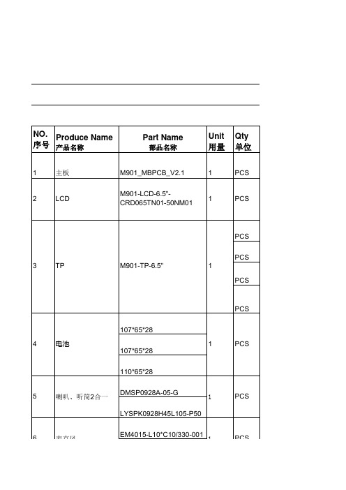
天炬科技M901BOM表
抗干扰焊线式0415,加胶套@4.6X2.2,线长10.0mm 0.35
莱音 卓越声
1020焊线式.扁平式,底部带3m胶, 线长50mm (匹配时代精创G65外壳) (匹配时代精创G65外壳) 前30w后30w GC0329+GC0328(BTB型) 前30w后200w GC0329+GC2035(BTB型) 前30w后30w GC0329+GC0328(BTB型) 前30w后200w GC0329+GC2035(BTB型) 光线传感器+距离传感器(选配) PC+ABS高光抛光 PC+ABS 素材 玻璃材质加硬处理 电镀+丝印 ABS 素材高光效果 ABS素材晒纹 不锈铁(M1.4x3.5mm),机丝 TPU材料 单面带背胶 3M 9448 9*8,单面带背胶
PCS 107*65*28 4 电池 107*65*28 110*65*28 DMSP0928A-05-G LYSPK0928H45L105-P50 EM4015-L10*C10/330-001 1 PCS
5
喇叭、听筒2合一
1
PCS
6
麦克风
1
PCS
6
麦克风 LYMIC4618CRL10 ZYS 1020-L50 WY-1020-50-A
陈桃林13724338077区超立1359来自304983 带USB的充电头
3M 9448,详见图纸 高温胶,详见图纸
1套 5
21 22 23 24 25 26
高温胶2 高温胶3 高温胶4 导电布1 导电布2 听筒网
高温胶,详见图纸 高温胶,详见图纸 高温胶,详见图纸 导电布,详见图纸 导电布,详见图纸 无坊布,详见图纸
1 1 2 1 1 1
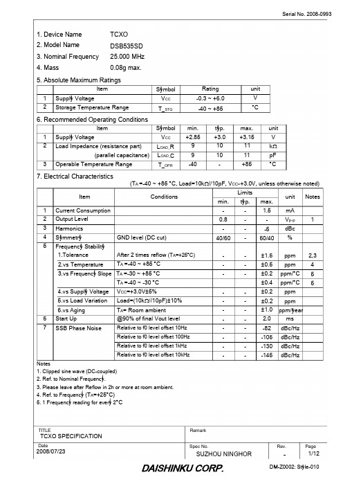
KDS TCXO 5032 DSB535SD 25MHZ规格书
9. Measurement Circuit
1000pF
mA +
Power Supply #8 #5 Output
T.P.
10000pF
V
Vcc
TCXO
GND #1 GND #4
-
Load_R
Load C
Load_R=10kΩ Load_C=10pF (Include Jig stray capacitance)
TITLE Date
Requirements
df/f=<±1.0ppm
2
Vibration
df/f=<±0.5ppm
df/f=<±0.5ppm
3
Shock
4
PCB bend strength
df/f=<±0.5ppm No visible damage.
5
Adherence nature
df/f=<±0.5ppm No visible damage.
(1) (2)
KDS
#1index
#2 #3 #4 #5 #6 #7 #8
(3)
Marking (1) Frequency 25000 (kHz, 5digits) (2) Model code B535SD (3) EIA Date code Year (1digit) + Week (2digits) e.g. 2008/1/1 801 unit: mm Dimensional Tolerance: ±0.15
-
1/12
DAISHINKU CORP.
DM-Z0002: Style-010
8. Outline, Pin Connections
DC DC模块电源IB05_S-W75R3系列商品说明书
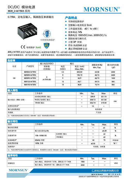
选型表认证产品型号输入电压(VDC)输出满载效率(%)Min./Typ.最大容性负载(µF)标称值(范围值)电压(VDC)电流(mA)Max./Min.CEIB0503S-W75R35(4.75-5.25)3.3200/2064/682400IB0505S-W75R35150/1568/722400IB0509S-W75R3983/968/721000IB0512S-W75R31262/769/73560IB0515S-W75R31550/570/74560输入特性项目工作条件Min.Typ.Max.单位输入电流(满载/空载)3.3VDC/5VDC 输出--209/5221/10mA9VDC/12VDC 输出--208/12221/2015VDC 输出--202/18215/30反射纹波电流*--15--输入滤波器类型电容滤波热插拔不支持注:*反射纹波电流测试方法详见《DC-DC (定压)模块电源应用指南》。
输出特性项目工作条件Min.Typ.Max.单位输出电压精度----±3%线性调节率输入电压变化±1%----±0.25%负载调节率10%-100%负载 3.3VDC 输出----±3%其他输出----±2纹波&噪声*20MHz 带宽--3075mVp-p 温度漂移系数100%负载--±0.02--%/℃短路保护可持续,自恢复注:*纹波和噪声的测试方法采用平行线测试法,具体操作方法参见《DC-DC (定压)模块电源应用指南》。
通用特性项目工作条件Min.Typ.Max.单位绝缘电压输入-输出,测试时间1分钟,漏电流小于1mA 1500----VDC输入-输出,测试时间1秒,漏电流小于1mA3000----0.75W ,定电压输入,隔离稳压单路输出专利保护RoHS产品特点●可持续短路保护●空载输入电流低至5mA ●工作温度范围:-40℃to +85℃●效率高达74%●隔离电压1500VDC/min,3000VDC/1s ●国际标准引脚方式●小型SIP 封装●符合UL62368认证●通过EN62368认证IB05_S-W75R3系列产品是专门针对板上电源系统中需要产生一组与输入电源隔离的电压的应用场合而设计的。
ADI ADP5350高级电池管理PMIC解决方案
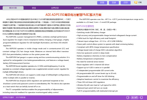
ADP5350主要特性
• 控制多达4通道LED灯串(如红,绿,蓝,白或白×4等) • Switching mode USB battery charger • High accuracy and programmable charge terminal voltageand charge current • 3 MHz buck for high efficiency and small footprint • Tolerant input voltage from −0.5 V to +20 V (USB VVBUSx) • Power path control allows system to operate with dead ormissing battery • Compliant with JEITA charge temperature specification • Voltage-based state of charge (SOC) calculation algorithm • Extra low quiescent current in sleep mode • Battery impedance chemistry (Li-Ion) compensation • Battery temperature compensation • No need for external sense resistor • Boost regulator with 5-channel LED driver • Support up to 4 LED in series or in parallel • 5 independent programmable LED current sinks • 64 programmable LED current levels (up to 20 mA) • Programmable on and off timer for LED blinking • Adaptive headroom control to maximize the efficiency • Three 150 mA linear LDO regulators • Ultralow IQ with zero load at 1 μA typical for LDO1 • Optional load-switch full turn-on mode • Full I2C programmability with dedicated interrupt pin
METSEPM5350电流电压表选型手册
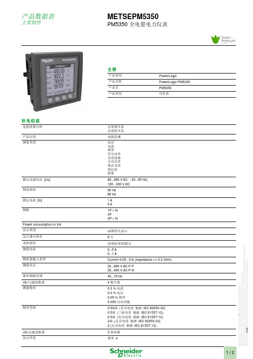
环境
电磁兼容性 ● 抗辐射, 符合 IEC 61000-4-3 ● 抗快速瞬变, 符合 IEC 61000-4-4 ● 抗浪涌, 符合 IEC 61000-4-5 ● 抗导电, 符合 IEC 61000-4-6 ● 振荡波抗扰度试验, 符合 IEC 61000-4-12 ● 谐波发射, 符合 IEC 61000-3-2 ● 闪烁发射, 符合 IEC 61000-3-3 ● 抗静电干扰, 符合 IEC 61000-4-2 ● 传导和辐射干扰 等级 A类, 符合 EN 55011 III IP30 (后面) 符合 IEC 60529 IP51 (前面板) 符合 IEC 60529 0...95 % 50 °C 2 -40...85 °C -25...70 °C 0...3000 m
Contrac/2
额定电源电压 [Us] 网络频率 额定电流 [In] 极数
Power consumption in VA 显示类型 显示器分辨率 采样频率 测量电流 模拟量输入类型 测量电压 频率测量范围 (输入)通道数量 测量精度 LCD背光显示 6行 每周波采样32点 0...5 A 0...1 A Current 0.05...9 A (impedance <= 0.3 Ohm) 20...690 V AC P-P 20...400 V AC P-N 45...70 Hz 4 数字量 0.3 % 电流 0.3 % 电压 0.05 % 频率 0.005 功率因数 0.5S级 (有功电度 根据 IEC 62053-22) 0.5级 (三相功率 根据 IEC 61557-12) 0.5级 (有功电度 根据 IEC 61557-12) 3级 (无功电度 根据 IEC 62053-23) 2 (无功电度 根据 IEC 61557-12) 2 继电器 费率 4
5350中文资料

SMOKE DETECTOR WITH INTERCONNECTThe A5350CA is a low-current, CMOS circuit providing all of the required features for an ionization-type smoke detector. A networking capability allows as many as 125 units to be interconnected so that if any unit senses smoke, all units will sound an alarm. In addition,special features are incorporated to facilitate alignment and test of the finished smoke detector. This device is designed to comply with Underwriters Laboratories Specification UL217.The internal oscillator and timing circuitry keeps standby power to a minimum by powering down the device for 1.66 seconds and sensing smoke for only 10 ms. Every 24 on/off cycles, a check is made for low battery condition. By substituting other types of sensors, or a switch for the ionization detector, this very-low power device can be used in numerous other battery-operated safety/security applications.The A5350CA is supplied in a low-cost, 16-pin dual in-line plastic package. It is rated for continuous operation over the temperature range of 0°C to +50°C.FEATURESs Interconnect Up to 125 Detectors s Piezoelectric Horn Drivers Guard Outputs for Detector Input s Pulse Testing for Low Battery s Power-ON Resets Internal Reverse Battery ProtectionAlways order by complete part number: A5350CA .Data Sheet26110.5*115 Northeast Cutoff, Box 15036Worcester, Massachusetts 01615-0036 (508) 853-5000WCopyright © 1995, 1999, Allegro MicroSystems, Inc.ELECTRICAL CHARACTERISTICS at T A = +25°C, V DD = 9.0 V, V SS = 0 V, C 12 = 0.1 µF,R 7 = 8.2 M Ω (unless otherwise noted).NOTE 1:Negative current is defined as coming out of (sourcing) the specified device pin.NOTE 2:Alarm (Smoke) Condition is defined as V 15 > V 13; No Alarm (No Smoke) Condition as V 15 < V 13.Test LimitsCharacteristic Pin Test Conditions Min.Typ.Max.Units Supply Voltage Range 6Operating6.09.012V Detector Input Current 150 to 40% RH, V IN = 0 to 9.0 V ——±1.0pA Input Offset Voltage14-15Active Guard ——±100mV 16-15Active Guard ——±100mV 15-13Detect Comparator ——±50mV Common Mode Range14-15Guard Amplifier 2.0—V DD - 0.5V 13-15Smoke Comparator 0.5—V DD - 2.0V Active Guard Impedance14to V SS —10—k Ω16to V SS —500—k Ω Oscillator Period12No Alarm 1.34 1.67 2.00s Alarm324048ms Oscillator Pulse Width 128.01012ms Low Voltage Threshold 6T A = 0 to 50°C7.2—7.8V Horn Output Voltage10-11I OUT = 16 mA, V DD = 9.0 V —0.10.5V I OUT = 16 mA, V DD = 7.2 V ——0.9V I OUT = -16 mA, V DD = 9.0 V 8.58.8—V I OUT = -16 mA, V DD = 7.2 V6.3——V Horn Output ON Time10-11Alarm 120160208ms Low Battery8.01012ms Horn Output OFF Time10-11Alarm 6080104ms Low Battery324048s LED Output ON Current 5V DD = 7.2 V, V OUT = 1.0 V10——mA LED Output ON Time 58.01012ms LED Output OFF Time 5No Alarm, In Standby 324048s I/O Current2No Alarm, V I/O = V DD - 2.0 V 25—60µA Alarm, V I/O = V DD - 2.0 V-7.5——mA I/O Alarm Voltage 2External “Alarm” In 3.0——V I/O Delay 2“Alarm” Out— 3.0—s Supply Current6V DD = 9.0 V, No Alarm, No Loads — 5.09.0µA V DD = 12 V, No Alarm, No Loads——12µA115 Northeast Cutoff, Box 15036Worcester, Massachusetts 01615-0036 (508) 853-5000The A5350CA is a low-current CMOS circuit providing all of the required features for an ionization-type smoke detector.Oscillator. An internal oscillator operates with a period of 1.67 seconds during no-smoke conditions. Every 1.67seconds, internal power is applied to the entire circuit and a check is made for smoke. Every 24 clock cycles (40seconds), the LED is pulsed and a check is made for low battery by comparing V DD to an internal reference.Since very-low currents are used in the device, theoscillator capacitor at pin 12 should be a low-leakage type (PTFE, polystyrene, or polypropylene).Detector Circuitry. An active guard is provided on both pins adjacent to the detector input (pin 15). The voltage at pins 14 and 16 will be within 100 mV of the input. This will keep surface leakage currents to a minimum and provide a method of measuring the input voltage without loading the ionization chamber. The active guard ampli-fier is not power strobed and thus provides constant protection from surface leakage currents. The detector input has internal diode protection against static damage.Alarm Circuitry. If smoke is detected, the oscillator period changes to 40 ms and the horn is enabled. The horn output is typically 160 ms ON, 80 ms OFF. During the OFF time, smoke is again checked and will inhibit further alarm output if smoke is not sensed. During smoke conditions the low battery alarm is inhibited and the LED is driven at a 1 Hz rate.Sensitivity Adjust. The detector sensitivity must be externally adjusted to the individual characteristics of the ionization chamber by connecting resistors between pin 13 and V DD , and between pin 13and V SS .Low Battery. The low battery threshold is set internally by a voltage divider connected between V DD and V SS .The threshold can be increased by connecting a resistor between pin 3 and V DD . The threshold can be decreased by connecting a resistor between pin 3 and V SS . The battery voltage level is checked every 40 seconds during the 10 mA, 10 ms LED pulse. If an LED is not used, it should be replaced with an equivalent resistor (typically 500 Ω to 1000 Ω) such that the battery loading remains at 10 mA.I/O. A connection is provided at pin 2 to allow multiple smoke detectors to be commoned. If any single unitdetects smoke (I/O is driven high), all connected units will sound their associated horns after a nominal 3 second delay. The LED is suppressed when an alarm is signaled from an interconnected unit.Testing. On power up, all internal counters are reset.Internal test circuitry allows for low battery check byholding pins 8 and 12 low during power up, then reducing V DD and monitoring HORN 1 (pin 10). All functional tests can be accelerated by driving pin 12 with a 2 kHz square wave. The 10 ms strobe period must be maintained for proper operation of the comparator circuitry.CIRCUIT DESCRIPTIONDwg. WC-003-1TYPICAL APPLICATIONTIMING DIAGRAMS IN TYPICAL APPLICATIONNOTE 1:An external resistor divider is used to adjust sensitivity for the particularsmoke chamber.NOTE 2: A resistor to ground or V DD may be added to this pin to modify lowbattery voltage threshold.Dwg. EC-005-3V15 < V13 (NO SMOKE)V15 > V13 (SMOKE)V12OSC. CAPINTERNAL CLOCKLED SMOKE COMPARATORSMOKE CHAMBERHORN115 Northeast Cutoff, Box 15036Worcester, Massachusetts 01615-0036 (508) 853-5000Dwg. WC-004HORN ONOFFHORN NOT SELF COMPLETING WHEN IN REMOTE ONLY ALARMINTERNAL CLOCKHORNV2 IN I/O4 CYCLES 2 CYCLES40 ms1.67 s72 CLOCK CYCLESV2 OUT I/OINTERNAL CLOCKLOCAL ALARM MODEREMOTE ALARM MODEHORN ONOFFHORNI/O OPERATIONDimensions in Inches (controlling dimensions)Dimensions in Millimeters(for reference only) NOTES:1.Lead thickness is measured at seating plane or below.2.Lead spacing tolerance is non-cumulative.3.Exact body and lead configuration at vendor’s option within limits shown.Dwg. MA-001-16A inDwg. MA-001-16A mm115 Northeast Cutoff, Box 15036Worcester, Massachusetts 01615-0036 (508) 853-5000Allegro MicroSystems, Inc. reserves the right to make, from time to time, such departures from the detail specifications as may be required to permit improvements in the design of its products.The information included herein is believed to be accurate and reliable. However, AllegroMicroSystems, Inc. assumes no responsibility for its use; nor for any infringements of patents or other rights of third parties which may result from its use.SAFETY & SECURITY ICsSELECTION GUIDEPart Number FunctionA3054KU/SU Multiplexed Two-Wire Hall-Effect SensorA5348CA Ionization-Type Smoke Detector with Interconnect, Timer, and Reverse-Battery Protection A5349CA Ionization-Type Smoke Detector with Interconnect and Timer for AC Line Operation A5350CA Ionization-Type Smoke Detector with Interconnect and Reverse-Battery Protection A5354CA Ionization-Type Smoke Detector with Interconnect and Reverse-Battery Protection A5358CA Photoelectric-Type Smoke Detector with Interconnect and TimerA5364CA Ionization-Type Smoke Detector with Interconnect, Reverse-Battery Protection,and Temporal Horn PatternA5368CAIonization-Type Smoke Detector with Interconnect, Timer, Reverse-Battery Protection,and Temporal Horn Pattern。
FAN5350资料
July 2007 Chip-Scale and MLP PackagingFeatures3MHz Fixed-Frequency Operation16µA Typical Quiescent Current600mA Output Current Capability2.7V to 5.5V Input Voltage Range1.82V Fixed Output VoltageSynchronous OperationPower-Save ModeSoft-Start CapabilityInput Under-Voltage Lockout (UVLO)Thermal Shutdown and Overload Protection 6-Lead 3 x 3mm MLP5-Bump 1 x 1.37mm WLCSPApplicationsCell Phones, Smart-PhonesPocket PCsWLAN DC-DC Converter ModulesPDA, DSC, PMP, and MP3 PlayersPortable Hard Disk Drives DescriptionThe FAN5350 is a step-down switching voltage regulator that delivers a fixed 1.82V from an input voltage supply of 2.7V to 5.5V. Using a proprietary architecture with synchronous rectification, the FAN5350 is capable of delivering 600mA at over 90% efficiency, while maintaining a very high efficiency of over 80% at load currents as low as 1mA. The regulator operates at a nominal fixed frequency of 3MHz at full load, which reduces the value of the external components to 1µH for the output inductor and 4.7µF for the output capacitor.At moderate and light loads, pulse frequency modulation is used to operate the device in power-save mode with a typical quiescent current of 16µA. Even with such a low quiescent current, the part exhibits excellent transient response during large load swings. At higher loads, the system automatically switches to fixed-frequency control, operating at 3MHz. In shutdown mode, the supply current drops below 1µA, reducing power consumption.The FAN5350 is available in a 6-lead Molded Leadless Package (MLP) and a 5-bump Wafer Level Chip Scale Package (WLCSP).Ordering InformationPart Number Pb-FreeOperatingTemperature RangePackage PackingMethodFAN5350UCX Yes -40°C to 85°C WLCSP-5 1x1.37mm Tape and Reel(1) FAN5350MPX Yes -40°C to 85°C MLP-6 3 x 3mm Tape and Reel(1) Note:1. Please refer to tape and reel specifications on ; /packaging.3MHz OSCZero CrossingGND Figure 3. Block Diagram2 AGND Analog Ground Pin . Signal ground for the part.3 FB Feedback Analog Input . Connect directly to the output capacitor.4 ENEnable Pin . The device is in shutdown mode when voltage to this pin is <0.4V and enabled when >1.2V. Do not leave this pin floating. 5 SW Switching Node . Connection to the internal PFET switch and NFET synchronous rectifier. 6 V INPower Supply Input .Symbol Parameter Min. Typ. Max. Units ΘJA_WLCSP Junction-to-Ambient Thermal Resistance(2)180 °C/W ΘJA_MLP Junction-to-Ambient Thermal Resistance(2)49 °C/W Note:2. Junction-to-ambient thermal resistance is a function of application and board layout. This data is measured withfour-layer 1s2p boards in accordance to JESD51- JEDEC standard. Special attention must be paid not to exceed junction temperature T J(max) at a given ambient temperate T A.Decrease DecreaseIncrease Increase Improved Table 1. Effects of changes in inductor value (from 1µH recommended value) on regulator performanceto 10µF helps significantly. Figure 7. The FAN5350 Evaluation Board PCB (CSP)1.501.251.000.750.500.25000.10.20.30.40.50.60.70.80.9 1.01.1Load Current (A)O u t p u t V o l t a g e (V )V IN =5.5VV IN =3.6VINAmbient Temperature (°C)O u t p u t V o l t a g e (m V 180018051810181518201825V IN =5.5VV IN =3.6VV IN =2.7V-40-20020406080I LOAD =300mAFigure 12. DC Current Voltage Output Characteristics Figure 13. Output Voltage vs. Temperature/div35dB1Hz 10Hz 100Hz 1kHz 10kHz2.72.82.92.7 2.93.1 3.3 3.5 3.7 3.94.1 4.3 4.5 4.7 4.95.1 5.3 5.5 FrequenBattery Voltage (V)+85°CFigure 18. Power Supply Rejection Ratio in CCM Figure 19. Switching Frequency in CCMI LOAD = 600mA I LOAD = 300mA I LOAD = 50mA I LOAD = 1mAH scale: 20µs / di v.H scale: 20µs / di v.Figure 24. Fast Load Transient in CCM Figure 25. Fast Load Transient in DCMV OUT(ac), 20mV / div.I L = 0.2A / div.V SW , 2V / div.V OUT(ac), 20mV / div.I L = 0.1A / div.V SW , 2V / div.H scale: 1µs / di v.H scale: 200µs / di v.Figure 31. Typical Waveforms in DCM, 50mA LoadFigure 32. Typical Waveforms in CCM, 150mA LoadFigure 33. 6-Lead Molded Leadless Package (MLP)Product Specific DimensionsProduct D E X Y FAN5350UCX 1.370 +/- 0.030 1.000 +/- 0.030 0.270 0.272Figure 34. 5-Bump Wafer-Level Chip-Scale Package (WLCSP)FAN5350 — 3MHz, 600mA Step-Down DC-DC Converter in Chip-Scale and MLP Packaging。
智能变电站光数字测试仪说明书
目录1. 前言 (1)1.1关于本说明书 (1)1.2安全须知 (1)1.3产品清单 (2)1.4责任声明 (3)2. 概述 (4)2.1功能说明 (4)2.2性能参数 (4)2.2.1基本性能 (4)2.2.2接收性能 (4)2.2.3发送性能 (5)3. 技术参数 (6)3.1环境条件 (6)3.2机械尺寸及重量 (6)3.3电源 (6)3.4电磁兼容性能 (6)4. 操作说明 (7)4.1外观布局 (7)4.1.1接口 (8)4.1.2指示灯 (8)4.1.3按键 (9)4.2开机关机 (10)4.2.1开机 (10)4.2.2HOME菜单 (10)4.2.3锁定 (10)4.2.4关机 (11)4.3主界面 (13)5. 系统设置 (14)5.1基本设置 (14)5.2连接管理 (14)5.3存储器 (15)5.4备份还原 (16)5.5关于 (17)6. 参数配置 (18)6.1基本参数 (18)6.2SMV发送 (19)6.3GOOSE发送 (25)6.4GOOSE接收 (31)7. 手动试验 (36)7.1扩展菜单 (37)7.1.1SMV映射表 (38)7.1.2开入映射表 (40)7.1.3通道品质 (41)7.1.4状态字 (41)7.1.5异常设置 (42)7.1.6显示开入量 (42)7.1.7设置 (43)7.1.8试验结果 (45)8. 状态序列 (49)8.1状态设置 (49)8.1.1故障计算 (52)8.1.2谐波设置 (53)8.2扩展菜单 (54)9. SMV接收 (56)9.1SMV探测 (56)9.2有效值 (57)9.3波形 (62)9.4相量 (63)9.5序量 (64)9.6功率 (65)9.7谐波 (66)9.8双AD (67)9.9核相 (68)9.10极性 (70)9.11MU延时 (71)9.12报文统计 (72)9.13报文监测 (74)9.13.1SCL配置与报文比较 (74)9.13.2报文录波 (74)10. GOOSE接收 (79)10.1GOOSE探测 (79)10.2实时值 (80)10.3变位列表 (82)10.4报文统计 (84)10.5报文监测 (86)10.6间隔监测 (88)11. 录波分析 (89)11.1录制报文 (89)11.2加载文件 (91)12. 对时 (92)12.1对时功能 (92)12.2授时功能 (93)13. 网络压力 (94)13.1网络压力测试 (94)13.2网络流量统计 (95)14. 光功率 (96)15. SCL编辑器 (97)15.1主界面介绍 (97)15.2SMV/GOOSE控制块信息视图区 (97)15.2.1SMV信息视图 (98)15.2.2GOOSE信息视图 (100)15.3导入SCL或SCX文件 (102)15.4导出配置 (103)15.5SMV/GOOSE信息另存为 (103)15.6SMV/GOOSE信息切换 (104)15.7编辑SMV/GOOSE 信息 (104)15.8查找IED (108)16. 使用示例 (109)16.1示例1——IEC60044-7/8报文发送及GOOSE动作信号接收(手动试验) . 10916.2示例2——通过交换机发IEC61850-9-2,收GOOSE信号(状态序列) (110)16.3示例3——接收IEC60044-7/8报文 (111)16.4示例4——接收IEC61850-9-1/2 报文 (112)16.5示例5——接收GOOSE报文 (113)1. 前言1.1 关于本说明书本说明书提供如何以安全的方式使用GDDT6000智能变电站光数字测试仪的准确信息,说明书中详细介绍了安全、规范的操作要领以及各种测量功能的使用流程,请您在使用协议前完整的阅读完本说明书。
AA5305S中文资料
Single Color φ5 Round Shape Type5305S SeriesSpatial Distribution ExampleCondition : Ta = 25℃Spectral DistributionRelative Intensity vs. WavelengthCondition : Ta = 25℃, I F = 20mAWavelength [nm]R e l a t i v e I n t e n s i t yForward Voltage vs. Forward CurrentCondition : Ta = 25℃Forward Voltage V F (V)F o r w a r d C u r r e n t I F (m A )Forward Current vs. Relative IntensityCondition : Ta = 25℃Forward Current I F (mA)R e l a t i v e I n t e n s i t yTechnical Data (EBG/BG)FSingle Color φ5 Round Shape Type5305S SeriesSpatial Distribution ExampleCondition : Ta = 25℃Spectral DistributionRelative Intensity vs. WavelengthCondition : Ta = 25℃, I F = 20mAWavelength [nm]R e l a t i v e I n t e n s i t yForward Voltage vs. Forward CurrentCondition : Ta = 25℃Forward Voltage V F (V)F o r w a r d C u r r e n t I F (m A )Forward Current vs. Relative IntensityCondition : Ta = 25℃Forward Current I F (mA)R e l a t i v e I n t e n s i t yTechnical Data (EPG/PG)FSingle Color φ5 Round Shape Type5305S SeriesSpatial Distribution ExampleCondition : Ta = 25℃Spectral DistributionRelative Intensity vs. WavelengthCondition : Ta = 25℃, I F = 20mAWavelength [nm]R e l a t i v e I n t e n s i t yForward Voltage vs. Forward CurrentCondition : Ta = 25℃Forward Voltage V F (V)F o r w a r d C u r r e n t I F (m A )Forward Current vs. Relative IntensityCondition : Ta = 25℃Forward Current I F (mA)R e l a t i v e I n t e n s i t yTechnical Data (EPY/PY)FSingle Color φ5 Round Shape Type5305S SeriesSpatial Distribution ExampleCondition : Ta = 25℃Spectral DistributionRelative Intensity vs. WavelengthCondition : Ta = 25℃, I F = 20mAWavelength [nm]R e l a t i v e I n t e n s i t yForward Voltage vs. Forward CurrentCondition : Ta = 25℃Forward Voltage V F (V)F o r w a r d C u r r e n t I F (m A )Forward Current vs. Relative IntensityCondition : Ta = 25℃Forward Current I F (mA)R e l a t i v e I n t e n s i t yTechnical Data (EAY/AY)FSingle Color φ5 Round Shape TypeSpatial Distribution ExampleCondition : Ta = 25℃Spectral DistributionRelative Intensity vs. WavelengthCondition : Ta = 25℃, I F = 20mAWavelength [nm]R e l a t i v e I n t e n s i t yForward Voltage vs. Forward CurrentCondition : Ta = 25℃Forward Voltage V F (V)F o r w a r d C u r r e n t I F (m A )Forward Current vs. Relative IntensityCondition : Ta = 25℃Forward Current I F (mA)R e l a t i v e I n t e n s i t yTechnical Data (EAA/AA)5305S SeriesFSingle Color φ5 Round Shape Type5305S SeriesSpatial Distribution ExampleCondition : Ta = 25℃Spectral DistributionRelative Intensity vs. WavelengthCondition : Ta = 25℃, I F = 20mAWavelength [nm]R e l a t i v e I n t e n s i t yForward Voltage vs. Forward CurrentCondition : Ta = 25℃Forward Voltage V F (V)F o r w a r d C u r r e n t I F (m A )Forward Current vs. Relative IntensityCondition : Ta = 25℃Forward Current I F (mA)R e l a t i v e I n t e n s i t yTechnical Data (EVR/VR)FCondition : Ta = 25℃Wavelength[nm]Forward Current vs. Relative IntensityFCondition : Ta = 25℃Wavelength[nm]Forward Current vs. Relative IntensityF。
Y220S用户指南_Y220-T10_01_中文_中国移动
3. 通话功能...................................................................... 16
3.1 拨打电话 .............................................................................. 16 3.2 接听或拒接电话 ................................................................... 17 3.3 通话中的其他操作 ................................................................ 18 3.4 使用通话记录 ....................................................................... 19 3.5 使用飞行模式 ....................................................................... 19
4. 联系人 ......................................................................... 20
4.1 打开通讯录 .......................................................................... 20 4.2 从 USIM 卡或 SIM 卡复制联系人信息 .................................. 20 4.3 创建联系人信息 ................................................................... 20
- 1、下载文档前请自行甄别文档内容的完整性,平台不提供额外的编辑、内容补充、找答案等附加服务。
- 2、"仅部分预览"的文档,不可在线预览部分如存在完整性等问题,可反馈申请退款(可完整预览的文档不适用该条件!)。
- 3、如文档侵犯您的权益,请联系客服反馈,我们会尽快为您处理(人工客服工作时间:9:00-18:30)。
−103 handbook, halfpage VCEsat (mV) −102
(1)
MGW169
handbook, halfpage
−1.4 VBEsat (V) −1.2 −1.0 − 0.8
MGW170
(1) (2)
(2) (3)
−10
− 0.6
(3)
− 0.4 − 0.2 −10 −1
−1 −10 −1
2003 May 13
5
Philips Semiconductors
Product specification
50 V low VCEsat PNP transistor
Fig.4
Collector-emitter saturation voltage as a function of collector current; typical values.
Fig.5
Base-emitter saturation voltage as a function of collector current; typical values.
PBSS5350Z
MAX. −60 −50 −6 −3 −5 −1 1.35 2 +150 150 +150 V V V A A A W W
UNIT
°C °C °C
1. Device mounted on a printed-circuit board; single sided copper; tinplated; mounting pad for collector 1 cm2. 2. Device mounted on a printed-circuit board; single sided copper; tinplated; mounting pad for collector 6 cm2. 3. For other mounting conditions see “Thermal considerations for SOT223 in the General Part of associated Handbook”. THERMAL CHARACTERISTICS SYMBOL Rth j-a PARAMETER thermal resistance from junction to ambient CONDITIONS in free air; notes 1 and 3 in free air; notes 2 and 3 Notes 1. Device mounted on a printed-circuit board; single sided copper; tinplated; mounting pad for collector 1 cm. 2. Device mounted on a printed-circuit board; single sided copper; tinplated; mounting pad for collector 6 cm2. 3. For other mounting conditions see “Thermal considerations for SOT223 in the General Part of associated Handbook”. VALUE 92 62.5 UNIT K/W K/W
VCE = −2 V. (1) Tamb = −55 °C. (2) Tamb = 25 °C. (3) Tamb = 150 °C.
Fig.2
DC current gain as a function of collector current; typical values.
Fig.3
Base-emitter voltage as a function of collector current; typical values.
2003 May 13
3
Philips Semiconductors
Product specification
50 V low VCEsat PNP transistor
CHARACTERISTICS Tamb = 25 °C unless otherwise specified. SYMBOL ICBO IEBO hFE PARAMETER CONDITIONS − − − 200 200 100 − − − − − − 100 − VCB = −50 V; IE = 0; Tj = 150 °C emitter-base cut-off current DC current gain VEB = −5 V; IC = 0 VCE = −2 V; IC = −500 mA IC = −1 A; note 1 IC = −2 A; note 1 VCEsat collector-emitter saturation voltage IC = −500 mA; IB = −50 mA IC = −1 A; IB = −50 mA IC = −2 A; IB = −200 mA; note 1 RCEsat VBEsat VBEon fT Cc Note 1. Pulse test: tp ≤ 300 µs; δ ≤ 0.02. equivalent on-resistance base-emitter saturation voltage transition frequency collector capacitance IC = −2 A; IB = −200 mA; note 1 IC = −2 A; IB = −200 mA; note 1 − − − − − − 120 − − − − MIN. − − −
Philips Semiconductors
Product specification
50 V low VCEsat PNP transistor
FEATURES • Low collector-emitter saturation voltage • High collector current capability: IC and ICM • High collector current gain (hFE) at high IC • Higher efficiency leading to less heat generation • Reduced PCB area requirements compared to DPAK. APPLICATIONS • Power management – DC/DC converters – Supply line switching – Battery charger – Linear voltage regulation (LDO). • Peripheral drivers – Driver in low supply voltage applications, e.g. lamps, LEDs – Inductive load driver, e.g. relays, buzzers, motors. DESCRIPTION PNP low VCEsat transistor in a SOT223 plastic package. NPN complement: PBSS4350Z.
4
2, 4 1 3
Top view
MAM288
MARKING TYPE NUMBER PBSS5350Z MARKING CODE PB5350 Fig.1
Simplified outline (SOT223) and symbol.
2003 May 13
2
Philips Semiconductors
(2)
− 0.4 200
(3)
(3)
0 −10 −1
−1
−10
−102
−103 −104 I C (mA)
0 −10 −1
−1
−10
−102
−103 −104 I C (mA)
VCE = −2 V. (1) Tamb = 150 °C. (2) Tamb = 25 °C. (3) Tamb = −55 °C.
1 2 3
handbook, halfpage
PBSS5350Z
QUICK REFERENCE DATA SYMBOL VCEO IC ICM RCEsat PINNING PIN 1 2 3 4 base collector emitter collector DESCRIPTION PARAMETER collector-emitter voltage collector current (DC) peak collector current equivalent on-resistance MAX. −50 −3 −5 <150 UNIT V A A mΩ
Product specification
50 V low VCEsat PNP transistor
PBSS5350Z
handbook, halfpage
1000
MGW167
handbook, halfpage
− 1.2
MGW168
hFE 800
(1)
VBE (V) − 0.8
(1)
600
(2)
400
base-emitter turn-on voltage VCE = −2 V; IC = −1 A; note 1 IC = −100 mA; VCE = −5 V; f = 100 MHz VCB = −10 V; IE = Ie = 0; f = 1 MHz
2003 May 13
4
Philips Semiconductors
−1
−10
−102
−103 −104 I C (mA)
−1
−10