lm25017
故障码解析1

1.运行DTC的条件
*无启动的TP、MAP、IAT、ECT、MAF、CKP传感器、缺火、燃油喷嘴电路、EVAP、EGR的故障码DTC存在;
*闭环指令的空燃比在14.4和14.9之间;
*节气门角度在5%和40%之间。
2.设定DTC的条件
*正常的闭环操作期间,HO2S信号电压始终低于175mV或在(混合气加浓)动力增强模式燃油控制操 作期间,HO2S信号电压始终低于600mV;
仔细察看诊断故障代码设置条件的重要意义就在于:作为车辆的维修人员,你必须知道这辆车的故障到底是什么时候发生的?故障码是因为什么条件而触发的?自己应该怎样才能模拟故障发生的条件?
怎样确定故障真正被排除了
故障码告诉你现在或过去该车的某某系统出现了某某故障,那么只要在维修结束后,该故障码不再出现也就说明故障被排除了。但是请记住,故障码可以因为故障不存在而消失,同样如果故障监测系统程序因为某些条件的制约而被中止,故障码一样是不会出现的。以上海通用别克轿车装备的OBD-Ⅱ系统为例。要完成整个系统的所有项目检测至少要经过12min,而且在这12min内必须按照OBD-Ⅱ的检测要求执行:怠速、加速、巡航、再加速、再次高速巡航、无制动滑行等一些特定工况。这种连续工况检测被称为一个OBD-Ⅱ驱动循环或15工况。只有经过了这样的一个驱动循环,所有的监测器才都开动,过了检测,并且在控制模块中记录下了I/M标志,表明整个系统的检测情况。由于个人驾驶习惯、行驶路况等原因,在修理结束之后的试车过程中如果恰好该系统的监测器未被开动,那么故障代码就自然不会出现。所以,修理工作完成后千万要按照原先设置代码的条件,避开制约该监测器开动的种种因素进行试车检验。如果有SGM TECH 2诊断仪,那么通过进入特定DTC菜单观看故障监测状态是非常有必要的。
Buck Converters Provide a Battery Charger and System Power

LM2574,LM2576,LM2594,LM2596,LMC6482, LMC7101Buck Converters Provide a Battery Charger and System PowerLiterature Number: SNVA532Buck-converter Charger also Provides System PowerRobert Hanrahan - National Semiconductor11/16/96 Many systems require long time operation during periods of power loss. Often a Lead Acid battery (gel or wet-cell) is found to be the best solution because of the high capacity and relative low cost. The battery is charged during normal operation, and used to power the system during power loss. These systems require a circuit to charge the battery as well as regulate voltage for the system Vcc. In these systems one must provide a current limited voltage to the battery for charging, while developing system Vcc in both the charge or discharge condition.Many older designs would utilize inefficient linear regulators to provide these functions. These designs require a large heat sink for regulating the battery voltage to the system Vcc (typically 5V).One may utilize switching regulator technology to provide a much more efficient design at about the same relative cost as a linear regulator design. Many of these designs utilize low voltage AC power that is usually provided by a low cost wall transformer. Because of the switching technology utilized in this design, one could accommodate a wide input voltage range and thus may be used for power line voltages from 100V to 240V without any circuit changes.One of the best approaches to the design is a current limited voltage source that sources current into the battery until the battery voltage reaches a voltage setpoint. The charger then operates in a constant voltage mode, supplying the current required to maintain the voltage.Most lead acid batteries have a voltage setpoint of 13.8V at 25o C. The current limit is set depending on the exact battery and charge time requirement.The design shown in Figure 1 employs two Simple Switcher Buck converters from National Semiconductor. The first regulator U1 is an LM2576 or LM2596 Simple Switcher used to efficiently step down the unregulated input voltage from the output of the rectifier. This buck converter generates the input voltage for the battery while also providing voltage to the second regulator. Both buck regulators may utilize either a slower 52 kHz converter or a higher frequency device marked respectively. The higher frequency devices employ added features such as sync input and soft-start. The second regulator U2, is a small DIP or SO LM2574 or LM2594 capable of providing up to 0.5A system Vcc. One must consider the system current requirements when setting the current limit value of the charger. The current limit value set by the gain of U3 must be increased by the current required to supply power to the system.The first regulator provides the charge voltage setpoint with current regulation while the second regulator provides the system VccFIGURE 1.U1 is regulated at the Battery charge voltage with the feedback network R1/R2. These resistors are chosen by Vout=1.23(1+R2/R1). The diode D3 provides current switching between U1 and the battery during power loss.The shaded area is used to measure and regulate the current flow into the battery during battery charge. The circuit utilizes a shunt resistor to measure the current to the battery, and amplifies it via the amplifier U3. The LMC7101 shown for U3 is a National Semiconductor CMOS OP-Amp that provides an output voltage inversely proportional to current. The LMC7101 provides a BW of 1 MHz and is available in a very small SOT23 package. Other Op-Amps such as the National LMC6482 will also do the job, and are available in standard DIP and SO packages.With the gain of 10 provided by the Op-Amp, the diode D2 will forward bias and pull up the feedback voltage when the output current is about 1.6A (Vref+diode drop). During normal voltage regulation the diode is reverse biased.The second regulator U2 is used to provide 5V to the system. This buck regulator efficiently provides system power when the input is at its highest voltage of about 13.8V or at the lower voltage that will be generated when U1 is current limiting .An additional SOT23 comparator and voltage reference provides a battery chargeindication.FIGURE 2.Some systems may need an indication of charge complete. In a system that utilizes a microcontroller with on chip A/D (such as the National COP8ACC), one could connect the output of U3 into the input of the A/D, and read the charge current directly. Depending of the voltage reference used for the A/D, and accuracy needed, one may need to add another Op-Amp stage prior to the A/D. Figure 2 shows the circuit with an added SOT23 voltage comparator. The output of the current amplifier U2 is compared to the voltage set by the potentiometer R9. This voltage can be set to represent the current flow that takes place at the end of charge.Simple Switcher designs can be analyzed and verified by utilizing a software package called “Switchers Made Simple” from National Semiconductor. By splitting the design into two buck voltage regulators, one may utilize the software to obtain component values with vendor part numbers, junction temperatures, stability, and lots more design information.The software package is available free of charge by calling National at 1-800-272-9959 or through the Web site at .IMPORTANT NOTICETexas Instruments Incorporated and its subsidiaries(TI)reserve the right to make corrections,modifications,enhancements,improvements, and other changes to its products and services at any time and to discontinue any product or service without notice.Customers should obtain the latest relevant information before placing orders and should verify that such information is current and complete.All products are sold subject to TI’s terms and conditions of sale supplied at the time of order acknowledgment.TI warrants performance of its hardware products to the specifications applicable at the time of sale in accordance with TI’s standard warranty.Testing and other quality control techniques are used to the extent TI deems necessary to support this warranty.Except where mandated by government requirements,testing of all parameters of each product is not necessarily performed.TI assumes no liability for applications assistance or customer product design.Customers are responsible for their products and applications using TI components.To minimize the risks associated with customer products and applications,customers should provide adequate design and operating safeguards.TI does not warrant or represent that any license,either express or implied,is granted under any TI patent right,copyright,mask work right, or other TI intellectual property right relating to any combination,machine,or process in which TI products or services are rmation published by TI regarding third-party products or services does not constitute a license from TI to use such products or services or a warranty or endorsement e of such information may require a license from a third party under the patents or other intellectual property of the third party,or a license from TI under the patents or other intellectual property of TI.Reproduction of TI information in TI data books or data sheets is permissible only if reproduction is without alteration and is accompanied by all associated warranties,conditions,limitations,and notices.Reproduction of this information with alteration is an unfair and deceptive business practice.TI is not responsible or liable for such altered rmation of third parties may be subject to additional restrictions.Resale of TI products or services with statements different from or beyond the parameters stated by TI for that product or service voids all express and any implied warranties for the associated TI product or service and is an unfair and deceptive business practice.TI is not responsible or liable for any such statements.TI products are not authorized for use in safety-critical applications(such as life support)where a failure of the TI product would reasonably be expected to cause severe personal injury or death,unless officers of the parties have executed an agreement specifically governing such use.Buyers represent that they have all necessary expertise in the safety and regulatory ramifications of their applications,and acknowledge and agree that they are solely responsible for all legal,regulatory and safety-related requirements concerning their products and any use of TI products in such safety-critical applications,notwithstanding any applications-related information or support that may be provided by TI.Further,Buyers must fully indemnify TI and its representatives against any damages arising out of the use of TI products in such safety-critical applications.TI products are neither designed nor intended for use in military/aerospace applications or environments unless the TI products are specifically designated by TI as military-grade or"enhanced plastic."Only products designated by TI as military-grade meet military specifications.Buyers acknowledge and agree that any such use of TI products which TI has not designated as military-grade is solely at the Buyer's risk,and that they are solely responsible for compliance with all legal and regulatory requirements in connection with such use. TI products are neither designed nor intended for use in automotive applications or environments unless the specific TI products are designated by TI as compliant with ISO/TS16949requirements.Buyers acknowledge and agree that,if they use any non-designated products in automotive applications,TI will not be responsible for any failure to meet such requirements.Following are URLs where you can obtain information on other Texas Instruments products and application solutions:Products ApplicationsAudio /audio Communications and Telecom /communicationsAmplifiers Computers and Peripherals /computersData Converters Consumer Electronics /consumer-appsDLP®Products Energy and Lighting /energyDSP Industrial /industrialClocks and Timers /clocks Medical /medicalInterface Security /securityLogic Space,Avionics and Defense /space-avionics-defense Power Mgmt Transportation and Automotive /automotiveMicrocontrollers Video and Imaging /videoRFID OMAP Mobile Processors /omapWireless Connectivity /wirelessconnectivityTI E2E Community Home Page Mailing Address:Texas Instruments,Post Office Box655303,Dallas,Texas75265Copyright©2011,Texas Instruments Incorporated。
低噪声、高电压皮安级输入精密运算放大器

低噪声、高电压皮安级输入精密运算放大器
佚名
【期刊名称】《电子设计工程》
【年(卷),期】2009(17)9
【摘要】Intersil公司推出首款采用该公司新的专利双极工艺技术的运算放大器ISL28207。
Intersil的ISL28207是双40V低功耗双极精密运算放大器,具有出色的直流精度和极好的温漂性能。
【总页数】1页(P127-127)
【关键词】运算放大器;Intersil公司;低噪声;高电压;输入;双极工艺;低功耗
【正文语种】中文
【中图分类】TN722.77;TP333.4
【相关文献】
1.低电压CMOS模拟集成运算放大器输入级的研究 [J], 俞学刚;程梦璋
2.一种高共模输入范围高输出电压摆幅的CMOS运算放大器 [J], 牛秀卿;何人人
3.新的Intersil低噪声、高电压皮安级输入精密运算放大器 [J], 无
4.精益求精:世健皮安级评估套件搭载ADI飞安级运算放大器 [J], 董梅
5.低噪声高精度运算放大器输入级的设计 [J], 朱臻;邵志标
因版权原因,仅展示原文概要,查看原文内容请购买。
LM2577-12中文资料

LM1577/LM2577SeriesSIMPLE SWITCHER ®Step-Up Voltage RegulatorGeneral DescriptionThe LM1577/LM2577are monolithic integrated circuits that provide all of the power and control functions for step-up (boost),flyback,and forward converter switching regulators.The device is available in three different output voltage ver-sions:12V,15V,and adjustable.Requiring a minimum number of external components,these regulators are cost effective,and simple to use.Listed in this data sheet are a family of standard inductors and flyback transformers designed to work with these switching regula-tors.Included on the chip is a 3.0A NPN switch and its associated protection circuitry,consisting of current and thermal limiting,and undervoltage lockout.Other features include a 52kHz fixed-frequency oscillator that requires no external compo-nents,a soft start mode to reduce in-rush current during start-up,and current mode control for improved rejection of input voltage and output load transients.Featuresn Requires few external componentsn NPN output switches 3.0A,can stand off 65V n Wide input voltage range:3.5V to 40VnCurrent-mode operation for improved transient response,line regulation,and current limit n 52kHz internal oscillatorn Soft-start function reduces in-rush current during start-up n Output switch protected by current limit,under-voltage lockout,and thermal shutdownTypical Applicationsn Simple boost regulatorn Flyback and forward regulators n Multiple-output regulatorTypical ApplicationOrdering InformationTemperature Range Package TypeOutput VoltageNSC12V 15V ADJ Package Package Drawing −40˚C ≤T A ≤+125˚C24-Pin Surface Mount LM2577M-12LM2577M-15LM2577M-ADJ M24B SO 16-Pin Molded DIP LM2577N-12LM2577N-15LM2577N-ADJ N16A N 5-Lead Surface Mount LM2577S-12LM2577S-15LM2577S-ADJ TS5B TO-2635-Straight Leads LM2577T-12LM2577T-15LM2577T-ADJ T05A TO-2205-Bent Staggered LM2577T-12LM2577T-15LM2577T-ADJ T05DTO-220LeadsFlow LB03Flow LB03Flow LB03−55˚C ≤T A ≤+150˚C4-Pin TO-3LM1577K-12/883LM1577K-15/883LM1577K-ADJ/883K04ATO-3SIMPLE SWITCHER ®is a registered trademark of National Semiconductor Corporation.DS011468-1Note:Pin numbers shown are for TO-220(T)package.June 1999LM1577/LM2577Series SIMPLE SWITCHER Step-Up Voltage Regulator©1999National Semiconductor Corporation Absolute Maximum Ratings (Note 1)If Military/Aerospace specified devices are required,please contact the National Semiconductor Sales Office/Distributors for availability and specifications.Supply Voltage45V Output Switch Voltage65V Output Switch Current (Note 2) 6.0APower DissipationInternally Limited Storage Temperature Range −65˚C to +150˚CLead Temperature (Soldering,10sec.)260˚C Maximum Junction Temperature150˚CMinimum ESD Rating(C =100pF,R =1.5k Ω)2kVOperating RatingsSupply Voltage3.5V ≤V IN ≤40V Output Switch Voltage 0V ≤V SWITCH ≤60VOutput Switch CurrentI SWITCH ≤3.0A Junction Temperature Range LM1577−55˚C ≤T J ≤+150˚C LM2577−40˚C ≤T J ≤+125˚CElectrical Characteristics—LM1577-12,LM2577-12Specifications with standard type face are for T J =25˚C,and those in bold type face apply over full Operating Temperature Range .Unless otherwise specified,V IN =5V,and I SWITCH =0.LM1577-12LM2577-12Units SymbolParameterConditionsTypicalLimit Limit (Limits)(Notes 3,4)(Note 5)SYSTEM PARAMETERS Circuit of Figure 1(Note 6)V OUT Output Voltage V IN =5V to 10V12.0V I LOAD =100mA to 800mA11.60/11.4011.60/11.40V(min)(Note 3)12.40/12.6012.40/12.60V(max)Line Regulation V IN =3.5V to 10V 20mV I LOAD =300mA 50/10050/100mV(max)Load RegulationV IN =5V20mV I LOAD =100mA to 800mA 50/10050/100mV(max)ηEfficiencyV IN =5V,I LOAD =800mA 80%DEVICE PARAMETERSI SInput Supply CurrentV FEEDBACK =14V (Switch Off)7.5mA 10.0/14.010.0/14.0mA(max)I SWITCH =2.0A25mA V COMP =2.0V (Max Duty Cycle)50/8550/85mA(max)V UV Input SupplyI SWITCH =100mA2.90V Undervoltage Lockout2.70/2.65 2.70/2.65V(min)3.10/3.153.10/3.15V(max)f OOscillator FrequencyMeasured at Switch Pin 52kHz I SWITCH =100mA 48/4248/42kHz(min)56/6256/62kHz(max)V REFOutput Reference Measured at Feedback Pin V VoltageV IN =3.5V to 40V 1211.76/11.6411.76/11.64V(min)V COMP =1.0V 12.24/12.3612.24/12.36V(max)Output Reference V IN =3.5V to 40V7mVVoltage Line RegulatorR FB Feedback Pin Input 9.7k ΩResistance G MError Amp I COMP =−30µA to +30µA 370µmho TransconductanceV COMP =1.0V 225/145225/145µmho(min)515/615515/615µmho(max)A VOLError Amp V COMP =1.1V to 1.9V 80V/V Voltage GainR COMP =1.0M Ω50/2550/25V/V(min)(Note 7) 2Electrical Characteristics—LM1577-12,LM2577-12(Continued)Specifications with standard type face are for T J=25˚C,and those in bold type face apply over full Operating Temperature Range.Unless otherwise specified,V IN=5V,and I SWITCH=0.LM1577-12LM2577-12Units Symbol Parameter Conditions Typical Limit Limit(Limits)(Notes3,4)(Note5)DEVICE PARAMETERSError Amplifier Upper Limit 2.4VOutput Swing V FEEDBACK=10.0V 2.2/2.0 2.2/2.0V(min)Lower Limit0.3VV FEEDBACK=15.0V0.40/0.550.40/0.55V(max) Error Amplifier V FEEDBACK=10.0V to15.0V±200µAOutput Current V COMP=1.0V±130/±90±130/±90µA(min)±300/±400±300/±400µA(max) I SS Soft Start Current V FEEDBACK=10.0V 5.0µAV COMP=0V 2.5/1.5 2.5/1.5µA(min)7.5/9.57.5/9.5µA(max)D Maximum Duty Cycle V COMP=1.5V95%I SWITCH=100mA93/9093/90%(min)SwitchTransconductance12.5A/VI L Switch Leakage V SWITCH=65V10µACurrent V FEEDBACK=15V(Switch Off)300/600300/600µA(max) V SAT Switch Saturation I SWITCH=2.0A0.5V Voltage V COMP=2.0V(Max Duty Cycle)0.7/0.90.7/0.9V(max)NPN Switch 4.5ACurrent Limit 3.7/3.0 3.7/3.0A(min)5.3/6.0 5.3/6.0A(max) Electrical Characteristics—LM1577-15,LM2577-15Specifications with standard type face are for T J=25˚C,and those in bold type face apply over full Operating Temperature Range.Unless otherwise specified,V IN=5V,and I SWITCH=0.LM1577-15LM2577-15Units Symbol Parameter Conditions Typical Limit Limit(Limits)(Notes3,4)(Note5)SYSTEM PARAMETERS Circuit of Figure2(Note6)V OUT Output Voltage V IN=5V to12V15.0VI LOAD=100mA to600mA14.50/14.2514.50/14.25V(min)(Note3)15.50/15.7515.50/15.75V(max)Line Regulation V IN=3.5V to12V2050/10050/100mVI LOAD=300mA mV(max)Load Regulation V IN=5V2050/10050/100mVI LOAD=100mA to600mA mV(max)ηEfficiency V IN=5V,I LOAD=600mA80% DEVICE PARAMETERSI S Input Supply Current V FEEDBACK=18.0V7.5mA(Switch Off)10.0/14.010.0/14.0mA(max)I SWITCH=2.0A25mAV COMP=2.0V50/8550/85mA(max)(Max Duty Cycle)V UV Input Supply I SWITCH=100mA 2.90V3Electrical Characteristics—LM1577-15,LM2577-15(Continued)Specifications with standard type face are for T J=25˚C,and those in bold type face apply over full Operating Temperature Range.Unless otherwise specified,V IN=5V,and I SWITCH=0.LM1577-15LM2577-15Units Symbol Parameter Conditions Typical Limit Limit(Limits)(Notes3,4)(Note5)DEVICE PARAMETERSUndervoltage 2.70/2.65 2.70/2.65V(min)Lockout 3.10/3.15 3.10/3.15V(max) f O Oscillator Frequency Measured at Switch Pin52kHzI SWITCH=100mA48/4248/42kHz(min)56/6256/62kHz(max) V REF Output Reference Measured at Feedback Pin V Voltage V IN=3.5V to40V1514.70/14.5514.70/14.55V(min)V COMP=1.0V15.30/15.4515.30/15.45V(max) Output Reference V IN=3.5V to40V10mVVoltage Line RegulationR FB Feedback Pin Input12.2kΩVoltage Line RegulatorG M Error Amp I COMP=−30µA to+30µA300µmhoTransconductance V COMP=1.0V170/110170/110µmho(min)420/500420/500µmho(max) A VOL Error Amp V COMP=1.1V to1.9V65V/VVoltage Gain R COMP=1.0MΩ40/2040/20V/V(min)(Note7)Error Amplifier Upper Limit 2.4VOutput Swing V FEEDBACK=12.0V 2.2/2.0 2.2/2.0V(min)Lower Limit0.3VV FEEDBACK=18.0V0.4/0.550.40/0.55V(max) Error Amp V FEEDBACK=12.0V to18.0V±200µAOutput Current V COMP=1.0V±130/±90±130/±90µA(min)±300/±400±300/±400µA(max) I SS Soft Start Current V FEEDBACK=12.0V 5.0µAV COMP=0V 2.5/1.5 2.5/1.5µA(min)7.5/9.57.5/9.5µA(max)D Maximum Duty V COMP=1.5V95%Cycle I SWITCH=100mA93/9093/90%(min)12.5A/VSwitchI L Switch Leakage V SWITCH=65V10µACurrent V FEEDBACK=18.0V300/600300/600µA(max)(Switch Off)V SAT Switch Saturation I SWITCH=2.0A0.5V Voltage V COMP=2.0V0.7/0.90.7/0.9V(max)(Max Duty Cycle)NPN Switch V COMP=2.0V 4.3ACurrent Limit 3.7/3.0 3.7/3.0A(min)5.3/6.0 5.3/6.0A(max) 4Electrical Characteristics—LM1577-ADJ,LM2577-ADJSpecifications with standard type face are for T J=25˚C,and those in bold type face apply over full Operating Temperature Range.Unless otherwise specified,V IN=5V,V FEEDBACK=V REF,and I SWITCH=0.LM1577-ADJ LM2577-ADJ Units Symbol Parameter Conditions Typical Limit Limit(Limits)(Notes3,4)(Note5)SYSTEM PARAMETERS Circuit of Figure3(Note6)V OUT Output Voltage V IN=5V to10V12.0VI LOAD=100mA to800mA11.60/11.4011.60/11.40V(min)(Note3)12.40/12.6012.40/12.60V(max)∆V OUT/Line Regulation V IN=3.5V to10V20mV∆V IN I LOAD=300mA50/10050/100mV(max)∆V OUT/Load Regulation V IN=5V20mV∆I LOAD I LOAD=100mA to800mA50/10050/100mV(max)ηEfficiency V IN=5V,I LOAD=800mA80% DEVICE PARAMETERSI S Input Supply Current V FEEDBACK=1.5V(Switch Off)7.5mA10.0/14.010.0/14.0mA(max)I SWITCH=2.0A25mAV COMP=2.0V(Max Duty Cycle)50/8550/85mA(max)V UV Input Supply I SWITCH=100mA 2.90V Undervoltage Lockout 2.70/2.65 2.70/2.65V(min)3.10/3.15 3.10/3.15V(max)f O Oscillator Frequency Measured at Switch Pin52kHzI SWITCH=100mA48/4248/42kHz(min)56/6256/62kHz(max)V REF Reference Measured at Feedback Pin V Voltage V IN=3.5V to40V 1.230 1.214/1.206 1.214/1.206V(min)V COMP=1.0V 1.246/1.254 1.246/1.254V(max)∆V REF/Reference Voltage V IN=3.5V to40V0.5mV∆V IN Line RegulationI B Error Amp V COMP=1.0V100nAInput Bias Current300/800300/800nA(max)G M Error Amp I COMP=−30µA to+30µA3700µmhoTransconductance V COMP=1.0V2400/16002400/1600µmho(min)4800/58004800/5800µmho(max) A VOL Error Amp V COMP=1.1V to1.9V800V/VVoltage Gain R COMP=1.0MΩ(Note7)500/250500/250V/V(min)Error Amplifier Upper Limit 2.4VOutput Swing V FEEDBACK=1.0V 2.2/2.0 2.2/2.0V(min)Lower Limit0.3VV FEEDBACK=1.5V0.40/0.550.40/0.55V(max) Error Amp V FEEDBACK=1.0V to1.5V±200µAOutput Current V COMP=1.0V±130/±90±130/±90µA(min)±300/±400±300/±400µA(max)I SS Soft Start Current V FEEDBACK=1.0V 5.0µAV COMP=0V 2.5/1.5 2.5/1.5µA(min)7.5/9.57.5/9.5µA(max)D Maximum Duty Cycle V COMP=1.5V95%I SWITCH=100mA93/9093/90%(min)∆I SWITCH/Switch12.5A/V∆V COMP Transconductance5Electrical Characteristics—LM1577-ADJ,LM2577-ADJ(Continued)Specifications with standard type face are for T J =25˚C,and those in bold type face apply over full Operating Temperature Range .Unless otherwise specified,V IN =5V,V FEEDBACK =V REF ,and I SWITCH =0.LM1577-ADJ LM2577-ADJUnits SymbolParameterConditionsTypicalLimit Limit (Limits)(Notes 3,4)(Note 5)DEVICE PARAMETERS I L Switch Leakage V SWITCH =65V10µA CurrentV FEEDBACK =1.5V (Switch Off)300/600300/600µA(max)V SATSwitch Saturation I SWITCH =2.0A0.5V Voltage V COMP =2.0V (Max Duty Cycle)0.7/0.90.7/0.9V(max)NPN Switch V COMP =2.0V4.3A Current Limit3.7/3.0 3.7/3.0A(min)5.3/6.05.3/6.0A(max)THERMAL PARAMETERS (All Versions)θJA Thermal ResistanceK Package,Junction to Ambient 35˚C/WθJC K Package,Junction to Case 1.5θJA T Package,Junction to Ambient 65θJC T Package,Junction to Case 2θJA N Package,Junction to 85Ambient (Note 8)θJA M Package,Junction 100to Ambient (Note 8)θJAS Package,Junction to 37Ambient (Note 9)Note 1:Absolute Maximum Ratings indicate limits beyond which damage to the device may occur.Operating ratings indicate conditions the device is intended to be functional,but device parameter specifications may not be guaranteed under these conditions.For guaranteed specifications and test conditions,see the Electrical Characteristics.Note 2:Due to timing considerations of the LM1577/LM2577current limit circuit,output current cannot be internally limited when the LM1577/LM2577is used as a step-up regulator.To prevent damage to the switch,its current must be externally limited to 6.0A.However,output current is internally limited when the LM1577/LM2577is used as a flyback or forward converter regulator in accordance to the Application Hints.Note 3:All limits guaranteed at room temperature (standard type face)and at temperature extremes (boldface type).All limits are used to calculate Outgoing Quality Level,and are 100%production tested.Note 4:A military RETS electrical test specification is available on request.At the time of printing,the LM1577K-12/883,LM1577K-15/883,and LM1577K-ADJ/883RETS specifications complied fully with the boldface limits in these columns.The LM1577K-12/883,LM1577K-15/883,and LM1577K-ADJ/883may also be procured to Standard Military Drawing specifications.Note 5:All limits guaranteed at room temperature (standard type face)and at temperature extremes (boldface type).All room temperature limits are 100%produc-tion tested.All limits at temperature extremes are guaranteed via correlation using standard Statistical Quality Control (SQC)methods.Note 6:External components such as the diode,inductor,input and output capacitors can affect switching regulator performance.When the LM1577/LM2577is used as shown in the Test Circuit,system performance will be as specified by the system parameters.Note 7:A 1.0M Ωresistor is connected to the compensation pin (which is the error amplifier’s output)to ensure accuracy in measuring A VOL .In actual applications,this pin’s load resistance should be ≥10M Ω,resulting in A VOL that is typically twice the guaranteed minimum limit.Note 8:Junction to ambient thermal resistance with approximately 1square inch of pc board copper surrounding the leads.Additional copper area will lower thermal resistance further.See thermal model in “Switchers Made Simple”software.Note 9:If the TO-263package is used,the thermal resistance can be reduced by increasing the PC board copper area thermally connected to the ing 0.5square inches of copper area,θJA is 50˚C/W;with 1square inch of copper area,θJA is 37˚C/W;and with 1.6or more square inches of copper area,θJA is 32˚C/W. 6Typical Performance CharacteristicsReference Voltagevs TemperatureDS011468-34Reference Voltagevs TemperatureDS011468-35Reference Voltagevs TemperatureDS011468-36∆Reference Voltagevs Supply VoltageDS011468-37∆Reference Voltagevs Supply VoltageDS011468-38∆Reference Voltagevs Supply VoltageDS011468-39Error Amp Transconductancevs TemperatureDS011468-40Error Amp Transconductancevs TemperatureDS011468-41Error Amp Transconductancevs TemperatureDS011468-42 7Typical Performance Characteristics(Continued)Error Amp Voltage Gain vs TemperatureDS011468-43Error Amp Voltage Gain vs TemperatureDS011468-44Error Amp Voltage Gain vs TemperatureDS011468-45Quiescent Current vs Temperature DS011468-46Quiescent Current vs Switch Current DS011468-47Current Limit vs TemperatureDS011468-48Current Limit Response Time vs Overdrive DS011468-49Switch Saturation Voltage vs Switch Current DS011468-50Switch Transconductance vs TemperatureDS011468-51 8Typical Performance Characteristics(Continued)Connection DiagramsFeedback Pin BiasCurrent vs TemperatureDS011468-52Oscillator Frequency vs TemperatureDS011468-53Maximum Power Dissipation (TO-263)(Note 9)DS011468-31Straight Leads 5-Lead TO-220(T)DS011468-4Top ViewOrder Number LM2577T-12,LM2577T-15,or LM2577T-ADJSee NS Package Number T05ABent,Staggered Leads 5-Lead TO-220(T)DS011468-5Top ViewOrder Number LM2577T-12Flow LB03,LM2577T-15Flow LB03,or LM2577T-ADJ Flow LB03See NS Package Number T05D9Connection Diagrams(Continued)16-Lead DIP(N)DS011468-6*No internal ConnectionTop ViewOrder Number LM2577N-12,LM2577N-15,or LM2577N-ADJSee NS Package Number N16A24-Lead Surface Mount(M)DS011468-7*No internal ConnectionTop ViewOrder Number LM2577M-12,LM2577M-15,or LM2577M-ADJSee NS Package Number M24BTO-263(S)5-Lead Surface-Mount PackageDS011468-32Top ViewDS011468-33Side ViewOrder Number LM2577S-12,LM2577S-15,or LM2577S-ADJSee NS Package Number TS5B4-Lead TO-3(K)DS011468-8Bottom ViewOrder Number LM1577K-12/883,LM1577K-15/883,or LM1577K-ADJ/883See NS Package Number K04A10LM1577-12,LM2577-12Test CircuitLM1577-15,LM2577-15Test CircuitLM1577-ADJ,LM2577-ADJ Test CircuitDS011468-30L =415-0930(AIE)D =any manufacturerC OUT =Sprague Type 673DElectrolytic 680µF,20VNote:Pin numbers shown are for TO-220(T)packageFIGURE 1.Circuit Used to Specify System Parameters for 12V VersionsDS011468-26L =415-0930(AIE)D =any manufacturerC OUT =Sprague Type 673DElectrolytic 680µF,20VNote:Pin numbers shown are for TO-220(T)packageFIGURE 2.Circuit Used to Specify System Parameters for 15V VersionsDS011468-9L =415-0930(AIE)D =any manufacturerC OUT =Sprague Type 673DElectrolytic 680µF,20VR1=48.7k in series with 511Ω(1%)R2=5.62k (1%)Note:Pin numbers shown are for TO-220(T)packageFIGURE 3.Circuit Used to Specify System Parameters for ADJ Versions11Application HintsDS011468-10Note:Pin numbers shown are for TO-220(T)package*Resistors are internal to LM1577/LM2577for12V and15V versions.FIGURE4.LM1577/LM2577Block Diagram and Boost Regulator Application 12ApplicationHints(Continued)STEP-UP (BOOST)REGULATORFigure 4shows the LM1577-ADJ/LM2577-ADJused as a Step-Up Regulator.This is a switching regulator used for producing an output voltage greater than the input supply voltage.The LM1577-12/LM2577-12and LM1577-15/LM2577-15can also be used for step-up regulators with 12V or 15V outputs (respectively),by tying the feedback pin di-rectly to the regulator output.A basic explanation of how it works is as follows.The LM1577/LM2577turns its output switch on and off at a fre-quency of 52kHz,and this creates energy in the inductor (L).When the NPN switch turns on,the inductor current charges up at a rate of V IN /L,storing current in the inductor.When the switch turns off,the lower end of the inductor flies above V IN ,discharging its current through diode (D)into the output ca-pacitor (C OUT )at a rate of (V OUT −V IN )/L.Thus,energy stored in the inductor during the switch on time is transferred to the output during the switch off time.The output voltage is controlled by the amount of energy transferred which,in turn,is controlled by modulating the peak inductor current.This is done by feeding back a portion of the output voltage to the error amp,which amplifies the difference between the feed-back voltage and a 1.230V reference.The error amp output voltage is compared to a voltage proportional to the switch current (i.e.,inductor current during the switch on time).The comparator terminates the switch on time when the two voltages are equal,thereby controlling the peak switch cur-rent to maintain a constant output voltage.Voltage and current waveforms for this circuit are shown in Figure 5,and formulas for calculating them are given in Fig-ure 6.STEP-UP REGULATOR DESIGN PROCEDUREThe following design procedure can be used to select the ap-propriate external components for the circuit in Figure 4,based on these system requirements.Given:V IN (min)=Minimum input supply voltage V OUT =Regulated output voltageI LOAD(max)=Maximum output load currentBefore proceeding any further,determine if the LM1577/LM2577can provide these values of V OUT and I LOAD(max)when operating with the minimum value of V IN .The upper limits for V OUT and I LOAD(max)are given by the following equations.V OUT ≤60V andV OUT ≤10x V IN(min)These limits must be greater than or equal to the values specified in this application.1.Inductor Selection (L)A.Voltage Options:1.For 12V or 15V outputDS011468-11FIGURE 5.Step-Up Regulator WaveformsDuty Cycle DAverage Inductor CurrentI IND(AVE)Application Hints(Continued)From Figure7(for12V output)or Figure8(for15Voutput),identify inductor code for region indicated byV IN(min)and I LOAD(max).The shaded region indicatesconditions for which the LM1577/LM2577output switchwould be operating beyond its switch current rating.Theminimum operating voltage for the LM1577/LM2577is3.5V.From here,proceed to step C.2.For Adjustable versionPreliminary calculations:The inductor selection is based on the calculation of thefollowing three parameters:D(max),the maximum switch duty cycle(0≤D≤0.9):where V F=0.5V for Schottky diodes and0.8V for fast recov-ery diodes(typically);E•T,the product of volts x time that charges the inductor:I IND,DC,the average inductor current under full load;B.Identify Inductor Value:1.From Figure9,identify the inductor code for the re-gion indicated by the intersection of E•T and I IND,DC.This code gives the inductor value in microhenries.TheL or H prefix signifies whether the inductor is rated for amaximum E•T of90V•µs(L)or250V•µs(H).2.If D<0.85,go on to step C.If D≥0.85,then calcu-late the minimum inductance needed to ensure theswitching regulator’s stability:If L MIN is smaller than the inductor value found in step B1,goon to step C.Otherwise,the inductor value found in step B1is too low;an appropriate inductor code should be obtainedfrom the graph as follows:1.Find the lowest value inductor that is greater than L MIN.2.Find where E•T intersects this inductor value to determineif it has an L or H prefix.If E•T intersects both the L and H re-gions,select the inductor with an H prefix.DS011468-27FIGURE7.LM2577-12Inductor Selection GuideDS011468-28FIGURE8.LM2577-15Inductor Selection Guide 14Application Hints(Continued)C.Select an inductor from the table of Figure10whichcross-references the inductor codes to the part numbers of three different plete specifica-tions for these inductors are available from the respec-tive manufacturers.The inductors listed in this table have the following characteristics:AIE:ferrite,pot-core inductors;Benefits of this type are low electro-magnetic interference(EMI),small physical size,and very low power dissipation(core loss).Be careful not to operate these inductors too far beyond their maximum ratings for E•T and peak current,as this will saturate the core.Pulse:powdered iron,toroid core inductors;Benefits are low EMI and ability to withstand E•T and peak current above rated value better than ferrite cores.Renco:ferrite,bobbin-core inductors;Benefits are low cost and best ability to withstand E•T and peak current above rated value.Be aware that these inductors gener-ate more EMI than the other types,and this may inter-fere with signals sensitive to noise.DS011468-12Note:These charts assume that the inductor ripple current inductor is approximately20%to30%of the average inductor current(when the regulator is underfull load).Greater ripple current causes higher peak switch currents and greater output ripple voltage;lower ripple current is achieved with larger-valueinductors.The factor of20to30%is chosen as a convenient balance between the two extremes.FIGURE9.LM1577-ADJ/LM2577-ADJ Inductor Selection Graph15Application Hints(Continued)pensation Network(R C,C C)and Output Capacitor(C OUT)SelectionR C and C C form a pole-zero compensation network that sta-bilizes the regulator.The values of R C and C C are mainly de-pendant on the regulator voltage gain,I LOAD(max),L andC OUT.The following procedure calculates values for R C,C C,and C OUT that ensure regulator stability.Be aware that thisprocedure doesn’t necessarily result in R C and C C that pro-vide optimum compensation.In order to guarantee optimumcompensation,one of the standard procedures for testingloop stability must be used,such as measuring V OUT tran-sient response when pulsing I LOAD(see Figure15).A.First,calculate the maximum value for R C.Select a resistor less than or equal to this value,and itshould also be no greater than3kΩ.B.Calculate the minimum value for C OUT using the followingtwo equations.The larger of these two values is the minimum value that en-sures stability.C.Calculate the minimum value of C C.The compensation capacitor is also part of the soft start cir-cuitry.When power to the regulator is turned on,the switchduty cycle is allowed to rise at a rate controlled by this ca-pacitor(with no control on the duty cycle,it would immedi-ately rise to90%,drawing huge currents from the inputpower supply).In order to operate properly,the soft start cir-cuit requires C C≥0.22µF.The value of the output filter capacitor is normally largeenough to require the use of aluminum electrolytic capaci-tors.Figure11lists several different types that are recom-mended for switching regulators,and the following param-eters are used to select the proper capacitor.Working Voltage(WVDC):Choose a capacitor with a work-ing voltage at least20%higher than the regulator output volt-age.Ripple Current:This is the maximum RMS value of currentthat charges the capacitor during each switching cycle.Forstep-up and flyback regulators,the formula for ripple currentisChoose a capacitor that is rated at least50%higher than thisvalue at52kHz.Equivalent Series Resistance(ESR):This is the primarycause of output ripple voltage,and it also affects the valuesof R C and C C needed to stabilize the regulator.As a result,the preceding calculations for C C and R C are only valid ifESR doesn’t exceed the maximum value specified by the fol-lowing equations.Select a capacitor with ESR,at52kHz,that is less than orequal to the lower value calculated.Most electrolytic capaci-tors specify ESR at120Hz which is15%to30%higher thanat52kHz.Also,be aware that ESR increases by a factor of2when operating at−20˚C.In general,low values of ESR are achieved by using largevalue capacitors(C≥470µF),and capacitors with highWVDC,or by paralleling smaller-value capacitors.Inductor Manufacturer’s Part NumberCode Schott Pulse RencoL4767126980PE-53112RL2442L6867126990PE-92114RL2443L10067127000PE-92108RL2444L150********PE-53113RL1954L22067127020PE-52626RL1953L33067127030PE-52627RL1952L47067127040PE-53114RL1951L68067127050PE-52629RL1950H150********PE-53115RL2445H22067127070PE-53116RL2446H33067127080PE-53117RL2447H47067127090PE-53118RL1961H68067127100PE-53119RL1960H100067127110PE-53120RL1959H150067127120PE-53121RL1958H220067127130PE-53122RL2448Schott Corp.,(612)475-11731000Parkers Lake Rd.,Wayzata,MN55391Pulse Engineering,(619)268-2400P.O.Box12235,San Diego,CA92112Renco Electronics Inc.,(516)586-556660Jeffryn Blvd.East,Deer Park,NY11729FIGURE10.Table of Standardized Inductors andManufacturer’s Part Numbers16。
华上芯片介绍
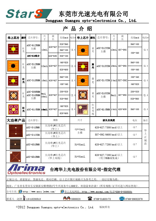
Dongguan Guangsu opto-electronics Co., Ltd.
产 品 介 绍
华上芯片 颜色 芯片型号:
尺 寸 波 长 亮度mcd 电压v
华上芯片 颜色 芯片型号:
尺 寸
波 长
亮度mcd 360-400
电压v
320-360 AOC-612RMM 620-627 红 主推 12miL 360-400 <2.4 光
<2.4
大功率产品
芯片型号:
规格
波长及亮度
电压
<2.7
备注
AOC-541RMM AOC-541YSM
大功率1W红光芯片 (华上) 大功率1W黄光芯片 (华上) 大功率1W红光芯片 (华上) 大功率1W红光芯片 (华上双线)
41*41miL 主推
620-627/7800(mcd)以上 587-592/6600(mcd)以上
公司主页: / 华上光电网址:/电话+886-3-3803801
联系人 :赵凯
13410238513
3500023
0769-81603478 版权所有
0769-89032879
©2012 Dongguan Guangsu.opto-electronics Co., Ltd.
AOC-S09RMM 主推
<2.4
320-360 460-520 <2.4 520-600
黄 光
AOC-S10YSM 9miL 587-592 主推
<2.4
320-360
红 AOC-614RMM 14miL 620-627 光
红 光 双 线 尺寸
AOC-H14RMM 14miL 620-630
电源芯片大全

LM350K LM350T LM385-1.2 LM385-2.5 LM399H LM431ACZ LM723 MC1403 MC34063 SG3524 TL431 TL494 TL497 TL7705 LT1963AEQ-3.3 SP6205-3.3
3.3V电源 TPS60500
1.2V电源 SPX3819-1.2 1.2V电源
稳压器
1A
LM1575HVT-12 12V简易开关电源
稳压器
1A
LM1575HVT-15 15V简易开关电源
稳压器
1A
LM1575HVT-ADJ 简易开关电源稳
100mA 1A
L7805,LM340T5 LM7806 6V
LM7808 8V
LM7809 9V
LM7812 12V
1A L7806
1A L7808
1A L7809
1A
L7812,LM340T12
LM7815 15V
1A
L7815,LM340T15 LM7818 18V
1A L7815
LM7824 24V
LM7905 -5V
LM7906 -6V
LM7908 -8V
LM7909 -9V
LM7912 -12V
LM7915 -15V
LM7918 -18V
LM7924 -24V
78L05 5V 100mA 78L06 6V 100mA 78L08 8V 100ma 78L09 9V 100ma 78L12 12V
5.0V
LM385-1.2 精密基准电压源
1.2V
LM385-2.5 精密基准电压源
2.5V
LM399H 6.9999V精密基准电压源
光电耦合器、运放、稳压器等元器件性能说明
524 PWM解调调制器
NE567 音调译码器 SG3525 PWM解调调制器
NE592 视频放大器 20106 前置放大器
PC817 单光耦 OP37 超低噪声精密运放
H11A2 晶体管输出 TL
H11D1 高压晶体管输出 TL062 低功耗JEFT输入双运放
MOC3020 可控硅驱动输出 LM348N 四741运放
MOC3021 可控硅驱动输出 LM358N 低功耗双运放
MOC3023 可控硅驱动输出 LM361N 高速差动比较器
6N137 高速光耦晶体管输出 LM337T 基准电压电路1A
6N138 达林顿输出 LM338K 可调三端稳压器5A
6N139 达林顿输出 LM339N 四比较器
4N25 晶体管输出 LM24J 四运放(军用级)
4N25MC 晶体管输出 LM148J 通用四运放
4N26 晶体管输出 LM1875T 无线电控制/接收器
4N30 达林顿输出 LM2904N 四运放
4N31 达林顿输出 LM301AN 通用运算放大器
4N32 达林顿输出 LM308N 单比较器
MC14433 3位半A/D转换器 ICL7135 ADC/LCD驱动BCD输出
MC14489 多字符LED显示驱动器 ICL7136 3位半CMOSADC/LCD驱动
MC145026 编码器 ICL7218 CMOS低功耗运算放大器
TLP521-2 双光耦 LM741J 单运放
TLP521-4 四光耦 LM741CN 双运放
TLP621 四光耦
TIL113 达林顿输出 OP
NE5534 双运放 UC3845 PWM电流型控制器
LM2501SL资料
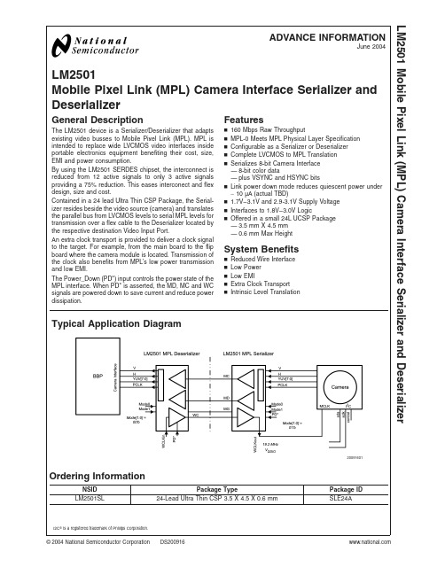
LM2501Mobile Pixel Link (MPL)Camera Interface Serializer and DeserializerGeneral DescriptionThe LM2501device is a Serializer/Deserializer that adapts existing video busses to Mobile Pixel Link (MPL).MPL is intended to replace wide LVCMOS video interfaces inside portable electronics equipment benefiting their cost,size,EMI and power consumption.By using the LM2501SERDES chipset,the interconnect is reduced from 12active signals to only 3active signals providing a 75%reduction.This eases interconect and flex design,size and cost.Contained in a 24lead Ultra Thin CSP Package,the Serial-izer resides beside the video source (camera)and translates the parallel bus from LVCMOS levels to serial MPL levels for transmission over a flex cable to the Deserializer located by the respective destination Video Input Port.An extra clock transport is provided to deliver a clock signal to the target.For example,from the main board to the flip board where the camera module is located.Transmission of the clock also benefits from MPL’s low power transmission and low EMI.The Power_Down (PD*)input controls the power state of the MPL interface.When PD*is asserted,the MD,MC and WC signals are powered down to save current and reduce power dissipation.Featuresn 160Mbps Raw Throughputn MPL-0Meets MPL Physical Layer Specification n Configurable as a Serializer or Deserializer n Complete LVCMOS to MPL Translation nSerializes 8-bit Camera Interface —8-bit color data—plus VSYNC and HSYNC bitsn Link power down mode reduces quiescent power under ∼10µA (actual TBD)n 1.7V–3.1V and 2.9-3.1V Supply Voltage n Interfaces to 1.8V–3.0V LogicnOffered in a small 24L UCSP Package —3.5mm X 4.5mm —0.6mm Max HeightSystem Benefitsn Reduced Wire Interface n Low Power n Low EMIn Extra Clock Transport nIntrinsic Level TranslationTypical Application Diagram20091601Ordering InformationNSID Package TypePackage ID LM2501SL24-Lead Ultra Thin CSP 3.5X 4.5X 0.6mmSLE24AI2C ®is a registered trademark of Phillips Corporation.ADVANCE INFORMATIONJune 2004LM2501Mobile Pixel Link (MPL)Camera Interface Serializer and Deserializer©2004National Semiconductor Corporation Connection Diagram20091612TOP VIEWGeneral Block Diagrams:Serializer and Deserializer20091613L M 2501 2Pin DescriptionPin NameNo.of PinsI/O,Type DescriptionMPL SERIAL BUS PINSMD1IO,MPL MPL Data line.Serializer is a Line Driver.Deserializer is a Receiver.Configured bythe Mode[1:0]pins.MC1IO,MPL MPL Clock line.Serializer is a Line Driver.Deserializer is a Receiver.Configured bythe Mode[1:0]pins.MG1Ground See VSSA below.CONFIGURATION/PARALLEL BUS PINSMode[1:0]2I,LVCMOS Mode Configuration Input pins:Mode[1:0],NOTE-Applies to REV F/G Samples only.00:Deserializer01:Serializer with PD*input10:Reserved11:ReservedPD*1I,LVCMOS Power_Down.Input pin.Active Low.When PD*is Low the device is in the sleepstate.D0–D78IO,LVCMOS8-bit Bi-directional Data Bus–Serializer Input,Deserializer OutputVS1IO,LVCMOS VSYNC–Serializer Input,Deserializer OutputHS1IO,LVCMOS HSYNC–Serializer Input,Deserializer OutputPCLK1IO,LVCMOS Pixel Clock.Serializer Input,Deserializer OutputWHISPER CLOCKWCLKIO1IO,LVCMOS Extra Clock Input for WhisperClock Link–Deserializer Input.Serializer Output.WC1IO,MPL Extra WhisperClock MPL signal–Serializer is an MPL input signal,Deserializer isan MPL output signal.POWER/GROUND PINSV DDA1Power Power Supply Pin for the MPL Interface.3.0V±3%V SSA1Ground Ground Pin for the MPL Interface,also known as MG(MPL Ground)V DD1Power Power Supply Pin for the digital core and Serializer PLL.3.0V±3%V SS1Ground Ground Pin for the digital core and Serializer PLL.V DDIO1Power Power Supply Pin for the parallel interface.1.7V to3.1VV SSIO1Ground Ground Pin for the parallel interface.Notes:I=Input,O=Output,IO=Input/OutputDo NOT float unused inputs.ES Revision notesRev D/E Sampled on MPL200EVK Use prior datasheet editionRev F S/D*and TM pins changed to Mode[1:0]Use this datasheet editionRev G MPL RX enhancementsLM25013Absolute Maximum Ratings (Note 1)If Military/Aerospace specified devices are required,please contact the National Semiconductor Sales Office/Distributors for availability and specifications.Supply Voltage (V DDA )−0.3V to +TBDV Supply Voltage (V DD )−0.3V to +TBDV Supply Voltage (V DDIO )−0.3V to +TBDV LVCMOS Input/Output Voltage −0.3V to (V DDIO+0.3V)MPL Input/Output Voltage TBD Junction Temperature +150˚CStorage Temperature −65˚C to +150˚CLead Temperature Soldering,4Seconds +260˚CESD Ratings:HBM,1.5k Ω,100pF≥±2kVEIAJ,0Ω,200pF ≥±200V Maximum Package Power Dissipation Capacity at 25˚C24L UCSP PackageTBD W Derate TBD Package above 25˚CTBD mW/˚CRecommended Operating ConditionsMin Typ MaxUnitsSupply Voltage V DDA to V SSA and V DD to V SS 2.9 3.03.1V V DDIO to V SSIO 1.7 3.1V PLK Clock Frequency 416MHz WC Clock Frequency 428MHz Ambient Temperature2570˚C Electrical CharacteristicsOver recommended operating supply and temperature ranges unless otherwise specified.(Note 2)Symbol ParameterConditionsMinTypMaxUnitsMPL I OLL Logic Low Current 4.8I B5.0I B 5.3I BµA I OMS Mid Scale Current 3.0I B µA I OHL Logic High Current 0.8I B 1.0I B 1.2I B µA I B Current Bias150µALVCMOS (1.7V to 3.1V)V IH Input Voltage High Level 0.7V DDIOV DDIO +0.3V V IL Input Voltage Low Level −0.30.3V DDIOV I IN Input Current (includes I OZ )−50+5µA I IH Input Current High Level −10+1µA I IL Input Current Low Level −10+1µA V OH Output Voltage High Level I OH =−2mA 0.8V DDIOV V OL Output Voltage Low Level I OL =2mA 0.2V DDIO V I OSOutput Short Circuit CurrentV OUT =0VTBDmASUPPLY CURRENT I CCTotal SupplyCurrent —EnabledPCLK =16MHz WC =28MHz MD =0101-1010pattern C L =15pFSerializerTBDTBDµADeserializerTBD TBD µA I CCZSupply Current —Disable Power_Down Mode PD*=L110µA PD*=L110µAL M 2501 4Switching CharacteristicsOver recommended operating supply and temperature ranges unless otherwise specified.(Note2)Symbol Parameter Conditions Min Typ Max Units PARALLEL BUS TIMINGt SET Set Time-Data to Clock Inputs Figure2TBD ns t HOLD Hold Time-Clock to Data TBD nst RISE Rise Time Outputs,C L=15pF nst FALL Fall Time ns PC LOW PCLK Low50% PC HIGH PCLK High50% t DVBC Data Valid before Clock Figure2TBD ns t DVAC Data Valid after Clock TBD ns SERIAL BUS TIMINGt DVBC Figure1t DVACPOWER UP TIMING(see Figures5,6)t1WC Start Up Delay Figure5Planned Rev G ES test Chip willdouble WC cyc counts on T1to T4(SER)parameters to support higherWC rates.100WC CYCt2WC Low Initialization LowState111213WC CYC t3WC Pulse Width High111213WC CYC t4WC Low State111213WC CYC t5WC IN to WC OUT Latency(SER)678WC CYC t6TBD9WC CYC t7SER PLL Lock Time Figure64,096MC CYC t8MC Low Initialization LowState111213MC CYC t9MC Pulse Width High111213MC CYC t10MC Low State111213MC CYC t11SER Latency TBD MC CYC t12DES Latency TBD MC CYC POWER OFF TIMINGt PAZ Disable Time to Power Offµst PZA Enable Time from PowerOffµsLM25015Input Timing RequirementsOver recommended operating supply and temperature ranges unless otherwise specified.(Note 2)Symbol ParameterConditionsMin TypMax Units REFERENCE CLOCK (WCLK IN )f WC Clock Frequency 428MHz WC DC Clock Duty Cycle 455055%t TClock Transition Times (Rise or Fall,10%–90%)16nsPIXEL CLOCK (PCLK)f PCLK Clock Frequency 416MHz t CP Clock Period 62.5250ns CLK DC Clock Duty Cycle 455055%t TClock transition Time16nsNote 1:“Absolute Maximum Ratings“are those values beyond which the safety of the device cannot be guaranteed.They are not meant to imply that the device should be operated at these limits.The tables of “Electrical Characteristics”specify conditions for device operation.Note 2:Typical values are given for V DD =V DDA =3.0V and V DDIO =2.7V and T A =25˚C.Note 3:Current into a device pin is defined as positive.Current out of device pins is defined as negative.Voltages are referenced to Ground unless otherwise specified.Timing Diagrams20091610FIGURE 1.Serial Data Valid20091611FIGURE 2.Parallel Set,Hold and Data ValidL M 2501 6Application InformationTypical application connections for the LM2501are shown below.The application shown in Figure 3illustrates a connection between an Image sensor and a host utilizing an MPL-0link..20091614FIGURE 3.Camera ApplicationLM25017Functional DescriptionSERIAL BUS OPERATION Bus OverviewThe MPL bus is a simple 2-signal line interface that is intended to replace wide low voltage CMOS video busses inside handheld portable devices.The MPL physical layer is purpose-built for an extremely low power and low EMI data transmission while requiring the fewest number of signal lines.No external line components are required,as termina-tion is provided internal to the MPL receiver.The MPL inter-face is designed to be used with common 50Ωlines using standard materials and connectors.Lines may be microstrip or stripline construction.Total length of the interconnect is expected to be less than 0.3meters.This device is meets the requirements of the MPL-0Standard (PHY Layer only).SERIAL BUS TIMINGData valid is relative to both edges as shown in Figure 4.Data valid is specified as:Data Valid before Clock,Data Valid after Clock,(Note relative to both edges).SERIAL BUS PHASESThere are three bus phases on the MPL serial bus.These are determined by the state of the MC and MD lines.Two of the bus phases have options.The MPL bus phases are shown in Table 1.TABLE 1.MPL Bus PhasesNameWC StateMC StateMD StatePhase Description Pre-PhasePost-Phase OFF (O)000Bus is Powered-Off na I (WC)Initialization (I)WC A 00WC Start Up O I (MC)MC/MDA A 0MPL Start Up I (WC)A Active (A)AAXData Out (Write)I (MC)A or ONotes on Line State:0=no current (off),L =Logic Low,H =Logic High,X =Low or High,A —Active Clock20091602FIGURE 4.Master-to-Slave Timing (MC,MDm)L M 2501 8Functional Description(Continued)SERIAL BUS POWER-UPIn the sleep state,WC,MC and MD are turned off with zero current flowing.Both devices need to be enabled by assert-ing their PD*inputs.The DES will then initialize the SER via the WC signal as shown in Figure5.The DES waits7WC cycles before its WCLK out is active.Note,there is no phase or frequency relationship between WC and MC.20091603FIGURE5.Bus Power Up Timing—WCLM25019Functional Description(Continued)In Figure 6,the Serializer timing is shown.For the part to establish lock,WCLKIO(out)must be active,and a valid PCLK applied.After lock is obtained,the MC and MD lines are initialized and then active transmission occurs.Table Switching Characteristics lists the timing parameters of Fig-ures 5,6.SERIAL BUS POWER-OFFIn the power-off state,WC,MD and MC are turned off with zero current flowing.This is considered the Sleep state (Power-off)and the transition off may occur after the last data bit time or at any time afterwards from an Idle phase as shown in Figure 7.20091604FIGURE 6.Bus Power Up Timing —MC/MD20091605FIGURE 7.Bus Power Down TimingL M 2501 10Functional Description(Continued)CAMERA INTERFACEThe Camera Interface provides serialization of color and control bits.The interface provides data transport in a single direction.Byte alignment is provided by the intrinsic firstrising edge of the MC line.PCLK is required and must be free-running .Data may be raw Bayer or BT656color infor-mation.Data is strobed on the rising-edge on the input to the Serializer.Data is sent LSB first (D0).MPL provides the data transport path,control of the Camera device is provided by an I 2C control bus.20091606FIGURE 8.Camera Mode Serial Interface20091607FIGURE 9.Parallel Bus TimingLM250111Features and OperationPOWER DOWN/OFFThe device may be powered by its PD*pin.A Low on this pin will power down the entire device.TABLE 2.Power Down Output StatesMode Pin Type Output State in Power DownSER WCLKIO LVCMOS LOW SER MC MPL OFF SER MD MPL OFF DES D[0:7]LVCMOS LOW DES V,H LVCMOS LOW DES PCLK LVCMOS LOW DESWCMPLOFFUN-USED/OPEN INPUTSUn-used control/inputs pins must be driven to their appropri-ate logic states to set up the desired operating modes.UN-USED OUTPUTSUnused outputs should be left open to minimize power dis-sipation.POWERING UPThe LM2501should be powered up with all power supplies at the same time,alternately VDDIO may lag VDD and VDDA.Do not power up with VDDIO before VDD and VDDA.PHASE-LOCKED LOOPWhen the device is configured as a Serializer,a PLL is provided to generate the serial link clock.The Phase-locked loop system generates the serial data clock at five times the input clock.The PLL operates with an input clock between 4MHz and 16MHz.The Deserializer does not utilize the PLL and its PLL is powered down.RESETPD*should be held Low until the power supply has powered up and is stable.The PD*should then be de-asserted to generate a RESET and start up.Stopping the WCLKIO or the PCLK will not RESET the part.A power cycle or PD*cycle is requested to generate a RESET event.SERIALIZER/DESERIALIZER SELECTIONThe Mode[1:0]pins are used to configure the device as either a Serializer or Deserializer and other configuration options.WHISPERCLOCKAn additional clock signal is sent from the Deserializer to the Serializer.This can be used to pass a clock reference (4MHz to 28MHz)up to the Camera device from the host.This link is independent of the Serial data path (opposite direction).See also Figure 5.The SER can only start up,if the WCLKIO(ser-out)has been active.20091608FIGURE 10.Sleep to ActiveL M 2501 12Features and Operation(Continued) When the Deserializer’s PD*signal is de-asserted,the WC output will power up and initialize the serializer and start transmitting the clock reference.Once the Serializer re-ceived the clock,it waits seven cycles,and then outputs the clock signal.Seven cycles later,the Serializer’s PLL will begin to lock if PCLK is present.When the Deserializer’s PD*signal is asserted,the WC signal is turned off.MISC.Definitions:Bus States:Logic Low—5Idata flowing from the Receiver to theDriverLogic High—Idata flowing from the Receiver to the Driver Power Off—No Current flowing in the interconnect Signals&Nomenclature:MD=MPL Data Signal,subscript denotes source,m= master,s=slaveMC=MPL Clock SignalWC=MPL WhisperClock Signal*=Active Low Signal20091609FIGURE11.Active to SleepLM2501 13Physical Dimensionsinches (millimeters)unless otherwise notedOrder Number LM2501SL NS Package Number SLE24ALIFE SUPPORT POLICYNATIONAL’S PRODUCTS ARE NOT AUTHORIZED FOR USE AS CRITICAL COMPONENTS IN LIFE SUPPORT DEVICES OR SYSTEMS WITHOUT THE EXPRESS WRITTEN APPROVAL OF THE PRESIDENT AND GENERAL COUNSEL OF NATIONAL SEMICONDUCTOR CORPORATION.As used herein:1.Life support devices or systems are devices or systems which,(a)are intended for surgical implant into the body,or (b)support or sustain life,and whose failure to perform when properly used in accordance with instructions for use provided in the labeling,can be reasonably expected to result in a significant injury to the user. 2.A critical component is any component of a life support device or system whose failure to perform can be reasonably expected to cause the failure of the life support device or system,or to affect its safety or effectiveness.BANNED SUBSTANCE COMPLIANCENational Semiconductor certifies that the products and packing materials meet the provisions of the Customer Products Stewardship Specification (CSP-9-111C2)and the Banned Substances and Materials of Interest Specification (CSP-9-111S2)and contain no ‘‘Banned Substances’’as defined in CSP-9-111S2.National Semiconductor Americas Customer Support CenterEmail:new.feedback@ Tel:1-800-272-9959National SemiconductorEurope Customer Support CenterFax:+49(0)180-5308586Email:europe.support@Deutsch Tel:+49(0)6995086208English Tel:+44(0)8702402171Français Tel:+33(0)141918790National Semiconductor Asia Pacific Customer Support CenterEmail:ap.support@National SemiconductorJapan Customer Support Center Fax:81-3-5639-7507Email:jpn.feedback@ Tel:81-3-5639-7560L M 2501M o b i l e P i x e l L i n k (M P L )C a m e r a I n t e r f a c e S e r i a l i z e r a n d D e s e r i a l i z e rNational does not assume any responsibility for use of any circuitry described,no circuit patent licenses are implied and National reserves the right at any time without notice to change said circuitry and specifications.。
- 1、下载文档前请自行甄别文档内容的完整性,平台不提供额外的编辑、内容补充、找答案等附加服务。
- 2、"仅部分预览"的文档,不可在线预览部分如存在完整性等问题,可反馈申请退款(可完整预览的文档不适用该条件!)。
- 3、如文档侵犯您的权益,请联系客服反馈,我们会尽快为您处理(人工客服工作时间:9:00-18:30)。
LM25017 SNVS951–DECEMBER2012 LM2501748V,650mA Constant On-Time Synchronous Buck RegulatorCheck for Samples:LM25017FEATURES•Frequency Adjustable to1MHz•Adjustable Undervoltage Lockout(UVLO)•Integrated48V,High and Low Side Switches•Remote Shutdown•No Schottky Required•Thermal Shutdown•Constant On-time Control•No Loop Compensation RequiredAPPLICATIONS•Ultra-Fast Transient Response•Industrial Equipments•Nearly Constant Operating Frequency•Smart Power Meters•Intelligent Peak Current Limit•Telecommunication Systems•Adjustable Output Voltage from1.225V•Isolated Bias Supply•Precision2%Feedback ReferenceDESCRIPTIONThe LM25017is a48V,650mA synchronous step-down regulator with integrated high side and low side MOSFETs.The constant-on-time(COT)control scheme employed in the LM25017requires no loop compensation,provides excellent transient response,and enables very low step-down ratios.The on-time varies inversely with the input voltage resulting in nearly constant frequency over the input voltage range.A high voltage startup regulator provides bias power for internal operation of the IC and for integrated gate drivers.A peak current limit circuit protects against overload conditions.The undervoltage lockout(UVLO)circuit allows the input undervoltage threshold and hysteresis to be independently programmed.Other protection features include thermal shutdown and bias supply undervoltage lockout(V CC UVLO).The LM25017is available in LLP-8and PSOP-8plastic packages.Packages•LLP-8•PSOP-8Typical ApplicationPlease be aware that an important notice concerning availability,standard warranty,and use in critical applications ofTexas Instruments semiconductor products and disclaimers thereto appears at the end of this data sheet.All trademarks are the property of their respective owners.PRODUCTION DATA information is current as of publication date.Copyright©2012,Texas Instruments Incorporated Products conform to specifications per the terms of the TexasInstruments standard warranty.Production processing does notnecessarily include testing of all parameters.UVLO 3RON4RTN 1VIN 28 SW7 BST6 VCC5 FBPSOP-8Exp PadLM25017SNVS951–DECEMBER 2012Connection DiagramFigure 1.Top View (Connect Exposed Pad to RTN)Figure 2.Top View (Connect Exposed Pad to RTN)Pin FunctionsTable 1.Pin DescriptionsPin Name DescriptionApplication Information1RTN Ground Ground connection of the integrated circuit.2V IN Input VoltageOperating input range is 9V to 48V.3UVLOInput Pin of Undervoltage ComparatorResistor divider from V IN to UVLO to GND programs the undervoltage detection threshold.An internal current source is enabled when UVLO is above 1.225V to provide hysteresis.When UVLO pin is pulled below 0.66V externally,the parts goes in shutdown mode.4R ONOn-Time ControlA resistor between this pin and V IN sets the switch on-time as a function of V IN .Minimum recommended on-time is 100ns at max input voltage.5FB FeedbackThis pin is connected to the inverting input of the internal regulation comparator.The regulation level is 1.225V.6V CCOutput from the Internal High Voltage Series Pass The internal V CC regulator provides bias supply for the Regulator.Regulated at 7.6V gate drivers and other internal circuitry.A 1.0μF decoupling capacitor is recommended.7BSTBootstrap CapacitorAn external capacitor is required between the BST and SW pins (0.01μF ceramic).The BST pin capacitor is charged by the V CC regulator through an internal diode when the SW pin is low.8SW Switching Node Power switching node.Connect to the output inductor and bootstrap capacitor.EPExposed PadExposed pad must be connected to RTN pin.Connect to system ground plane on application board for reduced thermal resistance.These devices have limited built-in ESD protection.The leads should be shorted together or the device placed in conductive foam during storage or handling to prevent electrostatic damage to the MOS gates.2Submit Documentation FeedbackCopyright ©2012,Texas Instruments IncorporatedProduct Folder Links:LM25017LM25017 SNVS951–DECEMBER2012Absolute Maximum Ratings(1)V IN,UVLO to RTN-0.3V to53VSW to RTN-1.5V to V IN+0.3VBST to V CC53VBST to SW13VR ON to RTN-0.3V to53VV CC to RTN-0.3V to13VFB to RTN-0.3V to5VESD Rating(Human Body Model(2)2kVLead Temperature(3)200°CStorage Temperature Range-55°C to+150°C(1)Absolute Maximum Ratings are limits beyond which damage to the device may occur.Operating Ratings are conditions under whichoperation of the device is intended to be functional.For specifications and test conditions,see the Electrical Characteristics.The RTN pin is the GND reference electrically connected to the substrate.(2)The human body model is a100pF capacitor discharged through a1.5kΩresistor into each pin.(3)For detailed information on soldering plastic PSOP package,refer to the Packaging Data Book available from National SemiconductorCorporation.Max solder time not to exceed4seconds.Operating Ratings(1)V IN Voltage9V to48V Operating Junction Temperature−40°C to+125°C (1)Absolute Maximum Ratings are limits beyond which damage to the device may occur.Operating Ratings are conditions under whichoperation of the device is intended to be functional.For specifications and test conditions,see the Electrical Characteristics.The RTN pin is the GND reference electrically connected to the substrate.Copyright©2012,Texas Instruments Incorporated Submit Documentation Feedback3Product Folder Links:LM25017LM25017SNVS951–Electrical CharacteristicsSpecifications with standard typeface are for T J=25°C,and those with boldface type apply over full Operating Junction Temperature range.V IN=48V,unless otherwise stated.See(1).Symbol Parameter Conditions Min Typ Max UnitsV CC SupplyV CC Reg V CC Regulator Output V IN=48V,I CC=20mA 6.257.68.55V V CC Current Limit V IN=48V(2)26mAV CC Undervoltage Lockout Voltage 4.15 4.5 4.9V(V CC increasing)V CC Undervoltage Hysteresis300mVV CC Drop Out Voltage V IN=9V,I CC=20mA 2.3VI IN Operating Current Non-Switching,FB=3V 1.75mAI IN Shutdown Current UVLO=0V50225µA Switch CharacteristicsBuck Switch R DS(ON)I TEST=200mA,BST-SW=0.8 1.8Ω7VSynchronous R DS(ON)I TEST=200mA0.451ΩGate Drive UVLO V BST−V SW Rising 2.43 3.6VGate Drive UVLO Hysteresis260mV Current LimitCurrent Limit Threshold0.7 1.02 1.3ACurrent Limit Response Time Time to Switch Off150nsOFF-Time Generator(Test1)FB=0.1V,V IN=48V12µsOFF-Time Generator(Test2)FB=1.0V,V IN=48V 2.5µsOn-Time GeneratorT ON Test1V IN=32V,R ON=100k270350460nsT ON Test2V IN=48V,R ON=100k188250336nsT ON Test4V IN=10V,R ON=250k188032004425ns Minimum Off-TimeMinimum Off-Timer FB=0V144ns Regulation and Overvoltage ComparatorsFB Regulation Level Internal Reference Trip Point 1.2 1.225 1.25Vfor Switch ONFB Overvoltage Threshold Trip Point for Switch OFF 1.62VFB Bias Current60nA Undervoltage Sensing FunctionUV Threshold UV Rising 1.19 1.225 1.26VUV Hysteresis Input Current UV=2.5V-10-20-29µARemote Shutdown Threshold Voltage at UVLO Falling0.320.66VRemote Shutdown Hysteresis110mV Thermal ShutdownTsd Thermal Shutdown Temperature165°C Thermal Shutdown Hysteresis20°C Thermal ResistanceJunction to Ambient PSOP-840°C/WθJALLP-840°C/W(1)All electrical characteristics having room temperature limits are tested during production at T A=25°C.All hot and cold limits arespecified by correlating the electrical characteristics to process and temperature variations and applying statistical process control. (2)V CC provides self bias for the internal gate drive and control circuits.Device thermal limitations limit external loading.4Submit Documentation Feedback Copyright©2012,Texas Instruments IncorporatedProduct Folder Links:LM25017LM25017 SNVS951–DECEMBER2012Typical Performance CharacteristicsFigure4.V CC vs V INFigure5.V CC vs I CCCopyright©2012,Texas Instruments Incorporated Submit Documentation Feedback5Product Folder Links:LM25017LM25017SNVS951– Typical Performance Characteristics(continued)Figure7.T ON vs V IN and R ONFigure8.T OFF(I LIM)vs V FB and V IN6Submit Documentation Feedback Copyright©2012,Texas Instruments IncorporatedProduct Folder Links:LM25017LM25017 SNVS951–DECEMBER2012 Typical Performance Characteristics(continued)Figure9.I IN vs V IN(Operating,Non Switching)Figure10.I IN vs V IN(Shutdown)Figure11.Switching Frequency vs V INCopyright©2012,Texas Instruments Incorporated Submit Documentation Feedback7Product Folder Links:LM25017FBV INV CCSWRTNBSTR LM25017SNVS951–DECEMBER 2012Block DiagramFigure 12.Functional Block DiagramFunctional DescriptionThe LM25017step-down switching regulator features all the functions needed to implement a low cost,efficient,buck converter capable of supplying up to 650mA to the load.This high voltage regulator contains 48V,N-channel buck and synchronous switches,is easy to implement,and is provided in thermally enhanced PSOP-8and LLP-8packages.The regulator operation is based on a constant on-time control scheme using an on-time inversely proportional to V IN .This control scheme does not require loop compensation.The current limit is implemented with a forced off-time inversely proportional to V OUT .This scheme ensures short circuit protection while providing minimum foldback.The simplified block diagram of the LM25017is shown in ,Functional Block Diagram.The LM25017can be applied in numerous applications to efficiently regulate down higher voltages.This regulator is well suited for 12V and 24V rails.Protection features include:thermal shutdown,Undervoltage Lockout (UVLO),minimum forced off-time,and an intelligent current limit.Control OverviewThe LM25017buck regulator employs a control principle based on a comparator and a one-shot on-timer,with the output voltage feedback (FB)compared to an internal reference (1.225V).If the FB voltage is below the reference the internal buck switch is turned on for the one-shot timer period,which is a function of the input voltage and the programming resistor (R ON ).Following the on-time the switch remains off until the FB voltage falls below the reference,but never before the minimum off-time forced by the minimum off-time one-shot timer.When the FB pin voltage falls below the reference and the minimum off-time one-shot period expires,the buck switch is turned on for another on-time one-shot period.This will continue until regulation is achieved and the FB voltage is approximately equal to 1.225V (typ).8Submit Documentation FeedbackCopyright ©2012,Texas Instruments IncorporatedProduct Folder Links:LM25017VOUTVOUT(low ripple)VOUTVOUT (low ripple)R FB2 + R FB1V OUT = 1.225V xR FB1V OUT g sw =10-10x R ONLM25017SNVS951–DECEMBER 2012In a synchronous buck converter,the low side (sync)FET is ‘on’when the high side (buck)FET is ‘off’.The inductor current ramps up when the high side switch is ‘on’and ramps down when the high side switch is ‘off’.There is no diode emulation feature in this IC,and therefore,the inductor current may ramp in the negative direction at light load.This causes the converter to operate in continuous conduction mode (CCM)regardless of the output loading.The operating frequency remains relatively constant with load and line variations.The operating frequency can be calculated as follows:(1)The output voltage (V OUT )is set by two external resistors (R FB1,R FB2).The regulated output voltage is calculated as follows:(2)(3)This regulator regulates the output voltage based on ripple voltage at the feedback input,requiring a minimum amount of ESR for the output capacitor (C OUT ).A minimum of 25mV of ripple voltage at the feedback pin (FB)is required for the LM25017.In cases where the capacitor ESR is too small,additional series resistance may be required (R C in Figure 13Low Ripple Output Configuration).For applications where lower output voltage ripple is required the output can be taken directly from a low ESR output capacitor,as shown in Figure 13Low Ripple Output Configuration.However,R C slightly degrades the load regulation.V CC RegulatorThe LM25017contains an internal high voltage linear regulator with a nominal output of 7.6V.The input pin (V IN )can be connected directly to the line voltages up to 48V.The V CC regulator is internally current limited to 30mA.The regulator sources current into the external capacitor at V CC .This regulator supplies current to internal circuit blocks including the synchronous MOSFET driver and the logic circuits.When the voltage on the V CC pin reaches the undervoltage lockout (V CC UVLO)threshold of 4.5V,the IC is enabled.The V CC regulator contains an internal diode connection to the BST pin to replenish the charge in the gate drive boot capacitor when SW pin is low.At high input voltages,the power dissipated in the high voltage regulator is significant and can limit the overall achievable output power.As an example,with the input at 48V and switching at high frequency,the V CC regulator may supply up to 7mA of current resulting in 48V x 7mA =336mW of power dissipation.If the V CC voltage is driven externally by an alternate voltage source,between 8V and 13V,the internal regulator is disabled.This reduces the power dissipation in the IC.Figure 13.Low Ripple Output ConfigurationCopyright ©2012,Texas Instruments Incorporated Submit Documentation Feedback9Product Folder Links:LM250170.07 x V INT OFF(ILIM) =V FB + 0.2VP s10-10 x R ONT ON =V INLM25017SNVS951–DECEMBER 2012Regulation ComparatorThe feedback voltage at FB is compared to an internal 1.225V reference.In normal operation,when the output voltage is in regulation,an on-time period is initiated when the voltage at FB falls below 1.225V.The high side switch will stay on for the on-time,causing the FB voltage to rise above 1.225V.After the on-time period,the high side switch will stay off until the FB voltage again falls below 1.225V.During start-up,the FB voltage will be below 1.225V at the end of each on-time,causing the high side switch to turn on immediately after the minimum forced off-time of 144ns.The high side switch can be turned off before the on-time is over,if the peak current in the inductor reaches the current limit threshold.Overvoltage ComparatorThe feedback voltage at FB is compared to an internal 1.62V reference.If the voltage at FB rises above 1.62V the on-time pulse is immediately terminated.This condition can occur if the input voltage and/or the output load changes suddenly.The high side switch will not turn on again until the voltage at FB falls below 1.225V.On-Time GeneratorThe on-time for the LM25017is determined by the R ON resistor,and is inversely proportional to the input voltage (V IN ),resulting in a nearly constant frequency as V IN is varied over its range.The on-time equation for the LM25017is:(4)See figure “T ON vs V IN and R ON ”in the section “Performance Curves”.R ON should be selected for a minimum on-time (at maximum V IN )greater than 100ns,for proper operation.This requirement limits the maximum switching frequency for high V IN .Current LimitThe LM25017contains an intelligent current limit off-timer.If the current in the buck switch exceeds 1.02A the present cycle is immediately terminated,and a non-resetable off-timer is initiated.The length of off-time is controlled by the FB voltage and the input voltage V IN .As an example,when FB =0V and V IN =48V,the maximum off-time is set to 16μs.This condition occurs when the output is shorted,and during the initial part of start-up.This amount of time ensures safe short circuit operation up to the maximum input voltage of 48V.In cases of overload where the FB voltage is above zero volts (not a short circuit)the current limit off-time is reduced.Reducing the off-time during less severe overloads reduces the amount of foldback,recovery time,and start-up time.The off-time is calculated from the following equation:(5)The current limit protection feature is peak limited.The maximum average output will be less than the peak.N-Channel Buck Switch and DriverThe LM25017integrates an N-Channel Buck switch and associated floating high voltage gate driver.The gate driver circuit works in conjunction with an external bootstrap capacitor and an internal high voltage diode.A 0.01uF ceramic capacitor connected between the BST pin and the SW pin provides the voltage to the driver during the on-time.During each off-time,the SW pin is at approximately 0V,and the bootstrap capacitor charges from V CC through the internal diode.The minimum off-timer,set to 144ns ,ensures a minimum time each cycle to recharge the bootstrap capacitor.Synchronous RectifierThe LM25017provides an internal synchronous N-Channel MOSFET rectifier.This MOSFET provides a path for the inductor current to flow when the high-side MOSFET is turned off.The synchronous rectifier has no diode emulation mode,and is designed to keep the regulator in continuous conduction mode even during light loads which would otherwise result in discontinuous operation.10Submit Documentation FeedbackCopyright ©2012,Texas Instruments IncorporatedProduct Folder Links:LM25017LM25017 SNVS951–DECEMBER2012Undervoltage DetectorThe LM25017contains a dual level undervoltage lockout(UVLO)circuit.When the UVLO pin voltage is below 0.66V,the controller is in a low current shutdown mode.When the UVLO pin voltage is greater than0.66V but less than1.225V,the controller is in standby mode.In standby mode the V CC bias regulator is active while the regulator output is disabled.When the V CC pin exceeds the V CC undervoltage threshold and the UVLO pin voltage is greater than1.225V,normal operation begins.An external set-point voltage divider from V IN to GND can be used to set the minimum operating voltage of the regulator.UVLO hysteresis is accomplished with an internal20μA current source that is switched on or off into the impedance of the set-point divider.When the UVLO threshold is exceeded,the current source is activated to quickly raise the voltage at the UVLO pin.The hysteresis is equal to the value of this current times the resistance R UV2.UVLO V CC Mode Description<0.66V Shutdown V CC regulator disabled.Switcher disabled.0.66V–1.225V Standby V CC regulator enabledSwitcher disabled.>1.225V V CC<4.5V Standby V CC regulator enabled.Switcher disabled.V CC>4.5V Operating V CC enabled.Switcher enabled.If the UVLO pin is wired directly to the V IN pin,the regulator will begin operation once the V CC undervoltage is satisfied.Figure14.UVLO Resistor SettingThermal ProtectionThe LM25017should be operated so the junction temperature does not exceed150°C during normal operation. An internal Thermal Shutdown circuit is provided to protect the LM25017in the event of a higher than normal junction temperature.When activated,typically at165°C,the controller is forced into a low power reset state, disabling the buck switch and the V CC regulator.This feature prevents catastrophic failures from accidental device overheating.When the junction temperature reduces below145°C(typical hysteresis=20°C),the V CC regulator is enabled,and normal operation is resumed.Application InformationSELECTION OF EXTERNAL COMPONENTSSelection of external components is illustrated through a design example.The design example specifications are as follows:Buck Converter Design SpecificationsInput voltage range12.5V to48VOutput voltage10VMaximum Load current500mASwitching Frequency200kHzCopyright©2012,Texas Instruments Incorporated Submit Documentation Feedback11Product Folder Links:LM25017ûI LC OUT =8 x g sw x ûV rippleûI L(MAX)I LI (peak) = I OUT +2= 590 mA V IN - V OUT ûI L =L1 x g SWV OUTV IN xV OUT g SW =K x R OND MIN g SW(MAX) =T ON(MIN)10/48100 ns== 2.1 MHz1 - D MAX g SW(MAX) =T OFF(MIN)1 - 10/12.5200 ns == 1 MHzLM25017SNVS951–DECEMBER 2012RFB1,RFB2:V OUT =V FB x (R FB2/R FB1+1),and since V FB =1.225V,the ratio of R FB2to R FB1calculates as 7:1.Standard values of 6.98k Ωand 1.00k Ωare chosen.Other values could be used as long as the 7:1ratio is maintained.Frequency Selection:At the minimum input voltage,the maximum switching frequency of LM25017is restricted by the forced minimum off-time (T OFF(MIN))as given by:(6)Similarly,at maximum input voltage,the maximum switching frequency of LM25017is restricted by the minimumT ON as given by:(7)Resistor R ON sets the nominal switching frequency based on the following equations:(8)where K =1x 10⁻¹⁰.Operation at high switching frequency results in lower efficiency while providing the smallest solution.For this example a conservative 200kHz was selected,resulting in R ON =504k Ω.Selecting a standard value for R ON =499k Ωresults in a nominal frequency of 202kHz.Inductor Selection:The minimum inductance is selected to limit the output ripple to 20to 40percent of the maximum load current.In addition,the peak inductor current at maximum load should be smaller than the minimum current limit as given in electrical characteristics table.The inductor current ripple is given by:(9)The maximum ripple is observed at maximum input voltage.Substituting V IN =48V and ΔIL =40percent x I OUT(max)results in L1=197μH.The next higher standard value of 220μH is chosen.The peak-to-peak minimum and maximum inductor current ripples of 35mA and 179mA are given at minimum and maximum input voltages respectively.The peak inductor and switch current is given by(10)which is smaller than the minimum current limit.The inductor should be able to withstand the maximum current limit of 1.3A,which can be reached during startup and overload conditions.Figure 15.Reference Schematic for Selection of External ComponentsOutput Capacitor:The output capacitor is selected to minimize the capacitive ripple across it.The maximum ripple is observed at maximum input voltage and is given by:(11)12Submit Documentation FeedbackCopyright ©2012,Texas Instruments IncorporatedProduct Folder Links:LM25017R UV2V IN (UVLO,rising) = 1.225V x R UV1+ 1()V IN (HYS)=I HYS x R UV2I OUT(MAX)C IN 8 x g SW x ûV IN>25 mV R C ûI L(MIN)V OUTV REFx>LM25017SNVS951–DECEMBER 2012where ΔV ripple is the voltage ripple across the capacitor.Substituting ΔV ripple =10mV gives C OUT =12.64μF.A 22μF standard value is selected.An X5R or X7R type capacitor with a voltage rating 16V or higher should be selected.Series Ripple Resistor R C :The series resistor should be selected to produce sufficient ripple at the feedback node.The ripple produced by R C is proportional to the inductor current ripple,and therefore R C should be chosen for minimum inductor current ripple which occurs at minimum input voltage.The R C is calculated by the equation:(12)This gives an R C of greater than or equal to 5.15Ω.Selecting R C =5.23Ωresults in ~1V of maximum output voltage ripple.For applications requiring lower output voltage ripple,Type II or Type III ripple injection circuits should be used as described in the section “Ripple Configuration”.V CC and Bootstrap Capacitor:The V CC capacitor provides charge to bootstrap capacitor as well as internal circuitry and low side gate driver.The Bootstrap capacitor provides charge to high side gate driver.A good value for CV CC is 1μF.A good value for C BST is 0.01μF.Input Capacitor:Input capacitor should be large enough to limit the input voltage ripple:(13)choosing a ΔV IN =0.5V gives a minimum C IN =1.24μF.A standard value of 2.2μF is selected.The input capacitor should be rated for the maximum input voltage under all conditions.A 50V,X7R dielectric should be selected for this design.Input capacitor should be placed directly across V IN and RTN (pin 2and 1)of the IC.If it is not possible to place all of the input capacitor close to the IC,a 0.47μF capacitor should be placed near the IC to provide a bypass path for the high frequency component of the switching current.This helps limit the switching noise.UVLO Resistors:The UVLO resistors R FB1and R FB2set the UVLO threshold and hysteresis according to the following relationship:(14)and(15)where I HYS =20μA.Setting UVLO hysteresis of 2.5V and UVLO rising threshold of 12V results in R UV1=14.53k Ωand R UV2=125k Ω.Selecting standard value of R UV1=14k Ωand R UV2=125k Ωresults in UVLO thresholds and hysteresis of 12.4V and 2.5V respectively.APPLICATION CIRCUIT:12V TO 48V INPUT AND 10V,500mA OUTPUT BUCK CONVERTERThe application schematic of a buck supply is shown in Figure 16below.For output voltage (V OUT )above the maximum regulation threshold of V CC (8.55V,see electrical characteristics),the V CC pin can be connected to V OUT through a diode (D2),as shown below,for higher efficiency and lower power dissipation in the IC.Copyright ©2012,Texas Instruments Incorporated Submit Documentation Feedback13Product Folder Links:LM25017N SV OUT2 = V OUT1 xN P- V FLM25017SNVS951–DECEMBER 2012Figure 16.Final Schematic for 12V to 48V Input,and 10V,500mA Output Buck ConverterISOLATED DC-DC CONVERTER USING LM25017An isolated supply using LM25017is shown in Figure 17below.Inductor (L)in a typical buck circuit is replaced with a coupled inductor (X1).A diode (D1)is used to rectify the voltage on a secondary output.The nominal voltage at the secondary output (V OUT2)is given by:(16)where VF is the forward voltage drop of D1,and NP,NS are the number of turns on the primary and secondary of coupled inductor X1.For output voltage (V OUT1)above the maximum V CC (8.55V),the V CC pin can be diode connected to V OUT1for higher efficiency and low dissipation in the IC.See AN-2292for a complete isolated bias design.Figure 17.Typical Isolated Application SchematicRIPPLE CONFIGURATIONLM25017uses Constant-On-Time (COT)control scheme,in which the on-time is terminated by an on-timer,and the off-time is terminated by the feedback voltage (V FB )falling below the reference voltage (V REF ).Therefore,for stable operation,the feedback voltage must decrease monotonically,in phase with the inductor current during the off-time.Furthermore,this change in feedback voltage (V FB )during off-time must be large enough to suppress any noise component present at the feedback node.Table 1shows three different methods for generating appropriate voltage ripple at the feedback node.Type 1and Type 2ripple circuits couple the ripple at the output of the converter to the feedback node (FB).The output voltage ripple has two components:1.Capacitive ripple caused by the inductor current ripple charging/discharging the output capacitor.2.Resistive ripple caused by the inductor current ripple flowing through the ESR of the output capacitor.14Submit Documentation FeedbackCopyright ©2012,Texas Instruments IncorporatedProduct Folder Links:LM25017。