MAX1277AETC+T中文资料
MEMORY存储芯片MAX1771ESA+T中文规格书
ABSOLUTE MAXIMUM RATINGSSupply VoltageV+ to GND...............................................................-0.3V, 17V EXT, CS, REF, SHDN, FB to GND...................-0.3V, (V+ + 0.3V) GND to AGND.............................................................0.1V, -0.1V Continuous Power Dissipation (T A= +70°C)Plastic DIP (derate 9.09mW/°C above +70°C)............727mW SO (derate 5.88mW/°C above +70°C).........................471mW CERDIP (derate 8.00mW/°C above +70°C).................640mW Operating Temperature RangesMAX1771C_A.....................................................0°C to +70°C MAX1771E_A..................................................-40°C to +85°C MAX1771MJA................................................-55°C to +125°C Junction TemperaturesMAX1771C_A/E_A.......................................................+150°C MAX1771MJA..............................................................+175°C Storage Temperature Range.............................-65°C to +160°C Lead Temperature (soldering, 10sec).............................+300°CStresses beyond those listed under “Absolute Maximum Ratings” may cause permanent damage to the device. These are stress ratings only, and functional operation of the device at these or any other conditions beyond those indicated in the operational sections of the specifications is not implied. Exposure to absolute maximum rating conditions for extended periods may affect device reliability.ELECTRICAL CHARACTERISTICS(V+ = 5V, I LOAD= 0mA, T A= T MIN to T MAX, unless otherwise noted. Typical values are at T A= +25°C.)2 Integrated 找MEMORY、二三极管上美光存储12V or Adjustable, High-Efficiency, Low I Q , Step-Up DC-DC ControllerELECTRICAL CHARACTERISTICS (continued)(V+ = 5V, I LOAD = 0mA, T A = T MIN to T MAX , unless otherwise noted. Typical values are at T A = +25°C.)Note 1:Output voltage guaranteed using preset voltages. See Figures 4a–4d for output current capability versus input voltage.Note 2:Output voltage line and load regulation depend on external circuit components.Typical Operating Characteristics(T A = +25°C, unless otherwise noted.)606575708085909510011010010,0001000EFFICIENCY vs. LOAD CURRENT (BOOTSTRAPED MODE)LOAD CURRENT (mA)E F F I C I E N C Y (%)606575708085909510011010010,0001000EFFICIENCY vs. LOAD CURRENT (NON-BOOTSTRAPED MODE)LOAD CURRENT (mA)E F F I C I E N C Y (%)02.00LOAD CURRENT vs.MINIMUM START-UP INPUT VOLTAGE MINIMUM START-UP INPUT VOLTAGE (V)L O A D C U R R E N T (m A )100200300400500600700 2.25 2.50 2.75 3.00 3.25 3.50MAX1771Integrated 3。
MAX1277AETC+;MAX1277BETC+T;MAX1279BETC+T;MAX1277BETC+;MAX1279BETC+;中文规格书,Datasheet资料

Ordering Information
PART
MAX1277AETC-T MAX1277BETC-T MAX1279AETC-T MAX1279BETC-T
TEMP RANGE
PINPACKAGE
-40°C to +85°C 12 TQFN -40°C to +85°C 12 TQFN
-40°C to +85°C 12 TQFN -40°C to +85°C 12 TQFN
MIN TYP MAX UNITS
12
Bits
-1.0
+1.0
LSB
-1.5
+1.5
-1.0
+1.0
LSB
-1.0
+1.5
±8.0 LSB
Offset-Error Temperature Coefficient
±1
ppm/°C
Gain Error
Offset nulled
Gain Temperature Coefficient
REF to GND..........-0.3V to the lower of (VDD + 0.3V) and +6V RGND to GND .......................................................-0.3V to +0.3V
Maximum Current into Any Pin............................................50mA Continuous Power Dissipation (TA = +70°C)
AIN+
MAX3207EAUT+中文资料

General DescriptionThe MAX3205E/MAX3207E/MAX3208E low-capaci-tance, ±15kV ESD-protection diode arrays with an inte-grated transient voltage suppressor (TVS) clamp are suitable for high-speed and general-signal ESD protec-tion. Low input capacitance makes these devices ideal for ESD protection of signals in H DTV, PC monitors (DVI™, HDMI™), PC peripherals (FireWire ®, USB 2.0),server interconnect (PCI Express™, Infiniband ®), datacom, and interchassis interconnect. Each channel consists of a pair of diodes that steer ESD current puls-es to V CC or GND.The MAX3205E/MAX3207E/MAX3208E protect against ESD pulses up to ±15kV H uman Body Model, ±8kV Contact Discharge, and ±15kV Air-Gap Discharge, as specified in IEC 61000-4-2. An integrated TVS ensures that the voltage rise seen on V CC during an ESD event is clamped to a known voltage. These devices have a 2pF input capacitance per channel, and a channel-to-channel capacitance variation of only 0.05pF, making them ideal for use on high-speed, single-ended, or dif-ferential signals.The MAX3207E is a two-channel device suitable for USB 1.1, USB 2.0 (480Mbps), and USB OTG applica-tions. The MAX3208E is a four-channel device for Ethernet and FireWire applications. The MAX3205E is a six-channel device for cell phone connectors and SVGA video connections.The MAX3205E is available in 9-bump, tiny chip-scale (UCSP™), and 16-pin, 3mm x 3mm, thin QFN pack-ages. The MAX3207E is available in a small 6-pin SOT23 package. The MAX3208E is available in 10-pin µMAX ®and 16-pin, 3mm x 3mm TQFN packages. All devices are specified for the -40°C to +125°C automo-tive operating temperature range.ApplicationsDVI Input/Output Protection Set-Top Boxes PDAs/Cell Phones Graphics Controller Cards Displays/ProjectorsHigh-Speed, Full-Speed and Low-Speed USB Port ProtectionFireWire IEEE 1394 Ports Consumer EquipmentHigh-Speed Differential Signal ProtectionFeatures♦Low Input Capacitance of 2pF Typical♦Low Channel-to-Channel Variation of 0.05pF from I/O to I/O♦High-Speed Differential or Single-Ended ESD Protection±15kV–Human Body Model±8kV–IEC 61000-4-2, Contact Discharge ±15kV–IEC 61000-4-2, Air-Gap Discharge ♦Integrated Transient Voltage Suppressor (TVS)♦Optimized Pinout for Minimized Stub Instances on Controlled-Impedance Differential-Transmission Line Routing♦-40°C to +125°C Automotive Operating Temperature Range♦UCSP Packaging AvailableMAX3205E/MAX3207E/MAX3208EDual, Quad, and Hex High-Speed Differential ESD-Protection ICsOrdering Information19-3361; Rev 2; 3/05For pricing, delivery, and ordering information,please contact Maxim/Dallas Direct!at 1-888-629-4642, or visit Maxim’s website at .*EP = Exposed pad.FireWire is a registered trademark of Apple Computer, Inc.PCI Express is a trademark of PCI-SIG Corporation.DVI is a trademark of Digital Display Working Group.HDMI is a trademark of HDMI Licensing, LCC.InfiniBand is a registered trademark of InfiniBand Trade Association.UCSP is a trademark and µMAX is a registered trademark of Maxim Integrated Products, Inc.Typical Operating Circuit and Pin Configurations appear at end of data sheet.M A X 3205E /M A X 3207E /M A X 3208EDual, Quad, and Hex High-Speed Differential ESD-Protection ICs 2_______________________________________________________________________________________ABSOLUTE MAXIMUM RATINGSELECTRICAL CHARACTERISTICSStresses beyond those listed under “Absolute Maximum Ratings” may cause permanent damage to the device. These are stress ratings only, and functional operation of the device at these or any other conditions beyond those indicated in the operational sections of the specifications is not implied. Exposure to absolute maximum rating conditions for extended periods may affect device reliability.Note 3:Guaranteed by design, not production tested.V CC to GND...........................................................-0.3V to +6.0V I/O_ to GND................................................-0.3V to (V CC + 0.3V)Continuous Power Dissipation (T A = +70°C)6-Pin SOT23 (derate 8.7mW/°C above +70°C)............696mW 9-Pin UCSP (derate 4.7mW/°C above +70°C).............379mW 10-Pin µMAX (derate 5.6mW/°C above +70°C)...........444mW 16-Pin Thin QFN (derate 20.8mW/°C above +70°C).1667mWOperating Temperature Range .........................-40°C to +125°C Storage Temperature Range.............................-65°C to +150°C Junction Temperature .....................................................+150°C Lead Temperature (soldering, 10s).................................+300°C Bump Temperature (soldering)Infrared (15s)...............................................................+220°C Vapor Phase (60s).......................................................+215°CMAX3205E/MAX3207E/MAX3208EDual, Quad, and Hex High-Speed Differential ESD-Protection ICs_______________________________________________________________________________________3CLAMP VOLTAGE vs. DC CURRENTDC CURRENT (mA)C L A M P V O L T A G E (V )130110907050300.50.70.91.11.31.50.310150LEAKAGE CURRENT vs. TEMPERATUREM A X 3205E t o c 02TEMPERATURE (°C)L E K A G E C U R R E N T (p A )804010100100010,0001-40120INPUT CAPACITANCE vs. INPUT VOLTAGEM A X 3205E t o c 03INPUT VOLTAGE (V)I N P U T C A P A C I T A N C E (p F )43211234005Typical Operating Characteristics(V CC = +5V, T A = +25°C, unless otherwise noted.)M A X 3205E /M A X 3207E /M A X 3208EDetailed DescriptionThe MAX3205E/MAX3207E/MAX3208E low-capacitance,±15kV ESD-protection diode arrays with an integrated transient voltage suppressor (TVS) clamp are suitable for high-speed and general-signal ESD protection. Low input capacitance makes these devices ideal for ESD protection of signals in HDTV, PC monitors (DVI, HDMI),PC peripherals (FireWire, USB 2.0), Server Interconnect (PCI Express, Infiniband), Datacom, and Inter-Chassis Interconnect. Each channel consists of a pair of diodes that steer ESD current pulses to V CC or GND. The MAX3205E, MAX3207E, and MAX3208E are two, four,and six channels (see the Functional Diagram ).The MAX3205E/MAX3207E/MAX3208E are designed to work in conjunction with a device’s intrinsic ESD pro-tection. The MAX3205E/MAX3207E/MAX3208E limit theexcursion of the ESD event to below ±25V peak voltage when subjected to the H uman Body Model waveform.When subjected to the IEC 61000-4-2 waveform, the peak voltage is limited to ±60V when subjected to Contact Discharge. The peak voltage is limited to ±100V when subjected to Air-Gap Discharge. The device protected by the MAX3205E/MAX3207E/MAX3208E must be able to withstand these peak volt-ages, plus any additional voltage generated by the par-asitic of the board.A TVS is integrated into the MAX3205E/MAX3207E/MAX3208E to help clamp ESD to a known voltage. This helps reduce the effects of parasitic inductance on the V CC rail by clamping V CC to a known voltage during an ESD event. For the lowest possible clamp voltage dur-ing an ESD event, placing a 0.1µF capacitor as close to V CC as possible is recommended.Dual, Quad, and Hex High-Speed Differential ESD-Protection ICs 4_______________________________________________________________________________________Functional DiagramApplications InformationDesign ConsiderationsMaximum protection against ESD damage results from proper board layout (see the Layout Recommendations section). A good layout reduces the parasitic series inductance on the ground line, supply line, and protect-ed signal lines. The MAX3205E/MAX3207E/MAX3208E ESD diodes clamp the voltage on the protected lines during an ESD event and shunt the current to GND or V CC . In an ideal circuit, the clamping voltage (V C ) is defined as the forward voltage drop (V F ) of the protec-tion diode, plus any supply voltage present on the cath-ode.For positive ESD pulses:V C = V CC + V F For negative ESD pulses:V C =-V FThe effect of the parasitic series inductance on the lines must also be considered (Figure 1).For positive ESD pulses:For negative ESD pulses:where, I ESD is the ESD current pulse.During an ESD event, the current pulse rises from zeroto peak value in nanoseconds (Figure 2). For example,in a 15kV IEC-61000 Air-Gap Discharge ESD event, the pulse current rises to approximately 45A in 1ns (di/dt =45 x 109). An inductance of only 10nH adds an addi-tional 450V to the clamp voltage, and represents approximately 0.5in of board trace. Regardless of the device’s specified diode clamp voltage, a poor layout with parasitic inductance significantly increases the effective clamp voltage at the protected signal line.Minimize the effects of parasitic inductance by placing the MAX3205E/MAX3207E/MAX3208E as close to the connector (or ESD contact point) as possible.A low-ESR 0.1µF capacitor is recommended between V CC and GND in order to get the maximum ESD protec-tion possible. This bypass capacitor absorbs the charge transferred by a positive ESD event. Ideally, the supply rail (V CC ) would absorb the charge caused by a positive ESD strike without changing its regulated value. All power supplies have an effective output impedance on their positive rails. If a power supply’s effective output impedance is 1Ω, then by using V = I x R, the clamping voltage of V C increases by the equa-tion V C = I ESD x R OUT . A +8kV IEC 61000-4-2 ESD event generates a current spike of 24A. The clamping voltage increases by V C = 24A x 1Ω, or V C = 24V.Again, a poor layout without proper bypassing increas-es the clamping voltage. A ceramic chip capacitor mounted as close as possible to the MAX3205E/MAX3207E/MAX3208E V CC pin is the best choice for this application. A bypass capacitor should also beplaced as close to the protected device as possible.MAX3205E/MAX3207E/MAX3208EDual, Quad, and Hex High-Speed Differential ESD-Protection ICs_______________________________________________________________________________________5Figure 1. Parasitic Series InductanceFigure 2. IEC 61000-4-2 ESD Generator Current WaveformM A X 3205E /M A X 3207E /M A X 3208E±15kV ESD ProtectionESD protection can be tested in various ways. The MAX3205E/MAX3207E/MAX3208E are characterized for protection to the following limits:•±15kV using the Human Body Model•±8kV using the Contact Discharge Method specified in IEC 61000-4-2•±15kV using the IEC 61000-4-2 Air-Gap Discharge MethodESD Test ConditionsESD performance depends on a number of conditions.Contact Maxim for a reliability report that documents test setup, methodology, and results.Human Body ModelFigure 3 shows the H uman Body Model, and Figure 4shows the current waveform it generates when dis-charged into a low impedance. This model consists of a 100pF capacitor charged to the ESD voltage of inter-est, which is then discharged into the device through a 1.5k Ωresistor.IEC 61000-4-2The IEC 61000-4-2 standard covers ESD testing and performance of finished equipment. The MAX3205E/MAX3207E/MAX3208E help users design equipment that meets Level 4 of IEC 61000-4-2. The main differ-ence between tests done using the Human Body Modeland IEC 61000-4-2 is higher peak current in IEC 61000-4-2. Because series resistance is lower in the IEC 61000-4-2 ESD test model (Figure 5), the ESD-withstand voltage measured to this standard is general-ly lower than that measured using the H uman Body Model. Figure 2 shows the current waveform for the ±8kV, IEC 61000-4-2 Level 4, ESD Contact Discharge test. The Air-Gap Discharge test involves approaching the device with a charged probe. The Contact Discharge method connects the probe to the device before the probe is energized.Dual, Quad, and Hex High-Speed Differential ESD-Protection ICs 6_______________________________________________________________________________________Figure 4. Human Body Model Current WaveformLayout RecommendationsProper circuit-board layout is critical to suppress ESD-induced line transients (See Figure 6). The MAX3205E/MAX3207E/MAX3208E clamp to 100V; however, with improper layout, the voltage spike at the device can be much higher. A lead inductance of 10nH with a 45A current spike results in an additional 450V spike on the protected line. It is essential that the layout of the PC board follows these guidelines:1)Minimize trace length between the connector or input terminal, I/O_, and the protected signal line.2)Use separate planes for power and ground to reduce parasitic inductance and to reduce the impedance to the power rails for shunted ESD current.3)Ensure short low-inductance ESD transient return paths to GND and V CC .4)Minimize conductive power and ground loops.5)Do not place critical signals near the edge of the PC board.6)Bypass V CC to GND with a low-ESR ceramic capaci-tor as close to V CC as possible.7)Bypass the supply of the protected device to GND with a low-ESR ceramic capacitor as close to the supply pin as possible.UCSP Applications InformationFor the latest application details on UCSP construction,dimensions, tape carrier information, printed circuit board techniques, bump-pad layout, and recommend-ed reflow temperature profile, as well as the latest infor-mation on reliability testing results, go to the Maxim website at /ucsp for the Application Note, UCSP—A Wafer-Level Chip-Scale Package .Chip InformationDIODE COUNT:MAX3205E: 7MAX3207E: 3MAX3208E: 5PROCESS: BiCMOSMAX3205E/MAX3207E/MAX3208EDual, Quad, and Hex High-Speed Differential ESD-Protection ICs_______________________________________________________________________________________7Typical Operating CircuitM A X 3205E /M A X 3207E /M A X 3208EDual, Quad, and Hex High-Speed Differential ESD-Protection ICs 8_______________________________________________________________________________________Pin ConfigurationsMAX3205E/MAX3207E/MAX3208EDual, Quad, and Hex High-Speed Differential ESD-Protection ICs_______________________________________________________________________________________9Package Information(The package drawing(s) in this data sheet may not reflect the most current specifications. For the latest package outline information,go to /packages .)M A X 3205E /M A X 3207E /M A X 3208EDual, Quad, and Hex High-Speed Differential ESD-Protection ICs 10______________________________________________________________________________________Package Information (continued)(The package drawing(s) in this data sheet may not reflect the most current specifications. For the latest package outline information,go to /packages .)MAX3205E/MAX3207E/MAX3208EDual, Quad, and Hex High-Speed Differential ESD-Protection ICs______________________________________________________________________________________11Package Information (continued)(The package drawing(s) in this data sheet may not reflect the most current specifications. For the latest package outline information,go to /packages .)M A X 3205E /M A X 3207E /M A X 3208EDual, Quad, and Hex High-Speed Differential ESD-Protection ICs 12______________________________________________________________________________________Package Information (continued)(The package drawing(s) in this data sheet may not reflect the most current specifications. For the latest package outline information,go to /packages .)Dual, Quad, and Hex High-SpeedDifferential ESD-Protection ICs Maxim cannot assume responsibility for use of any circuitry other than circuitry entirely embodied in a Maxim product. No circuit patent licenses areimplied. Maxim reserves the right to change the circuitry and specifications without notice at any time.Maxim Integrated Products, 120 San Gabriel Drive, Sunnyvale, CA 94086 408-737-7600 ____________________13©2005 Maxim Integrated Products Printed USAis a registered trademark of Maxim Integrated Products, Inc. Package Information (continued)(The package drawing(s) in this data sheet may not reflect the most current specifications. For the latest package outline information,go to /packages.)MAX3205E/MAX3207E/MAX3208E。
MAX1758EAI+T中文资料

MAX1758
o 300kHz PWM Oscillator Reduces Noise
Ordering Information
PART MAX1758EAI TEMP. RANGE -40°C to +85°C PIN-PACKAGE 28 SSOP
Typical Operating Circuit
ELECTRICAL CHARACTERISTICS
(Circuit of Figure 1, VDCIN = VHSD = VCSSP = VCSSN = 18V, V SHDN = VVL, VCELL = GND, VBATT = VCS = 4.2V, VVADJ = VREF / 2, VISETIN = VISETOUT = VREF, RTHM = 10kΩ, TA = 0°C to +85°C, unless otherwise noted. Typical values are at TA = +25°C.) PARAMETER SUPPLY AND REFERENCE DCIN Input Voltage Range DCIN Quiescent Supply Current DCIN to BATT Dropout Threshold, DCIN Falling DCIN to BATT Dropout Threshold, DCIN Rising VL Output Voltage VL Output Load Regulation REF Output Voltage REF Line Regulation REF Load Regulation SWITCHING REGULATOR PWM Oscillator Frequency LX Maximum Duty Cycle CSSN/CSSP Off-State Leakage HSD Off-State Leakage LX Off-State Leakage HSD to LX On-Resistance LX to PGND On-Resistance CS to BATT Current-Sensing Resistance BATT, CS Input Current RCS 6V < VDCIN < 28V Falling edge Rising edge 6V < VDCIN < 28V IVL = 0 to 15mA 6V < VDCIN < 28V 6V < VDCIN < 28V IREF = 0 to 1mA Nondropout fOSC In-dropout, fOSC / 4 VCSSN = VCSSP = VDCIN = 28V, V SHDN = GND VLX = PGND, VHSD = VDCIN = 28V, V SHDN = GND VLX = VHSD = VDCIN =28V, V SHDN = GND VBST = VLX + 4.5V See PWM Controller section Internal resistor between CS and BATT, 1.5A RMS operating V SHDN = GND, VBATT = 19V CELL = REF, VBATT = 15V, any charging state VBATT = 18V, done state 0.075 0.20 5.10 4.179 6 5 0.125 0.30 5.40 44 4.20 2 6 300 98 2 0.1 0.1 260 1 110 0.1 280 150 28 7 0.175 0.40 5.70 65 4.221 6 14 330 10 10 10 450 2 170 5 540 270 V mA V V V mV V mV mV kHz % µA µA µA mΩ Ω mΩ µA µA µA SYMBOL CONDITIONS MIN TYP MAX UNITS
光宝科技 MaxTester 730C PON metro OTDR 规格手册说明书
S P E C S H E E TN E W O T D R G E N E R A T I O NKEY FEATURESHandy, lightweight, powerful, tablet-inspired design Rugged design built for outside plant7-inch, outdoor-enhanced touchscreen–the biggest in the handheld industry 12-hour battery lifeTamper-proof password protectionDynamic range up to 39 dB for up to 132 km point-to-point (P2P)Short dead zones: event dead zone (EDZ) = 0.5 m;attenuation dead zone (ADZ) = 2.5 m; PON dead zone = 30 m Single port for in-service troubleshooting with in-line 1490/1550 nm PON power meter (optional)iOLM-ready: one-touch multiple acquisitions, with clear go/no-go results presented in a straightforward visual format Supports high port count PON splitters (up to 1x128)Live fiber testing at 1625 nm or 1650 nmAPPLICATIONSFTTx/PON testing through splitters Access network testing (P2P)Metro links testing (P2P)Live fiber troubleshooting Passive optical LAN (POL)MaxTester 730C PON/metro OTDRFully featured, entry-level, dedicated OTDR with tablet-inspired design, suitable for metro and optimized to test through optical splitters, for seamless end-to-end FTTH characterization and troubleshooting.OPTIMIZED FOR FTTx/MDU FIBER DEPLOYMENTS AND TROUBLESHOOTING, SUITABLE FOR METROCOMPLEMENTARY PRODUCTS AND OPTIONSFiber inspection scope FIP-400B (WiFi or USB)Data post-processing software FastReporter 3Soft pulse suppressor bag SPSBTHE HANDHELD OTDR. . . REINVENTED.The MaxTester 700B/C Series is the first tablet-inspired OTDR line that is handy, lightweight and rugged enough for any outside plant environment. With a 7-inch, outdoor-enhanced touchscreen–the most efficient handheld display in the industry–it delivers an unprecedented user experience. Its intuitive Windows-like GUI ensures a fast learning curve. Plus, its new and improved OTDR 2 environment offers icon-based functions, instant boot-up, automatic macrobend finders as well as improved auto and real-time modes.The MaxTester 700B/C Series is a line of genuine high-performance OTDRs from the world’s leading manufacturer. It delivers EXFO’s tried and true OTDR quality and accuracy along with the best optical performance for right-first-time results, every time. The amazing 12-hour battery life will never let a technician down, and the plug-and-play hardware options, like the VFL, power meter and USB tools, make every technician’s job easier.Most importantly, the MaxTester 700B/C Series is finally bringing the intelligent Optical Link Mapper (iOLM), an intelligent OTDR-based application, to the handheld market. This advanced software turns even the most complex trace analysis into a simple, one-touch task.Ultimately, the MaxTester 700B/C Series is small enough to fit in your hand and big enough to fit all your needs!THE ENTRY-LEVEL SOLUTION DESIGNED FOR ALL YOUR TESTING NEEDSThe MaxTester 730C PON/metro OTDR is optimized to test through optical splitters up to 1x128, ensuring complete end-to-end FTTH characterization. The 1625-nm or 1650-nm, out-of-band, live testing port enables the efficient troubleshooting of active networks without affecting the signal of other clients. Plus, the high dynamic range makes it suitable for metro P2P testing. Other models available:•MaxTester 715B short access and FTTx last-mile installation and troubleshooting•MaxTester 720C LAN/WAN access OTDR—optimized for multimode and singlemode access network construction and troubleshooting SECURE YOUR INVESTMENT AGAINST THEFTProtected instruments have no value on the black market making them completely unappealing to thieves.With our security management option, administrators can define and load a tamper-proof security profileon the MaxTester, displaying a property message on the home screen and securing it with a user password(permanent or renewable).LOOKING FOR ICON-BASED MAPPING?Linear view (included on all EXFO OTDRs)Available on our OTDRs since 2006, the linear view simplifies the reading of an OTDR trace by displaying icons in a linear way for each wavelength. This view converts the graph data points obtained from a traditional single pulse trace into reflective, non-reflective or splitter icons. With applied pass/fail thresholds, it becomes easier to pinpoint faults on your link.This improved linear view offers you the flexibility to display both theOTDR graph and its linear view without having to perform a toggleto analyze your fiber link.Although this linear view simplifies OTDR interpretation of a singlepulse-width trace, the user must still set the OTDR parameters.In addition, multiple traces must often be performed in order tofully characterize the fiber links. See the section below to learnabout how the iOLM can perform this automatically and with moreaccurate results.OTDR testing comes withits load of challenges...In response to these challenges, EXFO developed a better way to test fiber optics:application designed to simplify OTDR testing by eliminating the need to configure parameters, and/or analyze and interpret multiple complex OTDR traces. Its advanced algorithms dynamically define the testing parameters, as well as the number of acquisitions that best fit the network under test. By correlating multipulse widths on multiple wavelengths, the iOLM locates and identifiesIn addition to the standard iOLM feature set, you can select added-value features as part of the Order a unit with the iOLM application onlyCOMBORun both iOLM and OTDR applications (Oi code)Add the iOLM software option to your iOLM-ready unit, even while in the fieldGET THE BEST OUT OF YOUR DATA POST-PROCESSING— ONE SOFTWARE DOES IT ALLThis powerful reporting software is the perfect complement to your OTDR, and can be used to create and customize reports to fully address your needs.OPTICAL PLUG-AND-PLAY OPTIONSThe MaxTester features plug-and-play optical options that can be purchased whenever you need them: at the time of your order or later on. In either case, installation is a snap, and can be performed by the user without the need for any software update. Optical power meterEXFO’s high-level power meter (GeX) can measure up to 27 dBm, the highest in the industry. This is essential for hybrid fiber-coaxial (HFC) networks or high-power signals. If used with an auto-lambda/auto-switching compatible light source, the power meter automatically synchronizes on the same wavelength, thus avoiding any risk of mismatched measurement.•Extensive range of connectors•Auto-lambda and auto-switching•Offers measurement storage and reporting•Seven standard calibrated wavelengthsVisual fault locator (VFL)The plug-and-play VFL easily identifies breaks, bends, faulty connectors and splices, in addition to other causes of signal loss. This basic, yet essential troubleshooting tool should be part of every field technician’s toolbox. The VFL visually locates and detects faults over distances of up to 5 km by creating a bright-red glow at the exact location of the fault on singlemode or multimode fibers (available with the optical power meter only).FIBER CONNECTOR INSPECTION AND CERTIFICATION–THE ESSENTIAL FIRST STEP BEFORE ANY OTDR TESTING Taking the time to properly inspect a fiber-optic connector using an EXFO fiber inspection scope can prevent a host of issues from arising further down the line, thus saving you time, money and trouble. Moreover, using a fully automated solution with autofocus capabilities will turn this critical inspection phase into a fast and hassle-free one-step process.Did you know that the connector of your OTDR/iOLM is also critical?The presence of a dirty connector at an OTDR port or launch cable can negatively impact your test results, and even cause permanent damage during mating. Therefore, it is critical to regularly inspect these connectors to ensure that they are free of any contamination. Making inspection the first step of your OTDR best practices willmaximize the performances of your OTDR and your efficiency.PACKAGED FOR EFFICIENCY1Singlemode OTDR port610/100 Mbit/s Ethernet port11 2Singlemode Live OTDR port7Two USB 2.0 ports12 3Stylus8AC adapter13 4Power meter9Home/switch application andscreen capture (hold)5Visual fault locator10Power on/off/stand by123456789101113SOFTWARE UTILITIESSoftware update Ensure that your MaxTester is up-to-date with the latest software.VNC configuration The Virtual Network Computing (VNC) utility allows technicians to easily remote control the unit via a computer or laptop. Microsoft Internet Explorer Access the Web directly from your device interface.Data mover Transfer all your daily test results quickly and easily.Centralized documentation Instant access to user guides and other relevant documents.Wallpapers Enhance your work environment with colorful and scenic backgrounds.PDF Reader View your reports in PDF format.Bluetooth file sharing Share files between your MaxTester and any Bluetooth-enabled device.WiFi connection WiFi FIP inspection scope interface. Upload test results and browse the Internet.Inspection scope USB or WiFi scope to inspect and analyze connectors.FTP server Exchange files over WiFi to an FTP application on a smartphone for easier file sharing from the field.Security management Tamper-proof security profile with user password (permanent or renewable) and custom property message.SPECIFICATIONS a。
SX1276_1277_1278无线扩频模块数据手册 V1.01
——————————————概述ZM470SX 系列模块是广州致远电子股份有限公司自主研发的一款工业级射频无线产品。
模块采用源自军用战术通信系统的LoRa 调制技术设计,完美解决了小数据量在复杂环境中的超远距通信问题。
相较传统调制技术, ZM470SX 系列模块在抑制同频干扰的性能方面也具有明显优势,解决了传统设计方案无法同时兼顾距离、抗扰和功耗的弊端。
另外,芯片集成了+20dBm 的可调功率放大器,可获得超过-148dBm 的接收灵敏度,链路预算达到了行业领先水平,针对应用于远距离传输且对可靠性要求极高的场合,该方案是不二之选。
——————————————产品特性◆ 频率范围:410~525MHz ◆ 工作电压1.8~3.6 V ;◆ 接收电流14mA ,发射电流120mA@20dBm ;◆ 发射功率可调:5~20dBm@Step 1dB ; ◆ 接收灵敏度可达-148dBm ; ◆ 传输速率0.123~300 kbps ;◆ 支持FSK/GFSK/MSK/GMSK/LoRa/OOK等调制方式; ◆ 载波频率可编程;◆ 发送和接收缓冲区共256字节; ◆ 支持多种低功耗操作模式; ◆ 可有效抑制同频干扰; ◆ 3.3V 接口电平;◆ 采用SPI 总线通信接口。
◆ 长×宽×高:15×15×2.2(mm )————————————产品应用◆ 自动抄表◆ 家庭和楼宇自动化 ◆ 无线告警和安防系统 ◆ 工业监视与控制 ◆远程灌溉系统ZM470SX-M 数据手册扩频470MHz 无线通信模块—————————————订购信息型号 温度范围 封装 ZM470SX-M-40°C ~ +80°C贴片&直插兼容注:天线接口由模块管脚引出广州致远电子股份有限公司修订历史版本日期原因V1.00 2015/06/16 创建文档目录1. 功能简介 (1)2. 电气参数 (2)2.1 极限参数 (2)2.2 静态参数 (2)3. 引脚说明 (3)4. 生产制造 (4)4.1 回流焊温度曲线 (4)5. 尺寸图 (5)6. 注意事项 (6)6.1 天线 (6)6.2 用到433MHz (6)7. 免责声明 (7)1. 功能简介ZM470SX系列模块是广州致远电子股份有限公司基于Semtech公司SX1278自主研发的一款工业级射频无线产品。
MAX713中文资料
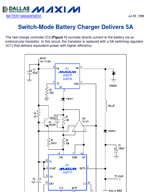
BATTERY MANAGEMENT Jul 09, 1998 Switch-Mode Battery Charger Delivers 5AThe fast-charge controller IC3 (Figure 1) normally directs current to the battery via an external pnp transistor. In this circuit, the transistor is replaced with a 5A switching regulator (IC1) that delivers equivalent power with higher efficiency.Figure 1. By controlling the PWM duty cycle of switching regulator IC1, the fast-charge controller (IC3) makes efficient delivery of the battery's charging current.IC1 is a 5A buck switching regulator whose output is configured as a current source. Its internal power switch (an npn transistor) is relatively efficient because V CE(SAT) is small in comparison with the 15V-to-40V inputs. (For applications that require 2A or less, the low-saturation, non-Darlington power switch of a MAX726 offers better efficiency.)R6 senses the battery-charging current and enables IC3 to generate an analog drive signal at DRV. The signal is first attenuated by the op amp to assure stability by reducing gain in the control loop. It then drives IC1's compensation pin (VC), which gives direct access to the internal PWM comparator. IC3 thus controls the charging current via the PWM duty cycle of IC1. The Q1 buffer provides current to the DRV input.Loop stability is also determined by the feedback loop's dominant pole, set by C4 at the CC terminal of IC3. If you increase the value of the battery filter capacitor (C5), you should make a proportional increase in the value of C4. Lower values, however, assure good transient response. If your application produces load transients during the fast-charge cycle, check the worst-case response to a load step. To assure proper termination of the charge, battery voltage should settle within 2msec to 5mV times N (where N is the number of battery cells). More InformationMAX713:QuickView-- Full (PDF) Data Sheet-- Free Samples。
S7 -1200紧凑型交换机模块CSM1277 操作说明

请注意下列说明:
商标 责任免除
警告 Siemens 产品只允许用于目录和相关技术文件中规定的使用情况。如果要使用其他公司的产品和组件,必须得到 Siemens 推荐和允许。正确的运输、储存、组装、装配、安装、调试、操作和维护是产品安全、正常运行的前 提。必须保证允许的环境条件..................................................................................................................................31
7.1
4.5
双绞线电缆 ......................................................................................................................... 23
4.6
安装IE FC RJ-45 插头 180 ................................................................................................. 24
危险 表示如果不采取相应的小心措施,将会导致死亡或者严重的人身伤害。
警告 表示如果不采取相应的小心措施,可能导致死亡或者严重的人身伤害。
小心 带有警告三角,表示如果不采取相应的小心措施,可能导致轻微的人身伤害。
小心 不带警告三角,表示如果不采取相应的小心措施,可能导致财产损失。
注意 表示如果不注意相应的提示,可能会出现不希望的结果或状态。
4.7
可能产生问题的原因及问题的解决方法 .............................................................................. 26
- 1、下载文档前请自行甄别文档内容的完整性,平台不提供额外的编辑、内容补充、找答案等附加服务。
- 2、"仅部分预览"的文档,不可在线预览部分如存在完整性等问题,可反馈申请退款(可完整预览的文档不适用该条件!)。
- 3、如文档侵犯您的权益,请联系客服反馈,我们会尽快为您处理(人工客服工作时间:9:00-18:30)。
General DescriptionThe MAX1277/MAX1279 are low-power, high-speed, seri-al-output, 12-bit, analog-to-digital converters (ADCs) with an internal reference that operates at up to 1.5Msps.These devices feature true-differential inputs, offering bet-ter noise immunity, distortion improvements, and a wider dynamic range over single-ended inputs. A standard SPI™/QSPI™/MICROWIRE™interface provides the clock necessary for conversion. These devices easily interface with standard digital signal processor (DSP) synchronous serial interfaces.The MAX1277/MAX1279 operate from a single +2.7V to +3.6V supply voltage. The MAX1277/MAX1279 include a 2.048V internal reference. The MAX1277 has a unipolar analog input, while the MAX1279 has a bipolar analog input. These devices feature a partial power-down mode and a full power-down mode for use between conver-sions, which lower the supply current to 2mA (typ) and 1µA (max), respectively. Also featured is a separate power-supply input (V L ), which allows direct interfacing to +1.8V to V DD digital logic. The fast conversion speed,low-power dissipation, excellent AC performance, and DC accuracy (±1 LSB INL) make the MAX1277/MAX1279ideal for industrial process control, motor control, and base-station applications.The MAX1277/MAX1279 come in a 12-pin TQFN pack-age, and are available in the commercial (0°C to +70°C)and extended (-40°C to +85°C) temperature ranges.ApplicationsData Acquisition Communications Bill Validation Portable InstrumentsMotor ControlFeatures♦1.5Msps Sampling Rate♦Only 22mW (typ) Power Dissipation ♦Only 1µA (max) Shutdown Current♦High-Speed, SPI-Compatible, 3-Wire Serial Interface ♦68.5dB S/(N + D) at 525kHz Input Frequency ♦Internal True-Differential Track/Hold (T/H)♦Internal 2.048V Reference ♦No Pipeline Delays♦Small 12-Pin TQFN PackageMAX1277/MAX12791.5Msps, Single-Supply, Low-Power, True-Differential, 12-Bit ADCs with Internal Reference________________________________________________________________Maxim Integrated Products119-3365; Rev 0; 8/04For pricing, delivery, and ordering information,please contact Maxim/Dallas Direct!at 1-888-629-4642, or visit Maxim’s website at .SPI/QSPI are trademarks of Motorola, Inc.MICROWIRE is a trademark of National Semiconductor Corp.M A X 1277/M A X 12791.5Msps, Single-Supply, Low-Power, True-Differential, 12-Bit ADCs with Internal ReferenceABSOLUTE MAXIMUM RATINGSELECTRICAL CHARACTERISTICSStresses beyond those listed under “Absolute Maximum Ratings” may cause permanent damage to the device. These are stress ratings only, and functional operation of the device at these or any other conditions beyond those indicated in the operational sections of the specifications is not implied. Exposure to absolute maximum rating conditions for extended periods may affect device reliability.V DD to GND..............................................................-0.3V to +6V V L to GND................-0.3V to the lower of (V DD + 0.3V) and +6V Digital Inputsto GND.................-0.3V to the lower of (V DD + 0.3V) and +6V Digital Outputto GND....................-0.3V to the lower of (V L + 0.3V) and +6V Analog Inputs andREF to GND..........-0.3V to the lower of (V DD + 0.3V) and +6V RGND to GND.......................................................-0.3V to +0.3VMaximum Current into Any Pin............................................50mA Continuous Power Dissipation (T A = +70°C)12-Pin TQFN (derate 16.9mW/°C above +70°C)......1349mW Operating Temperature RangesMAX127_ _ CTC.................................................0°C to +70°C MAX127_ _ ETC..............................................-40°C to +85°C Junction Temperature......................................................+150°C Storage Temperature Range.............................-60°C to +150°C Lead Temperature (soldering, 10s).................................+300°CMAX1277/MAX12791.5Msps, Single-Supply, Low-Power, True-Differential, 12-Bit ADCs with Internal Reference_______________________________________________________________________________________3ELECTRICAL CHARACTERISTICS (continued)(V DD = +2.7V to +3.6V, V L = V DD , f SCLK = 24MHz, 50% duty cycle, T A = T MIN to T MAX , unless otherwise noted. Typical values are at T A = +25°C.)M A X 1277/M A X 12791.5Msps, Single-Supply, Low-Power, True-Differential, 12-Bit ADCs with Internal Reference 4_______________________________________________________________________________________Note 1:Relative accuracy is the deviation of the analog value at any code from its theoretical value after the gain error and the offseterror have been nulled.Note 2:No missing codes over temperature.Note 3:Conversion time is defined as the number of clock cycles (16) multiplied by the clock period.Note 4:At sample rates below 10ksps, the input full-linear bandwidth is reduced to 5kHz.Note 5:The listed value of three SCLK cycles is given for full-speed continuous conversions. Acquisition time begins on the 14th ris-ing edge of SCLK and terminates on the next falling edge of CNVST. The IC idles in acquisition mode between conversions.Note 6:Undersampling at the maximum signal bandwidth requires the minimum jitter spec for SINAD performance.Note 7:1.5Msps operation guaranteed for V L > 2.7V. See the Typical Operating Characteristics section for recommended samplingspeeds for V L < 2.7V.Note 8:Digital supply current is measured with the V IH level equal to V L , and the V IL level equal to GND.TIMING CHARACTERISTICSFigure 1. Detailed Serial-Interface Timing Figure 2. Load Circuits for Enable/Disable TimesMAX1277/MAX12791.5Msps, Single-Supply, Low-Power, True-Differential, 12-Bit ADCs with Internal Reference_______________________________________________________________________________________5Typical Operating Characteristics(V DD = +3V, V L = V DD , f SCLK = 24MHz, f SAMPLE = 1.5Msps, T A = T MIN to T MAX , unless otherwise noted. Typical values are measured at T A = +25°C.)MAXIMUM RECOMMENDED f SCLK vs. V LM A X 1277/79 t o c 01V L (V)f S C L K (M H z )3.33.02.72.42.119212325171.83.6-1.00-0.75-0.50-0.2500.250.500.751.0001024204830724096INTEGRAL NONLINEARITYvs. DIGITAL OUTPUT CODE (MAX1277)M A X 1277/79 t o c 02DIGITAL OUTPUT CODEI N L (L S B )-1.00-0.75-0.50-0.2500.250.500.751.00-2048-1024010242048INTEGRAL NONLINEARITYvs. DIGITAL OUTPUT CODE (MAX1279)M A X 1277/79 t o c 03DIGITAL OUTPUT CODEI N L (L S B )-1.00-0.75-0.50-0.2500.250.500.751.0001024204830724096DIFFERENTIAL NONLINEARITY vs. DIGITAL OUTPUT CODE (MAX1277)M A X 1277/79 t o c 04DIGITAL OUTPUT CODE D N L (L S B )-1.00-0.75-0.50-0.2500.250.500.751.00-2048-1024010242048DIFFERENTIAL NONLINEARITY vs. DIGITAL OUTPUT CODE (MAX1279)M A X 1277/79 t o c 05DIGITAL OUTPUT CODE D N L (L S B )-6-4-5-2-3-10-4010-15356085OFFSET ERRORvs. TEMPERATURE (MAX1277)M A X 1277/79 t o c 06TEMPERATURE (°C)O F F S E T E R R O R (L S B )-6-4-5-2-3-10-4010-15356085OFFSET ERRORvs. TEMPERATURE (MAX1279)M A X 1277/79 t o c 07TEMPERATURE (°C)O F F S E T E R R O R (L S B )-20-12134-4010-15356085GAIN ERRORvs. TEMPERATURE (MAX1277)M A X 1277/79 t o c 08TEMPERATURE (°C)G A I N E R R O R (L S B )-4-2-30-112-4010-15356085GAIN ERRORvs. TEMPERATURE (MAX1279)M A X 1277/79 t o c 09TEMPERATURE (°C)G A I N E R R O R (L S B )Typical Operating Characteristics (continued)(V DD = +3V, V L = V DD , f SCLK = 24MHz, f SAMPLE = 1.5Msps, T A = T MIN to T MAX , unless otherwise noted. Typical values are measured at T A = +25°C.)M A X 1277/M A X 12791.5Msps, Single-Supply, Low-Power, True-Differential, 12-Bit ADCs with Internal Reference 6_______________________________________________________________________________________70.069.569.068.568.0100300200400500DYNAMIC PERFORMANCE vs. INPUT FREQUENCY (MAX1277)ANALOG INPUT FREQUENCY (kHz)D Y N A M I C PE RF O R M A N C E (d B )70.069.569.068.568.0100300200400500DYNAMIC PERFORMANCEvs. INPUT FREQUENCY (MAX1279)ANALOG INPUT FREQUENCY (kHz)D Y N A M I C PE RF O R M A N C E (d B )-80-84-88-92-96100300200400500THD vs. INPUT FREQUENCYANALOG INPUT FREQUENCY (kHz)T H D (d B )828488869092SFDR vs. INPUT FREQUENCYANALOG INPUT FREQUENCY (kHz)S F D R (d B )100300200400500-140-100-120-60-80-20-4000250375125500625750FFT PLOT (MAX1277)ANALOG INPUT FREQUENCY (kHz)A M P L I T U D E (d B )f IN = 500kHz SINAD = 68.7dB SNR = 68.9dB THD = -83.1dB SFDR = 85.0dB-140-100-120-60-80-20-4000250375125500625750FFT PLOT (MAX1279)ANALOG INPUT FREQUENCY (kHz)A M P L I T U D E (dB )f IN = 500kHz SINAD = 69.0dB SNR = 69.1dB THD = -88.9dB SFDR = 85.9dBMAX1277/MAX12791.5Msps, Single-Supply, Low-Power, True-Differential, 12-Bit ADCs with Internal Reference_______________________________________________________________________________________7TOTAL HARMONIC DISTORTION vs. SOURCE IMPEDANCESOURCE IMPEDANCE (Ω)T H D (d B )100-90-80-70-60-50-100101000TWO-TONE IMD PLOT (MAX1277)ANALOG INPUT FREQUENCY (kHz)A M P L I T U D E (dB )625500375250125-120-100-80-60-40-200-140750TWO-TONE IMD PLOT (MAX1279)ANALOG INPUT FREQUENCY (kHz)A M P L I T U D E (dB )625500375250125-120-100-80-60-40-200-1407500.200.600.400.801.00-4010-15356085V DD /V L FULL POWER-DOWNSUPPLY CURRENT vs. TEMPERATURETEMPERATURE (°C)V D D /V L S U P P L Y C U R R E N T (µA )0502575100-4010-15356085V L PARTIAL/FULL POWER-DOWN SUPPLY CURRENT vs. TEMPERATURETEMPERATURE (°C)V L S U P P L Y C U R R E N T (µA )03.01.56.04.57.59.0-4010-15356085V DD SUPPLY CURRENT vs. TEMPERATURETEMPERATURE (°C)V D D S U P P L Y C U R R E N T (m A )Typical Operating Characteristics (continued)(V DD = +3V, V L = V DD , f SCLK = 24MHz, f SAMPLE = 1.5Msps, T A = T MIN to T MAX , unless otherwise noted. Typical values are measured at T A = +25°C.)M A X 1277/M A X 12791.5Msps, Single-Supply, Low-Power, True-Differential, 12-Bit ADCs with Internal Reference 8_______________________________________________________________________________________Typical Operating Characteristics (continued)(V DD = +3V, V L = V DD , f SCLK = 24MHz, f SAMPLE = 1.5Msps, T A = T MIN to T MAX , unless otherwise noted. Typical values are measured at T A = +25°C.)864200750250500100012501500V DD SUPPLY CURRENT vs. CONVERSION RATEM A X 1277/79 t o c 22f SAMPLE (kHz)V D D S U P P L Y C U R R E N T (m A )00.100.300.200.400.50-4010-15356085V L SUPPLY CURRENT vs. TEMPERATURETEMPERATURE (°C)V L S U P P L Y C U R R E N T (m A )0501501002002500500250750100012501500V L SUPPLY CURRENT vs. CONVERSION RATEf SAMPLE (kHz)V L S U P P L Y C U R R E N T (µA )2.002.022.012.042.032.052.06-4010-15356085REFERENCE VOLTAGE vs. TEMPERATUREM A X 1277/79 t o c 25TEMPERATURE (°C)R E F E R E N C E V O L T A G E (V )2.052.042.032.022.014268REFERENCE VOLTAGE vs. LOAD CURRENT (SOURCE)M A X 1277/79 t o c 26LOAD CURRENT (mA)R E F E R E N C E V O L T A G E (V )2.082.072.062.052.0410050150200REFERENCE VOLTAGE vs. LOAD CURRENT (SINK)M A X 1277/79 t o c 27LOAD CURRENT (µA)R E F E R E N C E V O L T A G E (V )MAX1277/MAX12791.5Msps, Single-Supply, Low-Power, True-Differential, 12-Bit ADCs with Internal ReferencePin DescriptionM A X 1277/M A X 1279True-Differential Analog Input T/HThe equivalent circuit of Figure 4 shows the input archi-tecture of the MAX1277/MAX1279, which is composed of a T/H, a comparator, and a switched-capacitor digi-tal-to-analog converter (DAC). The T/H enters its track-ing mode on the 14th SCLK rising edge of the previous conversion. Upon power-up, the T/H enters its tracking mode immediately. The positive input capacitor is con-nected to AIN+. The negative input capacitor is con-nected to AIN-. The T/H enters its hold mode on the falling edge of CNVST and the difference between the sampled positive and negative input voltages is convert-ed. The time required for the T/H to acquire an input sig-nal is determined by how quickly its input capacitance is charged. If the input signal’s source impedance is high,the acquisition time lengthens. The acquisition time,t ACQ , is the minimum time needed for the signal to be acquired. It is calculated by the following equation:t ACQ ≥9 ×(RS + R IN ) ×16pFwhere R IN = 200Ω, and RS is the source impedance of the input signal.Note:t ACQ is never less than 125ns and any source impedance below 12Ωdoes not significantly affect the ADC’s AC performance.Input BandwidthThe ADC’s input-tracking circuitry has a 15MHz small-signal bandwidth, making it possible to digitize high-speed transient events and measure periodic signals with bandwidths exceeding the ADC’s sampling rate by using undersampling techniques. To avoid high-frequency signals being aliased into the frequency band of interest, anti-alias filtering is recommended.Analog Input ProtectionInternal protection diodes that clamp the analog input to V DD and GND allow the analog input pins to swing from GND - 0.3V to V DD + 0.3V without damage. Both inputs must not exceed V DD or be lower than GND for accurate conversions.Serial InterfaceInitialization After Power-Up and Starting a ConversionUpon initial power-up, the MAX1277/MAX1279 require a complete conversion cycle to initialize the internal cali-bration. Following this initial conversion, the part is ready for normal operation. This initialization is only required after a hardware power-up sequence and is not required after exiting partial or full power-down mode.To start a conversion, pull CNVST low. At CNVST’s falling edge, the T/H enters its hold mode and a conver-sion is initiated. SCLK runs the conversion and the data can then be shifted out serially on DOUT.1.5Msps, Single-Supply, Low-Power, True-Differential, 12-Bit ADCs with Internal Reference10______________________________________________________________________________________Figure 6. SPI Interface—Partial Power-Down ModeFigure 5. Interface-Timing SequenceTiming and ControlConversion-start and data-read operations are con-trolled by the CNVST and SCLK digital inputs. Figures 1and 5 show timing diagrams, which outline the serial-interface operation.A CNVST falling edge initiates a conversion sequence;the T/H stage holds the input voltage, the ADC begins to convert, and DOUT changes from high impedance to logic low. SCLK is used to drive the conversion process, and it shifts data out as each bit of the conver-sion is determined.SCLK begins shifting out the data after the 4th rising edge of SCLK. DOUT transitions t DOUT after each SCLK’s rising edge and remains valid 4ns (t DHOLD )after the next rising edge. The 4th rising clock edge produces the MSB of the conversion at DOUT, and the MSB remains valid 4ns after the 5th rising edge. Since there are 12 data bits and 3 leading zeros, at least 16rising clock edges are needed to shift out these bits.For continuous operation, pull CNVST high between the 14th and the 16th SCLK rising edges. If CNVST stays low after the falling edge of the 16th SCLK cycle, the DOUT line goes to a high-impedance state on either CNVST’s rising edge or the next SCLK’s rising edge.Partial Power-Down and Full Power-Down ModesPower consumption can be reduced significantly by plac-ing the MAX1277/MAX1279 in either partial power-down mode or full power-down mode. Partial power-down mode is ideal for infrequent data sampling and fast wake-up time applications. Pull CNVST high after the 3rd SCLK rising edge and before the 14th SCLK rising edge to enter and stay in partial power-down mode (see Figure 6). This reduces the supply current to 2mA. While in par-tial power-down mode, the reference remains enabled to allow valid conversions once the IC is returned to normal mode. Drive CNVST low and allow at least 14 SCLK cycles to elapse before driving CNVST high to exit partial power-down mode.Full power-down mode is ideal for infrequent data sam-pling and very low supply current applications. The MAX1277/MAX1279 have to be in partial power-down mode to enter full power-down mode. Perform the SCLK/CNVST sequence described above to enter par-tial power-down mode. Then repeat the same sequence to enter full power-down mode (see Figure 7). Drive CNVST low, and allow at least 14 SCLK cycles to elapse before driving CNVST high to exit full power-down mode. While in full power-down mode, the refer-ence is disabled to minimize power consumption. Be sure to allow at least 2ms recovery time after exiting full power-down mode for the reference to settle. In partial/full power-down mode, maintain a logic low or a logic high on SCLK to minimize power consumption.Transfer FunctionFigure 8 shows the unipolar transfer function for the MAX1277. Figure 9 shows the bipolar transfer function for the MAX1279. The MAX1277 output is straight binary,while the MAX1279 output is two’s complement.Applications InformationInternal ReferenceThe MAX1277/MAX1279 have an on-chip voltage refer-ence trimmed to 2.048V. The internal reference output is connected to REF and also drives the internal capac-itive DAC. The output can be used as a reference volt-age source for other components and can source up to 2mA. Bypass REF with a 0.01µF capacitor and a 4.7µF capacitor to RGND.The internal reference is continuously powered up dur-ing both normal and partial power-down modes. In full power-down mode, the internal reference is disabled.Be sure to allow at least 2ms recovery time after hard-ware power-up or exiting full power-down mode for the reference to reach its intended value.MAX1277/MAX1279Differential, 12-Bit ADCs with Internal Reference______________________________________________________________________________________11Figure 7. SPI Interface—Full Power-Down ModeM A X 1277/M A X 1279How to Start a ConversionAn analog-to-digital conversion is initiated by CNVST,clocked by SCLK, and the resulting data is clocked out on DOUT by SCLK. With SCLK idling high or low, a falling edge on CNVST begins a conversion. This causes the analog input stage to transition from track to hold mode,and for DOUT to transition from high impedance to being actively driven low. A total of 16 SCLK cycles are required to complete a normal conversion. If CNVST is low during the 16th falling SCLK edge, DOUT returns to high imped-ance on the next rising edge of CNVST or SCLK, enabling the serial interface to be shared by multiple devices. If CNVST returns high after the 14th, but before the 16th SCLK rising edge, DOUT remains active so continuous conversions can be sustained. The highest throughput is achieved when performing continuous conversions. Figure 10 illustrates a conversion using a typical serial interface.Connection toStandard InterfacesThe MAX1277/MAX1279 serial interface is fully compati-ble with SPI/QSPI and MICROWIRE (see Figure 11). If a serial interface is available, set the CPU’s serial interface in master mode so the CPU generates the serial clock.Choose a clock frequency up to 24MHz.SPI and MICROWIREWhen using SPI or MICROWIRE, the MAX1277/ MAX1279are compatible with all four modes programmed with the CPHA and CPOL bits in the SPI or MICROWIRE control register. Conversion begins with a CNVST falling edge.DOUT goes low, indicating a conversion is in progress.Two consecutive 1-byte reads are required to get the full 12 bits from the ADC. DOUT transitions on SCLK rising edges. DOUT is guaranteed to be valid t DOUT later and remains valid until t DHOLD after the following SCLK rising edge. When using CPOL = 0 and CPHA = 0, or CPOL = 1and CPHA = 1, the data is clocked into the µP on the fol-lowing rising edge. When using CPOL = 0 and CPHA = 1,or CPOL = 1 and CPHA = 0, the data is clocked into the µP on the next falling edge. See Figure 11 for connections and Figures 12 and 13 for timing. See the Timing Characteristics section to determine the best mode to use.QSPIUnlike SPI, which requires two 1-byte reads to acquire the 12 bits of data from the ADC, QSPI allows the mini-mum number of clock cycles necessary to clock in the data. The MAX1277/MAX1279 require 16 clock cycles from the µP to clock out the 12 bits of data. Figure 14shows a transfer using CPOL = 1 and CPHA = 1. The conversion result contains three zeros, followed by the 12 data bits, and a trailing zero with the data in MSB-first format.Differential, 12-Bit ADCs with Internal Reference 12______________________________________________________________________________________Figure 8. Unipolar Transfer Function (MAX1277 Only)Figure 9. Bipolar Transfer Function (MAX1279 Only)MAX1277/MAX1279Differential, 12-Bit ADCs with Internal Reference______________________________________________________________________________________13Figure 11. Common Serial-Interface Connections to the MAX1277/MAX1279Figure 10. Continuous Conversion with Burst/Continuous ClockDSP Interface to the TMS320C54_The MAX1277/MAX1279 can be directly connected to the TMS320C54_ family of DSPs from Texas Instruments, Inc. Set the DSP to generate its own clocks or use external clock signals. Use either the standard or buffered serial port. Figure 15 shows the simplest interface between the MAX1277/MAX1279 and the TMS320C54_, where the transmit serial clock (CLKX) drives the receive serial clock (CLKR) and SCLK, and the transmit frame sync (FSX) drives the receive frame sync (FSR) and CNVST.For continuous conversion, set the serial port to trans-mit a clock, and pulse the frame sync signal for a clock period before data transmission. The serial-port config-uration (SPC) register should be set up with internal frame sync (TXM = 1), CLKX driven by an on-chip clock source (MCM = 1), burst mode (FSM = 1), and 16-bit word length (FO = 0).This setup allows continuous conversions provided that the data transmit register (DXR) and the data-receive register (DRR) are serviced before the next conversion.Alternatively, autobuffering can be enabled when using the buffered serial port to execute conversions and read the data without CPU intervention. Connect the V LM A X 1277/M A X 1279Differential, 12-Bit ADCs with Internal Reference 14______________________________________________________________________________________Figure 13. SPI/MICROWIRE Serial-Interface Timing—Continuous Conversion (CPOL = CPHA = 0), (CPOL = CPHA = 1)000D11D10D9D8D7D6D5D4D3D2D1D00DOUT SCLKCNVST111416Figure 12. SPI/MICROWIRE Serial-Interface Timing—Single Conversion (CPOL = CPHA = 0), (CPOL = CPHA = 1)Figure 14. QSPI Serial-Interface Timing—Single Conversion (CPOL = 1, CPHA = 1)MAX1277/MAX1279Differential, 12-Bit ADCs with Internal Reference______________________________________________________________________________________15pin to the TMS320C54_ supply voltage when the MAX1277/MAX1279 are operating with an analog sup-ply voltage higher than the DSP supply voltage. The word length can be set to 8 bits with FO = 1 to imple-ment the power-down modes. The CNVST pin must idle high to remain in either power-down state.Another method of connecting the MAX1277/MAX1279to the TMS320C54_ is to generate the clock signals external to either device. This connection is shown in Figure 16, where serial clock (CLOCK) drives theCLKR, and SCLK and the convert signal (CONVERT)drive the FSR and CNVST.The serial port must be set up to accept an external receive-clock and external receive-frame sync. The SPC register should be written as follows:TXM = 0, external frame syncMCM = 0, CLKX is taken from the CLKX pin FSM = 1, burst modeFO = 0, data transmitted/received as 16-bit wordsThis setup allows continuous conversion, provided that the DRR is serviced before the next conversion.Alternatively, autobuffering can be enabled when using the buffered serial port to read the data without CPU intervention. Connect the V L pin to the TMS320C54_supply voltage when the MAX1277/MAX1279 are oper-ating with an analog supply voltage higher than the DSP supply voltage.The MAX1277/MAX1279 can also be connected to the TMS320C54_ by using the data transmit (DX) pin to drive CNVST and the CLKX generated internally to drive SCLK. A pullup resistor is required on the CNVST signal to keep it high when DX goes high impedance and 0001hex should be written to the DXR continuously for continuous conversions. The power-down modes may be entered by writing 00FFhex to the DXR (see Figures 17 and 18).DSP Interface to the ADSP21_ _ _The MAX1277/MAX1279 can be directly connected to the ADSP21_ _ _ family of DSPs from Analog Devices,Inc. Figure 19 shows the direct connection of the MAX1277/MAX1279 to the ADSP21_ _ _. There are two modes of operation that can be programmed to interface with the MAX1277/MAX1279. For continuous conver-sions, idle CNVST low and pulse it high for one clock cycle during the LSB of the previous transmitted word.The ADSP21_ _ _ STCTL and SRCTL registers should be configured for early framing (LAFR = 0) and for anFigure 15. Interfacing to the TMS320C54_ Internal ClocksFigure 16. Interfacing to the TMS320C54_ External Clocks000D11D10D9D8D7D6D5D4D3D2D1D00DOUT SCLKCNVST0D011Figure 17. DSP Interface—Continuous ConversionM A X 1277/M A X 1279active-high frame (LTFS = 0, LRFS = 0) signal. In this mode, the data-independent frame-sync bit (DITFS = 1)can be selected to eliminate the need for writing to the transmit-data register more than once. For single conver-sions, idle CNVST high and pulse it low for the entire conversion. The ADSP21_ _ _ STCTL and SRCTL regis-ters should be configured for late framing (LAFR = 1)and for an active-low frame (LTFS = 1, LRFS = 1) signal.This is also the best way to enter the power-down modes by setting the word length to 8 bits (SLEN = 1001).Connect the V L pin to the ADSP21_ _ _ supply voltage when the MAX1277/MAX1279 are operating with a sup-ply voltage higher than the DSP supply voltage (see Figures 17 and 18).Layout, Grounding, and BypassingFor best performance, use PC boards. Wire-wrap boards are not recommended. Board layout should ensure that digital and analog signal lines are separat-ed from each other. Do not run analog and digital (especially clock) lines parallel to one another, or digital lines underneath the ADC package.Figure 20 shows the recommended system ground connections. Establish a single-point analog ground (star ground point) at GND, separate from the logic ground. Connect all other analog grounds and DGND to this star ground point for further noise reduction. The ground return to the power supply for this ground should be low impedance and as short as possible for noise-free operation.High-frequency noise in the V DD power supply can affect the ADC’s high-speed comparator. Bypass this supply to the single-point analog ground with 0.01µF and 10µF bypass capacitors. Minimize capacitor lead lengths for best supply-noise rejection.DefinitionsIntegral NonlinearityIntegral nonlinearity (INL) is the deviation of the values on an actual transfer function from a straight line. This straight line can be either a best-straight-line fit or a line drawn between the end points of the transfer function,once offset and gain errors have been nullified. The static linearity parameters for the MAX1277/MAX1279 are mea-sured using the end-points method.Differential, 12-Bit ADCs with Internal Reference 16______________________________________________________________________________________Figure 20. Power-Supply Grounding ConditionFigure 18. DSP Interface—Single-Conversion, Continuous/Burst Clock。