MAX5426BEUD中文资料
MAX541中文资料

19-1082; Rev 2; 12/99
+5V, Serial-Input, Voltage-Output, 16-Bit DACs
General Description
The MAX541/MAX542 are serial-input, voltage-output, 16-bit digital-to-analog converters (DACs) that operate from a single +5V supply. They provide 16-bit performance (±1LSB INL and DNL) over temperature without any adjustments. The DAC output is unbuffered, resulting in a low supply current of 0.3mA and a low offset error of 1LSB. The DAC output range is 0V to VREF. For bipolar operation, matched scaling resistors are provided in the MAX542 for use with an external precision op amp (such as the MAX400), generating a ±V REF output swing. The MAX542 also includes Kelvin-sense connections for the reference and analog ground pins to reduce layout sensitivity. A 16-bit serial word is used to load data into the DAC latch. The 10MHz, 3-wire serial interface is compatible with SPI™/QSPI™/MICROWIRE™, and it also interfaces directly with optocouplers for applications requiring isolation. A power-on reset circuit clears the DAC output to 0V (unipolar mode) when power is initially applied. The MAX541 is available in 8-pin plastic DIP and SO packages. The MAX542 is available in 14-pin plastic DIP and SO packages. o +5V Single-Supply Operation o Low Power: 1.5mW o 1µs Settling Time o Unbuffered Voltage Output Directly Drives 60kΩ Loads o SPI/QSPI/MICROWIRE-Compatible Serial Interface o Power-On Reset Circuit Clears DAC Output to 0V (unipolar mode) o Schmitt Trigger Inputs for Direct Optocoupler Interface
工业电流电压输出驱动器,输出范围可编程

AD5748Rev. AInformation furnished by Analog Devices is believed to be accurate and reliable. However, noresponsibility is assumed by Analog Devices for its use, nor for any infringements of patents or other rights of third parties that may result from its use. Speci cations subject to change without notice. No license is granted by implication or otherwise under any patent or patent rights of Analog Devices. T rademarks and registered trademarks are the property of their respective owners.One Technology Way, P.O. Box 9106, Norwood, MA 02062-9106, U.S.A.Tel: 781.329.4700 Fax: 781.461.3113 ©2010 Analog Devices, Inc. All rights reserved.表1. 相关器件产品型号描述AD5422工业电流/电压输出驱动器, 输出范围可编程主要特性电流输出范围:4 mA至21 mA、0mA至21 mA总不可调整误差(TUE):±0.15% FSR输出温漂:±5 ppm/°C FSR(典型值)电压输出范围:0 V至5 V、0 V至10.5 V、±10.5 V 总不可调整误差(TUE):±0.05% FSR输出温漂:±3 ppm/°C FSR(典型值)灵活的串行数字接口片内输出故障检测PEC差错校验异步CLEAR(清零)功能灵活的上电状态(0 V或三态)电源电压范围AVDD :+12 V (± 10%)至+24 V (± 10%)AVSS:-12 V (± 10%)至-24 V (± 10%)输出环路顺从电压:AVDD – 2.75 V温度范围:-40℃至+105℃32引脚5 mm × 5 mm LFCSP封装应用过程控制执行器控制PLC(可编程控制器)概述AD5748是一款单通道、低成本、高精度、电压/电流输出驱动器,输出范围可通过硬件或软件编程。
MAX144AEUA中文资料
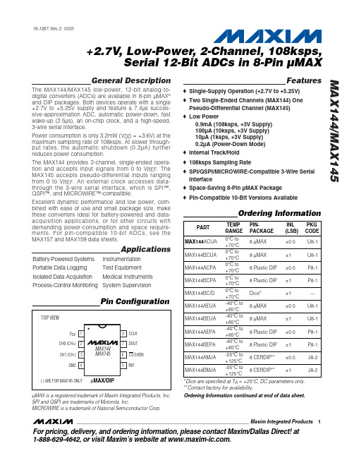
6 5
GND 4
( ) ARE FOR MAX145 ONLY
µMAX/DIP
*Dice are specified at TA = +25°C, DC parameters only. **Contact factory for availability. Ordering Information continued at end of data sheet.
ELECTRICAL CHARACTERISTICS
(V DD = +2.7V to +5.25V, V REF = 2.5V, 0.1µF capacitor at REF, f SCLK = 2.17MHz, 16 clocks/conversion cycle (108ksps), CH- = GND for MAX145, TA = TMIN to TMAX, unless otherwise noted. Typical values are at TA = +25°C.) PARAMETER DC ACCURACY (Note 1) Resolution Relative Accuracy (Note 2) Differential Nonlinearity Offset Error Gain Error Gain Temperature Coefficient Channel-to-Channel Offset Matching Channel-to-Channel Gain Matching (Note 3) ±0.8 ±0.05 ±0.05 RES INL DNL MAX14_A MAX14_B No missing codes over temperature 12 ±0.5 ±1 ±0.75 ±3 ±3 Bits LSB LSB LSB LSB ppm/°C LSB LSB SYMBOL CONDITIONS MIN TYP MAX UNITS
MAX4466EXK中文资料

5-Pin SC70 (derate 2.5mW/°C above +70°C) .............200mW 5-Pin SOT23 (derate 7.1mW/°C above +70°C) ...........571mW
ELECTRICAL CHARACTERISTICS
(VCC = +5V, VCM = 0, VOUT = VCC/2, RL = ∞ to VCC/2, SHDN = GND (MAX4467/MAX4468 only). TA = TMIN to TMAX, unless otherwise noted. Typical values specified at TA = +25°C.) (Note 1)
TOP VIEW
IN+ 1
5 VCC
MAX4465 GND 2 MAX4466
IN- 3
4 OUT
SC70/SOT23 Pin Configurations continued at end of data sheet.
Rail-to-Rail is a registered trademark of Nippon Motorola, Ltd.
Features
o +2.4V to +5.5V Supply Voltage Operation
o Versions with 5nA Complete Shutdown Available (MAX4467/MAX4468)
MAX232中文资料,MAX232CPE,MAX232EPE,MAX232ECPE,规格书,MAXIM代理商,datasheet,PDF
19-4323; Rev 15; 13;5V ޥ٫Ăۂ لRS-232 ഝڑಹ/ेฏಹ
________________________________ ݣะ
MAX220–MAX249࿅઼ഝڑಹ /ेฏಹLjከཛྷEIA/TIA232EჾࣆV.28/V.24ဳेਊහࣜLjᅐದกྐۨ໗ ޥ±12V ٫ᆚوᄮᅋă
ሦဗಹऔ໎Ӽคࠩ٫֠ޥ٫࿅༇Ljሦกᅑᅢದّڱߔࠞޢ ன৹ჾटࠞޢऋဏ ف5μW ჾăMAX225ĂMAX233Ă MAX235 ჾࣆ MAX245/MAX246/MAX247 ԥၖე༶ԩᆐ औLj༚ऌᅋᅢᄩฺ٫ଁғஎࢵᅘوᄮᅋă
1.0 (0.1) 0.1 — — 1.0 (0.1) — 1.0 (0.1) 1.0 (0.1) 1.0 (0.1) 1.0 (0.1)
1.0 1.0 (0.1) 0.1 0.1 1.0 — — — 1.0 1.0
SHDN & ThreeState No Yes Yes Yes Yes No
No No No No No Yes Yes No No No
_____________________________________________________________________ ၭျӹ
Part Number MAX220 MAX222 MAX223 (MAX213) MAX225 MAX230 (MAX200) MAX231 (MAX201)
MAX232 (MAX202) MAX232A MAX233 (MAX203) MAX233A MAX234 (MAX204) MAX235 (MAX205) MAX236 (MAX206) MAX237 (MAX207) MAX238 (MAX208) MAX239 (MAX209)
AD5422中文资料
Single Channel, 16-Bit, Serial Input,Current Source & Voltage Output DAC Preliminary Technical Data AD5422Rev. PrEInformation furnished by Analog Devices is believed to be accurate and reliable. However, noresponsibility is assumed by Analog Devices for its use, nor for any infringements of patents or other rights of third parties that may result from its use. Specifications subject to change without notice. No license is granted by implication or otherwise under any patent or patent rights of Analog Devices. T rademarks and registered trademarks are the property of their respective owners. One Technology Way, P.O. Box 9106, Norwood, M A 02062-9106, U.S.A. Tel: 781.329.4700 Fax: 781.461.3113 ©2007 Analog Devices, Inc. All rights reserved.FEATURES16-Bit Resolution and MonotonicityCurrent Output Ranges: 4–20mA, 0–20mA or 0–24mA 0.1% typ Total Unadjusted Error (TUE)5ppm/°C Output DriftVoltage Output Ranges: 0-5V, 0-10V, ±5V, ±10V,10% over-range0.05% Total Unadjusted Error (TUE)3ppm/°C Output DriftFlexible Serial Digital InterfaceOn-Chip Output Fault DetectionOn-Chip Reference (10 ppm/°C Max)Asynchronous CLEAR FunctionPower Supply RangeAV DD : 10.8V to 40 VAV SS : -26.4V to -3V/0VOutput Loop Compliance to AV DD – 2.5 V Temperature Range: -40°C to +85°CTSSOP and LFCSP PackagesAPPLICATIONSProcess ControlActuator ControlPLC GENERAL DESCRIPTIONThe AD5422 is a low-cost, precision, fully integrated 16-bit converter offering a programmable current source and programmable voltage output designed to meet the requirements of industrial process control applications.The output current range is programmable to 4mA to 20 mA,0mA to 20mA or an overrange function of 0mA to 24mA. Voltage output is provided from a separate pin that can be configured to provide 0V to 5V, 0V to 10V, ±5V or ±10V output ranges, an over-range of 10% is available on all ranges. Analog outputs are short and open circuit protected and can drive capacitive loads of 1uF and inductive loads of 1H.The device is specified to operate with a power supply range from 10.8 V to 40 V. Output loop compliance is 0 V to AV DD – 2.5 V.The flexible serial interface is SPI and MICROWIRE compatible and can be operated in 3-wire mode to minimize the digital isolation required in isolated applications.The device also includes a power-on-reset function ensuring that the device powers up in a known state and an asynchronous CLEAR pin which sets the outputs to zero-scale / mid-scale voltage output or the low end of the selected current range.The total output error is typically ±0.1% in current mode and ±0.05% in voltage mode.Table 1. Related DevicesPart Number DescriptionAD5412 Single Channel, 12-Bit, SerialInput Current Source andVoltage Output DACAD5420 Single Channel, 16-Bit, SerialInput Current Source DACAD5410 Single Channel, 12-Bit, SerialInput Current Source DACAD5422Preliminary Technical DataRev. PrE | Page 2 of 37TABLE OF CONTENTSFeatures..............................................................................................1 Applications.......................................................................................1 General Description.........................................................................1 Revision History...............................................................................2 Functional Block Diagram..............................................................3 Specifications.....................................................................................4 AC Performance Characteristics................................................7 Timing Characteristics................................................................8 Absolute Maximum Ratings..........................................................10 ESD Caution................................................................................10 Pin Configuration and Function Descriptions...........................11 Typical Performance Characteristics Voltage output ...............13 Typical Performance Characteristics current output ...............17 Typical Performance Characteristics general ............................20 Terminology....................................................................................22 Theory of Operation......................................................................24 Architecture.................................................................................24 Serial Interface............................................................................24 Default configuration.................................................................28 Transfer Function.......................................................................28 Data Register...............................................................................29 Control Register..........................................................................29 RESET register............................................................................29 Status register..............................................................................30 Features............................................................................................31 fault alert......................................................................................31 voltage output short circuit protection....................................31 Asynchronous Clear (CLEAR).................................................31 Internal Reference......................................................................31 External current setting resistor...............................................31 Voltage ouTput over-range........................................................31 Digital Power Supply..................................................................31 External boost function.............................................................31 digital Slew rate control.............................................................32 I OUT Filtering Capacitors............................................................32 Applications Information..............................................................33 driving inductive loads..............................................................33 Transient voltage protection.....................................................33 Layout Guidelines.......................................................................33 Galvanically Isolated Interface.................................................33 Microprocessor Interfacing.......................................................33 Thermal and supply considerations.........................................34 Outline Dimensions.......................................................................35 Ordering Guide.. (35)REVISION HISTORYPrE – Preliminary Version, November 22, 2007Preliminary Technical DataAD5422Rev. PrE | Page 3 of 37FUNCTIONAL BLOCK DIAGRAMV OUT I OUT LATCH SCLK SDIN SDOCCAGND CLEAR FAULT BOOSTREFOUT REFIN SENSESENSECLEAR SELECT R SET DV CC C COMP2C COMP1DGND**LFCSP PackageFigure 1.AD5422Preliminary Technical DataRev. PrE | Page 4 of 37SPECIFICATIONSAV DD = 10.8V to 40V , AV SS = -26.4V to -3V/0V , AV DD + |AV SS | < 52.8V , AGND = DGND = 0 V , REFIN= +5 V external; DV CC = 2.7 V to 5.5 V , V OUT : R L = 2 kΩ, C L = 200 pF, I OUT : R L = 300Ω, H L = 50mH; all specifications T MIN to T MAX , ±10 V / 0 to 24 mA range unless otherwise noted. Table 2.Parameter Value 1 Unit Test Conditions/CommentsVOLTAGE OUTPUTOutput Voltage Ranges 0 to 5 V 0 to 10 V -5 to +5 V -10 to +10 V ACCURACY Output unloaded Bipolar Output Resolution 16 Bits Total Unadjusted Error (TUE) 0.1 % FSR max Over temperature, supplies, and time, typically 0.05%FSRTUE TC 2 ±3 ppm typ Relative Accuracy (INL) ±0.012 % FSR max Differential Nonlinearity (DNL) ±1 LSB max Guaranteed monotonic Bipolar Zero Error ±5 mV max @ 25°C, error at other temperatures obtained usingbipolar zero TCBipolar Zero TC 2±3 ppm FSR/°C max Zero-Scale Error ±1 mV max @ 25°C, error at other temperatures obtained using zeroscale TCZero-Scale TC 2±3 ppm FSR/°C max Gain Error ±0.05 % FSR max @ 25°C, error at other temperatures obtained using gainTCGain TC 2 ±8 ppm FSR/°C max Full-Scale Error 0.05 % FSR max @ 25°C, error at other temperatures obtained using gainTCFull-Scale TC 2 ±3 ppm FSR/°C max Unipolar Output AV SS = 0 V Resolution 16 Bits Total Unadjusted Error (TUE) 0.1 % FSR max Over temperature, supplies, and time, typically 0.05%FSRRelative Accuracy (INL) ±0.012 % FSR max Differential Nonlinearity (DNL) ±1 LSB max Guaranteed monotonic (at 16 bit-resolution) Zero Scale Error +10 mV max @ 25°C, error at other temperatures obtained using gainTCZero Scale TC 2±3 ppm FSR/°C max Offset Error ±10 mV max Gain Error ±0.05 % FSR max @ 25°C, error at other temperatures obtained using gainTCGain TC 2±3 ppm FSR/°C max Full-Scale Error 0.05 % FSR max @ 25°C, error at other temperatures obtained using gainTCFull-Scale TC 2±3 ppm FSR/°C maxOUTPUT CHARACTERISTICS 2eadroom 0.8 V max 0.5 V typ Output Voltage TC ±3 ppm FSR/°C max Output Voltage Drift vs. Time ±12 ppm FSR/500 hr typ Vout = ¾ of Full-Scale ±15 ppm FSR/1000 hr typ Short-Circuit Current 12 mA typPreliminary Technical DataAD5422Rev. PrE | Page 5 of 37Parameter Value 1 Unit Test Conditions/Comments Load 2 kΩ min For specified performance Capacitive Load Stability R L = ∞ 20 nF max R L = 2 kΩ TBD nF max R L = ∞ 1 µF max External compensation capacitor of 4nF connected. DC Output Impedance 0.3 Ω typ Power-On Time 10 µs typ DC PSRR TBD µV/VCURRENT OUTPUTOutput Current Ranges 0 to 24 mA 0 to 20 mA 4 to 20 mA ACCURACY Resolution 16 Bits Total Unadjusted Error (TUE) ±0.3 % FSR max Over temperature, supplies, and time, typically 0.1% FSR TUE TC 2 ±5 ppm/°C typ Relative Accuracy (INL) ±0.012 % FSR max Differential Nonlinearity (DNL) ±1 LSB max Guaranteed monotonic Offset Error ±0.05 % FSR max Offset Error Drift ±5 µv/°C typ Gain Error ±0.02 % FSR max @ 25°C, error at other temperatures obtained using gainTCGain TC 2 ±8 ppm FSR/°C max Full-Scale Error 0.05 % FSR max @ 25°C, error at other temperatures obtained using gainTCFull-Scale TC 2 ±8 ppm FSR/°COUTPUT CHARACTERISTICS 2Current Loop Compliance Voltage AVDD - 2.5 V max Output Current Drift vs. Time TBD ppm FSR/500 hr typ TBD ppm FSR/1000 hr typ Resistive Load TBD Ω max Inductive Load 1 H max DC PSRR 10 µA/V max Output Impedance 50 MΩ typREFERENCE INPUT/OUTPUTReference Input 2 Reference Input Voltage 5 V nom ±1% for specified performance DC Input Impedance 30 kΩ min Typically 40 kΩ Reference Range 4 to 5 V min to V max Reference Output Output Voltage 4.998 to 5.002 V min to V max @ 25°C Reference TC ±10 ppm/°C max Output Noise (0.1 Hz to 10 Hz)2 18 µV p-p typNoise Spectral Density 2120 nV/√Hz typ @ 10 kHz Output Voltage Drift vs. Time 2 ±40 ppm/500 hr typ ±50 ppm/1000 hr typ Capacitive Load TBD nF max Load Current 5 mA typ Short Circuit Current 7 mA typ Line Regulation 2 10 ppm/V typLoad Regulation 2TBD ppm/mA Thermal Hysteresis 2 TBD ppmAD5422 Preliminary Technical Data1 Temperature range: -40°C to +85°C; typical at +25°C.2 Guaranteed by characterization. Not production tested.Rev. PrE | Page 6 of 37Preliminary Technical DataAD5422Rev. PrE | Page 7 of 37AC PERFORMANCE CHARACTERISTICSAV DD = 10.8V to 40V , AV SS = -26.4V to -3V/0V , AV DD + |AV SS | < 52.8V , AGND = DGND = 0 V , REFIN= +5 V external; DV CC = 2.7 V to 5.5 V , V OUT : R L = 2 kΩ, C L = 200 pF, I OUT : R L = 300Ω, H L = 50mH; all specifications T MIN to T MAX , ±10 V / 0 to 24 mA range unless otherwise noted. Table 3.Parameter 1 Unit Test Conditions/Comments DYNAMIC PERFORMANCEVOLTAGE OUTPUTOutput Voltage Settling Time 8 µs typ Full-scale step (10 V) to ±0.03% FSR 10 µs max 5 µs max 512 LSB step settlingOutput Current Settling Time 10 µs max To 0.1% FSR Slew Rate 1 V/µs typ Power-On Glitch Energy 10 nV-sec typ Digital-to-Analog Glitch Energy 10 nV-sec typ Glitch Impulse Peak Amplitude 20 mV typ Digital Feedthrough 1 nV-sec typ Output Noise (0.1 Hz to 10 Hz Bandwidth) 0.1 LSB p-p typ Output Noise (100 kHz Bandwidth) 80 µV rms max 1/f Corner Frequency 1 kHz typ Output Noise Spectral Density 100 nV/√Hz typ Measured at 10 kHz AC PSRR TBD dB 200mV 50/60Hz Sinewavesuperimposed on power supply voltage.CURRENT OUTPUTOutput Current Settling Time TBD µs typ To 0.1% FSR , L = 1H TBD µs typ To 0.1% FSR , L < 1mH1Guaranteed by characterization, not production tested.AD5422Preliminary Technical DataRev. PrE | Page 8 of 37TIMING CHARACTERISTICSAV DD = 10.8V to 40V , AV SS = -26.4V to -3V/0V , AV DD + |AV SS | < 52.8V , AGND = DGND = 0 V , REFIN= +5 V external; DV CC = 2.7 V to 5.5 V , V OUT : R L = 2 kΩ, C L = 200 pF, I OUT : R L = 300Ω, H L = 50mH; all specifications T MIN to T MAX , ±10 V / 0 to 24 mA range unless otherwise noted. Table 4.Parameter 1, 2, 3 Limit at T MIN , T MAX Unit DescriptionWrite Modet 1 33 ns min SCLK cycle time t 2 13 ns min SCLK low time t 3 13 ns min SCLK high time t 4 13 ns min LATCH delay time t 5 40 ns min LATCH high time t 5 5 µs min LATCH high time (After a write to the CONTROL register) t 6 5 ns min Data setup time t 7 5 ns min Data hold time t 8 40 ns min LATCH low time t 9 20 ns min CLEAR pulsewidth t 10 5 µs max CLEAR activation timeReadback Modet 11 82 ns min SCLK cycle time t 12 33 ns min SCLK low time t 13 33 ns min SCLK high time t 14 13 ns min LATCH delay time t 15 40 ns min LATCH high time t 16 5 ns min Data setup time t 17 5 ns min Data hold time t 18 40 ns min LATCH low time t 19 40 ns max Serial output delay time (C L SDO 4 = 15pF) t 20 33 ns max LATCH rising edge to SDO tri-stateDaisychain Modet 21 82 ns min SCLK cycle time t 22 33 ns min SCLK low time t 23 33 ns min SCLK high time t 24 13 ns min LATCH delay time t 25 40 ns min LATCH high time t 26 5 ns min Data setup time t 27 5 ns min Data hold time t 28 40 ns min LATCH low time t 29 40 ns max Serial output delay time (C L SDO 4 = 15pF)1 Guaranteed by characterization. Not production tested.2All input signals are specified with t R = t F = 5 ns (10% to 90% of DV CC ) and timed from a voltage level of 1.2 V. 3See Figure 2, Figure 3, and Figure 4. 4C L SDO = Capacitive load on SDO output.Preliminary Technical DataAD5422Rev. PrE | Page 9 of 37SCLK LATCHSDINCLEAROUTPUTFigure 2. Write Mode Timing DiagramSCLKLATCHSDINSDOSELECTED REGISTER DATA CLOCKED OUTFIRST 8 BITS ARE DON’T CARE BITSFigure 3. Readback Mode Timing DiagramSCLKSDINSDOLATCHFigure 4. Daisychain Mode Timing DiagramAD5422Preliminary Technical DataRev. PrE | Page 10 of 37ABSOLUTE MAXIMUM RATINGST A = 25°C unless otherwise noted.Transient currents of up to 100 mA do not cause SCR latch-up. Table 5.Parameter Rating AV DD to AGND, DGND −0.3V to 48V AV SS to AGND, DGND +0.3 V to −48 V AV DD to AV SS -0.3V to 60V DV CC to AGND, DGND −0.3 V to +7 V Digital Inputs to AGND, DGND −0.3 V to DV CC + 0.3 V or 7 V(whichever is less)Digital Outputs to AGND, DGND −0.3 V to DV CC + 0.3 V or 7V(whichever is less)REFIN/REFOUT to AGND, DGND −0.3 V to +7 V V OUT to AGND, DGND AV SS to AV DD I OUT to AGND, DGND −0.3V to AV DD AGND to DGND -0.3V to +0.3V Operating Temperature Range Industrial −40°C to +851°C Storage Temperature Range −65°C to +150°C Junction Temperature (T J max) 125°C 24-Lead TSSOP Package θJA Thermal Impedance 42°C/W 40-Lead LFCSP Package θJA Thermal Impedance 28°C/W Power Dissipation (T J max – T A )/ θJA Lead Temperature JEDEC Industry StandardSoldering J-STD-020Stresses above those listed under Absolute Maximum Ratings may cause permanent damage to the device. This is a stress rating only; functional operation of the device at these or any other conditions above those indicated in the operationalsection of this specification is not implied. Exposure to absolute maximum rating conditions for extended periods may affect device reliability.ESD CAUTION1Power dissipated on chip must be de-rated to keep junction temperature below 125°C. Assumption is max power dissipation condition is sourcing 24mA into Ground from AV DD with a 3mA on-chip current.PIN CONFIGURATION AND FUNCTION DESCRIPTIONSAGND SDOAV SSSENSE GNDLATCH CLEAR CLEAR SELECT REFIN SELECT SCLK SDIN GND R SETOUTBOOST C COMP1REFOUT DV CC C COMP2I OUTSENSEAV DDDV CCD G N G N A V S CA V S SA V D D N CN CV S E N S EV C CNCNC DV CC SELECT V S E N S EO U TBOOST C COMP1C COMP2I OUT N R S E NC A G N CN N R E F I R E F O U CAP2CAP1Figure 5. TSSOP Pin ConfigurationFigure 6. LFCSP Pin ConfigurationTSSOP Pin No. LFCSP Pin No. Mnemonic Descriptionoutputpin.19 26 I OUT Current20 27 BOOSTOptional external transistor connection. Connecting an external transistor will reducethe power dissipated in the AD5422. Refer to the features section.N/A 28 CAP1 Connection for optional output filtering capacitor. Refer to Features section.N/A 29 CAP2 Connection for optional output filtering capacitor. Refer to Features section.21 32 V OUT Buffered Analog Output Voltage. The output amplifier is capable of directly driving a 2kΩ, 2000 pF load.22 33 +V SENSE Sense connection for the positive voltage output load connection.23 34 -V SENSE Sense connection for the negative voltage output load connection.24 36 AV DD Positive Analog Supply Pin. Voltage ranges from 10.8V to 60V.Paddle Paddle AV SS Negative Analog Supply Pin. Voltage ranges from –3 V to –24 V. This pin can beconnected to 0V if output voltage range is unipolar.TYPICAL PERFORMANCE CHARACTERISTICSVOLTAGE OUTPUTFigure 7. Integral Non Linearity Error vs DAC Code (Four Traces)Figure 8. Differential Non Linearity Error vs. DAC Code (Four Traces)Figure 9. Total Unadjusted Error vs. DAC Code (Four Traces)Figure 10. Integral Non Linearity vs. Temperature (Four Traces)Figure 11. Differential Non Linearity vs. Temperature (Four Traces)Figure 12. Integral Non Linearity vs. Supply Voltage (Four Traces)Figure 13.Differential Non Linearity Error vs. Supply Voltage (Four Traces)Figure 14. Integral Non Linearity Error vs. Reference Voltage (Four traces)Figure 15. Differential Non Linearity Error vs. Reference Voltage (Four Traces)Figure 16. Total Unadjusted Error vs.Reference Voltage (Four Traces)Figure 17. Total Unadjusted Error vs. Supply Voltage (Four Traces)Figure 18. Offset Error vs.TemperatureFigure 19. Bipolar Zero Error vs. TemperatureFigure 20. Gain Error vs. TemperatureFigure 21. Source and Sink Capability of Output AmplifierFull-Scale Code LoadedFigure 22. Source and Sink Capability of Output AmplifierZero-Scale LoadedFigure 23.Full-Scale Positive StepFigure 24. Full-Scale Negative StepFigure 25. Digital-to-Analog Glitch EnergyFigure 26. Peak-to-Peak Noise (0.1Hz to 10Hz Bandwidth)Figure 27. Peak-to-Peak Noise (100kHz Bandwidth)Figure 28. V OUT vs. Time on Power-upFigure 29. V OUT vs, Time on Output EnabledTYPICAL PERFORMANCE CHARACTERISTICS CURRENT OUTPUTFigure 30. Integral Non Linearity vs. CodeFigure 31.Differential Non Linearity vs. CodeFigure 32. Total Unadjusted Error vs. CodeFigure 33. Integral Non Linearity vs. TemperatureFigure 34. Differential Non Linearity vs. TemperatureFigure 35. Integral Non Linearity vs. SupplyFigure 36. Differential Non Linearity vs. Supply VoltageFigure 37. Integral Non Linearity vs. Reference VoltageFigure 38. Differential Non Linearity vs. Reference VoltageFigure 39. Total Unadjusted Error vs. Reference VoltageFigure 40. Total Unadjusted Error vs. Supply VoltageFigure 41. Offset Error vs. TemperatureFigure 42. Gain Error vs. TemperatureFigure 43. Voltage Compliance vs. TemperatureFigure 44. I OUT vs. Time on Power-upFigure 45. I OUT vs. Time on Output EnabledTYPICAL PERFORMANCE CHARACTERISTICS GENERALFigure 46. DI CC vs.Logic Input VoltageFigure 47. AI DD /AI SS vs AV DD /AV SSFigure 48. AI DD vs AV DDFigure 49. DVCC Output Voltage vs. DI CC Load CurrentFigure 50. Refout Turn-on TransientFigure 51. Refout Output Noise (0.1Hz to 10Hz Bandwidth)Figure 52. Refout Output Noise (100kHz Bandwidth)Figure 53. Refout Line TransientFigure 54. Refout Load TransientFigure 55. Refout Histogram of Thermal HysteresisFigure 56. Refout Voltage vs. Load CurrentTERMINOLOGYRelative Accuracy or Integral Nonlinearity (INL)For the DAC, relative accuracy, or integral nonlinearity (INL), is a measure of the maximum deviation, in LSBs, from a straight line passing through the endpoints of the DAC transfer function. A typical INL vs. code plot can be seen in Figure 7. Differential Nonlinearity (DNL)Differential nonlinearity (DNL) is the difference between the measured change and the ideal 1 LSB change between any two adjacent codes. A specified differential nonlinearity of ±1 LSB maximum ensures monotonicity. This DAC is guaranteed monotonic by design. A typical DNL vs. code plot can be seen in Figure 10.MonotonicityA DAC is monotonic if the output either increases or remains constant for increasing digital input code. The AD5724R/AD5734R/AD5754R are monotonic over their full operating temperature range.Bipolar Zero ErrorBipolar zero error is the deviation of the analog output from the ideal half-scale output of 0 V when the DAC register is loaded with 0x8000 (straight binary coding) or 0x0000 (twos complement coding). A plot of bipolar zero error vs. temperature can be seen in Table TBD.Bipolar Zero TCBipolar zero TC is a measure of the change in the bipolar zero error with a change in temperature. It is expressed in ppm FSR/°C.Full-Scale ErrorFull-Scale error is a measure of the output error when full-scale code is loaded to the DAC register. Ideally, the output should be full-scale − 1 LSB. Full-scale error is expressed in percent offull-scale range (% FSR).Negative Full-Scale Error/Zero-Scale ErrorNegative full-scale error is the error in the DAC output voltage when 0x0000 (straight binary coding) or 0x8000 (twos complement coding) is loaded to the DAC register. Ideally, the output voltage should be negative full-scale− 1 LSB. A plot of zero-scale error vs. temperature can be seen in Table TBD Zero-Scale TCThis is a measure of the change in zero-scale error with a change in temperature. Zero-scale error TC is expressed in ppm FSR/°C. Output Voltage Settling TimeOutput voltage settling time is the amount of time it takes for the output to settle to a specified level for a full-scale input change. A plot of settling time can be seen in Table TBD Slew RateThe slew rate of a device is a limitation in the rate of change of the output voltage. The output slewing speed of a voltage-output D/A converter is usually limited by the slew rate of the amplifier used at its output. Slew rate is measured from 10% to 90% of the output signal and is given in V/µs.Gain ErrorThis is a measure of the span error of the DAC. It is the deviation in slope of the DAC transfer characteristic from ideal expressed in % FSR. A plot of gain error vs. temperature can be seen in Table TBDGain TCThis is a measure of the change in gain error with changes in temperature. Gain Error TC is expressed in ppm FSR/°C. Total Unadjusted ErrorTotal unadjusted error (TUE) is a measure of the output error taking all the various errors into account, namely INL error, offset error, gain error, and output drift over supplies, temperature, and time. TUE is expressed in % FSR.Current Loop Voltage ComplianceThe maximum voltage at the I OUT pin for which the output currnet will be equal to the programmed value.Power-On Glitch EnergyPower-on glitch energy is the impulse injected into the analog output when the AD5422 is powered-on. It is specified as the area of the glitch in nV-sec. See Table TBDDigital-to-Analog Glitch ImpulseDigital-to-analog glitch impulse is the impulse injected into the analog output when the input code in the DAC register changes state, but the output voltage remains constant. It is normally specified as the area of the glitch in nV-sec and is measured when the digital input code is changed by 1 LSB at the major carry transition (0x7FFF to 0x8000). See Table TBDGlitch Impulse Peak AmplitudeGlitch impulse peak amplitude is the peak amplitude of the impulse injected into the analog output when the input code in the DAC register changes state. It is specified as the amplitude of the glitch in mV and is measured when the digital input code is changed by 1 LSB at the major carry transition (0x7FFF to0x8000). See Table TBD.Digital FeedthroughDigital feedthrough is a measure of the impulse injected into the analog output of the DAC from the digital inputs of the DAC, but is measured when the DAC output is not updated. It is specified in nV-sec and measured with a full-scale code change on the data bus.Power Supply Rejection Ratio (PSRR)PSRR indicates how the output of the DAC is affected by changes in the power supply voltage.Reference TCReference TC is a measure of the change in the reference output voltage with a change in temperature. It is expressed in ppm/°C. Line RegulationLine regulation is the change in reference output voltage due to a specified change in supply voltage. It is expressed in ppm/V. Load RegulationLoad regulation is the change in reference output voltage due to a specified change in load current. It is expressed in ppm/mA. Thermal HysteresisThermal hysteresis is the change of reference output voltage after the device is cycled through temperatures from +25°C to −40°C to +85°C and back to +25°C. This is a typical value from a sample of parts put through such a cycle. See Table TBDfor a histogram of thermal hysteresis.TCOOHYSOVVV__C)25(−°=6__10C)25(C)25()(×°−°=OTCOOHYSO VVVppmVwhere:V O(25°C) = V O at 25°CV O_TC = V O at 25°C after temperature cycleTHEORY OF OPERATIONThe AD5422 is a precision digital to current loop and voltage output converter designed to meet the requirements of industrial process control applications. It provides a high precision, fully integrated, low cost single-chip solution for generating current loop and unipolar/bipolar voltage outputs. The current ranges available are; 0 to 20mA, 0 to 24mA and 4 to 20mA, the voltage ranges available are; 0 to 5V , ±5V , 0 to 10V and ±10V , the current and voltage outputs are available onseparate pins and only one is active at any one time. The desired output configuration is user selectable via the CONTROL register.ARCHITECTUREThe DAC core architecture of the AD5422 consists of two matched DAC sections. A simplified circuit diagram is shown in Figure 57. The 4 MSBs of the 16-bit data word are decoded to drive 15 switches, E1 to E15. Each of these switches connects 1 of 15 matched resistors to either ground or the reference buffer output. The remaining 12 bits of the data-word drive switches S0 to S11 of a 12-bit voltage mode R-2R ladder network.V REFV OUT12-BIT R-2R LADDE RFOUR MSBs DECODED INTO 15 EQUAL SEGMENTSFigure 57. DAC Ladder StructureThe voltage output from the DAC core is either converted to a current (see diagram, Figure 58) which is then mirrored to the supply rail so that the application simply sees a current source output with respect to ground or it is buffered and scaled to output a software selectable unipolar or bipolar voltage range (See diagram, Figure 59). The current and voltage are output onseparate pins and cannot be output simultaneously.I OUTFigure 58. Voltage to Current conversion circuitryREFINL1Figure 59. Voltage OutputVoltage Output AmplifierThe voltage output amplifier is capable of generating both unipolar and bipolar output voltages. It is capable of driving a load of 2 kΩ in parallel with 1 µF to AGND. The source and sink capabilities of the output amplifier can be seen in Figure TBD. The slew rate is 1 V/µs with a full-scale settling time of 10 µs, (10V step). Figure 59 shows the voltage output drving a load, R L on top of a common mode voltage of up to ±3V .In output module applications where a cable could possibly become disconnected from +V SENSE resulting in the amplifier loop being broken and most probably resulting in largedestructive voltages on V OUT , a resistor, R 1, of value 2k Ω to 5k Ω should be included as shown to ensure the amplifier loop is kept closed.Driving Large Capacitive LoadsThe voltage output amplifier is capable of driving capacitive loads of up to 1uF with the addition of a non-polarised 4nF compensation capacitor between the C COMP1 and C COMP2 pins. Without the compensation capacitor, up to 20nF capacitive loads can be driven.Reference BuffersThe AD5422 can operate with either an external or internal reference. The reference input has an input range of 4 V to 5 V , 5 V for specified performance. This input voltage is then buffered before it is applied to the DAC.SERIAL INTERFACEThe AD5422 is controlled over a versatile 3-wire serial interface that operates at clock rates up to 30 MHz. It is compatible with SPI®, QSPI™, MICROWIRE™, and DSP standards.Input Shift RegisterThe input shift register is 24 bits wide. Data is loaded into the device MSB first as a 24-bit word under the control of a serial clock input, SCLK. Data is clocked in on the rising edge of SCLK. The input register consists of 8 control bits and 16 data bits as shown in Table 7. The 24 bit word is unconditionally latched on the rising edge of LATCH. Data will continue to be clocked in irrespective of the state of LATCH, on the rising edge of LATCH the data that is present in the input register will be latched, in other words the last 24 bits to be clocked in before。
MAX262中文资料
M A X262中文资料(总5页) -CAL-FENGHAI.-(YICAI)-Company One1-CAL-本页仅作为文档封面,使用请直接删除在电子电路中,滤波器是不可或缺的部分,其中有源滤波器更为常用。
一般有源滤波器由运算放大器和RC元件组成,对元器件的参数精度要求比较高,设计和调试也比较麻烦。
美国Maxim公司生产的可编程滤波器芯片MAX262可以通过编程对各种低频信号实现低通、高通、带通、带阻以及全通滤波处理,且滤波的特性参数如中心频率、品质因数等,可通过编程进行设置,电路的外围器件也少。
本文介绍MAX262的情况以及由它构成的程控滤波器电路。
1 MAX262芯片介绍MAX262芯片是Maxim公司推出的双二阶通用开关电容有源滤波器,可通过微处理器精确控制滤波器的传递函数(包括设置中心频率、品质因数和工作方式)。
它采用CMOS工艺制造,在不需外部元件的情况下就可以构成各种带通、低通、高通、陷波和全通滤波器。
图1是它的引脚排列情况。
图1 MAX262引脚V+ ——正电源输入端。
V- ——负电源输入端。
GND ——模拟地。
CLKA ——外接晶体振荡器和滤波器A 部分的时钟输入端,在滤波器内部,时钟频率被2分频。
CLKB ——滤波器B 部分的时钟输入端,同样在滤波器内部,时钟频率被2分频。
CLKOUT ——晶体振荡器和R-C振荡的时钟输出端。
OSCOUT ——与晶体振荡器或R-C振荡器相连,用于自同步。
INA、INB ——滤波器的信号输入端。
BPA、BPB——带通滤波器输出端。
LPA、LPB——低通滤波器输出端。
HPA、HPB——高通、带阻、全通滤波器输出端。
WR ——写入有效输入端。
接V+时,输人数据不起作用;接V-时,数据可通过逻辑接口进入一个可编程的内存之中,以完成滤波器的工作模式、f0及Q的设置。
此外,还可以接收TTL电平信号,并上升沿锁存输人数据。
A0、A1、A2、A3 ——地址输人端,可用来完成对滤波器工作模式、f0和Q的相应设置。
max485esa中文资料
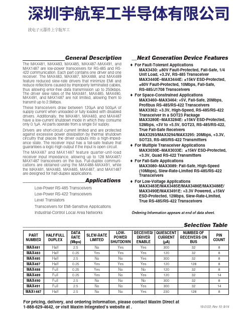
General DescriptionThe MAX481, MAX483, MAX485, MAX487–MAX491, andMAX1487 are low-power transceivers for RS-485 and RS-422 communication. Each part contains one driver and onereceiver. The MAX483, MAX487, MAX488, and MAX489feature reduced slew-rate drivers that minimize E MI andreduce reflections caused by improperly terminated cables,thus allowing error-free data transmission up to 250kbps.The driver slew rates of the MAX481, MAX485, MAX490,MAX491, and MAX1487 are not limited, allowing them totransmit up to 2.5Mbps.These transceivers draw between 120µA and 500µA ofsupply current when unloaded or fully loaded with disableddrivers. Additionally, the MAX481, MAX483, and MAX487have a low-current shutdown mode in which they consumeonly 0.1µA. All parts operate from a single 5V supply.Drivers are short-circuit current limited and are protectedagainst excessive power dissipation by thermal shutdowncircuitry that places the driver outputs into a high-imped-ance state. The receiver input has a fail-safe feature thatguarantees a logic-high output if the input is open circuit.The MAX487 and MAX1487 feature quarter-unit-loadreceiver input impedance, allowing up to 128 MAX487/MAX1487 transceivers on the bus. Full-duplex communi-cations are obtained using the MAX488–MAX491, whilethe MAX481, MAX483, MAX485, MAX487, and MAX1487are designed for half-duplex applications.________________________Applications Low-Power RS-485 Transceivers Low-Power RS-422 Transceivers Level Translators Transceivers for EMI-Sensitive Applications Industrial-Control Local Area Networks__Next Generation Device Features o For Fault-Tolerant Applications MAX3430: ±80V Fault-Protected, Fail-Safe, 1/4Unit Load, +3.3V, RS-485 Transceiver MAX3440E–MAX3444E: ±15kV ESD-Protected,±60V Fault-Protected, 10Mbps, Fail-Safe, RS-485/J1708 Transceivers o For Space-Constrained Applications MAX3460–MAX3464: +5V, Fail-Safe, 20Mbps,Profibus RS-485/RS-422 Transceivers MAX3362: +3.3V, High-Speed, RS-485/RS-422Transceiver in a SOT23 Package MAX3280E–MAX3284E: ±15kV ESD-Protected,52Mbps, +3V to +5.5V, SOT23, RS-485/RS-422,True Fail-Safe Receivers MAX3293/MAX3294/MAX3295: 20Mbps, +3.3V,SOT23, RS-485/RS-422 Transmitters o For Multiple Transceiver Applications MAX3030E–MAX3033E: ±15kV ESD-Protected,+3.3V, Quad RS-422 Transmitters o For Fail-Safe Applications MAX3080–MAX3089: Fail-Safe, High-Speed (10Mbps), Slew-Rate-Limited RS-485/RS-422Transceiverso For Low-Voltage ApplicationsMAX3483E/MAX3485E/MAX3486E/MAX3488E/MAX3490E/MAX3491E: +3.3V Powered, ±15kVESD-Protected, 12Mbps, Slew-Rate-Limited,True RS-485/RS-422 Transceivers For pricing, delivery, and ordering information, please contact Maxim Direct at1-888-629-4642, or visit Maxim Integrated’s website at .______________________________________________________________Selection Table19-0122; Rev 10; 9/14PARTNUMBERHALF/FULL DUPLEX DATA RATE (Mbps) SLEW-RATE LIMITED LOW-POWER SHUTDOWN RECEIVER/DRIVER ENABLE QUIESCENT CURRENT (μA) NUMBER OF RECEIVERS ON BUS PIN COUNT MAX481Half 2.5No Yes Yes 300328MAX483Half 0.25Yes Yes Yes 120328MAX485Half 2.5No No Yes 300328MAX487Half 0.25Yes Yes Yes 1201288MAX488Full 0.25Yes No No 120328MAX489Full 0.25Yes No Yes 1203214MAX490Full 2.5No No No 300328MAX491Full 2.5No No Yes 3003214MAX1487 Half 2.5No No Yes 2301288Ordering Information appears at end of data sheet.找电子元器件上宇航军工MAX481/MAX483/MAX485/MAX487–MAX491/MAX1487Low-Power, Slew-Rate-LimitedRS-485/RS-422 TransceiversPackage Information For the latest package outline information and land patterns, go to . Note that a “+”, “#”, or “-”in the package code indicates RoHS status only. Package drawings may show a different suffix character, but the drawing pertains to the package regardless of RoHS status.16Low-Power, Slew-Rate-Limited RS-485/RS-422 TransceiversMAX481/MAX483/MAX485/MAX487–MAX491/MAX1487Maxim Integrated cannot assume responsibility for use of any circuitry other than circuitry entirely embodied in a Maxim Integrated product. No circuit patent licenses are implied. Maxim Integrated reserves the right to change the circuitry and specifications without notice at any time. The parametric values (min and max limits) shown in the Electrical Characteristics table are guaranteed. Other parametric values quoted in this data sheet are provided for guidance.Maxim Integrated 160 Rio Robles, San Jose, CA 95134 USA 1-408-601-100017©2014 Maxim Integrated Products, Inc.Maxim Integrated and the Maxim Integrated logo are trademarks of Maxim Integrated Products, Inc.。
- 1、下载文档前请自行甄别文档内容的完整性,平台不提供额外的编辑、内容补充、找答案等附加服务。
- 2、"仅部分预览"的文档,不可在线预览部分如存在完整性等问题,可反馈申请退款(可完整预览的文档不适用该条件!)。
- 3、如文档侵犯您的权益,请联系客服反馈,我们会尽快为您处理(人工客服工作时间:9:00-18:30)。
General DescriptionThe MAX5426 is a precision resistor network optimized for use with programmable instrumentation amplifiers.The MAX5426 operates from dual ±5V to ±15V supplies and consumes less than 40µA of supply current.Designed to be used in the traditional three op amp instrumentation amplifier topology, this device provides noninverting gains of 1, 2, 4, and 8 that are accurate to 0.025% (A-grade), 0.09% (B-grade), or 0.5% (C-grade) over the extended temperature range (-40°C to +85°C). The MAX5426 is available in the 6.4mm ✕5mm 14-pin TSSOP package.ApplicationsGeneral-Purpose Programmable Instrumentation AmplifiersGain Control in RF Power Amplifiers Precision Dual AttenuatorFeatureso Differential Gains: A V = 1, 2, 4, 8o Gain Accurate to 0.025%, 0.09%, or 0.5% o Dual Supply ±5V to ±15V Operation o Low 36µA Supply Currento Simple CMOS/TTL Logic Compatible 2-Wire Parallel Interface o Space-Saving 14-Pin TSSOP Package (6.4mm ✕5mm)o OFFSET Pin Available to Offset the Output of the Differential AmplifierMAX5426Precision Resistor Network forProgrammable Instrumentation Amplifiers________________________________________________________________Maxim Integrated Products 1Ordering Information19-2318; Rev 0; 1/02For pricing, delivery, and ordering information,please contact Maxim/Dallas Direct!at 1-888-629-4642, or visit Maxim’s website at .Typical Operating CircuitPin Configuration and Functional Diagram appear at end of data sheet.M A X 5426Precision Resistor Network forProgrammable Instrumentation Amplifiers 2_______________________________________________________________________________________ABSOLUTE MAXIMUM RATINGSELECTRICAL CHARACTERISTICSStresses beyond those listed under “Absolute Maximum Ratings” may cause permanent damage to the device. These are stress ratings only, and functional operation of the device at these or any other conditions beyond those indicated in the operational sections of the specifications is not implied. Exposure to absolute maximum rating conditions for extended periods may affect device reliability.V DD to GND............................................................-0.3V to +17V V SS to GND.............................................................-17V to +0.3V D0, D1 to GND...........................................-0.3V to (V DD + 0.2V)D0, D1 to GND (V DD > +6V).................................-0.3V to +6.0V All Other Pins to GND......................(V SS - 0.3V) to (V DD + 0.2V)Maximum Current Into V DD , V SS , D1, D0.........................±50mA Maximum Current from OUT1 to CM or OUT2..............±0.72mAMaximum Current from OUT1 to INDIF- or OUT............±0.72mA Maximum Current from OUT2 to INDIF+ or OFFSET.....±0.72mA Continuous Power Dissipation (T A = +70°C)14-Pin TSSOP (derate 9.1mW/°C above +70°C)..........727mW Operating Temperature Range ...........................-40°C to +85°C Junction Temperature......................................................+150°C Storage Temperature Range.............................-60°C to +150°CMAX5426Precision Resistor Network forProgrammable Instrumentation Amplifiers_______________________________________________________________________________________3Note 2:Each stage (input stage and output stage) is tested for accuracy separately and combined to give the total gain accuracy.The input stage is tested as follows: OUT1 = 10V, OUT2 = 0. Output stage is tested as follows OUT1 = 10V, OUT2 = 0 and OUT2 = 10V, OFFSET = 0.Note 3:Gain of 1 configuration is open circuit (infinite impedance).Note 4:Equivalent load at each pin is calculated according to instrumentation amplifier configuration and assumes ideal op amps.Note 5:See Timing Diagram.ELECTRICAL CHARACTERISTICS (continued)M A X 5426Precision Resistor Network forProgrammable Instrumentation Amplifiers 4_______________________________________________________________________________________Typical Operating Characteristics(V DD = +15V, V SS = -15V, T A = +25°C, unless otherwise noted.)MAX5426A GAIN ACCURACYvs. TEMPERATURETEMPERATURE (°C)G A I N A C C U R A C Y (%)8065-25-105352050-0.015-0.010-0.00500.0050.0100.0150.020-0.020-40MAX5426A GAIN ACCURACY vs. POSITIVE SUPPLY VOLTAGEPOSITIVE SUPPLY VOLTAGE (V)G A I N A C C U R A C Y (%)14.7512.7510.758.756.75-0.012-0.010-0.008-0.006-0.004-0.00200.0020.0040.006-0.0144.75MAX5426A GAIN ACCURACY vs. NEGATIVE SUPPLY VOLTAGENEGATIVE SUPPLY VOLTAGE (V)G A I N A C C U R A C Y (%)-5-7-13-11-9-0.015-0.010-0.00500.0050.0100.0150.020-0.020-15MAX5426B GAIN ACCURACYvs. TEMPERATURETEMPERATURE (°C)G A I N A C C U R A C Y (%)80604020-20-0.025-0.020-0.015-0.010-0.00500.005-0.030-40MAX5426B GAIN ACCURACY vs. POSITIVE SUPPLY VOLTAGEPOSITIVE SUPPLY VOLTAGE (V)G A I N A C C U R A C Y (%)14.7512.7510.758.756.75-0.025-0.020-0.015-0.010-0.00500.005-0.0304.7503961215-40-2020406080POSITIVE SUPPLY CURRENTvs. TEMPERATURETEMPERATURE (°C)P O S I TI V E S U P P L Y C U R R E N T (µA )-10-8-6-4-20-40-10-2552035506580NEGATIVE SUPPLY CURRENTvs. TEMPERATURETEMPERATURE (°C)N E G A T I V E S U P P LY C U R R E N T (µA )5151025203035515POSITIVE SUPPLY CURRENT vs. POSITIVE SUPPLY VOLTAGEPOSITIVE SUPPLY VOLTAGE (V)P O S I T I V E S U P P L Y C U R R E N T (µA)971113-1.2-0.8-1.0-0.4-0.6-0.20-15-5NEGATIVE SUPPLY CURRENT vs. NEGATIVE SUPPLY VOLTAGENEGATIVE SUPPLY VOLTAGE (V)N E G A T I V E S U P P L Y C U R R E N T (µA )-11-13-9-7MAX5426Precision Resistor Network forProgrammable Instrumentation Amplifiers_______________________________________________________________________________________5Detailed DescriptionThe MAX5426 is a precision resistor network with low temperature drift and high accuracy that performs the same function as a precision resistor array and CMOS switches. Operationally, this device consists of fixed resistors and digitally controlled variable resistors that provide differential gains of 1, 2, 4, and 8 (see Functional Diagram ). The MAX5426 provides gains accurate to 0.025% (MAX5426A), 0.09% (MAX5426B)or 0.5% (MAX5426C).The MAX5426 is ideal for programmable instrumenta-tion amplifiers. An offset pin is available to apply a DC offset voltage to the output of the differential amplifier.Pin CM is the common-mode input voltage and can be buffered and connected to the common-mode input of the instrumentation amplifier (usually the shield of the input cable to reduce the effects of cable capacitance and leakage).Digital Interface OperationThe MAX5426 features a simple two-bit parallel pro-gramming interface. D1 and D0 program the gain set-ting according to the Logic-Control Truth Tab le (see Table 1). The digital interface is CMOS/TTL logic com-patible.Timing DiagramFigure 3 shows the timing diagram of MAX5426 for two cases. In case 1, the differential input changes are at OUT1 and OUT2, while the voltage settling is observed at FB1 and FB2. The settling time (t SETTLE ) is defined as the time for the output voltage (from the change in the input) to reach (and stay) within 0.02% of its final value.In case 2, the differential inputs (OUT1 and OUT2) are at constant voltages, while D1 and D0 are varied (for example from 01 to 10) to make a change in the gain.No op amps are used in these cases.Pin DescriptionM A X 5426Precision Resistor Network forProgrammable Instrumentation Amplifiers 6_______________________________________________________________________________________Applications InformationThe MAX5426 is ideal for programmable instrumentation amplifier applications. The typical application circuit of Figure 1 uses the MAX5426 in classical instrumentation amplifier configurations. Two digital inputs set the gain to 1, 2, 4, or 8.Op Amp Selection GuidelinesSelection of an op amp for instrumentation amplifier cir-cuits depends on the accuracy requirements of the specific application. General guidelines are to choose an op amp with sufficient open-loop gain, low input-off-set voltage, and a high common-mode rejection ratio.High open-loop gain is needed to increase the gain accuracy, while low input-offset voltage and low input-offset current help meet gain and offset requirements.Other parameters such as low input capacitance, low input bias current, high input common-mode range,and low noise often need to be considered for a wide input voltage range stability and AC considerations.The MAX427 is an excellent choice to use with the MAX5426.Stereo Audio-Taper AttenuatorFigure 2 shows the application of the MAX5426 as a dual attenuator that can be used in stereo audio systems.Power Supplies and BypassingThe MAX5426 operates from dual ±5V to ±15V sup-plies. In many applications the MAX5426 does not require bypassing. If power-supply noise is excessive,bypass V DD and V SS with 0.1µF ceramic capacitors to GND.Layout ConcernsFor best performance, reduce parasitic board capaci-tance by minimizing the circuit board trace from ampli-fier outputs to inverting inputs. Also choose op amps with low input capacitance.Figure 1. Programmable Instrumentation Amplifier Using MAX5426MAX5426Precision Resistor Network forProgrammable Instrumentation Amplifiers_______________________________________________________________________________________7Figure 2. Stereo Audio-Taper AttenuatorFigure 3. Timing DiagramM A X 5426Precision Resistor Network forProgrammable Instrumentation Amplifiers 8_______________________________________________________________________________________Chip InformationTRANSISTOR COUNT: 126PROCESS TECHNOLOGY: BICMOSPin ConfigurationFunctional DiagramMAX5426Precision Resistor Network forProgrammable Instrumentation AmplifiersMaxim cannot assume responsib ility for use of any circuitry other than circuitry entirely emb odied in a Maxim product. No circuit patent licenses are implied. Maxim reserves the right to change the circuitry and specifications without notice at any time.Maxim Integrated Products, 120 San Gabriel Drive, Sunnyvale, CA 94086 408-737-7600 _____________________9©2002 Maxim Integrated ProductsPrinted USAis a registered trademark of Maxim Integrated Products.Package Information。