CD74HCT241M96中文资料
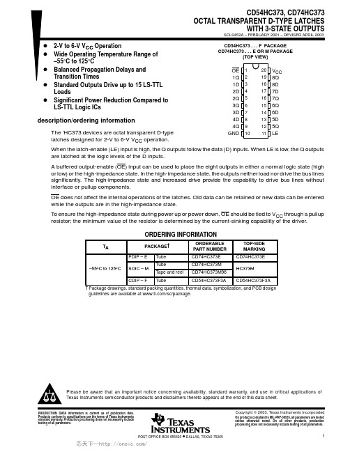
CD74HC373M96,CD74HC373M96,CD74HC373M96,CD74HC373E,CD74HC373M,CD74HC373M96E4,, 规格书,Datasheet 资料
Addendum-Page 1PACKAGING INFORMATIONOrderable Device Status(1)Package Type PackageDrawingPins Package QtyEco Plan(2)Lead/Ball FinishMSL Peak Temp (3)Samples (Requires Login)CD54HC373F ACTIVE CDIP J 201TBD A42N / A for Pkg Type CD54HC373F3A ACTIVE CDIP J 201TBDA42N / A for Pkg TypeCD74HC373E ACTIVE PDIP N 2020Pb-Free (RoHS)CU NIPDAU N / A for Pkg Type CD74HC373EE4ACTIVE PDIP N 2020Pb-Free (RoHS)CU NIPDAU N / A for Pkg Type CD74HC373M ACTIVE SOIC DW 2025Green (RoHS & no Sb/Br)CU NIPDAU Level-1-260C-UNLIM CD74HC373M96ACTIVE SOIC DW 202000Green (RoHS & no Sb/Br)CU NIPDAU Level-1-260C-UNLIM CD74HC373M96E4ACTIVE SOIC DW 202000Green (RoHS & no Sb/Br)CU NIPDAU Level-1-260C-UNLIM CD74HC373M96G4ACTIVE SOIC DW 202000Green (RoHS & no Sb/Br)CU NIPDAU Level-1-260C-UNLIM CD74HC373ME4ACTIVE SOIC DW 2025Green (RoHS & no Sb/Br)CU NIPDAU Level-1-260C-UNLIM CD74HC373MG4ACTIVESOICDW2025Green (RoHS & no Sb/Br)CU NIPDAU Level-1-260C-UNLIM(1)The marketing status values are defined as follows:ACTIVE: Product device recommended for new designs.LIFEBUY: TI has announced that the device will be discontinued, and a lifetime-buy period is in effect.NRND: Not recommended for new designs. Device is in production to support existing customers, but TI does not recommend using this part in a new design.PREVIEW: Device has been announced but is not in production. Samples may or may not be available.OBSOLETE: TI has discontinued the production of the device.(2)Eco Plan - The planned eco-friendly classification: Pb-Free (RoHS), Pb-Free (RoHS Exempt), or Green (RoHS & no Sb/Br) - please check /productcontent for the latest availability information and additional product content details.TBD: The Pb-Free/Green conversion plan has not been defined.Pb-Free (RoHS): TI's terms "Lead-Free" or "Pb-Free" mean semiconductor products that are compatible with the current RoHS requirements for all 6 substances, including the requirement that lead not exceed 0.1% by weight in homogeneous materials. Where designed to be soldered at high temperatures, TI Pb-Free products are suitable for use in specified lead-free processes.Pb-Free (RoHS Exempt): This component has a RoHS exemption for either 1) lead-based flip-chip solder bumps used between the die and package, or 2) lead-based die adhesive used between the die and leadframe. The component is otherwise considered Pb-Free (RoHS compatible) as defined above.Green (RoHS & no Sb/Br): TI defines "Green" to mean Pb-Free (RoHS compatible), and free of Bromine (Br) and Antimony (Sb) based flame retardants (Br or Sb do not exceed 0.1% by weight in homogeneous material)(3)MSL, Peak Temp. -- The Moisture Sensitivity Level rating according to the JEDEC industry standard classifications, and peak solder temperature.芯天下--/Important Information and Disclaimer:The information provided on this page represents TI's knowledge and belief as of the date that it is provided. TI bases its knowledge and belief on information provided by third parties, and makes no representation or warranty as to the accuracy of such information. Efforts are underway to better integrate information from third parties. TI has taken and continues to take reasonable steps to provide representative and accurate information but may not have conducted destructive testing or chemical analysis on incoming materials and chemicals. TI and TI suppliers consider certain information to be proprietary, and thus CAS numbers and other limited information may not be available for release.In no event shall TI's liability arising out of such information exceed the total purchase price of the TI part(s) at issue in this document sold by TI to Customer on an annual basis.OTHER QUALIFIED VERSIONS OF CD54HC373, CD74HC373 :•Catalog: CD74HC373•Military: CD54HC373NOTE: Qualified Version Definitions:•Catalog - TI's standard catalog product•Military - QML certified for Military and Defense ApplicationsAddendum-Page 2芯天下--/TAPE AND REEL INFORMATION*All dimensions are nominalDevicePackage Type Package Drawing Pins SPQReel Diameter (mm)Reel Width W1(mm)A0(mm)B0(mm)K0(mm)P1(mm)W (mm)Pin1Quadrant CD74HC373M96SOICDW202000330.024.410.813.02.712.024.0Q1*All dimensions are nominalDevice Package Type Package Drawing Pins SPQ Length(mm)Width(mm)Height(mm)CD74HC373M96SOIC DW202000367.0367.045.0IMPORTANT NOTICETexas Instruments Incorporated and its subsidiaries(TI)reserve the right to make corrections,enhancements,improvements and other changes to its semiconductor products and services per JESD46C and to discontinue any product or service per JESD48B.Buyers should obtain the latest relevant information before placing orders and should verify that such information is current and complete.All semiconductor products(also referred to herein as“components”)are sold subject to TI’s terms and conditions of sale supplied at the time of order acknowledgment.TI warrants performance of its components to the specifications applicable at the time of sale,in accordance with the warranty in TI’s terms and conditions of sale of semiconductor products.Testing and other quality control techniques are used to the extent TI deems necessary to support this warranty.Except where mandated by applicable law,testing of all parameters of each component is not necessarily performed.TI assumes no liability for applications assistance or the design of Buyers’products.Buyers are responsible for their products and applications using TI components.To minimize the risks associated with Buyers’products and applications,Buyers should provide adequate design and operating safeguards.TI does not warrant or represent that any license,either express or implied,is granted under any patent right,copyright,mask work right,or other intellectual property right relating to any combination,machine,or process in which TI components or services are rmation published by TI regarding third-party products or services does not constitute a license to use such products or services or a warranty or endorsement e of such information may require a license from a third party under the patents or other intellectual property of the third party,or a license from TI under the patents or other intellectual property of TI.Reproduction of significant portions of TI information in TI data books or data sheets is permissible only if reproduction is without alteration and is accompanied by all associated warranties,conditions,limitations,and notices.TI is not responsible or liable for such altered rmation of third parties may be subject to additional restrictions.Resale of TI components or services with statements different from or beyond the parameters stated by TI for that component or service voids all express and any implied warranties for the associated TI component or service and is an unfair and deceptive business practice. TI is not responsible or liable for any such statements.Buyer acknowledges and agrees that it is solely responsible for compliance with all legal,regulatory and safety-related requirements concerning its products,and any use of TI components in its applications,notwithstanding any applications-related information or support that may be provided by TI.Buyer represents and agrees that it has all the necessary expertise to create and implement safeguards which anticipate dangerous consequences of failures,monitor failures and their consequences,lessen the likelihood of failures that might cause harm and take appropriate remedial actions.Buyer will fully indemnify TI and its representatives against any damages arising out of the use of any TI components in safety-critical applications.In some cases,TI components may be promoted specifically to facilitate safety-related applications.With such components,TI’s goal is to help enable customers to design and create their own end-product solutions that meet applicable functional safety standards and requirements.Nonetheless,such components are subject to these terms.No TI components are authorized for use in FDA Class III(or similar life-critical medical equipment)unless authorized officers of the parties have executed a special agreement specifically governing such use.Only those TI components which TI has specifically designated as military grade or“enhanced plastic”are designed and intended for use in military/aerospace applications or environments.Buyer acknowledges and agrees that any military or aerospace use of TI components which have not been so designated is solely at the Buyer's risk,and that Buyer is solely responsible for compliance with all legal and regulatory requirements in connection with such use.TI has specifically designated certain components which meet ISO/TS16949requirements,mainly for automotive ponents which have not been so designated are neither designed nor intended for automotive use;and TI will not be responsible for any failure of such components to meet such requirements.Products ApplicationsAudio /audio Automotive and Transportation /automotiveAmplifiers Communications and Telecom /communicationsData Converters Computers and Peripherals /computersDLP®Products Consumer Electronics /consumer-appsDSP Energy and Lighting /energyClocks and Timers /clocks Industrial /industrialInterface Medical /medicalLogic Security /securityPower Mgmt Space,Avionics and Defense /space-avionics-defense Microcontrollers Video and Imaging /videoRFID OMAP Mobile Processors /omap TI E2E Community Wireless Connectivity /wirelessconnectivityMailing Address:Texas Instruments,Post Office Box655303,Dallas,Texas75265Copyright©2012,Texas Instruments Incorporated。
M74HCT241资料

M54HCT240/241/244M74HCT240/241/244Septembe r 1993HCT240:INVERTED -HCT241/244NON INVERTEDOCTAL BUS BUFFER WITH 3STATE OUTPUTS B1R(Plastic Package)ORDER CODES :M54HCTXXXF1R M74HCTXXXM1R M74HCTXXXB1R M74HCTXXXC1RF1R(Ceramic Package)M1R(Micro Package)C1R (Chip Carrier)PIN CONNECTION (top view).HIGH SPEEDt PD =13ns (TYP.)at V CC =5V .LOW POWER DISSIPATIONI CC =4µA (MAX.)at T A =25oC.COMPATIBLE WITH TTL OUTPUTS V IH =2V (MIN.)V IL =0.8V (MAX).OUTPUT DRIVE CAPABILITY 15LSTTL LOADS.SYMMETRICAL OUTPUT IMPEDANCE |I OH |=I OL =6mA (MIN).BALANCED PROPAGATION DELAYS t PLH =t PHL.PIN AND FUNCTION COMPATIBLE WITH 54/74LS240/241/244DESCRIPTIONThe M54/74HCT240,HCT241and HCT244are high speed CMOS OCTAL BUS BUFFERs fabricated in silicon gate C 2MOS technology.They have the same high speed performance of LSTTL combined with true CMOS low power consumption.The designer has a choise of select combination of inverting and non-inverting outputs,symmetrical G (active low output control)input,and complementary G and G inputs.Each control input governs four BUS BUFFERs.This integrated circuit has input and output characteristics that are fully compatible with 54/74LSTTL logic families.M54/74HCT devices are designed to directly interface HSC 2MOS systems with TTL and NMOS components.They are also plug in replacements for LSTTL devices giving a reduction of power consumption.These devices are designed to be used with 3state memory address drivers,etc.All inputs are equipp ed with protection circuits against static discharge and transient excess voltage.HCT244HCT241HCT2401/12CHIP CARRIERINPUT AND OUTPUT EQUIVALENT CIRCUIT PIN DESCRIPTION (HCT240)PIN No SYMBOL NAME AND FUNCTION 11G Output Enable Input 2,4,6,81A1to 1A4Data Inputs 9,7,5,32Y1to 2Y4Data Outputs 11,13,15,172A1to 2A4Data Inputs 18,16,14,121Y1to 1Y4Data Outputs 192G Output Enabel Input 10GND Ground (0V)20V CCPositive Supply VoltagePIN DESCRIPTION (HCT244)PIN No SYMBOL NAME AND FUNCTION 11G Output Enable Input 2,4,6,81A1to 1A4Data Inputs 9,7,5,32Y1to 2Y4Data Outputs 11,13,15,172A1to 2A4Data Inputs 18,16,14,121Y1to 1Y4Data Outputs 192G Output Enabel Input 10GND Ground (0V)20V CCPositive Supply VoltagePIN DESCRIPTION (HCT241)PIN No SYMBOL NAME AND FUNCTION 11G Output Enable Input 2,4,6,81A1to 1A4Data Inputs 9,7,5,32Y1to 2Y4Data Outputs 11,13,15,172A1to 2A4Data Inputs 18,16,14,121Y1to 1Y4Data Outputs 192G Output Enabel Input 10GND Ground (0V)20V CCPositive Supply VoltageHCT244HCT241HCT240M54/M74HCT240/241/2442/12IEC LOGIC SYMBOLSTRUTH TABLEINPUTOUTPUTG G (HCT241)An Yn (HCT240)Yn (HCT241)Yn (HCT244)L H L H L L L HH LHHHLXZZZX:”H”or ”L”Z:High impeda nceCIRCUIT SCHEMATIC (1/8PACKAGE)HCT244HCT241HCT240HCT240HCT241/244M54/M74HCT240/241/2443/12ABSOLUTE MAXIMUM RATINGSSymbol Parameter Value Unit V CC Supply Voltage-0.5to+7V V I DC Input Voltage-0.5to V CC+0.5V V O DC Output Voltage-0.5to V CC+0.5VI IK DC Input Diode Current±20mAI OK DC Output Diode Current±20mAI O DC Output Source Sink Current Per Output Pin±35mAI CC or I GND DC V CC or Ground Current±70mAP D Power Dissipation500(*)mW T stg Storage Temperature-65to+150o C T L Lead Temperature(10sec)300o C Absolute Maximum Ratings are those values beyond whichdamage to the device may occu r.Functiona l ope ration und er these cond ition isnotimplied. (*)500mW:≅65o C derate to300mW by10mW/o C:65o C to85o CRECOMMENDED OPERATING CONDITIONSSymbol Parameter Value Unit V CC Supply Voltage 4.5to5.5V V I Input Voltage0to V CC V V O Output Voltage0to V CC VT op Operating Temperature:M54HC SeriesM74HC Series -55to+125-40to+85o Co Ct r,t f Input Rise and Fall Time(V CC=4.5to5.5V)0to500ns M54/M74HCT240/241/2444/12DC SPECIFICATIONSSymbol ParameterTest Conditions ValueUnit V CC(V)T A=25o C54HC and74HC-40to85o C74HC-55to125o C54HCMin.Typ.Max.Min.Max.Min.Max.V IH High Level InputVoltage 4.5to5.52.0 2.0 2.0VV IL Low Level InputVoltage 4.5to5.50.80.80.8VV OH High LevelOutput Voltage4.5V I=V IHorV ILI O=-20µA 4.4 4.5 4.4 4.4VI O=-6.0mA 4.18 4.31 4.13 4.10V OL Low Level OutputVoltage4.5V I=V IHorV ILI O=20µA0.00.10.10.1VI O=6.0mA0.170.260.330.4I I Input LeakageCurrent 5.5V I=V CC or GND±0.1±1±1µAI CC Quiescent SupplyCurrent5.5V I=V CC or GND44080µA∆I CC Additional worstcase supplycurrent 5.5Per Input pinV I=0.5V or2.4VOther Inputs atV CC or GND2.0 2.93.0mAM54/M74HCT240/241/2445/12AC ELECTRICAL CHARACTERISTICS(C L=50pF,Input t r=t f=6ns)Symbol ParameterTest Conditions ValueUnit V CC(V)C L(pF)T A=25o C54HC and74HC-40to85o C74HC-55to125o C54HCMin.Typ.Max.Min.Max.Min.Max.t TLH t THL Output TransitionTime4.5507121518nst PLH t PHL PropagationDelay Time4.55015222833ns4.515021303845nst PLH t PHL PropagationDelay Time4.55015253138ns4.515021334150nst PZL t PZH Output EnableTime4.550R L=1KΩ17303845ns4.5150R L=1KΩ23384857nst PLZ t PHZ Output DisableTime4.550R L=1KΩ16303845nsC IN Input Capacitance5101010pF C OUT OutputCapacitance10pFC PD(*)Power DissipationCapacitanceHCT240HCT241/2443331pF(*)C PD is defined as the value of the IC’s internal equivalent capac itanc e which is calculated from the operating current con sump tion without load. (Refer to Test Circuit).Average operting current can be obtained by the following equ ation.I CC(opr)=C PD•V CC•f IN+I CC/8(per circuit)TEST CIRCUIT I CC(Opr.)HCT240M54/M74HCT240/241/2446/12M54/M74HCT240/241/244 SWITCHING CHARACTERISTICS TEST WAVEFORM7/12M54/M74HCT240/241/244Plastic DIP20(0.25)MECHANICAL DATAmm inch DIM.MIN.TYP.MAX.MIN.TYP.MAX.a10.2540.010B 1.39 1.650.0550.065b0.450.018b10.250.010D25.4 1.000 E8.50.335e 2.540.100e322.860.900F7.10.280I 3.930.155L 3.30.130Z 1.340.053P001J 8/12M54/M74HCT240/241/244 Ceramic DIP20MECHANICAL DATAmm inchDIM.MIN.TYP.MAX.MIN.TYP.MAX.A250.984B7.80.307D 3.30.130E0.5 1.780.0200.070e322.860.900F 2.29 2.790.0900.110G0.40.550.0160.022I 1.27 1.520.0500.060L0.220.310.0090.012M0.51 1.270.0200.050N14°(min.),15°(max.)P7.98.130.3110.320Q 5.710.225P057H9/12M54/M74HCT240/241/244SO20MECHANICAL DATAmm inch DIM.MIN.TYP.MAX.MIN.TYP.MAX.A 2.650.104a10.100.200.0040.007 a2 2.450.096 b0.350.490.0130.019 b10.230.320.0090.012 C0.500.020c145°(typ.)D12.6013.000.4960.512 E10.0010.650.3930.419e 1.270.050e311.430.450F7.407.600.2910.299 L0.50 1.270.190.050 M0.750.029 S8°(max.)P013L 10/12M54/M74HCT240/241/244PLCC20MECHANICAL DATAmm inchDIM.MIN.TYP.MAX.MIN.TYP.MAX.A9.7810.030.3850.395B8.899.040.3500.356D 4.2 4.570.1650.180d1 2.540.100d20.560.022E7.378.380.2900.330e 1.270.050e3 5.080.200F0.380.015G0.1010.004M 1.270.050M1 1.140.045P027A11/12M54/M74HCT240/241/244Information furnished is believed to be accurate and reliable.However,SGS-THOMSON Microelectronics assumes no responsability for the consequences of use of such information nor for any infringement of patents or other rights of third parties which may results from its use.No license is granted by implication or otherwise under any patent or patent rights of SGS-THOMSON Microelectronics.Specificationsmentioned in this publication are subject to change without notice.This publication supersedes and replaces all information previously supplied.SGS-THOMSON Microelectronics products are not authorized for use ascritical components in life support devices or systems without express written approval of SGS-THOMSON Microelectonics.©1994SGS-THOMSON Microelectronics-All Rights ReservedSGS-THOMSON Microelectronics GROUP OF COMPANIESAustralia-Brazil-France-Germany-Hong Kong-Italy-Japan-Korea-Malaysia-Malta-Morocco-The Netherlands-Singapore-Spain-Sweden-Switzerland-Taiwan-Thailand-United Kingdom-U.S.A12/12。
CD74HC154M96E4,CD74HC154M96G4,CD74HC154M96,CD74HC154M96,CD74HC154M96, 规格书,Datasheet 资料
67
M (SOIC) Package (Note 2). . . . . . . . . . . . . . . . . . .
46Leabharlann Maximum Junction Temperature . . . . . . . . . . . . . . . . . . . . . . . 150oC
Maximum Storage Temperature Range . . . . . . . . . .-65oC to 150oC
1
芯天下--/
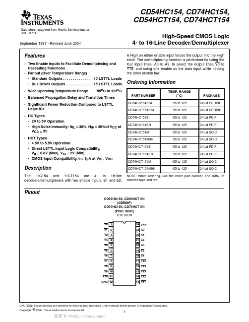
CD54HC154, CD74HC154, CD54HCT154, CD74HCT154
Functional Diagram
A0 23 A1 22 A2 21
20 A3
E1 18 E2 19
1 Y0
2 Y1
3 Y2
4 Y3
5 Y4
6 Y5
7 Y6
8 Y7
[ /Title (CD74 HC154 , CD74 HCT15 4) /Subject (High Speed CMOS Logic 4-to-16 Line Decod er/Dem
Features
• Two Enable Inputs to Facilitate Demultiplexing and Cascading Functions
Data sheet acquired from Harris Semiconductor SCHS152D
September 1997 - Revised June 2004
CD54HC154, CD74HC154, CD54HCT154, CD74HCT154
High-Speed CMOS Logic 4- to 16-Line Decoder/Demultiplexer
CD74HC163中文资料

14 Q0
13 Q1
12 Q2
11 Q3
15 TC
OPERATING MODE Reset (Clear) Parallel Load
Count Inhibit
MODE SELECT - FUNCTION TABLE FOR CD74HC/HCT161
INPUTS
MR
CP
PE
TE
SPE
Pn
L
X
X
X
X
• Wide Operating Temperature Range . . . -55oC to 125oC
• Balanced Propagation Delay and Transition Times
• Significant Power Reduction Compared to LSTTL Logic ICs
Pinout
CD74HC161, CD74HCT161, CD74HC163, CD74HCT163 (PDIP, SOIC) TOP VIEW
CD74HCT161M
-55 to 125
16 Ld SOIC M16.15
CD74HCT163E
-55 to 125
16 Ld PDIP E16.3
CD74HCT163M
16 Ld PDIP E16.3
CD74HC163M
-55 to 125
16 Ld SOIC M16.15
CD74HCT161E
-55 to 125
16 Ld PDIP E16.3
The look-ahead carry feature simplifies serial cascading of the counters. Both count enable inputs (PE and TE) must be high to count. The TE input is gated with the Q outputs of all four stages so that at the maximum count the terminal count (TC) output goes high for one clock period. This TC pulse is used to enable the next cascaded stage.
74HC245中文资料_数据手册_参数

74HC245八路巴士TRANCEIVER;三态 14.修订历史表13:修订记录文档ID发布日期数据表状态更改注意文档.数取代版本 74HC_HCT245_3 20050131产品数据表 - 9397 750 14502 74HC_HCT245_CNV_2莫迪科幻阳离子: ? 本数据表的格式经过重新设计以符 合新的演示文稿和飞利浦半导体的信息标准 ?第4节“订购信息”,第6节“固定信息”和第13节“包装大纲“修改为包含DHVQFN20 包. 74HC_HCT245_CNV_2 19930930产品SPECI FI CATION 9397 750 14502 ? 74HC245 NV 2005.保留所有权利. 74HC245产品数据表 2005年1月3日至31日 13的22飞利浦半导体 74HC245; 74HCT245八 路巴士TRANCEIVER;三态 12.波形测量点在表11中给出. V OL 和V OH 是输出负载时发生的典型电压输出下降.图5.输入(AN,BN) 输出(BN,AN)传播延迟和输出转换时间测量点在表11中给出. V OL 和V OH 是输出负载时发生的典型电压输出下降.图6. 3态输出 启用和禁用时间表11:测量点类型输入产量 74HC245保留所有权利.产品数据表 2005年1月3日至3月31日 13的22飞利浦半导体 74HC245; 74HCT245八路公交车三态波形测量点在表 11中给出. V OL 和V OH 是输出负载时发生的典型电压输出降.图5.输入(An,Bn)输出(Bn,An)传播延迟和输出转换时间测量点 在表11中给出. V OL 和V OH 是输出负载时发生的典型电压输出降.图6. 3状态输出使能和禁止时间表11:测量点类型输入产量 V M V M 74HC245 0.5V CC 0.5V CC 74HCT245 1.3 V 1.3 V 001aac433 t PLH t PHL VM V M 90% 10% V M V M Bn,输出 An,Bn输入 V 我 GND V OH V OL t TLH t THL 001aac479 t PLZ t PHZ输出残输出启用 90% 10%输出启用 OE输入 V 我 V CC V OL V OH GND GND V M t PZL t PZH V M V M产量 LOW-到关关到LOW产量 74HC245输出频率; C L = pF中的输出负载电容; V CC =电源电压V; N =输入切换次数; Σ(C L ×V CC 2 ×f o )=输出和.表10:动态特 性类型74HCT245 GND = 0 V;测试电路见图7.符号参数条件敏典型马克斯单元 T amb = 25°C t PHL ,t PLH传播延迟A到Bn或Bn到安见 图5 V CC = 4.5 V - 12 22 NS V CC = 5.0 V; C L = 15pF - 10 - NS t PZH ,t PZL 3状态输出使能时间OE A或OE到Bn V CC = 4.5V; 见图6 1630ns PHZ ,t PLZ 3状态输出禁用时间OE A或OE到Bn V CC = 4.5V; 见图6 - 1630ns t THL ,t TLH输出转换时间 V CC = 4.5V; 见图5 - 五 12 NS C PD功耗电容每个收发器 V I = GND至V CC - 1.5 V [1] -30 - pF的 T amb = -40°C至+85°C t PHL ,t PLH传播延迟A到Bn或Bn到 安 V CC = 4.5V; 见图5 --28 NS t PZH ,t PZL 3状态输出使能时间OE A或OE到Bn V CC = 4.5V; 见图6 --38 NS PHZ ,t PLZ 3状态输出禁 用时间OE A或OE到Bn V CC = 4.5V; 见图6 --38 NS t THL ,t TLH输出转换时间 V CC = 4.5V; 见图5 --15 NS T amb = -40°C至+125°C t PHL ,t PLH传播延迟A到Bn或Bn到安 V CC = 4.5V; 见图5 --33 NS t PZH ,t PZL 3状态输出使能时间
74HC245详细中文资料

74HC245详细中文资料74HC245是一款高速CMOS器件,74HC2 45引脚兼容低功耗肖特基TTL(LSTTL)系列。
74HC245译码器可接受3位二进制加权地址输入(A0, A1和A2),并当使能时,提供8个互斥的低有效输出(Y0至Y7)。
74HC245特有3个使能输入端:两个低有效(E1和E2)和一个高有效(E3)。
除非E1和E2置低且E3置高,否则74HC138将保持所有输出为高。
利用这种复合使能特性,仅需4片7 4HC245芯片和1个反相器,即可轻松实现并行扩展,组合成为一个1-32(5线到32线)译码器。
任选一个低有效使能输入端作为数据输入,而把其余的使能输入端作为选通端,则74HC245亦可充当一个8输出多路分配器,未使用的使能输入端必须保持绑定在各自合适的高有效或低有效状态。
74HC245与74HC 238逻辑功能一致,只不过74HC138为反相输出。
功能CD74HC245 ,CD74HC238和CD74HCT245, CD74HCT238是高速硅栅CMO S解码器,适合内存地址解码或数据路由应用。
74HC245作用原理于高性能的存贮译码或要求传输延迟时间短的数据传输系统,在高性能存贮器系统中,用这种译码器可以提高译码系统的效率。
将快速赋能电路用于高速存贮器时,译码器的延迟时间和存贮器的赋能时间通常小于存贮器的典型存取时间,这就是说由肖特基钳位的系统译码器所引起的有效系统延迟可以忽略不计。
HC138 按照三位二进制输入码和赋能输入条件,从8 个输出端中译出一个低电平输出。
两个低电平有效的赋能输入端和一个高电平有效的赋能输入端减少了扩展所需要的外接门或倒相器,扩展成24 线译码器不需外接门;扩展成32 线译码器,只需要接一个外接倒相器。
在解调器应用中,赋能输入端可用作数据输入端。
特性复合使能输入,轻松实现扩展兼容JEDEC标准no.7A 存储器芯片译码选择的理想选择低有效互斥输出 ESD保护 HBM EIA/JESD22-A114-C超过2000 V MM EIA/JESD22-A115-A超过200 V 温度范围 -40~+85 ℃ -40~+125 ℃多路分配功能74HC245是一款高速CMOS器件,74HC245引脚兼容低功耗肖特基T TL(LSTTL)系列。
74LV241DB中文资料
元器件交易网DIP20:plastic dual in-line package; 20 leads (300 mil)SOT146-1SO20:plastic small outline package; 20 leads; body width 7.5 mm SOT163-1SSOP20:plastic shrink small outline package; 20 leads; body width 5.3 mm SOT339-1TSSOP20:plastic thin shrink small outline package; 20 leads; body width 4.4 mm SOT360-1Philips Semiconductors and Philips Electronics North America Corporation reserve the right to make changes, without notice, in the products,including circuits, standard cells, and/or software, described or contained herein in order to improve design and/or performance. Philips Semiconductors assumes no responsibility or liability for the use of any of these products, conveys no license or title under any patent, copyright,or mask work right to these products, and makes no representations or warranties that these products are free from patent, copyright, or mask work right infringement, unless otherwise specified. Applications that are described herein for any of these products are for illustrative purposes only. Philips Semiconductors makes no representation or warranty that such applications will be suitable for the specified use without further testing or modification.LIFE SUPPORT APPLICATIONS Philips Semiconductors and Philips Electronics North America Corporation Products are not designed for use in life support appliances, devices,or systems where malfunction of a Philips Semiconductors and Philips Electronics North America Corporation Product can reasonably be expected to result in a personal injury. Philips Semiconductors and Philips Electronics North America Corporation customers using or selling Philips Semiconductors and Philips Electronics North America Corporation Products for use in such applications do so at their own risk and agree to fully indemnify Philips Semiconductors and Philips Electronics North America Corporation for any damages resulting from such improper use or sale.This data sheet contains preliminary data, and supplementary data will be published at a later date. PhilipsSemiconductors reserves the right to make changes at any time without notice in order to improve designand supply the best possible product.Philips Semiconductors811 East Arques AvenueP .O. Box 3409Sunnyvale, California 94088–3409Telephone 800-234-7381DEFINITIONSData Sheet IdentificationProduct Status Definition Objective Specification Preliminary Specification Product Specification Formative or in Design Preproduction Product Full ProductionThis data sheet contains the design target or goal specifications for product development. Specificationsmay change in any manner without notice.This data sheet contains Final Specifications. Philips Semiconductors reserves the right to make changesat any time without notice, in order to improve design and supply the best possible product.© Copyright Philips Electronics North America Corporation 1998All rights reserved. Printed in U.S.A.print codeDate of release: 05-96。
74HC245中文资料,74HC245N规格书,74HC245D技术文档,DATASHEET,NXP代理商
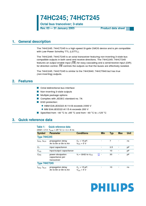
74HC245; 74HCT245
Octal bus tranceiver; 3-state
Rev. 03 — 31 January 2005
Product data sheet
1. General description
The 74HC245; 74HCT245 is a high-speed Si-gate CMOS device and is pin compatible with Low-Power Schottky TTL (LSTTL).
plastic shrink small outline package; 20 leads; body width 5.3 mm
SOT339-1
74HCT245BQ
−40 °C to +125 °C
DHVQFN20 plastic dual-in-line compatible thermal enhanced SOT764-1 very thin quad flat package no leads; 20 terminals; body 2.5 × 4.5 × 0.85 mm
x HBM EIA/JESD22-A114-B exceeds 2000 V x MM EIA/JESD22-A115-A exceeds 200 V s Specified from −40 °C to +85 °C and from −40 °C to +125 °C
3. Quick reference data
SOT163-1
74HCT245PW
−40 °C to +125 °C TSSOP20 plastic thin shrink small outline package; 20 leads; SOT360-1 body width 4.4 mm
- 1、下载文档前请自行甄别文档内容的完整性,平台不提供额外的编辑、内容补充、找答案等附加服务。
- 2、"仅部分预览"的文档,不可在线预览部分如存在完整性等问题,可反馈申请退款(可完整预览的文档不适用该条件!)。
- 3、如文档侵犯您的权益,请联系客服反馈,我们会尽快为您处理(人工客服工作时间:9:00-18:30)。
TEMP. RANGE (oC)
PACKAGE
-55 to 125
20 Ld CERDIP
-55 to 125
20 Ld CERDIP
-55 to 125
20 Ld CERDIP
-55 to 125
20 Ld CERDIP
-55 to 125
20 Ld CERDIP
-55 to 125
20 Ld PDIP
HC Types . . . . . . . . . . . . . . . . . . . . . . . . . . . . . . . . . . . . .2V to 6V HCT Types . . . . . . . . . . . . . . . . . . . . . . . . . . . . . . . . .4.5V to 5.5V DC Input or Output Voltage, VI, VO . . . . . . . . . . . . . . . . . 0V to VCC Input Rise and Fall Time 2V . . . . . . . . . . . . . . . . . . . . . . . . . . . . . . . . . . . . . . 1000ns (Max) 4.5V. . . . . . . . . . . . . . . . . . . . . . . . . . . . . . . . . . . . . . 500ns (Max) 6V . . . . . . . . . . . . . . . . . . . . . . . . . . . . . . . . . . . . . . . 400ns (Max)
DC Supply Voltage, VCC . . . . . . . . . . . . . . . . . . . . . . . . -0.5V to 7V DC Input Diode Current, IIK
For VI < -0.5V or VI > VCC + 0.5V . . . . . . . . . . . . . . . . . . . . . .±20mA DC Output Diode Current, IOK
• HC Types
- 2V to 6V Operation
- High Noise Immunity: NIL = 30%, NIH = 30% of VCC at VCC = 5V
• HCT Types
- 4.5V to 5.5V Operation
- Direct LSTTL Input Logic Compatibility, VIL= 0.8V (Max), VIH = 2V (Min)
Features
Ordering Information
• HC/HCT240 Inverting
• HC/HCT241 Non-Inverting
• HC/HCT244 Non-Inverting
•
Typical Propagation Delay = 8ns CL = 15pF, TA = 25oC for HC240
CD54/74HC244, CD54/74HCT244
High-Speed CMOS Logic
Octal Buffer/Line Drivers, Three-State
[ /Title (CD74 HC240 , CD74 HCT24 0, CD74 HC241 , CD74 HCT24 1, CD74 HC244 , CD74
CD74HC240, CD74HC241, CD74HCT241, CD74HC244, CD74HCT244 (PDIP, SOIC) CD74HCT240, (PDIP, SOIC, TSSOP)
TOP VIEW
241 240 244
241
244
240
1OE 1A0 2Y3 1A1 2Y2 1A2 2Y1 1A3 2Y0 GND
Thermal Information
Thermal Resistance (Typical, Note 1)
θJA
E (PDIP) Package . . . . . . . . . . . . . . . . . . . . . . . . . 69oC/W
M (SOIC) Package . . . . . . . . . . . . . . . . . . . . . . . . . 58oC/W
For VO < -0.5V or VO > VCC + 0.5V . . . . . . . . . . . . . . . . . . . .±20mA DC Drain Current, per Output, IO
For -0.5V < VO < VCC + 0.5V. . . . . . . . . . . . . . . . . . . . . . . . . . ±35mA DC Output Source or Sink Current per Output Pin, IO
元器件交易网
Data sheet acquired from Harris Semiconductor SCHS167E November 1997 - Revised October 2004
CD54/74HC240, CD54/74HCT240, CD74HC241, CD54/74HCT241,
1OE 1 1A0 2 2Y3 3 1A1 4 2Y2 5 1A2 6 2Y1 7 1A3 8 2Y0 9 GND 10
20 VCC VCC 19 2OE (241) 2OE (240, 244) 18 1Y0 1Y0 17 2A3 2A3 16 1Y1 1Y1 15 2A2 2A2 14 1Y2 1Y2 13 2A1 2A1 12 1Y3 1Y3 11 2A0 2A0
- CMOS Input Compatibility, Il ≤ 1µA at VOL, VOH
PART NUMBER CD54HC240F3A CD54HC244F3A CD54HCT240F3A CD54HCT241F3A CD54HCT244F3A CD74HC240E CD74HC240M CD74HC240M96 CD74HC241E CD74HC241M CD74HC241M96 CD74HC244E CD74HC244M CD74HC244M96 CD74HCT240E CD74HCT240M CD74HCT240M96
Functional Diagram
2 1A0
4 1A1
6 1A2
8 1A3
11 2A0
13 2A1
15 2A2
240
17
AND 2A3
244 241
1OE 1OE
2OE 2OE
1 19
241 AND 244 240
18 1Y0 1Y0
16 1Y1 1Y1
14 1Y2 1Y2
12 1Y3 1Y3
9 2Y0 2Y0
PW (TSSOP) Package . . . . . . . . . . . . . . . . . . . . . . 83oC/W
Maximum Junction Temperature . . . . . . . . . . . . . . . . . . . . . . . 150oC
Maximum Storage Temperature Range . . . . . . . . . .-65oC to 150oC
Maximum Lead Temperature (Soldering 10s) . . . . . . . . . . . . . 300oC
(SOIC - Lead Tips Only)
Operating Conditions
Temperature Range (TA) . . . . . . . . . . . . . . . . . . . . . -55oC to 125oC Supply Voltage Range, VCC
1
元器件交易网
CD54/74HC240, CD54/74HCT240, CD74HC241, CD54/74HCT241, CD54/74HC244, CD54/74HCT244
Pinout
CD54HC240, CD54HCT240, CD54HCT241, CD54HC244, CD54HCT244 (CERDIP)
• Wide Operating Temperature Range . . . -55oC to 125oC
• Balanced Propagation Delay and Transition Times
• Significant Power Reduction Compared to LSTTL Logic ICs
CAUTION: These devices are sensitive to electrostatic discharge. Users should follow proper IC Handling Procedures.
Copyright © 2004, Texas Instruments Incorporated
20 Ld SOIC
-55 to 125
20 Ld PDIP
-55 to 125
20 Ld SOIC
-55 to 125
20 Ld SOIC
Description
The ’HC240 and ’HCT240 are inverting three-state buffers having two active-low output enables. The CD74HC241, ’HCT241, ’HC244 and ’HCT244 are non-inverting threestate buffers that differ only in that the 241 has one activehigh and one active-low output enable, and the 244 has two active-low output enables. All three types have identical pinouts.