MUBW10-12A7中文资料
BW10红光源中文说明书

3、激光器工作时,光纤接头应处理干净,否则会影响使用效果;
4、不使用本光源时,请将防尘帽戴好以避免灰尘落入;
5、人为使用不当造成的损坏,如:摔、碰或自行拆卸不在保修范围内,维修需收取成本 费;
6、出厂日期小标签请勿撕毁,否则,本公司不提供售后服务。 五、产品参数
产品型号 工作波长 发光器件 谱宽(20℃) 光纤类别 测试接口 输出功率(mW) 工作温度(℃) 存储温度(℃) 外壳材料
2、将笔尾与笔身连接装好,打开防尘帽,按控制开关一次,观察光接口有红光光出来,
同时指示发光管点亮;(注意不要眼睛正对光接口,以免损伤眼睛)。
3、再按控制开关一次,观察出光变为脉冲模式,指示发光管与出光同步脉冲;(脉冲频率
在 0.5~2 赫兹)。
4、再按控制开关一次,光源关闭,无光输出,同时指示发光管熄灭;(开关模式为:连续
1、型号:BW-10-A/T/G-X
2、材质:A-铝合金,T-铜合金,G-不锈钢
3、输出功率(mW):X=5、10、20、30
BW-10-A
BW-10-T
BW-10-G
-脉冲-关闭-连续的循环模式)。
5、检测时将被测光纤插入光接口,同时按控制开关,选择输出光源工作模式(连续或脉
冲)。
6、使用完毕,将防尘帽盖起,长时间不使用,请将电池取出,以免电池腐烂,损坏光源。
四、维护与注意事项
1、激光有害,尤其要注意保护眼睛,激光器工作时,避免激光直射眼睛;
2、一般情况下,温度越高,激光器寿命越短,使用时尽量避免高温工作环境;
适用光纤:SM、MM
检测距离:5公里~20公里
电源:2节1.5V电池
电源连续工作时间:≥10h
工作温度:-10~+60℃(不结露)
变频器驱动电阻
文件名称 文件编号
IGBT 门极驱动电阻参数表 IV-TSP-000954
页 数: 第 2 页 共 18 页
文件修订信息记录表
序号
1 2
3 4
版本
A B
C
更改单号
/ /
/
修订原因及修订内容
新拟制
1、 表 2 中新增 GD800 系列的内容。 2、 表 5 中新增高压系列斯达模块和 ME4 模块。 3、 表 3 中将中压 660V 上的 BSM75GB170DN2、
备注: 1、 BOM清单中的门极驱动电阻与本表有不同者,以本表数据为准。
文件名称 文件编号
IGBT 门极驱动电阻参数表 IV-TSP-000954
页 数: 第 4 页 共 18 页
表2 380V系列变频器产品IGBT门极驱动电阻表
机型系列 光板型号
CH系列
1160-A
1160-AS 1160-AT 1160-AF
V23990-P549-A01-PM
IKW08T120
IKW15N120T2
1.5kW GD10PJK120L1S
门极驱动电阻参数 Ω
R41=R43=R45=R47=R50=R53=R57=150/1206
R41=R43=R45=R47=R50=R53=R57=200/1206 R41=R43=R45=R47=R50=R53=R57=68/1206 R41=R43=R45=R47=R50=R53=R57=100/1206
7MBR25SA120
5.5kW
FP40R12KE3 FP40R12KT3 GD40PIT120C5S MUBW35-12A7 MUBW35-12E7
V23990-P580-A-PM
威世二极管规格书

SMBJ5.0 thru SMBJ188CAVishay General SemiconductorDocument Number: 88392For technical questions within your region, please contact one of the following:Surface Mount T RANS Z ORB ® Transient Voltage SuppressorsFEATURES•Low profile package•Ideal for automated placement •Glass passivated chip junction••cycle): 0.01 %•Excellent clamping capability •Very fast response time•Low incremental surge resistance•Meets MSL level 1, per J-STD-020, LF maximum peak of 260 °C•Solder dip 260 °C, 40 s •Component in accordance to RoHS 2002/95/EC and WEEE 2002/96/EC TYPICAL APPLICATIONSUse in sensitive electronics protection against voltage transients induced by inductive load switching and lighting on ICs, MOSFET, signal lines of sensor units for consumer, computer, industrial, automotive and telecommunication.MECHANICAL DATA Case: DO-214AA (SMBJ)Molding compound meets UL 94 V-0 flammabilityratingBase P/N-E3 - RoHS compliant, commercial grade Base P/NHE3 - RoHS compliant, high reliability/automotive grade (AEC Q101 qualified)Terminals: Matte tin plated leads, solderable per J-STD-002 and JESD22-B102E3 suffix meets JESD 201 class 1A whisker test, HE3suffix meets JESD 201 class 2 whisker testPolarity: For uni-directional types the band denotes cathode end, no marking on bi-directional typesDEVICES FOR BI-DIRECTION APPLICATIONS For bi-directional devices use C or CA suffix (e.g. SMBJ10CA).Electrical characteristics apply in both directions.PRIMARY CHARACTERISTICSV WM 5.0 V to 188 VP PPM600 W I FSM (uni-directional only)100 A T J max.150 °CDO-214AA (SMB J-Bend)Notes:(1) Non-repetitive current pulse, per Fig. 3 and derated above T A = 25 °C per Fig. 2(2) Mounted on 0.2 x 0.2" (5.0 x 5.0 mm) copper pads to each terminalMAXIMUM RATINGS (T A = 25°C unless otherwise noted)PARAMETERSYMBOL VALUE UNIT Peak pulse power dissipation with a 10/1000 µs waveform (1)(2) (Fig. 1) P PPM 600 W Peak pulse current with a 10/1000 µs waveform (1)I PPM See next table A Peak forward surge current 8.3 ms single half sine-wave uni-directional only (2) I FSM 100 AOperating junction and storage temperature range T J , T STG- 55 to + 150°CSMBJ5.0 thru SMBJ188CAVishay General Semiconductor For technical questions within your region, please contact one of the following:Document Number: 88392ELECTRICAL CHARACTERISTICS (T A = 25°C unless otherwise noted)DEVICE TYPE MODIFIED“J” BEND LEADDEVICE MARKINGCODE BREAKDOWN VOLTAGE V BR AT I T (1)(V) TEST CURRENTI T (mA) STAND-OFF VOLTAGE V WM (V)MAXIMUM REVERSE LEAKAGE AT V WM I D (µA) (3)MAXIMUM PEAK PULSE SURGE CURRENT I PPM (A)(2)MAXIMUM CLAMPING VOLTAGE AT I PPMV C (V)UNIBIMIN.MAX.(+)SMBJ5.0 KD KD 6.40 7.82 10 5.0 800 62.5 9.6(+)SMBJ5.0A (5)KE KE 6.40 7.07 10 5.0 800 65.2 9.2(+)SMBJ6.0 KF KF 6.67 8.15 10 6.0 800 52.6 11.4 (+)SMBJ6.0A KG KG 6.67 7.37 10 6.0 800 58.3 10.3 (+)SMBJ6.5 KH AH 7.22 8.82 10 6.5 500 48.8 12.3 (+)SMBJ6.5A KK AK 7.22 7.98 10 6.5 500 53.6 11.2 (+)SMBJ7.0 KL KL 7.78 9.51 10 7.0 200 45.1 13.3 (+)SMBJ7.0A KM KM 7.78 8.60 10 7.0 200 50.0 12.0 (+)SMBJ7.5 KN AN 8.33 10.2 1.0 7.5 100 42.0 14.3 (+)SMBJ7.5A KP AP 8.33 9.21 1.0 7.5 100 46.5 12.9 (+)SMBJ8.0 KQ AQ 8.89 10.9 1.0 8.0 50 40.0 15.0 (+)SMBJ8.0A KR AR 8.89 9.83 1.0 8.0 50 44.1 13.6 (+)SMBJ8.5 KS AS 9.44 11.5 1.0 8.5 20 37.7 15.9 (+)SMBJ8.5A KT AT 9.44 10.4 1.0 8.5 20 41.7 14.4 (+)SMBJ9.0 KU AU 10.0 12.2 1.0 9.0 10 35.5 16.9 (+)SMBJ9.0A KV AV 10.0 11.1 1.0 9.0 10 39.0 15.4 (+)SMBJ10 KW AW 11.1 13.6 1.0 10 5.0 31.9 18.8 (+)SMBJ10A KX AX 11.1 12.3 1.0 10 5.0 35.3 17.0 (+)SMBJ11 KY KY 12.2 14.9 1.0 11 5.0 29.9 20.1 (+)SMBJ11A KZ KZ 12.2 13.5 1.0 11 5.0 33.0 18.2 (+)SMBJ12 LD BD 13.3 16.3 1.0 12 5.0 27.3 22.0 (+)SMBJ12A LE BE 13.3 14.7 1.0 12 5.0 30.2 19.9 (+)SMBJ13 LF LF 14.4 17.6 1.0 13 1.0 25.2 23.8 (+)SMBJ13A LG LG 14.4 15.9 1.0 13 1.0 27.9 21.5 (+)SMBJ14 LH BH 15.6 19.1 1.0 14 1.0 23.3 25.8 (+)SMBJ14A LK BK 15.6 17.2 1.0 14 1.0 25.9 23.2 (+)SMBJ15 LL BL 16.7 20.4 1.0 15 1.0 22.3 26.9 (+)SMBJ15A LM BM 16.7 18.5 1.0 15 1.0 24.6 24.4 (+)SMBJ16 LN LN 17.8 21.8 1.0 16 1.0 20.8 28.8 (+)SMBJ16A LP LM 17.8 19.7 1.0 16 1.0 23.1 26.0 (+)SMBJ17 LQ LQ 18.9 23.1 1.0 17 1.0 19.7 30.5 (+)SMBJ17A LR LR 18.9 20.9 1.0 17 1.0 21.7 27.6 (+)SMBJ18 LS BS 20.0 24.4 1.0 18 1.0 18.6 32.2 (+)SMBJ18A LT BT 20.0 22.1 1.0 18 1.0 20.5 29.2 (+)SMBJ20 LU LU 22.2 27.1 1.0 20 1.0 16.8 35.8 (+)SMBJ20A LV LV 22.2 24.5 1.0 20 1.0 18.5 32.4 (+)SMBJ22 LW BW 24.4 29.8 1.0 22 1.0 15.2 39.4 (+)SMBJ22A LX BX 24.4 26.9 1.0 22 1.0 16.9 35.5 (+)SMBJ24 L Y BY 26.7 32.6 1.0 24 1.0 14.0 43.0 (+)SMBJ24A LZ BZ 26.7 29.5 1.0 24 1.0 15.4 38.9 (+)SMBJ26 MD CD 28.9 35.3 1.0 26 1.0 12.9 46.6 (+)SMBJ26A ME CE 28.9 31.9 1.0 26 1.0 14.3 42.1 (+)SMBJ28 MF MF 31.1 38.0 1.0 28 1.0 12.0 50.0 (+)SMBJ28A MG MG 31.1 34.4 1.0 28 1.0 13.2 45.4 (+)SMBJ30 MH CH 33.3 40.7 1.0 30 1.0 11.2 53.5 (+)SMBJ30A MK CK 33.3 36.8 1.0 30 1.0 12.4 48.4 (+)SMBJ33 ML CL 36.7 44.9 1.0 33 1.0 10.2 59.0 (+)SMBJ33A MM CM 36.7 40.6 1.0 33 1.0 11.3 53.3 (+)SMBJ36 MN CN 40.0 48.9 1.0 36 1.0 9.3 64.3 (+)SMBJ36A MP CP 40.0 44.2 1.0 36 1.0 10.3 58.1 (+)SMBJ40 MQ CQ 44.4 54.3 1.0 40 1.0 8.4 71.4 (+)SMBJ40A MR CR 44.4 49.1 1.0 40 1.0 9.3 64.5SMBJ5.0 thru SMBJ188CAVishay General SemiconductorDocument Number: 88392For technical questions within your region, please contact one of the following:Notes:(1)Pulse test: tp ≤ 50 ms(2)Surge current waveform per Fig. 3 and derate per Fig. 2(3)For bi-directional types having V WM of 10 V and less, the I D limit is doubled (4)All terms and symbols are consistent with ANSI/IEEE C62.35(5)For the bi-directional SMBG/SMBJ5.0CA, the maximum V BR is 7.25 V (6)V F = 3.5 V at I F = 50 A (uni-directional only)(+)Underwriters laboratory recognition for the classification of protectors (QVGQ2) under the UL standard for safety 497B and file number E136766 for both uni-directional and bi-directional devices(+)SMBJ43 MS CS 47.8 58.4 1.0 43 1.0 7.8 76.7(+)SMBJ43A MT CT 47.8 52.8 1.043 1.0 8.6 69.4(+)SMBJ45 MU MU 50.0 61.1 1.0 45 1.0 7.5 80.3 (+)SMBJ45A MV MV 50.0 55.3 1.0 45 1.0 8.3 72.7 (+)SMBJ48 MW MW 53.3 65.1 1.0 48 1.0 7.0 85.5 (+)SMBJ48A MX MX 53.3 58.9 1.0 48 1.0 7.8 77.4 (+)SMBJ51 MY MY 56.7 69.3 1.0 51 1.0 6.6 91.1 (+)SMBJ51A MZ MZ 56.7 62.7 1.0 51 1.0 7.3 82.4 (+)SMBJ54 ND ND 60.0 73.3 1.0 54 1.0 6.2 96.3 (+)SMBJ54A NE NE 60.0 66.3 1.0 54 1.0 6.9 87.1 (+)SMBJ58 NF NF 64.4 78.7 1.0 58 1.0 5.8 103 (+)SMBJ58A NG NG 64.4 71.2 1.0 58 1.0 6.4 93.6 (+)SMBJ60 NH NH 66.7 81.5 1.0 60 1.0 5.6 107 (+)SMBJ60A NK NK 66.7 73.7 1.0 60 1.0 6.2 96.8 (+)SMBJ64 NL NL 71.1 86.9 1.0 64 1.0 5.3 114 (+)SMBJ64A NM NM 71.1 78.6 1.0 64 1.0 5.8 103 (+)SMBJ70 NN NN 77.8 95.1 1.0 70 1.0 4.8 125 (+)SMBJ70A NP NP 77.8 86.0 1.0 70 1.0 5.3 113 (+)SMBJ75 NQ NQ 83.3 102 1.0 75 1.0 4.5 134 (+)SMBJ75A NR NR 83.3 92.1 1.0 75 1.0 5.0 121 (+)SMBJ78 NS NS 86.7 106 1.0 78 1.0 4.3 139 (+)SMBJ78A NT NT 86.7 95.8 1.0 78 1.0 4.8 126 (+)SMBJ85 NU NU 94.4 115 1.0 85 1.0 4.0 151 (+)SMBJ85A NV NV 94.4 104 1.0 85 1.0 4.4 137 (+)SMBJ90 NW NW 100 122 1.0 90 1.0 3.8 160 (+)SMBJ90A NX NX 100 111 1.0 90 1.0 4.1 146 (+)SMBJ100 NY NY 111 136 1.0 100 1.0 3.4 179 (+)SMBJ100A NZ NZ 111 123 1.0 100 1.0 3.7 162 (+)SMBJ110 PD PD 122 149 1.0 110 1.0 3.1 196 (+)SMBJ110A PE PE 122 135 1.0 110 1.0 3.4 177 (+)SMBJ120 PF PF 133 163 1.0 120 1.0 2.8 214 (+)SMBJ120A PG PG 133 147 1.0 120 1.0 3.1 193 (+)SMBJ130 PH PH 144 176 1.0 130 1.0 2.6 231 (+)SMBJ130A PK PK 144 159 1.0 130 1.0 2.9 209 (+)SMBJ150 PL PL 167 204 1.0 150 1.0 2.2 268 (+)SMBJ150A PM PM 167 185 1.0 150 1.0 2.5 243 (+)SMBJ160 PN PN 178 218 1.0 160 1.0 2.1 287 (+)SMBJ160A PP PP 178 197 1.0 160 1.0 2.3 259 (+)SMBJ170 PQ PQ 189 231 1.0 170 1.0 2.0 304 (+)SMBJ170A PR PR 189 209 1.0 170 1.0 2.2 275 SMBJ188 PT PT 209 255 1.0 188 1.0 1.7 344 SMBJ188A PS PS 209 231 1.0 188 1.0 2.0 328ELECTRICAL CHARACTERISTICS (T A = 25°C unless otherwise noted)DEVICE TYPE MODIFIED“J” BEND LEADDEVICE MARKINGCODE BREAKDOWN VOLTAGE V BR AT I T (1)(V) TEST CURRENTI T (mA) STAND-OFF VOLTAGE V WM (V)MAXIMUM REVERSE LEAKAGE AT V WM I D (µA) (3)MAXIMUM PEAK PULSE SURGE CURRENT I PPM (A) (2)MAXIMUM CLAMPING VOLTAGE AT I PPMV C (V)UNIBIMIN.MAX.SMBJ5.0 thru SMBJ188CAVishay General Semiconductor For technical questions within your region, please contact one of the following:Document Number: 88392Note:(1) Mounted on minimum recommended pad layoutNote:(1) Automotive grade AEC Q101 qualifiedRATINGS AND CHARACTERISTICS CURVES (T A = 25 °C unless otherwise noted)THERMAL CHARACTERISTICS (T A = 25°C unless otherwise noted)PARAMETERSYMBOL VALUEUNITTypical thermal resistance, junction to ambient (1)R θJA 100 °C/WTypical thermal resistance, junction to lead R θJL20 °C/WORDERING INFORMATION (Example)PREFERRED P/N UNIT WEIGHT (g)PREFERRED PACKAGE CODEBASE QUANTITYDELIVERY MODESMBJ5.0A-E3/520.096527507" diameter plastic tape and reel SMBJ5.0A-E3/5B 0.0965B 320013" diameter plastic tape and reel SMBJ5.0AHE3/52 (1)0.096527507" diameter plastic tape and reel SMBJ5.0AHE3/5B (1)0.0965B320013" diameter plastic tape and reelFigure 1. Peak Pulse Power Rating Curve Figure 2. Pulse Power or Current vs. Initial Junction TemperatureFigure 3. Pulse WaveformFigure 4. Typical Junction CapacitanceSMBJ5.0 thru SMBJ188CAVishay General SemiconductorDocument Number: 88392For technical questions within your region, please contact one of the following:PACKAGE OUTLINE DIMENSIONS in inches (millimeters)Figure 5. Typical Transient Thermal ImpedanceFigure6. Maximum Non-Repetitive Peak Forward Surge CurrentDisclaimer Legal Disclaimer NoticeVishayALL PRODUCT, PRODUCT SPECIFICATIONS AND DATA ARE SUBJECT TO CHANGE WITHOUT NOTICE TO IMPROV E RELIABILITY, FUNCTION OR DESIGN OR OTHERWISE.Vishay Intertechnology, Inc., its affiliates, agents, and employees, and all persons acting on its or their behalf (collectively,“Vishay”), disclaim any and all liability for any errors, inaccuracies or incompleteness contained in any datasheet or in any other disclosure relating to any product.Vishay makes no warranty, representation or guarantee regarding the suitability of the products for any particular purpose or the continuing production of any product. To the maximum extent permitted by applicable law, Vishay disclaims (i) any and all liability arising out of the application or use of any product, (ii) any and all liability, including without limitation special, consequential or incidental damages, and (iii) any and all implied warranties, including warranties of fitness for particular purpose, non-infringement and merchantability.Statements regarding the suitability of products for certain types of applications are based on Vishay’s knowledge of typical requirements that are often placed on Vishay products in generic applications. Such statements are not binding statements about the suitability of products for a particular application. It is the customer’s responsibility to validate that a particular product with the properties described in the product specification is suitable for use in a particular application. Parameters provided in datasheets and/or specifications may vary in different applications and performance may vary over time. All operating parameters, including typical parameters, must be validated for each customer application by the customer’s technical experts. Product specifications do not expand or otherwise modify V ishay’s terms and conditions of purchase, including but not limited to the warranty expressed therein.Except as expressly indicated in writing, Vishay products are not designed for use in medical, life-saving, or life-sustaining applications or for any other application in which the failure of the Vishay product could result in personal injury or death. Customers using or selling Vishay products not expressly indicated for use in such applications do so at their own risk and agree to fully indemnify and hold Vishay and its distributors harmless from and against any and all claims, liabilities, expenses and damages arising or resulting in connection with such use or sale, including attorneys fees, even if such claim alleges that Vishay or its distributor was negligent regarding the design or manufacture of the part. Please contact authorized Vishay personnel to obtain written terms and conditions regarding products designed for such applications.No license, express or implied, by estoppel or otherwise, to any intellectual property rights is granted by this document or by any conduct of Vishay. Product names and markings noted herein may be trademarks of their respective owners.Document Number: 91000 。
Agilent 10705A单路光互ferometer和Agilent 10704A反射器说明书

7BAgilent10705A Single Beam Interferometer and Agilent10704A RetroreflectorChapter 7B Agilent10705A Single Beam Interferometer andAgilent10704A RetroreflectorDescriptionDescriptionThe Agilent10705A Single Beam Interferometer (shown inFigure7B-1) is intended for use in low-mass or limited-space applications. This Interferometer is designed for use with theAgilent10704A Retroreflector (shown in Figure7B-1); a special option (C01-10705A, described later in this subchapter) provides anAgilent10705A interferometer that can be used with plane mirrors or highly reflective surfaces.The single beam interferometer is called that because the outgoing and returning beams are superimposed on each other, giving the appearance of only one beam traveling between the interferometer and the retroreflector.Functionally, this interferometer operates like a linear interferometer, but is preferred when space for optics and beam paths is limited.The Agilent10704A Retroreflector is a cube corner, but is considerably smaller and lighter than the Agilent10703A Retroreflector.Figure7B-1. Agilent 10705A Single Beam Interferometer and Agilent 10704A Retroreflector7B-2User’s ManualChapter 7B Agilent10705A Single Beam Interferometer andAgilent10704A RetroreflectorDescriptionWhen using a single-beam interferometer, the receiver is usually mounted perpendicular to the measurement beam, and the interferometer held stationary. An optical schematic diagram of this interferometer is shown in Figure7B-2.Figure7B-2. Single Beam Interferometer — laser beam pathLaser beam pathA polarizing beam-splitter reflects fB to the reference cube corner and transmits f A to the Agilent10704A Retroreflector (Figure7B-2). The return path is superimposes on the outgoing path. Since both beams leaving the beam-splitter pass through a quarter-wave plate, the returning polarizations are rotated through 90°. This causes f B to be transmitted and f A ±∆f to be reflected so that they are directed coaxially to the receiver along a path perpendicular to the input beam. Rotating the interferometer 90° switches which optical frequency is in the measurement path, and thus changes the direction sense.User’s Manual7B-3Chapter 7B Agilent10705A Single Beam Interferometer andAgilent10704A RetroreflectorDescriptionDifferential measurementsA differential measurement is one in which both the reference beam and the measurement beam travel to external reflectors outside the interferometer housing. This allows measurement of the relative positions of the two external mirrors, either or both of which may be moving. Viewed another way, this allows measuring the motion of one reflector relative to a reference datum elsewhere in the machine, external to the interferometer itself. This is unlike the typical interferometer configuration because usually the reference beam path length does not change; in differential configurations, it can.Take care during design and layout of a differential measurement to avoid introduction of alignment errors, thermal or mechanical instabilities, and potential deadpath problems. Both reflectors (reference and measurement) should be of the same type (cube corner or plane mirror); this minimizes thermal drift problems with ambient temperature changes.To use an Agilent10705A Interferometer in a differential measurement configuration, the reference cube corner can simply be detached from the interferometer housing and attached to the reference surface of interest. This is shown, using an Agilent10702A Interferometer for the example, in Figure7A-7. Be aware that all installation and alignment requirements for the measurement reflector now apply also to the reference reflector.Plane mirror measurementsThe special option C01-10705A interferometer is an Agilent10705A interferometer specially modified to allow its use with plane mirrors or highly reflective surfaces. The C01-10705A modification removes one quarter-wave plate, resulting in an optical configuration similar to that of the Agilent10706A Plane Mirror Interferometer (described in subchapter7C of this manual); this configuration requires oneAgilent10704A retroreflector. The C01-10705A interferometer’s receiver signal is separated by an Agilent10700A or Agilent10701A Beam Splitter.Typical measurement mirror alignment requirements for theC01-10705A (as a function of distance) are the same as those for the Agilent10706A Plane Mirror Interferometer. Agilent10706A interferometer specifications are given in subchapter7C of this manual.7B-4User’s ManualChapter 7B Agilent10705A Single Beam Interferometer andAgilent10704A RetroreflectorSpecial ConsiderationsSpecial ConsiderationsEffect of optics on measurement direction senseThe orientation and configuration of the interferometer affects the measurement direction sense. The direction sense depends on which frequency is in the measurement path of the interferometer. For example, if f1 (lower frequency) is in the measurement path and f2 (higher frequency) is in the reference path and the optics are moving away from each other, the fringe counts will be INCREASING. Interchanging f1 and f2 (perhaps by rotating the interferometer 90°, the measurement direction sense will change. This rotation causes switching of frequencies in the measurement path.Configuration effectsThe Agilent10705A interferometer can be configured to turn the beam at right angles. Be aware that doing this will cause the measurement direction sense to be changed because the measurement reference paths are exchanged.MountingAdjustable mountsAgilent10710B Adjustable Mount provides a convenient means of mounting, aligning, and securely locking in position, the Agilent 10705A interferometer. Since the mount allows some tilt and yaw adjustment, the need for custom fixturing is minimized. This mount allows the optic mounted on it to be rotated about its optical centerline, simplifying installation.Chapter4. “System Installation and Alignment” in this manual shows how to install an optic in various orientations, using an adjustable mount.FastenersThe Agilent10706A interferometer is designed to be used with an Agilent10710B Adjustable Mount, and is supplied with English mounting hardwareUser’s Manual7B-5Chapter 7B Agilent 10705A Single Beam Interferometer andAgilent 10704A Retroreflector Installation7B-6User ’s ManualInstallationPre-installation checklistIn addition to reading chapters 2 through 4, and Chapter 15, “Accuracyand Repeatability,” complete the following items before installing alaser positioning system into any application.Complete Beam Path Loss Calculation (see “Calculation of signalloss ” in Chapter 3, “System Design Considerations,“ of this manual).Determine the direction sense for each axis, based on theorientation of the laser head, beam-directing optic, andinterferometer. Enter the direction sense for each axis into themeasurement system electronics. (See Chapter 5, “Laser Heads,”Chapter 14, “Principles of Operation,” and Chapter 15, “Accuracyand Repeatability,” in this manual.Provide for aligning the optics, laser head, and receiver(s) on themachine. (Ideally, you want to be able to translate beam in twodirections and rotate beam in two directions for each interferometerinput. This typically takes two adjustment optics with properorientations.)Be sure to allow for transmitted beam offset of beam splitters(Agilent 10700A and Agilent 10701A) in your design. (See the offsetspecifications under the “Specifications ” heading at the end of thissubchapter.)Refer to Chapter 4, “System Installation and Alignment,” in thismanual for installation instructions.Chapter 7B Agilent 10705A Single Beam Interferometer andAgilent 10704A Retroreflector Specifications and CharacteristicsUser ’s Manual 7B-7AlignmentAlignment aidsAlignment aids for these interferometers are listed in Chapter 4,“System Installation and Alignment ” and Chapter 9, “Accessories,” ofthis manual.ProcedureRefer to Chapter 4, “System Installation and Alignment ” in this manual for alignment instructions.Specifications and CharacteristicsSpecifications describe the device ’s warranted performance.Supplemental characteristics (indicated by TYPICAL or NOMINAL)are intended to provide non-warranted performance information usefulin applying the device.The basic optical resolution using a linear interferometer is one halfwavelength (0.316micron, 12.26microinches).Using electronic resolution extension, the system resolution isincreased significantly. Depending on the system, an additionalresolution extension factor of 32 (for Agilent 10885A and 10895A) or256 (for Agilent 10897B and 10898A) is usually available.NOTE The system resolution 1 is based on using 32X electronic resolutionextension. This is available with the Agilent 10885A andAgilent 10895A electronics.The system resolution 2 is based on using 256X electronic resolutionextension. This is available with the Agilent 10897B andAgilent 10898A electronics.InterferometerFundamental Optical Resolution System Resolution 1(see NOTE)System Resolution 2(see NOTE)Agilent 10705A λ/2 (316.5nm, 12.5µin)λ/64 (10.0nm, 0.4µin)λ/512 (1.2nm, 0.047µin)Chapter 7B Agilent10705A Single Beam Interferometer andAgilent10704A RetroreflectorSpecifications and CharacteristicsAgilent 10705A Single Beam InterferometerSpecificationsDimensions: see figure belowWeight: 85.5grams (3.0ounces)Materials Used:Housing: Stainless Steel (416)Apertures: Plastic (Nylon)Optics: Optical Grade GlassAdhesives: Low Volatility (Vacuum Grade)Maximum Transmitted Beam Deviation: ± 30 arc-minutesOptical Efficiency (including Agilent10703A Reflector):Typical: 62%Worst Case: 59%Fundamental Optical Resolution: λ/2Non-linearity Error: <4.2nm (0.17µin)456mm(0.77) TypFigure7B-3. Agilent 10705A Single Beam Interferometer — dimensions 7B-8User’s ManualChapter 7B Agilent 10705A Single Beam Interferometer andAgilent 10704A Retroreflector Specifications and CharacteristicsUser ’s Manual 7B-9Agilent 10704A Retroreflector SpecificationsFigure 7B-4. Agilent 10704A Retroreflector — dimensionsAgilent 10713C 1/2-Inch Cube Corner SpecificationsFigure 7B-5. Agilent 10713C 1/2-Inch Cube Corner, no housing — dimensionsDimensions: see figure belowWeight: 10.5grams (0.37ounce)Materials Used:Housing: Stainless Steel (416)Optics: Optical Grade GlassAdhesives: Low Volatility (Vacuum Grade)Dimensions: see figure belowWeight: 1.4grams (0.05ounce)Nodal Point Depth: 6.33 mm (0.248 inch)2.5 mm(0.10)14.3 mm(0.56)19.5 mm (0.77)B ol t C i r c l e10.2 mm A p e r t u r e(0.40 D i a )2.5 mm(0.10)20.5 mm(0.81 D i a )15.2 mm (0.60 D i a )(0.375 )(0.500 D i a )+ 0.010-0.000+ 0.000- 0.020(0.450 D i a m in .C l ea r A p e r t u r e )11.43 mm12.70 mm + 0.25- 0.009.53 mm+ 000.-510.Chapter 7B Agilent10705A Single Beam Interferometer andAgilent10704A RetroreflectorSpecifications and CharacteristicsAgilent 10713D 1/4-Inch Cube Corner Specifications Dimensions: see figure belowWeight: 0.2grams (0.007ounce)Nodal Point Depth: 3.14 mm (0.123 inch)6.35± 0.2mm D i a.(0.250± 0.008in D i a.)5.71mm(0.225D i a m in.C l ea r A p e r t u r e)4.75±0.25mm(0.187± 0.010)Figure7B-6. Agilent 10713D Cube Corner, no housing — dimensionsProduct specifications and descriptions in thisdocument subject to change without notice.Copyright (C) 2002 Agilent TechnologiesPrinted in U.S.A. 07/02This is a chapter from the manual titled:Laser and Optics User's ManualFor complete manual, order:Paper version: p/n 05517-90045CD version: p/n 05517-90063This chapter is p/n 05517-901097B-10User’s Manual。
Murata LQW03AW_00系列芯片电容器(芯片导纳)参考规格书说明书
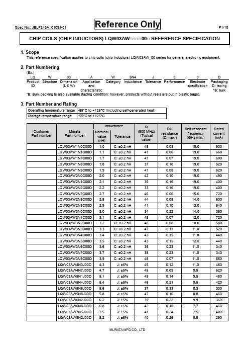
CHIP COILS (CHIP INDUCTORS) LQW03AW□□□□00□ REFERENCE SPECIFICATION1. ScopeThis reference specification applies to chip coils (chip inductors) LQW03AW_00 series for general electronic equipment.2. Part Numbering(Ex.)LQ W 03 A W 5N4 J 0 0 DProductID Structure Dimension(L × W)ApplicationandcharacteristicCategory Inductance Tolerance Performance ElectrodespecificationPackagingD: taping*B: bulk*B: Bulk packing is also available (taping condition: however, products without reels are put in plastic bags).3. Part Number and RatingOperating temperature range -55°C to +125°C (including self-generated heat)Storage temperature range -55°C to +125°CCustomer Part numberMurataPart numberInductance Q(900 MHz)(Typicalvalue)DCresistance(Ω max.)Self-resonantfrequency(GHz min.)Ratedcurrent(mA) Nominalvalue(nH)ToleranceLQW03AW1N0C00D1.0C:±0.2nH 48 0.03 19.0 900 LQW03AW1N1C00D1.1C:±0.2nH 41 0.06 19.0 660 LQW03AW1N7C00D1.7C:±0.2nH 41 0.07 19.0 600 LQW03AW1N8C00D1.8C:±0.2nH 37 0.10 19.0 520 LQW03AW1N9C00D1.9C:±0.2nH 41 0.08 19.0 620 LQW03AW2N0C00D2.0C:±0.2nH 42 0.10 19.0 490 LQW03AW2N1C00D2.1C:±0.2nH 35 0.16 19.0 400 LQW03AW2N2C00D2.2C:±0.2nH 33 0.16 19.0 400 LQW03AW2N7C00D2.7C:±0.2nH 46 0.06 15.0 720 LQW03AW2N8C00D2.8C:±0.2nH 44 0.08 14.0 600 LQW03AW2N9C00D2.9C:±0.2nH 41 0.10 13.0 540 LQW03AW3N0C00D3.0C:±0.2nH 34 0.22 14.0 350 LQW03AW3N1C00D3.1C:±0.2nH 48 0.07 12.0 720 LQW03AW3N2C00D3.2C:±0.2nH 48 0.08 10.0 580 LQW03AW3N3C00D3.3C:±0.2nH 47 0.11 11.0 520 LQW03AW3N4C00D3.4C:±0.2nH 43 0.15 11.0 440 LQW03AW3N5C00D3.5C:±0.2nH 43 0.15 12.0 440 LQW03AW3N6C00D3.6C:±0.2nH 36 0.23 11.0 340 LQW03AW3N7C00D3.7C:±0.2nH 38 0.23 11.0 340 LQW03AW3N9C00D3.9C:±0.2nH 48 0.07 11.0 650 LQW03AW4N3J00D4.3 J:±5% 45 0.12 11.0 480 LQW03AW4N7J00D4.7 J:±5% 45 0.09 9.5 620 LQW03AW5N1J00D5.1 J:±5% 45 0.14 9.5 480 LQW03AW5N4J00D5.4 J:±5% 46 0.21 9.5 420 LQW03AW5N6J00D5.6 J:±5% 37 0.33 8.3 330 LQW03AW5N8J00D5.8 J:±5% 47 0.16 8.8 460 LQW03AW6N2J00D6.2 J:±5% 39 0.22 9.9 360 LQW03AW6N8J00D6.8 J:±5% 42 0.18 7.7 460 LQW03AW7N5J00D7.5 J:±5% 41 0.24 7.5 400 LQW03AW8N2J00D8.2 J:±5% 40 0.26 8.5 290Customer Part numberMurataPart numberInductance Q(900 MHz)(Typicalvalue)DCresistance(Ω max.)Self-resonantfrequency(GHz min.)Ratedcurrent(mA)Nominalvalue(nH)ToleranceLQW03AW8N7J00D8.7J:±5% 39 0.42 7.5 290 LQW03AW9N1J00D9.1J:±5% 46 0.22 6.4 460 LQW03AW10NJ00D10.0J:±5% 37 0.46 7.2 250 LQW03AW11NJ00D11.0J:±5% 37 0.47 7.0 260 LQW03AW12NJ00D12.5J:±5% 39 0.54 6.0 280 LQW03AW13NJ00D13.0J:±5% 39 0.54 5.9 280 LQW03AW14NJ00D13.5J:±5% 37 0.53 6.0 240 LQW03AW15NJ00D15.5J:±5% 38 0.60 5.7 230 4. Testing ConditionsUnless otherwise specified Temperature: ordinary temperature (15°C to 35°C)Humidity: ordinary humidity [25% to 85% (RH)]In case of doubt Temperature: 20°C±2°CHumidity: 60% to 70% (RH)Atmospheric pressure: 86 kPa to 106 kPa5. Appearance and DimensionsUnit mass (typical value): 0.23 mg6. MarkingNo marking.7. Electrical PerformanceNo.ItemSpecificationTest method7.1 InductanceMeet chapter 3 ratings.Measuring equipment: Keysight E4991A or the equivalentMeasuring frequency: Inductance 250 MHz 1.0 nH to 3.9 nH 100 MHz 4.3 nH to 15.5 nH Measuring conditions:Measurement signal level: Approx. 0 dBm Measurement terminal distance: 0.3 mm Electrical length: 10.0 mmMeasuring fixture: Keysight 16197APosition the chip coil under test as shown in the measuring example below and connect it to the electrode by applying weight. Measurement example:Measuring method: see "Electrical performance: Measuring method for inductance/Q" in the chapter"16. Appendix".7.2 QMeet chapter 3 ratings.7.3 DC resistance Meet chapter 3 ratings. Measuring equipment: digital multimeter 7.4 Self-resonantfrequency Meet chapter 3 ratings.Measuring equipment: Keysight N5230A or theequivalent7.5 Rated currentProduct temperature rise: 20°C max.Apply the rated current specified in chapter 3.8. Mechanical PerformanceNo.ItemSpecificationTest method8.1 Bending testNo significant mechanical damage or no sign of electrode peeling off shall be observed. Test substrate: glass-epoxy substrate (100 mm × 40 mm × 0.8 mm) Pressurizing speed: 1 mm/sDeflection: 2 mm Holding time: 5 s8.2 VibrationAppearance shall have no significant mechanical damage.Oscillation frequency: 10 Hz to 55 Hz to 10 Hz, for approx. 1 minTotal amplitude: 1.5 mmTest time: 3 directions perpendicular to each other, 2 h for each direction (6 h in total)No.ItemSpecificationTest method8.3 Solderability90% or more of the outer electrode shall be covered with new solder seamlessly. Flux: immersed in ethanol solution [including anactivator with a chlorine conversion value of 0.06(wt)%]with a rosin content of 25(wt)% for 5 s to 10 s. Solder: Sn-3.0Ag-0.5Cu solderPre-heating: 150°C±10°C/60 s to 90 s Solder temperature: 240°C±5°C Immersion time: 4 s±1 s 8.4 Resistance tosoldering heatAppearance: No significant mechanical damage shall be observed.Inductance change rate: within ±5%Flux: immersed in ethanol solution [including anactivator with a chlorine conversion value of 0.06(wt)%] with a rosin content of 25(wt)% for 5 s to 10 s. Solder: Sn-3.0Ag-0.5Cu solderPre-heating: 150°C±10°C/60 s to 90 s Solder temperature: 270°C±5°C Immersion time: 5 s±1 sPost-treatment: left at a room condition for 24 h±2 h9. Environmental PerformanceThe product is soldered on a substrate for test. No. Item Specification Test method9.1 Heat resistanceAppearance: No significant mechanicaldamage shall be observed.Inductance change rate: within ±5%Q change rate: within ±20%Temperature: 125°C±2°CTest time: 1000 h (+48 h, -0 h)Post-treatment: left at a room condition for 24 h±2 h 9.2 Cold resistanceAppearance: No significant mechanical damage shall be observed.Inductance change rate: within ±5% Q change rate: within ±20%Temperature: -55°C±2°CTest time: 1000 h (+48 h, -0 h)Post-treatment: left at a room condition for 24 h±2 h9.3 HumidityAppearance: No significant mechanical damage shall be observed.Inductance change rate: within ±5% Q change rate: within ±20%Temperature: 70°C±2°CHumidity: 90% (RH) to 95% (RH) Test time: 1000 h (+48 h, -0 h)Post-treatment: left at a room condition for 24 h±2 h 9.4 Temperature cycle Appearance: No significant mechanicaldamage shall be observed.Inductance change rate: within ±5% Q change rate: within ±20%Single cycle conditions:Step 1: -55°C±2°C/30 min±3 minStep 2: ordinary temperature/10 min to 15 min Step 3: +125°C±2°C/30 min±3 minStep 4: ordinary temperature/10 min to 15 min Number of testing: 10 cyclesPost-treatment: left at a room condition for 24 h±2 h10. Specification of Packaging10.1 Appearance and dimensions of tape (8 mm width/paper tape)A (0.52)B (0.65) t 0.75 max.(in mm)10.2 Taping specificationsPacking quantity (Standard quantity) 10000 pcs/reelPacking method The products are placed in embossed cavities of a base tape and sealed by a cover tape.Feed hole position The feed holes on the base tape are on the right side when the cover tape is pulled toward the user. JointThe base tape and the cover tape are seamless.Number of missing productsNumber of missing products within 0.025% of the number per reel or 1 pc., whichever is greater, and are not continuous. The specified quantity per reel is kept.10.3 Break down force of tapeBreak down force of cover tape5 N min.10.4 Peeling off force of cover tapeSpeed of peeling off 300 mm/minPeeling off force0.1 N to 0.6 N (The lower limit is for typical value.)10.5 Dimensions of leader section, trailer section and reelA vacant section is provided in the leader (start) section and trailer (end) section of the tape for the product. The leader section is further provided with an area consisting only of the cover tape (or top tape). (See the diagram below.)10.6 Marking for reelCustomer part number, Murata part number, inspection number (*1), RoHS marking (*2), quantity, etc. *1 Expression of inspection No.: □□ ○○○○(1) (2) (3)(1) Factory code(2) Date First digit: year/last digit of yearSecond digit: month/Jan. to Sep.→1 to 9, Oct. to Dec.→O, N, D Third, Fourth digit: day (3) Serial No.*2 Expression of RoHS marking: ROHS- Y ( ) (1) (2)(1) RoHS regulation conformity(2) Murata classification number10.7 Marking on outer box (corrugated box)Customer name, purchasing order number, customer part number, Murata part number, RoHS marking (*2), quantity, etc.FCover tapetape165°to 180゜10.8 Specification of outer boxDimensions of outer box(mm) Standard reel quantity in outer box (reel)WDH186 186 935* Above outer box size is typical. It depends on a quantity of an order.11. Caution11.1 Restricted applicationsPlease contact us before using our products for the applications listed below which require especially high reliability for the prevention of defects which might directly cause damage to the third party's life, body or property. (1) Aircraft equipment (2) Aerospace equipment (3) Undersea equipment (4) Power plant controlequipment(5) Medical equipment (6) Transportation equipment (vehicles, trains, ships, etc.) (7) Traffic signal equipment (8) Disaster/crimeprevention equipment(9) Data-processing equipment (10) Applications of similar complexity and/or reliability requirements to the applications listed in the above11.2 Precautions on ratingAvoid using in exceeded the rated temperature range, rated voltage, or rated current.Usage when the ratings are exceeded could lead to wire breakage, burning, or other serious fault.11.3 Inrush currentIf an inrush current (or pulse current or rush current) that significantly exceeds the rated current is applied to the product, overheating could occur, resulting in wire breakage, burning, or other serious fault.11.4 Corrosive gasPlease refrain from use since contact with environments with corrosive gases (sulfur gas [hydrogen sulfide, sulfur dioxide, etc.], chlorine, ammonia, etc.) or oils (cutting oil, silicone oil, etc.) that have come into contact with the previously stated corrosive gas environment will result in deterioration of product quality or an open from deterioration due to corrosion of product electrode, etc. We will not bear any responsibility for use under these environments.12. Precautions for UseThis product is for use only with reflow soldering. It is designed to be mounted by soldering. If you want to use other mounting method, for example, using a conductive adhesive, please consult us beforehand.Also, if repeatedly subjected to temperature cycles or other thermal stress, due to the difference in the coefficient of thermal expansion with the mounting substrate, the solder (solder fillet part) in the mounting part may crack.The occurrence of cracks due to thermal stress is affected by the size of the land where mounted, the solder volume, and the heat dissipation of the mounting substrate. Carefully design it when a large change in ambient temperature is assumed.12.1 Land dimensionsThe following diagram shows the recommended land dimensions for reflow soldering.The land dimensions are designed in consideration of electrical characteristics and mountability. Use of other landdimensions may preclude achievement of performance. In some cases, it may result in poor solderability, including positional shift. If you use other land pattern, consider it adequately.a 0.23b 0.65c 0.4(in mm)WDLabelH12.2 Flux and solder usedFlux• Use a rosin-based flux that includes an activator with a chlorine conversion value of 0.06(wt)% to 0.1(wt)%. • Do not use a highly acidic flux with a halide content exceeding 0.2(wt)% (chlorine conversion value). • Do not use a water-soluble flux.Solder• Use Sn-3.0Ag-0.5Cu solder.• Standard thickness of solder paste: 80 μm to 100 μmIf you want to use a flux other than the above, please consult our technical department.12.3 Soldering conditions (reflow)• Pre-heating should be in such a way that the temperature difference between solder and product surface is limited to 150°C max.Cooling into solvent after soldering also should be in such a way that the temperature difference is limited to 100°C max. Insufficient pre-heating may cause cracks on the product, resulting in the deterioration of product quality. • Standard soldering profile and the limit soldering profile is as follows.The excessive limit soldering conditions may cause leaching of the electrode and/or resulting in the deterioration of product quality.Standard profile Limit profilePre-heating 150°C to 180°C/90 s±30 s 150°C to 180°C/90 s±30 s HeatingAbove 220°C/30 s to 60 sAbove 230°C/60 s max.Peak temperature 245°C±3°C 260°C/10 s Number of reflow cycles2 times2 times12.4 Reworking with soldering ironDo not perform reworking with a soldering iron on this product.12.5 Solder volumeSolder shall be used not to increase the volume too much.An increased solder volume increases mechanical stress on the product. Exceeding solder volume may cause the failure of mechanical or electrical performance.Limit ProfileStandard Profile90s±30s230℃260℃245℃±3℃220℃30s~60s60s max.180150Temp.(s)(℃)Time.12.6 Product's locationThe following shall be considered when designing and laying out PCBs.(1) PCB shall be designed so that products are not subject to mechanical stress due to warping the board. [Products direction]Products shall be located in the sideways direction (length: a < b) to the mechanical stress.(2) Components location on PCB separationIt is effective to implement the following measures, to reduce stress in separating the board.It is best to implement all of the following three measures; however, implement as many measures as possible to reduce stress.Contents of measures Stress level(1) Turn the mounting direction of the component parallel to theboard separation surface.A > D *1 (2) Add slits in the board separation part.A >B (3) Keep the mounting position of the component away from the board separation surface.A > C*1 A > D is valid when stress is added vertically to the perforation as with hand separation. If a cutting disc is used, stress will be diagonal to the PCB, therefore A > D is invalid.(3) Mounting components near screw holesWhen a component is mounted near a screw hole, it may be affected by the board deflection that occurs during the tightening of the screw.Mount the component in a position as far away from the screw holes as possible.12.7 Handling of substrateAfter mounting products on a substrate, do not apply any stress to the product caused by bending or twisting to the substrate when cropping the substrate, inserting and removing a connector from the substrate or tightening screw to the substrate. Excessive mechanical stress may cause cracking in the product.Bending Twisting〈Poor example 〉〈Good example〉ba12.8 CleaningThe product shall be cleaned under the following conditions.(1) The cleaning temperature shall be 60°C max. If isopropyl alcohol (IPA) is used, the cleaning temperature shall be 40°Cmax.(2) Perform ultrasonic cleaning under the following conditions. Exercise caution to prevent resonance phenomenon inmounted products and the PCB.Item RequirementPower 20 W/L max.Time 5 min max.Frequency 28 kHz to 40 kHz(3) CleanerAlcohol-based cleaner: IPAAqueous agent: PINE ALPHA ST-100S(4) There shall be no residual flux or residual cleaner. When using aqueous agent, rinse the product with deionized wateradequately and completely dry it so that no cleaner is left.* For other cleaning, consult our technical department.12.9 Storage and transportationStorage period Use the product within 12 months after delivery.If you do not use the product for more than 12 months, check solderability before using it.Storage conditions • The products shall be stored in a room not subject to rapid changes in temperature and humidity.The recommended temperature range is -10°C to +40°C. The recommended relative humidityrange is 15% to 85%.Keeping the product in corrosive gases, such as sulfur, chlorine gas or acid, oxidizes theelectrode, resulting in poor solderability or corrosion of the coil wire of the product.• Do not keep products in bulk packaging. Doing so may cause collision between the products orbetween the products and other products, resulting in core chipping or wire breakage.• Do not place the products directly on the floor; they should be placed on a palette so that they arenot affected by humidity or dust.• Avoid keeping the products in a place exposed to direct sunlight, heat or vibration.Transportation Excessive vibration and impact reduces the reliability of the products. Exercise caution whenhandling the products.12.10 Resin coatingThe inductance value may change due to high cure-stress of resin to be used for coating/molding products.A wire breakage issue may occur by mechanical stress caused by the resin, amount/cured shape of resin, or operatingcondition etc. Some resin contains some impurities or chloride possible to generate chlorine by hydrolysis under some operating condition may cause corrosion of wire of coil, leading to wire breakage.So, please pay your careful attention when you select resin in case of coating/molding the products with the resin.Prior to use the coating resin, please make sure no reliability issue is observed by evaluating products mounted on your board.12.11 Handling of product• Sharp material such as a pair of tweezers or other material such as bristles of cleaning brush, shall not be touched to the winding portion to prevent the breaking of wire.• Mechanical shock should not be applied to the products mounted on the board to prevent the breaking of the core.12.12 Handling with mounting equipment• With some types of mounting equipment, a support pin pushes up the product from the bottom of the base (paper) tape when the product is sucked with the pick-up nozzle.When using this type of equipment, detach the support pin to prevent the breaking of wire on the product.• In some cases, the laser recognition function of the mounting equipment may not recognize this product correctly.Please contact us when using laser recognition. (There is no problem with the permeation and reflection type.)13. Note(1) Please make sure that your product has been evaluated in view of your specifications with our product being mounted toyour product.(2) You are requested not to use our product deviating from the reference specifications.(3) The contents of this reference specification are subject to change without advance notice. Please approve our productspecifications or transact the approval sheet for product specifications before ordering.14. AppendixElectrical performance: Measuring method for inductance/Q (Q measurement is applicable only when the Q value is included in the rating table.)Perform measurement using the method described below. (Perform correction for the error deriving from the measuring terminal.)(1) Residual elements and stray elements of the measuring terminal can be expressed by the F parameter for the 2-poleterminal as shown in the figure below.(2) The product's impedance value (Zx) and measured impedance value (Zm) can be expressed as shown below, by usingthe respective current and voltage for input/output.Zm=V1I1Zx=V2I2(3) Thus, the relationship between the product's impedance value (Zx) and measured impedance value (Zm) is as follows.Zx=αZm-β1-ZmΓHere,α=D/A=1β=B/D=Zsm - (1 - Yom Zsm) ZssΓ=C/A=YomZsm: measured impedance of short chipZss: residual impedance of short chip (0.480 nH)Yom: measured admittance when measuring terminal is open (4) Calculate inductance Lx and Qx using the equations shown below.Lx=Im (Zx)2πfLx: inductance of chip coilQx: Q of chip coilf: measuring frequencyQx=Im (Zx) Re (Zx)。
DMM6500和DAQ6510数字多功能表选择指南说明书

DIGITAL MULTIMETER SELECTOR GUIDEDMM6500 6½-DIGIT BENCH/ SYSTEM DIGITAL MULTIMETERThe DMM6500 offers more measurement capability – including transient capture, data visualization, and analysis – at a great price.• 15 built-in measurement functions and increased sensitivity for a wider range of measurements • Analyze graphs and trends directly on the touchscreen display for faster measurement insightsDAQ6510 DATA ACQUISITION AND LOGGING MULTIMETER SYSTEMCreating a new level of simplicity, the DAQ6510touchscreen user interface enables faster setup time, real time monitoring of test status, and detailed data analysis on the instrument.• Set up, execute and monitor, and analyze multi-channel measurements quicklyT ouch, T est, Invent ®Combining touchscreen productivity with 15 measurement functions, greater sensitivity, and moreconnectivityAnalyze complex waveforms with the touchscreen display.Set up AnalyzeMonitorSEE PAGE 6SEE PAGE 11• Built-in 6½-digit DMM for high performance measurementsDIGITAL MULTIMETER SELECTOR GUIDE Keithley has a wide selection of yourmost important measurement instrument.Keithley has a wide selection of your most important measurement instrument (3)Standard Performance for the Most Essential NeedsDMM4020 5½-Digit Digital Multimeter (4)2110 5½-Digit Dual-Display Digital Multimeter (4)2100 6½-Digit USB Digital Multimeter (5)DMM4040 and DMM4050 6½-Digit Digital Multimeters (5)2000 6½-Digit Digital Multimeter (5)Enhanced Performance with a Touchscreen Graphical User InterfaceDMM6500 6½-Digit Bench/System Digital Multimeter (6)No Compromise: High Speed and High AccuracyDMM7510 7½-Digit Graphical Sampling Multimeter (7)Save Rack Space and Double Test Capacity in ManufacturingDMM7512 Dual Channel 7½-Digit Sampling Multimeter (8)High Accuracy with High Resolution2010 Low Noise 7½-Digit Autoranging Multimeter (9)2001 7½-Digit High Performance Multimeter (9)2002 8½-Digit High Performance Multimeter (9)Precision Multi-Channel Measurements for Data Acquisition2700 and 2701 Multimeter/Data Acquisition/Switch Systems (10)2750 Multimeter/Switch System (10)DAQ6510 Data Acquisition and Logging, Multimeter System (11)High Channel Count and Precision Measurement Data Acquisition Systems3706A System Switch/Multimeter (12)Appendix 1: Plug-in Scanner Card Options for the DMM6500, 2000, 2001, 2010,and 2002 Digital Multimeters (13)Appendix 2: Plug-in Switch Modules for the 2700 Series and DAQ6510Data Acquisition Systems (14)Appendix 3: Plug-in Switch Modules for the 3706A System Switch/Multimeter (15)DMM Comparison Table (16) | 34 | DIGITAL MULTIMETER SELECTOR GUIDESTANDARD PERFORMANCE FOR THE MOST ESSENTIAL NEEDSDMM4020 5½-Digit Digital Multimeter• Perform pass/fail testing with the Limit Compare Mode • Measure low currents with 1 nA sensitivity • Measure True RMS AC + DC signals • Interface to a PC with the RS-232-to-USB Interface Adapter cable2110 5½-Digit Dual-Display Digital Multimeter• Measure and display two parameters concurrently • Sample a signal at 50,000 readings/s • Measure temperature and capacitance • Interface to a PC or a system with the USBinterface or the optional GPIB interfaceEfficiently conduct laboratory exercises in student labs with Tek SmartLab™ Software and instrumentation including the 2110 DMM. | 5DIGITAL MULTIMETER SELECTOR GUIDE2100 6½-Digit USB Digital Multimeter• Connect to either the front terminals or the rear terminals • Measure any parameter with fully-specified accuracies • Interface to a PC with the USB-TMC compliant protocolDMM4040 and DMM4050 6½-Digit Digital Multimeters• Plot signals with the TrendPlot™ Data Recorder Mode • Statistically analyze data with the Histogram mode• Automate measurements with the LAN interface, GPIB interface, RS-232 interface, or to USB with the RS-232-to-USB Interface Adapter Cable • Increase measurement accuracy by up to a factor of 2 with the DMM4050STANDARD PERFORMANCE WITH ADDITIONAL MEASUREMENT CHANNELS2000 6½-Digit Digital Multimeter• Increase production throughput with 2000 measurements/s • Read up to 10 channels with optionalthermocouple and voltage/resistance plug-in scanner cards • Connect to a PC with GPIB and RS-232Interfaces6 | DIGITAL MULTIMETER SELECTOR GUIDEUse the optional scanner cards to increasemeasurement capability for voltage measurements from 10 different channels or for temperature measurements from 9 different thermocouples.Use the optional TSP-Link interface and TSP (Test Script Processor) scripts to control test sequences and to control other instruments with the DMM6500. Save test time with minimal communication with the PC and achieve low-latency synchronization between instruments.ENHANCED PERFORMANCE WITH A TOUCHSCREEN GRAPHICAL USER INTERFACEDMM6500 6½-Digit Bench/System Digital Multimeter• Capture complex signals and transients with up to 1 Msample/s 16-bit digitizing • Make low level measurements with 100 nV, 10 pA, and 1 µΩ sensitivities • Measure with superior 0.0025% basic, 1-year, DC Volt accuracy and 0.0075% basic, 1-year resistance accuracy • Analyze data and display waveform plots on the 5 inch (12.7 cm) touchscreen display • Measure power circuit current up to 10 A• Interface to a PC with LAN/LXI andUSB-TMC interfaces or optional GPIB or RS-232 interfaces• Test up to 10 DUTs in one test setup with the optional plug-in scanner cardsAnalyze complex waveforms with thetouchscreen display. | 7DIGITAL MULTIMETER SELECTOR GUIDENO COMPROMISE: HIGH SPEED AND HIGH ACCURACYDMM7510 7½-Digit Graphical Sampling Multimeter•Capture IoT wireless device load current transmit bursts wit 18-bit,1Msample/s digitizing • Measure ultra-low sleep mode currents on processors and products with 1 pA current sensitivity • Hold DUTs to tight test tolerances using voltage measurements with accuracies as low as 14 ppm• Store up to 27.5 million readings forprofiling load current waveforms and transient waveforms• Take measurements as fast as 26,000 readings/s for high throughput testing• Get fast insight into waveform characteristics with the 5 inch (12.7 cm) touchscreen display • Execute custom test scripts and control other instruments with the built-in test script processing language • Interface to a PC with either LXI LAN, USB, or GPIB interfacesDMM75102281S-20-6Battery SimulatorUse the high resolution and the wide dynamic range of the DMM7510 to capture the current draw during all the operating states (sleep mode, standby mode, and transmit mode) of an IoT device.Learn more about the DMM75108 | DIGITAL MULTIMETER SELECTOR GUIDESAVE RACK SPACE AND DOUBLE TEST CAPACITY IN MANUFACTURINGDMM7512 Dual Channel 7½-Digit Sampling Multimeter• Double measurement performance with two independent, identical 3½- to 7½-digit DMMs similar to the DMM7510 in a 1U high, full rack width chassis • Capture waveforms such as battery drain currents with up to 1 Msample/s, 18-bit digitizing and 0.1 nA and 1 µV sensitivities • Simultaneously capture voltage and current waveforms to determine a device’s instantaneous peak and average power • Evaluate low power components including quiescent or sleep mode states with 10 nV, 0.1 µΩ, and 1 pA sensitivities • Make high accuracy, low resistance measurements with offset compensated Ohms, four-wire measurement, and dry circuit voltage control • Maximize test uncertainty ratios based on 1-year DV volts accuracies as good a 14 ppm.• Reduce test time by executing test scripts with the Embedded Test Script Processor, which saves PC command communication overhead.• Obtain tight synchronization between the two DMMs using TSP-Link ® communicationSource and measure multiple DUTs with the compact, high density configuration of the dual-DMMDMM7512 and the four-channel 2606B System SourceMeter SMU Instrument. To maximize test speed, use a test script to execute testing with one master instrument and control all instruments with the TSP-Link interface.PCLearn more about the DMM7512DIGITAL MULTIMETER SELECTOR GUIDEHIGH ACCURACY WITH HIGH RESOLUTION2010 Low Noise 7½-Digit Autoranging Multimeter• Resolve low voltages with the 100 nVrms noise floor• Make automatic ratio measurements on two voltageswith the front and rear inputs• Minimize device self-heating with low power resistancemeasurements• Avoid breaking down oxides or films on relay contactsand connectors with the dry circuit test function• Test up to 10 DUTs with an optional voltage ortemperature plug-in scan card• Interface to a PC with the RS-232 or the GPIB interface2001 7½-Digit High Performance Multimeter• Capture spikes as narrow as 1µs with the peakdetector function• Perform in-circuit current measurements withoutbreaking the circuit• Automatically separate components based onmeasurement limits using the Binning function• Measure up to 10 channels of voltage or 9 channels oftemperature with the optional plug-in scanner cards• Make high accuracy, 2 MHz bandwidth AC voltage measurements for control system analysis• Connect to a PC with the GPIB interface2002 8½-Digit High Performance Multimeter• Make the most accurate voltage measurements withtolerances as narrow as 10 ppm• Capture spikes as narrow as 1 µs with the peakdetector function• Perform in-circuit current measurements withoutbreaking the circuit• Automatically separate components based onmeasurement limits using the Binning function• Measure up to 10 channels of voltage or 9 channels of temperature with the optional plug-in scanner cards• Make high accuracy, 2 MHz bandwidth AC voltage measurements for control system analysis• Connect to a PC with the GPIB interface | 910 | DIGITAL MULTIMETER SELECTOR GUIDEPRECISION MULTI-CHANNEL MEASUREMENTS FOR DATA ACQUISITION2700 and 2701 Multimeter/Data Acquisition/Switch Systems• Set up multi-channel measurement and datalogging systems with a switch system combined with a 6½-digit DMM • Configure systems with a selection of 12 Series 7700 switch and control plug-in modules • Build systems as large as 80 channels with two card slots for plug-in modules • Use the instrument as an independent digital multimeter for test setup and troubleshooting • Connect to a PC with either the RS-232 interface or the GPIB interface (2700) or the LAN interface (2701)2750 Multimeter/Switch System• Build a test system as large as 200 differential input channels • Design a versatile system using up to 5 different models of the 7700-series plug-in switch modules in a 2750• Measure low resistivecomponents with 1 µΩ sensitivity• Use the dry circuit function to protect sensitive devices fromdamage and to minimize self-heating errors during testing • Make measurements with the high performance 6½-digit DMM • Interface to a PC with the GPIB or RS-232 interfaceLearn more about the 2700 and 2701Learn more about the 2750 | 11DIGITAL MULTIMETER SELECTOR GUIDEPRECISION MULTI-CHANNEL MEASUREMENTS WITH BOTH MORE PERFORMANCE AND WITH THE MOST SIMPLIFIED SETUP PROCEDUREDAQ6510 Data Acquisition and Logging, Multimeter System• Set up a test in minutes with the 5-inch (12.7 cm) touchscreen display and graphical user interface • Test low power devices with current sensitivity down to 10 pA • Save upgrade costs by using the same plug-in switch modules as the 2700 Series instruments • Monitor up to 80 channels ofthermocouple, RTD, or thermistor temperature measurements • Monitor fast-changing signals with the 1 Msample/s, 16-bit digitizer • Make high precision measurementswith the high performance 6½-digit DMM • Interface to a PC with either LAN LXI or USB or add an RS-232 or a GPIB option • Control other instruments and execute a test with the built-in scripting code and the Test Script Processor (TSP ®), TSP-Link ®I/O optionObtain data while an environmental test is in process for faster access to test results.12 | DIGITAL MULTIMETER SELECTOR GUIDEHIGH CHANNEL COUNT AND PRECISIONMEASUREMENT DATA ACQUISITION SYSTEMS3706A System Switch/Multimeter• Build a test system with as many as 576 two-wire or 720 one-wire multiplexed channels or with up to 2,688 matrix crosspoints • Fill up to 6 slots with 10different 3700 Series plug-in switch modules • Make the most accurate measurements with the 7½-digit DMM and 13 measurement functions • Maximize throughput with measurement speeds up to 14,100 readings/s• Minimize time-consuming interaction with a PC by using the 3706A as a master system controller using Keithley’s internal Test Script Processor (TSP ™) software • Control other LAN-based instruments with the TSP-Link interface •Interface to a PC with LAN/LXI, USB, or GPIB interfacesLearn more about the 3706A16-pin connector test system using a 2450 Source-Measure Instrument and a 3706A with 3740 and 3721 Multiplexer Plug-In ModulesDIGITAL MULTIMETER SELECTOR GUIDE Appendix 1: Plug-in Scanner Card Options forthe DMM6500, 2000, 2001, 2010, and 2002Digital Multimeters | 13DIGITAL MULTIMETER SELECTOR GUIDEAppendix 2: Plug-in Switch Modules for the 2700Series and DAQ6510 Data Acquisition Systems14 | DIGITAL MULTIMETER SELECTOR GUIDE Appendix 3: Plug-in Switch Modules for the3706A System Switch/Multimeter | 1516 | DIGITAL MULTIMETER SELECTOR GUIDETo learn more about our basic performance, high speed, and high accuracy digital multimeters, visit /digital-multimeter .To learn more about our multi-channel measurement digital multimeters, visit /keithley-switching-and-data-acquisition-systems.DMM Comparison TableDIGITAL MULTIMETER SELECTOR GUIDE | 17Contact InformationAustralia* 1 800 709 465Austria 00800 2255 4835Balkans, Israel, South Africa and other ISE Countries +41 52 675 3777Belgium* 00800 2255 4835Brazil +55 (11) 3759 7627Canada180****9200Central East Europe/Baltics +41 52 675 3777Central Europe/Greece +41 52 675 3777Denmark +45 80 88 1401Finland +41 52 675 3777France* 00800 2255 4835Germany* 00800 2255 4835Hong Kong 400 820 5835India 000 800 650 1835Indonesia 007 803 601 5249Italy 00800 2255 4835Japan 81 (3) 6714 3086Luxembourg +41 52 675 3777Malaysia 180****5835Mexico, Central/South America and Caribbean 52 (55) 56 04 50 90Middle East, Asia, and North Africa +41 52 675 3777The Netherlands* 00800 2255 4835New Zealand 0800 800 238Norway 800 16098People’s Republic of China 400 820 5835Philippines 1 800 1601 0077Poland +41 52 675 3777Portugal 80 08 12370Republic of Korea +82 2 6917 5000Russia/CIS +7 (495) 6647564Singapore 800 6011 473South Africa +41 52 675 3777Spain* 00800 2255 4835Sweden* 00800 2255 4835Switzerland* 00800 2255 4835Taiwan 886 (2) 2656 6688Thailand 1 800 011 931United Kingdom/Ireland* 00800 2255 4835USA 180****9200Vietnam 12060128* European toll-free number.If not accessible, call:+41 52 675 3777Rev. 090617Find more valuable resources at Copyright © Tektronix. All rights reserved. Tektronix products are covered by U.S. and foreign patents, issued and pending. Information in this publication supersedes thatin all previously published material. Specification and price change privileges reserved. TEKTRONIX and TEK are registered trademarks of Tektronix, Inc. All other trade namesreferenced are the service marks, trademarks or registered trademarks of their respective companies.102618.SBG 1KW-61350-1。
bw6101中文规格书
bw6101中文规格书全文共四篇示例,供您参考第一篇示例:BW6101是一款广泛应用于工业领域的高性能传感器,具有稳定的性能和广泛的适用范围。
该传感器在市场上享有很高的声誉,受到了广大用户的信赖和好评。
以下是对BW6101传感器的详细规格介绍。
一、外观和材质BW6101传感器外观精致,采用高强度金属材质制造,表面经过特殊处理,具有防水、防尘、耐腐蚀的特性。
外壳颜色为黑色,外观设计简洁大方,符合工业产品的实用风格。
二、工作原理BW6101传感器采用先进的电子技术,通过内部的传感器元件对周围环境进行实时监测和分析,能够准确地检测目标物体的位置、速度、温度、压力等参数,并将数据传输至控制系统进行处理。
三、性能参数1. 测量范围:根据不同的应用场景和需求,BW6101传感器的测量范围可在一定范围内进行调整,满足不同工况下的需求。
2. 精度:BW6101传感器具有高精度的测量性能,能够实现对目标物体的精准测量,误差范围小,保证了测量数据的准确性。
3. 响应时间:BW6101传感器响应速度快,能够在极短的时间内对目标物体进行识别和测量,适用于对速度和频率要求较高的应用场景。
4. 工作温度:BW6101传感器适用于较宽的工作温度范围,能够在恶劣环境下稳定工作,确保了传感器的稳定性和可靠性。
四、功能特点1. 多种接口:BW6101传感器具有多种接口选择,能够与不同类型的控制系统进行兼容,提高了其应用的灵活性和通用性。
2. 高抗干扰性:BW6101传感器内部集成了高性能的抗干扰技术,能够在复杂的电磁环境下保持稳定的工作表现,减小了外界干扰对传感器的影响。
3. 长寿命:BW6101传感器采用高品质的材料和先进的制造工艺,具有较长的使用寿命,降低了维护成本和更换频率,提高了设备的可靠性。
五、应用领域BW6101传感器广泛应用于工业自动化控制、智能制造、机器人技术、仓储物流等领域,为这些领域的设备和系统提供了稳定可靠的测量数据,发挥了重要作用。
牧野火花机编程手册

3
1.绪言
2序结构
2.1.1 地址符
2.1.1. 程序号字 12.1.1. 序列号字 22.1.1. 坐标字 32.1.1. 准备功能字 42.1.1. 进给功能字 52.1.1. 主轴功能字 62.1.1. 电极功能字 72.1.1. 辅助功能字 82.1.1. 访问程序号字/重复计数字 29.1.1.10 偏置量字
定位(G84/85/86) -----------------------------
加工起始点/中断点返回功能(G98/99) 连续程序块(外形)
加工关闭
/开启(G958/959)
旋转拷贝(G26) -------------------------------3.10.6
3.11 辅助功能(M)/主轴速度(S)/电极编号(T)功能
3.6 电极补偿-----------------------------------------------
3.6. 电极补偿值的选择(D/H) ----------------------- ―13.6. 电极补偿值的改变 (G10) ------------------------23.6. 电极直径补偿(G40/41/42) ----------------------33.6. 电极长度补偿(G43/44/49) ----------------------34.7 缩放(G47/48) ---------------------------1 3 -22 3 -24 3 -25 3 -28 3 -33 3 -34 3 -36 3 -40 3 -42 3 -44 3 -45 3 -46 3 -55 3 -56 3 -58 3 -59 3 -71 3 -73 3 -77 3 -79 3 -81 3 -82 3 -86 3 -96 3 -103
- 1、下载文档前请自行甄别文档内容的完整性,平台不提供额外的编辑、内容补充、找答案等附加服务。
- 2、"仅部分预览"的文档,不可在线预览部分如存在完整性等问题,可反馈申请退款(可完整预览的文档不适用该条件!)。
- 3、如文档侵犯您的权益,请联系客服反馈,我们会尽快为您处理(人工客服工作时间:9:00-18:30)。
Converter - Brake - Inverter Module(CBI2)Symbol Conditions Maximum Ratings VRRM1600VI FAV TC= 80°C; sine 180°19AI DAVM TC= 80°C; rectangular; d = 1/318AI FSM TVJ= 25°C; t = 10 ms; sine 50 Hz160APtot TC= 25°C85WSymbol Conditions Characteristic Values(TVJ = 25°C, unless otherwise specified)min.typ.max.VF IF= 10 A; TVJ= 25°C 1.3 1.6VTVJ= 125°C 1.3VI R VR= VRRM;TVJ= 25°C0.1mATVJ= 125°C1mAt rr VR= 100 V;IF= 10 A; di/dt = -10 A/µs1µsRthJC (per diode) 1.47K/WThree Phase Brake Chopper Three Phase Rectifier InverterVRRM = 1600V VCES= 1200 V VCES= 1200 VI DAVM = 26 A IC25= 20 A IC25= 20 AI FSM = 160 A VCE(sat)= 2.3 V VCE(sat)= 2.3 V15IXYS reserves the right to change limits, test conditions and dimensions.89Application: AC motor drives withq Input from single or three phase gridq Three phase synchronous orasynchronous motorq electric braking operationFeaturesq High level of integration - only one powersemiconductor module required for thewhole driveq Fast rectifier diodes for enhanced EMCbehaviourq NPT IGBT technology with lowsaturation voltage, low switchinglosses, high RBSOA and short circuitruggednessq Epitaxial free wheeling diodes withHiperfast and soft reverse recoveryq Industry standard package with insulatedcopper base plate and soldering pins forPCB mountingq Temperature sense includedSymbol Conditions Maximum RatingsVCES TVJ= 25°C to 150°C1200VVGESContinuous± 20VVGEMTransient± 30VIC25TC= 25°C20AIC80TC= 80°C15ARBSOA VGE = ±15 V; RG= 82 Ω; TVJ= 125°C ICM= 20AClamped inductive load; L = 100 µH VCEK ≤ VCESt SC VCE= 720 V; VGE= ±15 V; RG= 82 Ω; TVJ= 125°C10µs(SCSOA)non-repetitivePtot TC= 25°C105WSymbol Conditions Characteristic Values(TVJ = 25°C, unless otherwise specified)min.typ.max.Symbol Conditions Maximum RatingsIF25TC= 25°C17AIF80TC= 80°C11AEquivalent Circuits for SimulationConductionD11 - D16Rectifier Diode (typ. at TJ= 125°C)V= 1.11 V; R= 19 mΩT1 - T6 / D1 - D6IGBT (typ. at VGE= 15 V; TJ= 125°C)V= 1.32V; R= 131 mΩFree Wheeling Diode (typ. at TJ= 125°C)V= 1.39 V; R= 56 mΩT7 / D7IGBT (typ. at VGE= 15 V; TJ= 125°C)V= 1.32 V; R= 131 mΩFree Wheeling Diode (typ. at TJ= 125°C)V= 1.39 V; R= 56 mΩThermal ResponseD11 - D16Rectifier Diode (typ.)Cth1= 0.093 J/K; Rth1= 1.212 K/WCth2= 0.778 J/K; Rth2= 0.258K/WT1 - T6 / D1 - D6IGBT (typ.)Cth1= 0.09 J/K; Rth1= 0.954 K/WCth2= 0.809J/K; Rth2= 0.246 K/WFree Wheeling Diode (typ.)Cth1= 0.043 J/K; Rth1= 2.738 K/WCth2= 0.54 J/K; Rth2= 0.462 K/WT7 / D7IGBT (typ.)Cth1= 0.09 J/K; Rth1= 0.954 K/WCth2= 0.809 J/K; Rth2= 0.246 K/WFree Wheeling Diode (typ.)Cth1= 0.043 J/K; Rth1= 2.738 K/WCth2= 0.54 J/K; Rth2= 0.462 K/WSymbol Conditions Maximum RatingsV CES T VJ = 25°C to 150°C 1200V V GES Continuous ± 20V V GEM Transient ± 30V I C25T C = 25°C 20A I C80T C = 80°C15A RBSOA V GE = ±15 V; R G = 82 Ω; T VJ = 125°C I CM = 20A Clamped inductive load; L = 100 µHV CEK ≤ V CESt SCV CE = 720 V; V GE = ±15 V; R G = 82 Ω; T VJ = 125°C 10µs (SCSOA)non-repetitive P tot T C = 25°C 105WSymbolConditionsCharacteristic ValuesSymbol Conditions Maximum RatingsV RRM T VJ = 25°C to 150°C 1200V I F25T C = 25°C 17A I F80T C = 80°C 11ASymbol Conditions Characteristic ValuesDimensions in mm (1 mm = 0.0394")0102030405001002003004005000.00.40.81.21.6I FA P tot W K/W Z thJCFig. 41Fig. 6Fig. 112345670123456751015202530V CEV V CEA V G-di/dt46810121416V V GEI 01234V V FI FFig. 7Typ. output characteristics Fig. 8Typ. output characteristicsFig. 9Typ. transfer characteristicsFig. 10Typ. forward characteristics offree wheeling diodeFig. 11Typ. turn on gate chargeFig. 12Typ. turn off characteristics offree wheeling diodeFig. 17Reverse biased safe operating areaFig. 18Typ. transient thermal impedanceRBSOA0.000010.00010.0010.010.1110200400600800100012001400V CEts VFig. 19Typ. output characteristicsFig. 20Typ. forward characteristics offree wheeling diodeFig. 23Typ. transient thermal impedanceFig. 24Typ. thermistorresistance versustemperature123456V V CEI 0123451015202530VV FI FA 0.00.51.01.52.02.5E off mJ t0.000010.00010.0010.010.11100.00010.0010.010.1110ts Z thJC255075100125150T°C。