CD4508BPWE4中文资料
CD4508

3-STATE OUTUTS
Q0B Q1B Q2B Q3B
The CD4508BMS is supplied in these 24 lead outline packages:
Braze Seal DIP H4V
Frit Seal DIP
H1Z
Ceramic Flatpack H4P
CAUTION: These devices are sensitive to electrostatic discharge; follow proper IC Handling Procedures. 1-888-INTERSIL or 321-724-7143 | Copyright © Intersil Corporation 1999
• 5V, 10V, and 15V Parametric Ratings
• Standardized, Symmetrical Output Characteristics
• Maximum Input Current of 1µA at 18V Over Full Package Temperature Range; 100nA at 18V and 25oC
1, 2, 3
+25oC, +125oC, -55oC -
1
+25oC
- -0.53 mA
Output Current (Source) IOH5B VDD = 5V, VOUT = 2.5V
1
+25oC
-
-1.8 mA
Output Current (Source) IOH10 VDD = 10V, VOUT = 9.5V
1
+25oC
4CMC331M450AK8中文资料

2,000 h at 85 °C and full load∆ Capacitance ±20% ESR 200% of limit DCL 100% of limit3,000 h at 85 ºC with rated voltage∆ Capacitance ±10% ESR 200% of limit DCL 100% of limit500 h at 85 °C, capacitance, ESR and DCL, initial requirements10 to 55 Hz, 0.06” and 10 g max, 2 h each planeThe Type 4CMC is the PC-mount version of the high-capacitance Type DCMC screw-terminal capacitor and has about 50% more capacitance per can size through 250 V. It’s for bus filtering applications where more capacitance or smaller can size is important like welders and energy storage. It’s a much better value than a large snap-in capacitor. Its extended cathode foil assures cool operation with heatflow from the capacitor element to the can in all mounting orientations.Highlights• Much better value than large snap-in capacitor • Ripple Currents to > 50 amps at 55 °C • 3-leads for reverse proof, strong mounting • Printed-circuit mounting version of DCMC • Thermal-Pak™ extended cathode constructionSpecificationsOperating Temperature:Rated Voltage:Capacitance:Capacitance Tolerance:DC Leakage Current:Cold Impedance:Ripple Current Multipliers:EIA Ripple Life: Life Test:Shelf Life Test: Vibration: Best Value Printed Circuit Mount TypeFrequency–40 °C to +85 °C 16 to 500 Vdc210 µF to 420,000 µF ± 20%± 20%≤ 6 √CV µA, 6 max, 5 min.–20 °C multiple of 25 °C Z ≤ 8 for 16 to 50 V, 4 for 63 to 100 V, 3 for 160 V & up Ambient Temperature45 °C 55 °C 65 °C 75 °C 85 °C 2.002.001.731.411.0050 Hz 60 Hz 120 Hz 360 Hz 1 kHz 5 kHk-10 kHz & up6.3 to 50 V 0.800.85 1.00 1.05 1.08 1.08 1.0863 to 250 V 0.800.83 1.00 1.15 1.20 1.20 1.20300 to 5000.780.801.001.301.401.401.40Complies with the EU Directive 2002/95/EC requirement restricting the use of Lead (Pb), Mercury (Hg), Cadmium (Cd), Hexavalent chromium (Cr(VI)), PolyBrominated Biphenyls (PBB) and PolyBrominated Diphenyl Ethers (PBDE).Outline DrawingsCase DimensionsPart Numbering System4CMCType 8InsulationAKCase Code100Voltage M Tolerance382Capacitance(blank) = StraightLeads0 = Bare can 8 = PVC and Standoffs9 = Polyester and Standoffs6R3 = 6.3 V 063 = 63 V M = ±20%T = –10% +50% U = –10 +75% 382 = 3800 µF 212 = 2100 µF100 = 100 VCase InchesMillimeters Code D ± .031 L MAX C ± .015 S ± .031 E ± .031 F ± .015 D ± .78 L MAX C ± .78 S ± .78 E ± .78 F ± .38AK 1.375 1.750.500.1750.250.5534.9344.4512.70 4.45 6.3513.97 AA 1.375 2.250.500.1750.250.5534.9357.1512.70 4.45 6.3513.97 AH 1.375 2.750.500.1750.250.5534.9869.8512.70 4.45 6.3513.97 AB 1.375 3.250.500.1750.250.5534.9382.5512.70 4.45 6.3513.97 AJ 1.375 3.750.500.1750.250.5534.9395.2512.70 4.45 6.3513.97 AC 1.375 4.250.500.1750.250.5534.93107.9512.70 4.45 6.3513.97 AD 1.375 4.750.500.1750.250.5534.93120.6512.70 4.45 6.3513.97 AE 1.375 5.250.500.1750.250.5534.93133.3512.70 4.45 6.3513.97 AF 1.375 5.750.500.1750.250.5534.93146.0512.70 4.45 6.3513.97 EA 1.75 2.250.700.3750.350.9044.4557.1517.789.538.8922.86 EH 1.75 2.750.700.3750.350.9044.4569.8517.789.538.8922.86 EB 1.75 3.250.700.3750.350.9044.4582.5517.789.538.8922.86 EJ 1.75 3.750.700.3750.350.9044.4595.2517.789.538.8922.86 EC 1.75 4.250.700.3750.350.9044.45107.9517.789.538.8922.86 ED 1.75 4.750.700.3750.350.9044.45120.6517.789.538.8922.86 EE 1.75 5.250.700.3750.350.9044.45133.3517.789.538.8922.86 EF 1.75 5.750.700.3750.350.9044.45146.0517.789.538.8922.86 BA 2.00 2.250.800.4250.40 1.0050.8057.1520.3210.8010.1625.40 BH 2.00 2.750.800.4250.40 1.0050.8069.8520.3210.8010.1625.40 BB 2.00 3.250.800.4250.40 1.0050.8082.5520.3210.8010.1625.40 BJ 2.00 3.750.800.4250.40 1.0050.8095.2520.3210.8010.1625.40 BC 2.00 4.250.800.4250.40 1.0050.80107.9520.3210.8010.1625.40 BD 2.00 4.750.800.4250.40 1.0050.80120.6520.3210.8010.1625.40 BE 2.00 5.250.800.4250.40 1.0050.80133.2520.3210.8010.1625.40 BF2.005.750.800.4250.401.0050.80146.0520.3210.8010.1625.40RatingsESR Max. 25 ºC 120 Hz 20 kHz (mΩ) (mΩ)Ripple Amps,85 ºC 120 Hz 20 kHz (A) (A)Nominal Size D X L (in)ESR Max. 25 ºC 120 Hz 20 kHz (mΩ) (mΩ)Ripple Amps,85 ºC 120 Hz 20 kHz (A) (A)Nominal Size D X L (in)Cap.(µF)Catalog Part NumberCap.(µF)Catalog Part Number 16 Vdc (20 Vdc Surge)2000004CMC204M016AF8 10.38.216.919.0 1 3/8 X 5 3/4 330004CMC333M016AK8 34.227.2 5.7 6.4 1 3/8 X 1 3/4 2200004CMC224M016EC8 1310.315.217 1 3/4 X 4 1/4 550004CMC553M016AA821.216.98.49.4 1 3/8 X 2 1/4 2400004CMC244M016BJ8 11.79.315.617.5 2 X 3 3/4 770004CMC773M016AH8 18.314.69.310.4 1 3/8 X 2 3/4 2500004CMC254M016ED8 11.59.21719 1 3/4 X 4 3/4 790004CMC793M016EA8 23.018.39.210.4 1 3/4 X 2 1/4 2800004CMC284M016EE8 10.58.418.921.2 1 3/4 X 5 1/4 990004CMC993M016AB814.811.811.112.4 1 3/8 X 3 1/4 2800004CMC284M016BC8 11.49.115.917.8 2 X 4 1/4 1100004CMC114M016EH8 17.413.811.412.7 1 3/4 X 2 3/4 3100004CMC314M016EF8 9.77.721.023.5 1 3/4 X 5 3/4 1200004CMC124M016AJ8 12.810.212.514.0 1 3/8 X 3 3/4 3300004CMC334M016BD8 10.78.516.919 2 X 4 3/4 1200004CMC124M016BA817.714.110.011.2 2 X 2 1/4 3700004CMC374M016BE8 10.08.018.120.3 2 X 5 1/4 1400004CMC144M016AC8 12.59.913.315.0 1 3/8 X 4 1/4 4200004CMC424M016BF89.07.219.822.22 X 5 3/41400004CMC144M016EB815.812.612.914.4 1 3/4 X 3 1/4 25 Vdc (30 Vdc Surge) 1500004CMC154M016BH8 14.511.611.913.3 2 X 2 3/4 220004CMC223M025AK8 63.250.4 4.2 4.7 1 3/8 X 1 3/4 1600004CMC164M016AD8 11.59.114.516.2 1 3/8 X 4 3/4 370004CMC373M025AA8 23.919.17.98.8 1 3/8 X 2 1/4 1800004CMC184M016AE8 10.88.615.817.7 1 3/8 X 5 1/4 520004CMC523M025AH8 20.616.48.89.8 1 3/8 X 2 3/4 1800004CMC184M016EJ8 15.012.013.615.3 1 3/4 X 3 3/4 540004CMC543M025EA8 22.918.39.310.4 1 3/4 X 2 1/4 1900004CMC194M016BB812.39.813.615.22 X3 1/4670004CMC673M025AB816.613.210.511.71 3/8 X 3 1/4Typical Performance CurvesESR Max.25 ºC 120 Hz 20 kHz (mΩ) (mΩ)Ripple Amps,85 ºC120 Hz 20 kHz(A) (A)NominalSizeD X L(in)ESR Max.25 ºC120 Hz 20 kHz(mΩ) (mΩ)Ripple Amps,85 ºC120 Hz 20 kHz(A) (A)NominalSizeD X L(in)Cap. (µF)Catalog PartNumberCap.(µF)Catalog PartNumber780004CMC783M025EH8 19.0015.1010.9012.20 1 3/4 X 2 3/4 50 Vdc (65 Vdc Surge)820004CMC823M025AJ8 14.3011.4011.8013.20 1 3/8 X 3 3/4 100004CMC103M050AK8 44.3035.30 5.00 5.70 1 3/8 X 1 3/4 830004CMC833M025BA8 19.0015.2010.9012.20 2 X 2 1/4 170004CMC173M050AA8 27.3021.807.408.20 1 3/8 X 2 1/4 970004CMC973M025AC8 13.9011.1012.6014.20 1 3/8 X 4 1/4 240004CMC243M050AH8 23.4018.708.209.20 1 3/8 X 2 3/4 1000004CMC104M025BH8 15.5012.4013.0014.60 2 X 2 3/4 270004CMC273M050EA8 28.2022.508.409.40 1 3/4 X 2 1/4 1000004CMC1003M025EB8 17.3013.8012.3013.80 1 3/4 X 3 1/4 310004CMC313M050AB8 18.9015.109.8011.00 1 3/8 X 3 1/4 1100004CMC114M025AD8 12.8010.2013.8015.40 1 3/8 X 4 3/4 330004CMC333M050BA8 27.9022.309.0010.10 2 X 2 1/4 1200004CMC124M025AE8 11.909.5015.0016.80 1 3/8 X 5 1/4 360004CMC363M050EH8 21.2016.9010.3011.50 1 3/4 X 2 3/4 1200004CMC124M025EJ8 16.4013.0013.1014.60 1 3/4 X 3 3/4 380004CMC383M050AJ8 16.2013.0011.1012.40 1 3/8 X 3 3/4 1300004CMC134M025BB8 12.7010.1015.2017.00 2 X 3 1/4 390004CMC393M050EB8 20.3016.2011.3012.70 1 3/4 X 3 1/4 1400004CMC144M025AF8 11.409.1016.1018.00 1 3/8 X 5 3/4 450004CMC453M050AC8 15.7012.5011.9013.30 1 3/8 X 4 1/4 1500004CMC154M025EC8 14.1011.2014.6016.30 1 3/4 X 4 1/4 470004CMC473M050AD8 14.9011.9012.7014.30 1 3/8 X 4 3/4 1600004CMC164M025BJ8 12.5010.0017.1019.20 2 X 3 3/4 470004CMC473M050BH8 19.6015.6011.6013.00 2 X 2 3/4 1700004CMC174M025ED8 12.5010.0016.3018.30 1 3/4 X 4 3/4 480004CMC483M050EJ8 19.2015.3012.1013.50 1 3/4 X 3 3/4 1900004CMC194M025EE8 11.309.0018.2020.40 1 3/4 X 5 1/4 530004CMC533M050AE8 13.9011.0013.9015.60 1 3/8 X 5 1/4 1900004CMC194M025BC8 12.209.7017.4019.50 2 X 4 1/4 560004CMC563M050BB8 16.3013.0013.4015.00 2 X 3 1/4 2100004CMC214M025EF8 10.508.3020.2022.60 1 3/4 X 5 3/4580004CMC583M050EC8 16.5013.1013.5015.10 1 3/4 X 4 1/4 2200004CMC224M025BD8 11.409.1018.6020.80 2 X 4 3/4600004CMC603M050AF8 13.2010.5015.0016.80 1 3/8 X 5 3/4 2500004CMC254M025BE8 10.608.5019.9022.30 2 X 5 1/4670004CMC673M050ED8 14.5011.6015.1017.00 1 3/4 X 4 3/4 2800004CMC284M025BF8 9.607.6021.8024.40 2 X 5 3/4680004CMC683M050BJ8 15.0012.0015.6017.50 2 X 3 3/435 Vdc (40 Vdc Surge) 760004CMC763M050EE8 13.1010.5016.9018.90 1 3/4 X 5 1/4 150004CMC153M035AK8 63.2050.40 4.20 4.70 1 3/8 X 1 3/4820004CMC823M050BC8 14.3011.4016.1018.00 2 X 4 1/4 250004CMC253M035AA8 23.9019.107.908.80 1 3/8 X 2 1/4850004CMC853M050EF8 12.109.6018.8021.10 1 3/4 X 5 3/4 350004CMC353M035AH8 20.6016.408.809.80 1 3/8 X 2 3/4910004CMC913M050BD8 12.7010.1017.6019.80 2 X 4 3/4 380004CMC383M035EA8 22.7018.109.3010.40 1 3/4 X 2 1/41000004CMC104M050BE8 11.809.4019.0021.30 2 X 5 1/4 450004CMC453M035AB8 16.6013.2010.5011.70 1 3/8 X 3 1/41200004CMC124M050BF8 10.508.4020.7023.20 2 X 5 3/4 520004CMC523M035EH8 19.0015.1010.9012.20 1 3/4 X 2 3/463 Vdc (75 Vdc Surge)550004CMC553M035AJ8 14.3011.4011.8013.20 1 3/8 X 3 3/475004CMC752M063AK8 44.1035.10 5.10 5.70 1 3/8 X 1 3/4 560004CMC563M035BA8 19.0015.2010.9012.20 2 X 2 1/4120004CMC123M063AA8 26.8021.407.408.30 1 3/8 X 2 1/4 650004CMC653M035AC8 13.9011.1012.6014.20 1 3/8 X 4 1/4160004CMC163M063EA8 28.2022.508.309.30 1 3/4 X 2 1/4 670004CMC673M035EB8 17.3013.8012.3013.80 1 3/4 X 3 1/4160004CMC163M063AH8 23.5018.808.209.20 1 3/8 X 2 3/4 680004CMC683M035BH8 15.5012.4013.0014.60 2 X 2 3/4210004CMC213M063AB8 18.7014.909.9011.10 1 3/8 X 3 1/4 750004CMC753M035AD8 12.8010.2013.8015.40 1 3/8 X 4 3/4220004CMC223M063EH8 21.2016.9010.3011.50 1 3/4 X 2 3/4 830004CMC833M035EJ8 16.4013.0013.1014.60 1 3/4 X 3 3/4260004CMC263M063AJ8 16.9013.5010.9012.20 1 3/8 X 3 3/4 840004CMC843M035AE8 11.909.5015.2017.10 1 3/8 X 5 1/4260004CMC263M063BA8 27.7022.109.0010.10 2 X 2 1/4 870004CMC873M035BB8 12.7010.1015.2017.00 2 X 3 1/4290004CMC293M063EB8 20.9016.7011.2012.50 1 3/4 X 3 1/4 930004CMC933M035AF8 11.409.1016.1018.10 1 3/8 X 5 3/4300004CMC303M063AC8 17.3013.8011.3012.70 1 3/8 X 4 1/4 1000004CMC104M035EC8 14.1011.2014.6016.30 1 3/4 X 4 1/4330004CMC333M063BH8 19.5015.5011.6013.00 2 X 2 3/4 1100004CMC114M035BJ8 12.5010.0017.1019.20 2 X 3 3/4350004CMC353M063AD8 15.7012.5012.4013.90 1 3/8 X 4 3/4 1100004CMC114M035ED8 12.5010.0016.3018.30 1 3/4 X 4 3/4360004CMC363M063EJ8 20.0016.0011.8013.20 1 3/4 X 3 3/4 1300004CMC134M035EE8 11.309.0018.2020.40 1 3/4 X 5 1/4380004CMC383M063AE8 14.5011.5013.8015.50 1 3/8 X 5 1/4 1300004CMC134M035BC8 12.209.7017.4019.50 2 X 4 1/4430004CMC433M063EC8 17.2013.7013.2014.80 1 3/4 X 4 1/4 1400004CMC144M035EF8 10.508.3020.2022.60 1 3/4 X 5 3/4440004CMC443M063AF8 13.7010.9014.7016.50 1 3/8 X 5 3/4 1500004CMC154M035BD8 11.409.1018.6020.80 2 X 4 3/4470004CMC473M063BB8 16.2012.9013.4015.00 2 X 3 1/4 1700004CMC174M035BE8 10.608.5020.0022.40 2 X 5 1/4500004CMC503M063ED8 15.2012.2014.8016.60 1 3/4 X 4 3/4 1900004CMC194M035BF8 9.607.6021.7024.40 2 X 5 3/4530004CMC533M063BJ8 15.1012.0015.6017.40 2 X 3 3/4570004CMC573M063EE8 13.8011.0016.5018.50 1 3/4 X 5 1/4ESR Max.25 ºC 120 Hz 20 kHz (mΩ) (mΩ)Ripple Amps,85 ºC120 Hz 20 kHz(A) (A)NominalSizeD X L(in)ESR Max.25 ºC120 Hz 20 kHz(mΩ) (mΩ)Ripple Amps,85 ºC120 Hz 20 kHz(A) (A)NominalSizeD X L(in)Cap. (µF)Catalog PartNumberCap.(µF)Catalog PartNumber590004CMC593M063BC8 14.5011.5016.0017.90 2 X 4 1/4220004CMC223M100AF8 20.1016.0012.1013.60 1 3/8 X 5 3/4 640004CMC643M063EF8 12.7010.1018.4020.60 1 3/4 X 5 3/4220004CMC223M100EC8 21.9017.5011.7013.10 1 3/4 X 4 1/4 690004CMC693M063BD8 12.8010.2017.6019.70 2 X 4 3/4260004CMC263M100ED8 19.3015.4013.2014.70 1 3/4 X 4 3/4 790004CMC793M063BE8 11.609.2019.1021.40 2 X 5 1/4260004CMC263M100BJ8 23.6018.8012.5013.90 2 X 3 3/4 890004CMC893M063BF8 10.708.5020.6023.10 2 X 5 3/4300004CMC303M100EE8 17.3013.8014.7016.50 1 3/4 X 5 1/480 Vdc (100 Vdc Surge) 300004CMC303M100BC8 20.2016.1013.5015.20 2 X 4 1/4 56004CMC562M080AK8 59.6047.50 4.40 4.90 1 3/8 X 1 3/4330004CMC333M100EF8 15.8012.6016.4018.40 1 3/4 X 5 3/4 85004CMC852M080AA8 36.2028.80 6.407.20 1 3/8 X 2 1/4350004CMC353M100BD8 17.8014.2014.9016.70 2 X 4 3/4 120004CMC123M080EA8 38.4030.607.208.00 1 3/4 X 2 1/4400004CMC403M100BE8 16.1012.8016.3018.20 2 X 5 1/4 120004CMC123M080AH8 31.5025.107.107.90 1 3/8 X 2 3/4450004CMC453M100BF8 14.7011.7017.5019.60 2 X 5 3/4 150004CMC153M080AB8 31.6025.207.608.50 1 3/8 X 3 1/4160 Vdc (200 Vdc Surge)170004CMC173M080EH8 34.0027.108.109.10 1 3/4 X 2 3/415004CMC152M160AK8 81.7065.20 3.70 4.20 1 3/8 X 1 3/4 180004CMC183M080BA8 32.8026.108.309.30 2 X 2 1/425004CMC252M160AA8 51.8041.30 5.30 6.00 1 3/8 X 2 1/4 190004CMC193M080AJ8 25.2020.108.9010.00 1 3/8 X 3 3/435004CMC352M160AH8 37.5029.90 6.507.30 1 3/8 X 2 3/4 220004CMC223M080AC8 20.9016.7010.3011.50 1 3/8 X 4 1/437004CMC372M160EA8 47.1037.50 6.10 6.90 1 3/4 X 2 1/4 220004CMC223M080EB8 30.5024.309.3010.40 1 3/4 X 3 1/445004CMC452M160AB8 29.6023.607.808.80 1 3/8 X 3 1/4 230004CMC233M080BH8 23.1018.4010.7011.90 2 X 2 3/448004CMC482M160BA8 35.4028.207.208.10 2 X 2 1/4 260004CMC263M080AD8 19.1015.2011.2012.60 1 3/8 X 4 3/452004CMC522M160EH8 29.0023.108.309.30 1 3/4 X 2 3/4 270004CMC273M080EJ8 25.1020.0010.5011.80 1 3/4 X 3 3/455004CMC552M160AJ8 23.5018.7029.3032.80 1 3/8 X 3 3/4 290004CMC293M080AE8 17.7014.1012.5014.00 1 3/8 X 5 1/466004CMC662M160AC8 20.2016.1010.5011.70 1 3/8 X 4 1/4 300004CMC303M080BB8 19.2015.3012.3013.80 2 X 3 1/468004CMC682M160EB8 22.5017.9010.2011.50 1 3/4 X 3 1/4 320004CMC323M080AF8 16.7013.3013.3014.90 1 3/8 X 5 3/471004CMC712M160AD8 18.6014.8011.4012.80 1 3/8 X 4 3/4 320004CMC323M080EC8 21.5017.1011.8013.20 1 3/4 X 4 1/471004CMC712M160BH8 26.5021.209.0010.10 2 X 2 3/4 370004CMC373M080BJ8 18.0014.3014.3016.00 2 X 3 3/480004CMC802M160AE8 16.8013.4012.6014.20 1 3/8 X 5 1/4 370004CMC373M080ED8 18.9015.1013.3014.90 1 3/4 X 4 3/483004CMC832M160EJ8 18.5014.7011.7013.10 1 3/4 X 3 3/4 430004CMC433M080BC8 15.9012.6015.3017.10 2 X 4 1/490004CMC902M160AF8 19.2015.3012.4013.90 1 3/8 X 5 3/4 430004CMC433M080EE8 17.0013.6014.8016.60 1 3/4 X 5 1/493004CMC932M160BB8 20.6016.4010.8012.10 2 X 3 1/4 480004CMC483M080EF8 15.6012.4016.6018.60 1 3/4 X 5 3/4100004CMC1002M160EC8 15.8012.6013.1014.60 1 3/4 X 4 1/4 500004CMC503M080BD8 13.6010.8017.1019.10 2 X 4 3/4110004CMC113M160BJ8 16.9013.5013.3014.90 2 X 3 3/4 580004CMC583M080BE8 12.209.7018.6020.90 2 X 5 1/4120004CMC123M160ED8 13.9011.1014.7016.50 1 3/4 X 4 3/4 650004CMC653M080BF8 11.208.9020.1022.50 2 X 5 3/4130004CMC133M160EE8 12.509.9016.5018.40 1 3/4 X 5 1/4 100 Vdc (125 Vdc Surge) 130004CMC133M160BC8 14.5011.6014.5016.20 2 X 4 1/4 38004CMC382M100AK8 58.6046.70 4.40 4.90 1 3/8 X 1 3/4150004CMC153M160EF8 11.409.1018.4020.60 1 3/4 X 5 3/4 63004CMC632M100AA8 35.6028.30 6.507.20 1 3/8 X 2 1/4160004CMC163M160BD8 12.8010.2015.9017.80 2 X 4 3/4 81004CMC812M100AH8 32.8026.20 2.20 2.50 1 3/8 X 2 3/4180004CMC183M160BE8 11.509.2017.4019.50 2 X 5 1/4 82004CMC822M100EA8 39.2031.207.107.90 1 3/4 X 2 1/4200004CMC203M160BF8 10.508.4018.8021.00 2 X 5 3/4 100004CMC103M100AB8 32.9026.207.408.30 1 3/8 X 3 1/4200 Vdc (250 Vdc Surge)110004CMC113M100BA8 35.9028.707.908.90 2 X 2 1/412004CMC122M200AK8 105.2060.40 3.10 4.10 1 3/8 X 1 3/4 120004CMC123M100EH8 34.7027.708.009.00 1 3/4 X 2 3/419004CMC192M200AA8 66.6038.20 4.50 5.90 1 3/8 X 2 1/4 130004CMC133M100AJ8 31.7025.307.908.90 1 3/8 X 3 3/427004CMC272M200AH8 48.0027.60 5.407.20 1 3/8 X 2 3/4 150004CMC153M100EB8 31.1024.809.2010.30 1 3/4 X 3 1/427004CMC272M200EA8 60.0034.40 5.307.00 1 3/4 X 2 1/4 150004CMC153M100AC8 27.4021.800.90 1.10 1 3/8 X 4 1/435004CMC352M200AB8 37.8021.70 6.608.70 1 3/8 X 3 1/4 160004CMC163M100BH8 26.4021.0010.0011.20 2 X 2 3/435004CMC352M200BA8 44.2030.70 6.607.90 2 X 2 1/4 170004CMC173M100AD8 24.2019.3010.0011.20 1 3/8 X 4 3/437004CMC372M200EH8 38.1021.90 6.909.10 1 3/4 X 2 3/4 190004CMC193M100EJ8 25.6020.4010.4011.70 1 3/4 X 3 3/443004CMC432M200AJ8 29.9017.207.8010.20 1 3/8 X 3 3/4 200004CMC203M100AE8 21.9017.5011.2012.60 1 3/8 X 5 1/448004CMC482M200EB8 29.4016.908.5011.20 1 3/4 X 3 1/4 210004CMC213M100BB8 22.9018.3011.3012.60 2 X 3 1/450004CMC502M200BH8 33.1023.008.209.80 2 X 2 3/4ESR Max.25 ºC 120 Hz 20 kHz (mΩ) (mΩ)Ripple Amps,85 ºC120 Hz 20 kHz(A) (A)NominalSizeD X L(in)ESR Max.25 ºC120 Hz 20 kHz(mΩ) (mΩ)Ripple Amps,85 ºC120 Hz 20 kHz(A) (A)NominalSizeD X L(in)Cap. (µF)Catalog PartNumberCap.(µF)Catalog PartNumber51004CMC512M200AC8 25.7014.708.8011.70 1 3/8 X 4 1/416004CMC162M300AB8 82.7047.50 4.80 6.30 1 3/8 X 3 1/4 58004CMC582M200AD8 22.6013.009.8012.90 1 3/8 X 4 3/418004CMC182M300EH8 99.2056.90 4.80 6.30 1 3/4 X 2 3/4 59004CMC592M200EJ8 24.1013.809.7012.70 1 3/4 X 3 3/419004CMC192M300AJ8 68.0039.00 5.607.40 1 3/8 X 3 3/4 66004CMC662M200AE8 20.3011.6010.9014.40 1 3/8 X 5 1/422004CMC222M300BH8 67.1037.40 6.308.40 2 X 2 3/4 68004CMC682M200BB8 25.6017.809.8011.80 2 X 3 1/423004CMC232M300AC8 57.9033.20 6.408.40 1 3/8 X 4 1/4 71004CMC712M200EC8 20.5011.8010.8014.30 1 3/4 X 4 1/423004CMC232M300EB8 76.1043.70 5.807.70 1 3/4 X 3 1/4 74004CMC742M200AF8 23.1013.3010.7014.20 1 3/8 X 5 3/426004CMC262M300AD8 50.6029.007.109.40 1 3/8 X 4 3/4 81004CMC812M200BJ8 21.0014.6012.2014.60 2 X 3 3/429004CMC292M300AE8 45.0025.807.8010.30 1 3/8 X 5 1/4 82004CMC822M200ED8 17.9010.3012.2016.10 1 3/4 X 4 3/429004CMC292M300BB8 51.6028.707.6010.20 2 X 3 1/4 93004CMC932M200EE8 16.009.2013.7018.10 1 3/4 X 5 1/429004CMC292M300EJ8 61.9035.50 6.808.90 1 3/4 X 3 3/4 95004CMC952M200BC8 19.1013.3012.8015.40 2 X 4 1/433004CMC332M300AF8 50.7029.107.6010.10 1 3/8 X 5 3/4 100004CMC103M200EF8 14.508.3015.4020.30 1 3/4 X 5 3/435004CMC352M300EC8 52.2030.007.7010.20 1 3/4 X 4 1/4 110004CMC113M200BD8 15.7010.9014.6017.50 2 X 4 3/436004CMC362M300BJ8 51.2028.508.1010.80 2 X 3 3/4 120004CMC123M200BE8 14.109.8016.0019.20 2 X 5 1/440004CMC402M300ED8 45.3026.008.6011.40 1 3/4 X 4 3/4 140004CMC143M200BF8 12.808.9017.3020.80 2 X 5 3/443004CMC432M300BC8 43.3024.109.2012.30 2 X 4 1/4 250 Vdc (300 Vdc Surge)46004CMC462M300EE8 40.1023.009.5012.60 1 3/4 X 5 1/4 8904CMC891M250AK8 137.0078.60 2.60 3.40 1 3/8 X 1 3/449004CMC492M300BD8 38.0021.2010.2013.70 2 X 4 3/4 15004CMC152M250AA8 86.5049.70 3.70 4.90 1 3/8 X 2 1/451004CMC512M300EF8 36.0020.6010.4013.70 1 3/4 X 5 3/4 19004CMC192M250EA8 68.7039.40 4.80 6.30 1 3/4 X 2 1/457004CMC572M300BE8 33.3018.5011.3015.10 2 X 5 1/4 21004CMC212M250AH8 62.3035.70 4.50 6.00 1 3/8 X 2 3/464004CMC642M300BF8 29.9016.7012.3016.50 2 X 5 3/4 27004CMC272M250BA8 54.2037.60 5.807.00 2 X 2 1/4350 Vdc (400 Vdc Surge)27004CMC272M250AB8 48.8028.00 5.507.20 1 3/8 X 3 1/44304CMC431M350AK8 264.10151.60 2.10 2.80 1 3/8 X 1 3/4 28004CMC282M250EH8 47.8027.40 6.108.10 1 3/4 X 2 3/47104CMC711M350AA8 158.9091.20 3.10 4.00 1 3/8 X 2 1/4 32004CMC322M250AJ8 38.6022.10 6.508.50 1 3/8 X 3 3/410004CMC102M350EA8 119.2068.40 4.10 5.40 1 3/4 X 2 1/4 37004CMC372M250EB8 36.8021.107.6010.00 1 3/4 X 3 1/410004CMC102M350AH8 113.9065.40 3.70 4.90 1 3/8 X 2 3/4 38004CMC382M250BH8 40.5028.107.208.70 2 X 2 3/412004CMC122M350BA8 98.1054.60 4.80 6.40 2 X 2 1/4 39004CMC392M250AC8 33.0018.907.409.70 1 3/8 X 4 1/413004CMC132M350EH8 105.1060.30 4.60 6.10 1 3/4 X 2 3/4 44004CMC442M250AD8 29.0016.608.2010.80 1 3/8 X 4 3/413004CMC132M350AB8 89.0051.10 4.50 6.00 1 3/8 X 3 1/4 45004CMC452M250EJ8 30.1017.308.6011.40 1 3/4 X 3 3/416004CMC162M350BH8 71.8040.00 6.008.10 2 X 2 3/4 50004CMC502M250AE8 25.9014.909.1012.00 1 3/8 X 5 1/416004CMC162M350AJ8 73.2042.00 5.20 6.90 1 3/8 X 3 3/4 50004CMC502M250BB8 31.2021.708.7010.40 2 X 3 1/417004CMC172M350EB8 80.6046.30 5.707.50 1 3/4 X 3 1/4 54004CMC542M250EC8 25.5014.709.7012.80 1 3/4 X 4 1/418004CMC182M350AC8 62.3035.80 6.007.90 1 3/8 X 4 1/4 56004CMC562M250AF8 29.4016.909.0011.90 1 3/8 X 5 3/421004CMC212M350BB8 55.1030.707.309.70 2 X 3 1/4 62004CMC622M250BJ8 25.5017.7010.7012.90 2 X 3 3/421004CMC212M350AD8 54.4031.20 6.708.80 1 3/8 X 4 3/4 63004CMC632M250ED8 22.3012.8011.0014.50 1 3/4 X 4 3/421004CMC212M350EJ8 65.5037.60 6.508.60 1 3/4 X 3 3/4 72004CMC722M250EE8 19.8011.4012.3016.30 1 3/4 X 5 1/424004CMC242M350AE8 48.3027.707.409.80 1 3/8 X 5 1/4 73004CMC732M250BC8 21.7015.1011.7014.00 2 X 4 1/425004CMC252M350EC8 55.3031.707.409.70 1 3/4 X 4 1/4 81004CMC812M250EF8 18.0010.3013.8018.30 1 3/4 X 5 3/426004CMC262M350BJ8 47.9026.708.7011.70 2 X 3 3/4 85004CMC852M250BD8 19.0013.2012.9015.50 2 X 4 3/427004CMC272M350AF8 54.5031.307.409.70 1 3/8 X 5 3/4 97004CMC972M250BE8 17.0011.8014.2017.00 2 X 5 1/429004CMC292M350ED8 47.9027.508.3011.00 1 3/4 X 4 3/4 110004CMC113M250BF8 15.4010.7015.4018.40 2 X 5 3/431004CMC312M350BC8 45.7025.509.0012.10 2 X 4 1/4 300 Vdc (350 Vdc Surge) 33004CMC332M350EE8 42.4024.309.4012.40 1 3/4 X 5 1/4 5204CMC521M300AK8 245.00141.00 2.20 2.90 1 3/8 X 1 3/436004CMC362M350BD8 40.1022.409.9013.30 2 X 4 3/4 8704CMC871M300AA8 148.0084.70 3.10 4.10 1 3/8 X 2 1/437004CMC372M350EF8 38.0021.8010.6014.00 1 3/4 X 5 3/4 12004CMC122M300AH8 106.0060.70 4.00 5.30 1 3/8 X 2 3/442004CMC422M350BE8 35.1019.6011.0014.70 2 X 5 1/4 13004CMC132M300EA8 111.0063.80 4.20 5.50 1 3/4 X 2 1/447004CMC472M350BF8 31.6017.6012.0016.00 2 X 5 3/4 16004CMC162M300BA8 93.2051.90 5.00 6.70 2 X 2 1/4ESR Max.25 ºC 120 Hz 20 kHz (mΩ) (mΩ)Ripple Amps,85 ºC120 Hz 20 kHz(A) (A)NominalSizeD X L(in)ESR Max.25 ºC120 Hz 20 kHz(mΩ) (mΩ)Ripple Amps,85 ºC120 Hz 20 kHz(A) (A)NominalSizeD X L(in)Cap. (µF)Catalog PartNumberCap.(µF)Catalog PartNumber400 Vdc (450 Vdc Surge) 15004CMC152M450BB8 75.9042.20 5.807.80 2 X 3 1/43204CMC321M400AK2B 382.00195.00 1.70 2.40 1 3/8 X 1 3/415004CMC152M450AE8 61.8031.50 5.708.00 1 3/8 X 5 1/4 5904CMC591M400AA2B 212.00108.00 2.60 3.70 1 3/8 X 2 1/415004CMC152M450EJ8 75.1038.30 5.708.00 1 3/4 X 3 3/4 8004CMC801M400AH2B 156.0079.40 3.20 4.50 1 3/8 X 2 3/416004CMC162M450AF8 69.3035.40 5.708.00 1 3/8 X 5 3/4 8404CMC841M400EA8 154.0078.80 3.60 5.00 1 3/4 X 2 1/418004CMC182M450EC8 63.3032.30 6.509.10 1 3/4 X 4 1/4 10004CMC102M400BA8 130.0072.20 4.20 5.60 2 X 2 1/419004CMC192M450BJ8 61.7034.307.209.70 2 X 3 3/4 10004CMC102M400AB2B 119.0060.90 3.90 5.50 1 3/8 X 3 1/421004CMC212M450ED8 54.8028.007.3010.30 1 3/4 X 4 3/4 12004CMC122M400EH8 107.0054.60 4.60 6.40 1 3/4 X 2 3/422004CMC222M450BC8 52.1029.007.9010.60 2 X 4 1/4 13004CMC132M400AJ2B 96.9049.50 4.50 6.40 1 3/8 X 3 3/423004CMC232M450EE8 48.4024.708.3011.60 1 3/4 X 5 1/4 14004CMC142M400BH8 93.6052.10 5.307.10 2 X 2 3/426004CMC262M450EF8 43.5022.209.3013.00 1 3/4 X 5 3/4 15004CMC152M400EB8 87.4044.60 5.507.70 1 3/4 X 3 1/426004CMC262M450BD8 45.7025.408.7011.70 2 X 4 3/4 15004CMC152M400AC2B 81.8041.700.500.80 1 3/8 X 4 1/431004CMC312M450BE8 38.8021.609.8013.10 2 X 5 1/4 16004CMC162M400AD2B 78.6040.10 5.507.80 1 3/8 X 4 3/434004CMC342M450BF8 35.0019.5010.7014.30 2 X 5 3/4 18004CMC182M400EJ8 71.0036.20 6.308.80 1 3/4 X 3 3/4500 Vdc (550 Vdc Surge)18004CMC182M400AE2B 69.5035.40 6.208.70 1 3/8 X 5 1/42104CMC211M500AK8 487.00287.00 1.50 2.10 1 3/8 X 1 3/4 19004CMC192M400BB8 71.9040.00 6.408.50 2 X 3 1/43104CMC311M500AA8 325.00191.00 2.10 3.00 1 3/8 X 2 1/4 20004CMC202M400AF2B 77.9039.70 6.208.60 1 3/8 X 5 3/44404CMC441M500EA8 238.00140.00 2.90 4.00 1 3/4 X 2 1/4 21004CMC212M400EC8 59.9030.507.109.90 1 3/4 X 4 1/44504CMC451M500AH8 225.00133.00 2.60 3.70 1 3/8 X 2 3/4 23004CMC232M400BJ8 58.4032.507.9010.60 2 X 3 3/45604CMC561M500BA8 193.00114.00 3.40 4.60 2 X 2 1/4 25004CMC252M400ED8 51.9026.508.0011.20 1 3/4 X 4 3/45904CMC591M500AB8 173.00102.00 3.20 4.50 1 3/8 X 3 1/4 27004CMC272M400BC8 49.3027.508.7011.60 2 X 4 1/46304CMC631M500EH8 165.0097.20 3.70 5.20 1 3/4 X 2 3/4 29004CMC292M400EE8 45.8023.409.0012.70 1 3/4 X 5 1/47304CMC731M500AJ8 140.0082.60 3.80 5.30 1 3/8 X 3 3/4 32004CMC322M400EF8 41.1021.0010.2014.30 1 3/4 X 5 3/47804CMC781M500BH8 134.0078.70 4.40 5.90 2 X 2 3/4 32004CMC322M400BD8 42.8023.809.6012.90 2 X 4 3/48204CMC821M500EB8 126.0074.40 4.50 6.40 1 3/4 X 3 1/4 36004CMC362M400BE8 37.9021.1010.6014.20 2 X 5 1/48204CMC821M500AC8 125.0073.60 4.20 5.90 1 3/8 X 4 1/4 41004CMC412M400BF8 34.0018.9011.5015.40 2 X 5 3/49004CMC901M500AD8 113.0066.40 4.60 6.50 1 3/8 X 4 3/4 450 Vdc (500 Vdc Surge) 10004CMC102M500BB8 103.0060.30 5.307.10 2 X 3 1/4 3304CMC331M450AK8 281.00143.00 1.80 2.50 1 3/8 X 1 3/410004CMC102M500AE8 99.0058.50 5.207.30 1 3/8 X 5 1/4 4904CMC491M450AA8 188.0095.70 2.50 3.40 1 3/8 X 2 1/410004CMC102M500EJ8 103.0060.40 5.207.30 1 3/4 X 3 3/4 6004CMC601M450AH8 138.0070.40 3.00 4.10 1 3/8 X 2 3/411004CMC112M500AF8 114.0067.30 5.107.10 1 3/8 X 5 3/4 6904CMC691M450EA8 163.0083.30 3.30 4.60 1 3/4 X 2 1/412004CMC122M500EC8 86.4050.90 5.908.30 1 3/4 X 4 1/4 8604CMC861M450BA8 116.0064.80 4.10 5.60 2 X 2 1/413004CMC132M500BJ8 83.2049.00 6.608.90 2 X 3 3/4 8604CMC861M450AB8 106.0054.00 3.60 5.10 1 3/8 X 3 1/414004CMC142M500ED8 74.8044.00 6.709.40 1 3/4 X 4 3/4 9304CMC931M450EH8 121.0061.50 4.10 5.70 1 3/4 X 2 3/415004CMC152M500BC8 70.2041.307.309.70 2 X 4 1/4 10004CMC102M450AJ8 86.1043.90 4.20 5.90 1 3/8 X 3 3/416004CMC162M500EE8 66.0038.807.5010.60 1 3/4 X 5 1/4 11004CMC112M450BH8 98.9055.10 4.80 6.50 2 X 2 3/418004CMC182M500EF8 59.1034.808.5011.90 1 3/4 X 5 3/4 12004CMC122M450EB8 92.4047.10 5.007.00 1 3/4 X 3 1/418004CMC182M500BD8 60.7035.808.1010.80 2 X 4 3/4 12004CMC122M450AC8 72.7037.10 4.80 6.80 1 3/8 X 4 1/421004CMC212M500BE8 52.1030.709.0012.10 2 X 5 1/4 13004CMC132M450AD8 69.9035.70 5.107.20 1 3/8 X 4 3/423004CMC232M500BF8 46.9027.609.8013.20 2 X 5 3/4。
cd4501集成多路模拟开关的应用技巧
集成多路模拟开关的应用技巧(cd4051)2009-12-28 11:00集成多路模拟开关的应用技巧摘要:从应用的角度出发,研究了集成多路模拟开关的应用技巧,并结合实例进行了讨论。
这些应用技巧具有较强的针对性和可操作性,对集成多路模拟开关的正确选择与合理使用具有指导意义。
关键词:集成多路模拟开关传输精度传输速度集成多路模拟开关(以下简称多路开关)是自动数据采集、程控增益放大等重要技术领域的常用器件,其实际使用性能的优劣对系统的严谨和可靠性重要影响。
关于多路开关的应用技术,些文献上介绍有两点不足:一是对器件自身介绍较多,而对器件与相关电路的合理搭配与协调介绍较少;二是原则性的东西介绍较多,而操作性的东西介绍较少。
研究表明:只有正确选择多路开关的种类,注意多路开关与相关电路的合理搭配与协调,保证各电路单元有合适的工作状态,才能充分发挥多路开关的性能,甚至弥补某性能指标的欠缺,收到预期的效果。
本文从应用的角度出发,研究多路开关的应用技巧。
目前市场上的多路开关以CMOS电路为主,故以下的讨论除特别说明外,均针对这类产品。
1 “先断后通”与“先通后断”的选择目前市场上的多路开关的通断切换方式大多为“先断后通”(Break-Before-Make)。
在自动数据采集中,应选用“先断后通”的多路开关。
否则,就会发生两个通道短接的现象,严重时会损坏信号源或多路开关自身。
然而,在程控增益放大器中,若用多路开关来改变集成运算放大器的反馈电阻,以改变放大器的增益,就不宜选用“先断后通”的多路开关。
否则,放大器就会出现开环状态。
放大器的开环增益极高,易破坏电路的正常工作,甚至损坏元器件,一般应予避免。
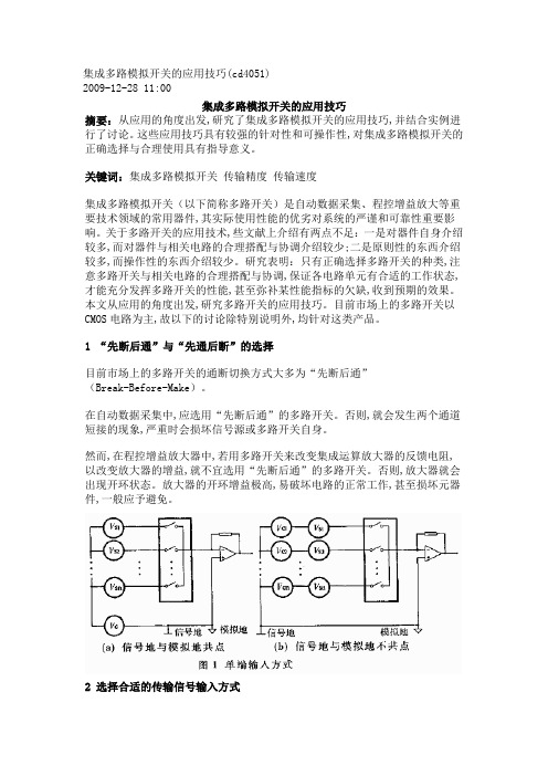
2 选择合适的传输信号输入方式传输信号一般有单端输入和差动输入两种方式,分别适用于不同的场合。
单端输入方式如图1所示,即把所有信号源一端接同一信号地,信号地与ADC等的模拟地相接,各信号源的另一端分别接多路开关。
图中Vs为传输信号,Vc为系统中的共模干扰信号。
CD4514BM96E4中文资料

Data sheet acquired from Harris Semiconductor SCHS074A – Revised June 2003The CD4514B and CD4515B types are supplied in 16-lead hermetic dual-in-line ceramic packages (F3A suffix), 16-lead dual-in-line plastic packages (E suffix), and 16-lead small-outline packages (M and M96 suffixes).PACKAGING INFORMATIONOrderable Device Status(1)PackageType PackageDrawingPins PackageQtyEco Plan(2)Lead/Ball Finish MSL Peak Temp(3)7703201JA ACTIVE CDIP J241TBD Call TI N/A for Pkg Type CD4514BE ACTIVE PDIP N2415Pb-Free(RoHS)CU NIPDAU N/A for Pkg TypeCD4514BEE4ACTIVE PDIP N2415Pb-Free(RoHS)CU NIPDAU N/A for Pkg Type CD4514BF ACTIVE CDIP J241TBD Call TI N/A for Pkg Type CD4514BF3A ACTIVE CDIP J241TBD Call TI N/A for Pkg Type CD4514BM ACTIVE SOIC DW2425Green(RoHS&no Sb/Br)CU NIPDAU Level-1-260C-UNLIMCD4514BM96ACTIVE SOIC DW242000Green(RoHS&no Sb/Br)CU NIPDAU Level-1-260C-UNLIMCD4514BM96E4ACTIVE SOIC DW242000Green(RoHS&no Sb/Br)CU NIPDAU Level-1-260C-UNLIMCD4514BM96G4ACTIVE SOIC DW242000Green(RoHS&no Sb/Br)CU NIPDAU Level-1-260C-UNLIMCD4514BME4ACTIVE SOIC DW2425Green(RoHS&no Sb/Br)CU NIPDAU Level-1-260C-UNLIMCD4514BMG4ACTIVE SOIC DW2425Green(RoHS&no Sb/Br)CU NIPDAU Level-1-260C-UNLIM CD4514BNSR OBSOLETE SO NS24TBD Call TI Call TICD4514BPWR OBSOLETE TSSOP PW24TBD Call TI Call TICD4515BE ACTIVE PDIP N2415Pb-Free(RoHS)CU NIPDAU N/A for Pkg TypeCD4515BEE4ACTIVE PDIP N2415Pb-Free(RoHS)CU NIPDAU N/A for Pkg Type CD4515BF3A ACTIVE CDIP J241TBD Call TI N/A for Pkg Type CD4515BM ACTIVE SOIC DW2425Green(RoHS&no Sb/Br)CU NIPDAU Level-1-260C-UNLIMCD4515BM96ACTIVE SOIC DW242000Green(RoHS&no Sb/Br)CU NIPDAU Level-1-260C-UNLIMCD4515BM96E4ACTIVE SOIC DW242000Green(RoHS&no Sb/Br)CU NIPDAU Level-1-260C-UNLIMCD4515BM96G4ACTIVE SOIC DW242000Green(RoHS&no Sb/Br)CU NIPDAU Level-1-260C-UNLIMCD4515BME4ACTIVE SOIC DW2425Green(RoHS&no Sb/Br)CU NIPDAU Level-1-260C-UNLIMCD4515BMG4ACTIVE SOIC DW2425Green(RoHS&no Sb/Br)CU NIPDAU Level-1-260C-UNLIM(1)The marketing status values are defined as follows:ACTIVE:Product device recommended for new designs.LIFEBUY:TI has announced that the device will be discontinued,and a lifetime-buy period is in effect.NRND:Not recommended for new designs.Device is in production to support existing customers,but TI does not recommend using this part in a new design.PREVIEW:Device has been announced but is not in production.Samples may or may not be available.OBSOLETE:TI has discontinued the production of the device.(2)Eco Plan-The planned eco-friendly classification:Pb-Free(RoHS),Pb-Free(RoHS Exempt),or Green(RoHS&no Sb/Br)-please check /productcontent for the latest availability information and additional product content details.TBD:The Pb-Free/Green conversion plan has not been defined.Pb-Free(RoHS):TI's terms"Lead-Free"or"Pb-Free"mean semiconductor products that are compatible with the current RoHS requirements for all6substances,including the requirement that lead not exceed0.1%by weight in homogeneous materials.Where designed to be soldered at high temperatures,TI Pb-Free products are suitable for use in specified lead-free processes.Pb-Free(RoHS Exempt):This component has a RoHS exemption for either1)lead-based flip-chip solder bumps used between the die and package,or2)lead-based die adhesive used between the die and leadframe.The component is otherwise considered Pb-Free(RoHS compatible)as defined above.Green(RoHS&no Sb/Br):TI defines"Green"to mean Pb-Free(RoHS compatible),and free of Bromine(Br)and Antimony(Sb)based flame retardants(Br or Sb do not exceed0.1%by weight in homogeneous material)(3)MSL,Peak Temp.--The Moisture Sensitivity Level rating according to the JEDEC industry standard classifications,and peak solder temperature.Important Information and Disclaimer:The information provided on this page represents TI's knowledge and belief as of the date that it is provided.TI bases its knowledge and belief on information provided by third parties,and makes no representation or warranty as to the accuracy of such information.Efforts are underway to better integrate information from third parties.TI has taken and continues to take reasonable steps to provide representative and accurate information but may not have conducted destructive testing or chemical analysis on incoming materials and chemicals.TI and TI suppliers consider certain information to be proprietary,and thus CAS numbers and other limited information may not be available for release.In no event shall TI's liability arising out of such information exceed the total purchase price of the TI part(s)at issue in this document sold by TI to Customer on an annual basis.TAPE AND REEL INFORMATION*All dimensions are nominalDevicePackage Type Package Drawing Pins SPQReel Diameter (mm)Reel Width W1(mm)A0(mm)B0(mm)K0(mm)P1(mm)W (mm)Pin1Quadrant CD4514BM96SOIC DW 242000330.024.410.7515.7 2.712.024.0Q1CD4515BM96SOICDW242000330.024.410.7515.72.712.024.0Q1*All dimensions are nominalDevice Package Type Package Drawing Pins SPQ Length(mm)Width(mm)Height(mm) CD4514BM96SOIC DW242000346.0346.041.0 CD4515BM96SOIC DW242000346.0346.041.0IMPORTANT NOTICETexas Instruments Incorporated and its subsidiaries(TI)reserve the right to make corrections,modifications,enhancements,improvements, and other changes to its products and services at any time and to discontinue any product or service without notice.Customers should obtain the latest relevant information before placing orders and should verify that such information is current and complete.All products are sold subject to TI’s terms and conditions of sale supplied at the time of order acknowledgment.TI warrants performance of its hardware products to the specifications applicable at the time of sale in accordance with TI’s standard warranty.Testing and other quality control techniques are used to the extent TI deems necessary to support this warranty.Except where mandated by government requirements,testing of all parameters of each product is not necessarily performed.TI assumes no liability for applications assistance or customer product design.Customers are responsible for their products and applications using TI components.To minimize the risks associated with customer products and applications,customers should provide adequate design and operating safeguards.TI does not warrant or represent that any license,either express or implied,is granted under any TI patent right,copyright,mask work right, or other TI intellectual property right relating to any combination,machine,or process in which TI products or services are rmation published by TI regarding third-party products or services does not constitute a license from TI to use such products or services or a warranty or endorsement e of such information may require a license from a third party under the patents or other intellectual property of the third party,or a license from TI under the patents or other intellectual property of TI.Reproduction of TI information in TI data books or data sheets is permissible only if reproduction is without alteration and is accompanied by all associated warranties,conditions,limitations,and notices.Reproduction of this information with alteration is an unfair and deceptive business practice.TI is not responsible or liable for such altered rmation of third parties may be subject to additional restrictions.Resale of TI products or services with statements different from or beyond the parameters stated by TI for that product or service voids all express and any implied warranties for the associated TI product or service and is an unfair and deceptive business practice.TI is not responsible or liable for any such statements.TI products are not authorized for use in safety-critical applications(such as life support)where a failure of the TI product would reasonably be expected to cause severe personal injury or death,unless officers of the parties have executed an agreement specifically governing such use.Buyers represent that they have all necessary expertise in the safety and regulatory ramifications of their applications,and acknowledge and agree that they are solely responsible for all legal,regulatory and safety-related requirements concerning their products and any use of TI products in such safety-critical applications,notwithstanding any applications-related information or support that may be provided by TI.Further,Buyers must fully indemnify TI and its representatives against any damages arising out of the use of TI products in such safety-critical applications.TI products are neither designed nor intended for use in military/aerospace applications or environments unless the TI products are specifically designated by TI as military-grade or"enhanced plastic."Only products designated by TI as military-grade meet military specifications.Buyers acknowledge and agree that any such use of TI products which TI has not designated as military-grade is solely at the Buyer's risk,and that they are solely responsible for compliance with all legal and regulatory requirements in connection with such use. TI products are neither designed nor intended for use in automotive applications or environments unless the specific TI products are designated by TI as compliant with ISO/TS16949requirements.Buyers acknowledge and agree that,if they use any non-designated products in automotive applications,TI will not be responsible for any failure to meet such requirements.Following are URLs where you can obtain information on other Texas Instruments products and application solutions:Products ApplicationsAmplifiers AudioData Converters AutomotiveDSP BroadbandClocks and Timers Digital ControlInterface MedicalLogic MilitaryPower Mgmt Optical NetworkingMicrocontrollers SecurityRFID TelephonyRF/IF and ZigBee®Solutions Video&ImagingWirelessMailing Address:Texas Instruments,Post Office Box655303,Dallas,Texas75265Copyright©2008,Texas Instruments Incorporated。
MB81V4405C-60资料

NOTE:Permanent device damage may occur if the above Absolute Maximum Ratings are exceeded. Functionaloperation should be restricted to the conditions as detailed in the operational sections of this data sheet.Exposure to absolute maximum rating conditions for extended periods may affect device reliability.MB81V4405C-60/MB81V4405C-70s PRODUCT LINE & FEATURESs PACKAGEParameter MB81V4405C-60MB81V4405C-70 RAS Access Time60 ns max.70 ns max.CAS Access Time15 ns max.20 ns max. Address Access Time30 ns max.35 ns max. Random Cycle Time104 ns min.119 ns min. Hyper Page Mode Cycle Time25 ns min.30 ns min.Low PowerDissipationOperatingcurrentNomal Mode220 mW max.195 mW max.Hyper Page Mode238 mW max.198 mW max.Standby current7.2 mW max. (LVTTL level)/3.6 mW max. (CMOS level)•1,048,576 words × 4 bit organization•Silicon gate, CMOS, Advanced-StackedCapacitor Cell•All input and output are LVTTL compatible•1024 refresh cycles every 16.4 ms•Self refresh function•Early write or OE controlled write capability•RAS-only, CAS-before-RAS, or Hidden Refresh•Hyper page mode, Read-Modify-Write capability•On chip substrate bias generator for highperformancePackage and Ordering Information– 26-pin plastic (300 mil) TSOP-II with normal bend leads, order as MB81V4405C-xxPFTNMB81V4405C-60/MB81V4405C-70s CAPACITANCE(T A = 25°C, f = 1 MHz) Parameter Symbol Typ.Max.UnitInput Capacitance, A0 to A9C IN1—5pFInput Capacitance, RAS, CAS, WE, OE C IN2—7pFInput/Output Capacitance, DQ1 to DQ4C DQ—7pFMB81V4405C-60/MB81V4405C-70 s PIN ASSIGNMENTS AND DESCRIPTIONSMB81V4405C-60/MB81V4405C-70 s RECOMMENDED OPERATING CONDITIONS* :Undershoots of up to –2.0 volts with a pulse width not exceeding 20 ns are acceptable.s FUNCTIONAL OPERATIONADDRESS INPUTSTwenty input bits are required to decode any four of 4,194,304 cell addresses in the memory matrix. Since only ten address bits are available, the column and row inputs are separately strobed by CAS and RAS as shown in Figure 5. First, ten row address bits are input on pins A0-through-A9 and latched with the row address strobe (RAS) then, ten column address bits are input and latched with the column address strobe (CAS). Both row and column ad-dresses must be stable on or before the falling edge of CAS and RAS, respectively. The address latches are of the flow-through type; thus, address information appearing after t RAH (min.) + t T is automatically treated as the column address.WRITE ENABLEThe read or write mode is determined by the logic state of WE. When WE is active Low, a write cycle is initiated; when WE is High, a read cycle is selected. During the read mode, input data is ignored.DATA INPUTInput data is written into memory in either of three basic ways—an early write cycle, an OE (delayed) write cycle, and a read-modify-write cycle. The falling edge of WE or CAS, whichever is later, serves as the input data-latch strobe. In an early write cycle, the input data (DQ1-DQ4) is strobed by CAS and the setup/hold times are referenced to CAS because WE goes Low before CAS. In a delayed write or a read-modify-write cycle, WE goes Low after CAS; thus, input data is strobed by WE and all setup/hold times are referenced to the write-enable signal.DATA OUTPUTThe three-state buffers are LVTTL compatible with a fanout of one TTL loads. Polarity of the output data is identical to that of the input; the output buffers remain in the high-impedance state until the column address strobe goes Low. When a read or read-modify-write cycle is executed, valid outputs and High-Z state are obtained under the following conditions:t RAC:from the falling edge of RAS when t RCD (max.) is satisfied.t CAC:from the falling edge of CAS when t RCD is greater than t RCD (max.).t AA:from column address input when t RAD is greater than t RAD (max.), and t RCD (max.) is satisfied.t OEA:from the falling edge of OE when OE is brought Low after t RAC, t CAC, or t AA.t OEZ:from OE inactive.t OFF:from CAS inactive while RAS inactive.t OFR:from RAS inactive while CAS inactive.t WEZ:from WE active while CAS inactive.The data remains valid after either OE is inactive, or both RAS and CAS are inactive, or CAS is reactived. When an early write is executed, the output buffers remain in a high-impedance state during the entire cycle.Parameter Notes Symbol Min.Typ.Max.Unit AmbientOperating Temp. Supply VoltageV CC 3.0 3.3 3.6V0°C to +70°CV SS000Input High Voltage, all inputs V IH 2.0—V CC +0.3VInput Low Voltage, all inputs*V IL–0.3—0.8V111MB81V4405C-60/MB81V4405C-70HYPER PAGE MODE OF OPERATIONThe hyper page mode operation provides faster memory access and lower power dissipation. The hyper page mode is implemented by keeping the same row address and strobing in successive column addresses. To satisfy these conditions, RAS is held Low for all contiguous memory cycles in which row addresses are common. For each page of memory (within column address locations), any of 1,024 × 4-bits can be accessed and, when multiple MB81V4405Cs are used, CAS is decoded to select the desired memory page. Hyper page mode operations need not be addressed sequentially and combinations of read, write, and/or read-modify-write cycles are permitted. Hyper page mode features that output remains valid when CAS is inactive until CAS is reactivated.MB81V4405C-60/MB81V4405C-70 s DC CHARACTERISTICS(Recommended operating conditions unless otherwise noted.)Notes 3 Parameter Notes Symbol ConditionsValueUnitMin.Typ.Max.Output high voltage V OH I OH = –2 mA 2.4——V Output low voltage V OL I OL = 2 mA——0.4Input leakage current (Any input)I I(L)0 V ≤ V IN≤ 3.6 V;3.0 V ≤ V CC≤ 3.6 V;V SS = 0 V; All other pinsnot under test = 0 V–10—10µA Output leakage current I O(L)0 V ≤ V OUT≤ 3.6 V;Data out disabled–10—10Operating current(Average powersupply current)2MB81V4405C-60I CC1RAS & CAS cycling;t RC = min.——61mA MB81V4405C-7054Standby current(Power supplycurrent)LVTTL levelI CC2RAS = CAS = V IH——2.0mA CMOS level RAS = CAS ≥ V CC –0.2 V 1.0Refresh current #1(Average powersupply current)2MB81V4405C-60I CC3CAS = V IH, RAS cycling;t RC = min.——61mA MB81V4405C-7054Hyper page modecurrent2MB81V4405C-60I CC4RAS = V IL, CAS cycling;t HPC = min.——66mA MB81V4405C-7055Refresh current #2(Average powersupply current)2MB81V4405C-60I CC5RAS cycling;CAS-before-RAS;t RC = min.——49mA MB81V4405C-7044Refresh current #3(Average powersupply current)MB81V4405C-60I CC9RAS = CAS ≤ 0.2 VSelf refresh——1000µA MB81V4405C-70100011MB81V4405C-60/MB81V4405C-70s AC CHARACTERISTICS(At recommended operating conditions unless otherwise noted.)Notes 3, 4, 5(Continued) No.Parameter Notes SymbolMB81V4405C-60MB81V4405C-70UnitMin.Max.Min.Max.1Time Between Refresh t REF—16.4—16.4ms 2Random Read/Write Cycle Time t RC104—119—ns 3Read-Modify-Write Cycle Time t RWC138—156—ns 4Access Time from RAS t RAC—60—70ns 5Access Time from CAS t CAC—15—20ns 6Column Address Access Time t AA—30—35ns 7Output Hold Time t OH5—5—ns 8Output Hold Time from CAS t OHC5—5—ns 9Output Buffer Turn On Delay Time t ON0—0—ns 10Output Buffer T urn Off DelayTimet OFF—15—15ns 11Output Buffer T urn Off Delay Time from RAS t OFR—15—15ns 12Output Buffer Turn Off Delay Time from WE t WEZ—15—15ns 13Transition Time t T150150ns 14RAS Precharge Time t RP40—45—ns 15RAS Pulse Width t RAS6010000070100000ns 16RAS Hold Time t RSH15—20—ns 17CAS to RAS Precharge Time t CRP0—0—ns 18RAS to CAS Delay Time t RCD14451450ns 19CAS Pulse Width t CAS10100001010000ns 20CAS Hold Time t CSH40—50—ns 21CAS Precharge Time (Normal)t CPN10—10—ns 22Row Address Set Up Time t ASR0—0—ns 23Row Address Hold Time t RAH10—10—ns 24Column Address Set Up Time t ASC0—0—ns 25Column Address Hold Time t CAH10—10—ns 26RAS to Column Address DelayTimet RAD12301235ns 27Column Address to RAS Lead Time t RAL30—35—ns 28Column Address to CAS Lead Time t CAL23—28—ns 29Read Command Set Up Time t RCS0—0—ns 30Read Command Hold TimeReferenced to RASt RRH0—0—ns6, 97, 98, 9102111, 12, 22191314MB81V4405C-60/MB81V4405C-70 s AC CHARACTERISTICS (Continued)(At recommended operating conditions unless otherwise noted.)Notes 3, 4, 5(Continued) No.Parameter Notes SymbolMB81V4405C-60MB81V4405C-70UnitMin.Max.Min.Max.31Read Command Hold TimeReferenced to CASt RCH0—0—ns 32Write Command Set Up Time t WCS0—0—ns 33Write Command Hold Time t WCH10—10—ns 34WE Pulse Width t WP10—10—ns 35Write Command to RAS Lead Time t RWL15—18—ns 36Write Command to CAS Lead Time t CWL10—10—ns 37DIN Set Up Time t DS0—0—ns 38DIN Hold Time t DH10—10—ns 39RAS to WE Delay Time t RWD77—87—ns 40CAS to WE Delay Time t CWD32—37—ns 41Column Address to WE Delay Time t AWD47—52—ns 42RAS Precharge Time to CAS Active Time(Refresh Cycles)t RPC5—5—ns 43CAS Set Up Time for CAS-before-RASRefresht CSR0—0—ns 44CAS Hold Time for CAS-before-RASRefresht CHR10—10—ns 45WE Set Up Time from RAS t WSR0—0—ns 46WE Hold Time from RAS t WHR10—10—ns 47Access Time from OE t OEA—15—20ns 48Output Buffer T urn Off Delayfrom OEt OEZ—15—15ns 49OE to RAS Lead Time for Valid Data t OEL10—10—ns 50OE to CAS Lead Time t COL5—5—ns 51OE Hold Time Referenced toWEt OEH0—0—ns 52OE to Data In Delay Time t OED15—15—ns 53DIN to CAS Delay Time t DZC0—0—ns 54DIN to OE Delay Time t DZO0—0—ns 55OE Precharge Time t OEP10—10—ns 56OE Hold Time Referenced to CAS t OECH10—10—ns 57WE Precharge Time t WPZ10—10—ns 58WE to Data In Delay Time t WED15—15—ns 59RAS to Data In Delay Time t RDD15—15—ns 60CAS to Data In Delay Time t CDD15—15—ns14152020910161717MB81V4405C-60/MB81V4405C-70s AC CHARACTERISTICS (Continued)(At recommended operating conditions unless otherwise noted.)Notes 3, 4, 5No.Parameter Notes SymbolMB81V4405C-60MB81V4405C-70UnitMin.Max.Min.Max.61RAS to Columunn Address Hold Time t AR26—26—ns 62Write Command Hold Time Referenced toRASt WCR24—24—ns 63Data Input Hold Time Referenced to RAS t DHR24—24—ns 64Hyper Page Mode Read/Write Cycle Time t HPC25—30—ns 65Hyper Page Mode Read-Modify-Write CycleTimet HPRWC66—71—ns 66Access Time from CASPrecharget CPA—35—40ns 67Hyper Page Mode CAS Precharge Time t CP10—10—ns 68Hyper Page Mode RAS Pulse Width t RASP—200000—200000ns 69Hyper Page Mode RAS Hold Time fromCAS Precharget RHCP35—40—ns 70Hyper Page Mode CAS Precharge to WEDelay Timet CPWD52—57—ns9, 18Notes:1.Referenced to V SS.2.I CC depends on the output load conditions and cycle rates; The specified values are obtained with theoutput open.I CC depends on the number of address change as RAS = V IL and CAS = V IH.I CC1, I CC3 and I CC5 are specified at one time of address change during RAS = V IL and CAS = V IH.I CC4 is specified at one time of address change during one Page cycle.3.An Initial pause (RAS = CAS = V IH) of 200 µs is required after power-up followed by any eight RAS-only cycles before proper device operation is achieved. In case of using internal refresh counter, aminimum of eight CAS-before-RAS initialization cycles instead of 8 RAS cycles are required.4.AC characteristics assume t T = 2 ns.5.V IH (min.) and V IL (max.) are reference levels for measuring timing of input signals. Also transition timesare measured between V IH (min.) and V IL (max.).6.Assumes that t RCD ≤ t RCD (max.), t RAD≤ t RAD (max.). If t RCD is greater than the maximum recommendedvalue shown in this table, t RAC will be increased by the amount that t RCD exceeds the value shown. Referto Fig. 2 and 3.7.If t RCD ≥ t RCD (max.), t RAD≥ t RAD (max.), and t ASC ≥ t AA – t CAC – t T, access time is t CAC.8.If t RAD ≥ t RAD (max.) and t ASC ≤ t AA – t CAC – t T, access time is t AA.9.Measured with a load equivalent to one TTL loads and 100 pF.10.t OFF and t OEZ is specified that output buffer change to high impedance state.11.Operation within the t RCD (max.) limit ensures that t RAC (max.) can be met. t RCD (max.) is specified as areference point only; if t RCD is greater than the specified t RCD (max.) limit, access time is controlledexclusively by t CAC or t AA.12.t RCD (min.) = t RAH (min.) + 2t T + t ASC (min.).13.Operation within the t RAD (max.) limit ensures that t RAC (max.) can be met. t RAD (max.) is specified as areference point only; if t RAD is greater than the specified t RAD (max.) limit, access time is controlledexclusively by t CAC or t AA.14.Either t RRH or t RCH must be satisfied for a read cycle.15.t WCS is specified as a reference point only. If t WCS ≥ t WCS (min.) the data output pin will remain High-Zstate through entire cycle.16.Assumes that t WCS < t WCS (min.).17.Either t DZC or t DZO must be satisfied.18.t CP A is access time from the selection of a new column address (that is caused by changing CAS from“L” to “H”). Therefore, if t CP is long, t CP A is longer than t CP A (max.) as shown in Fig. 4.19.Assumes that CAS-before-RAS refresh.20.Assumes that T est mode function.21.The last CAS rising edge.22.The first CAS falling edge.s FUNCTIONAL TRUTH TABLEX; “H” or “L ”*; It is impossible in Hyper Page Mode.Operation Mode Clock Input Address Input Data Refresh NoteRAS CAS WE OE Row Column Input OutputStandby H H X X ———High-Z —Read Cycle L L H L Valid Valid —Valid Yes*t RCS ≥ t RCS (min.)Write Cycle (Early Write)L L LXValid Valid Valid High-Z Yes*t WCS ≥ t WCS (min.)Read-Modify-Write Cycle L L H →L L →H Valid Valid Valid Valid Yes*t CWD ≥ t CWD (min.)RAS-only Refresh Cycle L H X X Valid ——High-Z Yes CAS-before-RAS Refresh Cycle L L H X ———High-Z Yes t CSR ≥ t CSR (min.)Hidden Refresh Cycle H →L L H L ———Valid Yes Previous data is keptTest mode Set Cycle (CBR)L L L X ———High-Z Yes t CSR ≥ t CSR (min.)t WSR ≥ t WSR (min.)Test mode Set Cycle (Hidden)H →LLLX———ValidYest CSR ≥ t CSR (min.)t WSR ≥ t WSR (min.)MB81V4405C-60/MB81V4405C-70MB81V4405C-60/MB81V4405C-70MB81V4405C-60/MB81V4405C-70MB81V4405C-60/MB81V4405C-70MB81V4405C-60/MB81V4405C-70MB81V4405C-60/MB81V4405C-70MB81V4405C-60/MB81V4405C-70MB81V4405C-60/MB81V4405C-70MB81V4405C-60/MB81V4405C-70 s PACKAGE DIMENSIONSAll Rights Reserved.The contents of this document are subject to change without notice. Customers are advised to consult with FUJITSU sales representatives before ordering.The information and circuit diagrams in this document presented as examples of semiconductor device applications, and are not intended to be incorporated in devices for actual use. Also, FUJITSU is unable to assume responsibility for infringement of any patent rights or other rights of third parties arising from the use of this information or circuit diagrams.FUJITSU semiconductor devices are intended for use in standard applications (computers, office automation and other office equipment, industrial, communications, and measurement equipment, personal or household devices, etc.). CAUTION:Customers considering the use of our products in special applications where failure or abnormal operation may directly affect human lives or cause physical injury or property damage, or where extremely high levels of reliability are demanded (such as aerospace systems, atomic energy controls, sea floor repeaters, vehicle operating controls, medical devices for life support, etc.) are requested to consult with FUJITSU sales representatives before such use. The company will not be responsible for damages arising from such use without prior approval.Any semiconductor devices have inherently a certain rate of failure. You must protect against injury, damage or loss from such failures by incorporating safety design measures into your facility and equipment such as redundancy, fire protection, and prevention of over-current levels and other abnormal operating conditions.If any products described in this document represent goods or technologies subject to certain restrictions on export under the Foreign Exchange and Foreign Trade Control Law of Japan, the prior authorization by Japanese government should be required for export of those products from Japan.。
IC集成电路型号大全及40系列芯片功能大全

IC集成电路型号大全及40系列芯片功能大全CD4001 四2输入端或者非门CD4002 双4输入端或者非门CD4006 18位串入/串出移位寄存器CD4007 双互补对加反相器CD4008 4位超前进位全加器CD4009 六反相缓冲/变换器CD4010 六同相缓冲/变换器CD4011 四2输入端与非门CD4012 双4输入端与非门CD4013 双主-从D型触发器CD4014 8位串入/并入-串出移位寄存器CD4015 双4位串入/并出移位寄存器CD4016 四传输门CD4017 十进制计数/分配器CD4018 可预制1/N计数器CD4019 四与或者选择器CD4020 14级串行二进制计数/分频器CD4021 08位串入/并入-串出移位寄存器CD4022 八进制计数/分配器CD4023 三3输入端与非门CD4024 7级二进制串行计数/分频器CD4025 三3输入端或者非门CD4026 十进制计数/7段译码器CD4027 双J-K触发器CD4028 BCD码十进制译码器CD4029 可预置可逆计数器CD4030 四异或者门CD4031 64位串入/串出移位存储器CD4032 三串行加法器CD4033 十进制计数/7段译码器CD4034 8位通用总线寄存器CD4035 4位并入/串入-并出/串出移位寄存CD4038 三串行加法器CD4040 12级二进制串行计数/分频器CD4041 四同相/反相缓冲器CD4042 四锁存D型触发器CD4043 三态R-S锁存触发器("1"触发)CD4044 四三态R-S锁存触发器("0"触发)CD4046 锁相环CD4047 无稳态/单稳态多谐振荡器CD4048 四输入端可扩展多功能门CD4049 六反相缓冲/变换器CD4050 六同相缓冲/变换器CD4051 八选一模拟开关CD4052 双4选1模拟开关CD4053 三组二路模拟开关CD4054 液晶显示驱动器CD4055 BCD-7段译码/液晶驱动器CD4056 液晶显示驱动器CD4059 “N”分频计数器 NSC/TICD4060 14级二进制串行计数/分频器CD4063 四位数字比较器CD4066 四传输门CD4067 16选1模拟开关CD4068 八输入端与非门/与门CD4069 六反相器CD4070 四异或者门CD4071 四2输入端或者门CD4072 双4输入端或者门CD4073 三3输入端与门CD4075 三3输入端或者门CD4076 四D寄存器CD4077 四2输入端异或者非门CD4078 8输入端或者非门/或者门CD4081 四2输入端与门CD4082 双4输入端与门CD4085 双2路2输入端与或者非门CD4086 四2输入端可扩展与或者非门CD4089 二进制比例乘法器CD4093 四2输入端施密特触发器CD4095 三输入端J-K触发器CD4096 三输入端J-K触发器CD4097 双路八选一模拟开关CD4098 双单稳态触发器CD4099 8位可寻址锁存器CD40100 32位左/右移位寄存器CD40101 9位奇偶较验器CD40102 8位可预置同步BCD减法计数器CD40103 8位可预置同步二进制减法计数器CD40104 4位双向移位寄存器CD40105 先入先出FI-FD寄存器CD40106 六施密特触发器CD40107 双2输入端与非缓冲/驱动器CD40108 4字×4位多通道寄存器CD40109 四低-高电平位移器CD40110 十进制加/减,计数,锁存,译码驱动CD40147 10-4线编码器CD40160 可预置BCD加计数器CD40161 可预置4位二进制加计数器CD40162 BCD加法计数器CD40163 4位二进制同步计数器CD40174 六锁存D型触发器CD40175 四D型触发器CD40181 4位算术逻辑单元/函数发生器CD40182 超前位发生器CD40192 可预置BCD加/减计数器(双时钟) CD40193 可预置4位二进制加/减计数器CD40194 4位并入/串入-并出/串出移位寄存CD40195 4位并入/串入-并出/串出移位寄存CD40208 4×4多端口寄存器CD4501 4输入端双与门及2输入端或者非门CD4502 可选通三态输出六反相/缓冲器CD4503 六同相三态缓冲器CD4504 六电压转换器CD4506 双二组2输入可扩展或者非门CD4508 双4位锁存D型触发器CD4510 可预置BCD码加/减计数器CD4511 BCD锁存,7段译码,驱动器CD4512 八路数据选择器CD4513 BCD锁存,7段译码,驱动器(消隐) CD4514 4位锁存,4线-16线译码器CD4515 4位锁存,4线-16线译码器CD4516 可预置4位二进制加/减计数器CD4517 双64位静态移位寄存器CD4518 双BCD同步加计数器CD4519 四位与或者选择器CD4520 双4位二进制同步加计数器CD4521 24级分频器CD4522 可预置BCD同步1/N计数器CD4526 可预置4位二进制同步1/N计数器CD4527 BCD比例乘法器CD4528 双单稳态触发器CD4529 双四路/单八路模拟开关CD4530 双5输入端优势逻辑门CD4531 12位奇偶校验器CD4532 8位优先编码器CD4536 可编程定时器CD4538 精密双单稳CD4539 双四路数据选择器CD4541 可编程序振荡/计时器CD4543 BCD七段锁存译码,驱动器CD4544 BCD七段锁存译码,驱动器CD4547 BCD七段译码/大电流驱动器CD4549 函数近似寄存器CD4551 四2通道模拟开关CD4553 三位BCD计数器CD4555 双二进制四选一译码器/分离器CD4556 双二进制四选一译码器/分离器CD4558 BCD八段译码器CD4560 "N"BCD加法器CD4561 "9"求补器CD4573 四可编程运算放大器CD4574 四可编程电压比较器CD4575 双可编程运放/比较器CD4583 双施密特触发器CD4584 六施密特触发器CD4585 4位数值比较器CD4599 8位可寻址锁存器CD22100 4×4×1交叉点开关0206A 天线开关集成电路03VFG9 发射压控振荡集成电路1021AC 发射压控振荡集成电路1097C 升压集成电路140N 电源取样比较放大集成电路14DN363 伺服操纵集成电路15105 充电操纵集成电路15551 管理卡升压集成电路1710 视频信号处理集成电路1N706 混响延时集成电路20810-F6096 存储集成电路2252B 微处理集成电路2274 延迟集成电路24C01ACEA 存储集成电路24C026 存储集成电路24C04 存储集成电路24C64 码片集成电路24LC16B 存储集成电路24LC65 电可改写编程只读存储集成电路27C1000PC-12 存储集成电路27C2000QC-90 存储集成电路27C20T 存储集成电路27C512 电可改写编程只读存储集成电路2800 红外遥控信号接收集成电路28BV64 码片集成电路28F004 版本集成电路31085 射频电源集成电路32D54 电源、音频信号处理集成电路1732D75 电源、音频信号处理集成电路32D92 电源中频放大集成电路4066B 电子开关切换集成电路4094 移位寄存串入、并出集成电路424260SDJ 存储集成电路4260 动态随机存储集成电路4270351/91B9905 中频放大集成电路4370341/90M9919 中频处理集成电路4464 存储集成电路4558 双运算放大集成电路4580D 双运算放大集成电路47C1638AN-U337 微处理集成电路47C1638AU-353 微处理集成电路47C432GP 微处理集成电路47C433AN-3888 微处理集成电路49/4CR1A 中频放大集成电路5101 天线开关集成电路5G052 发光二极管四位显示驱动集成电路5G24 运算放大集成电路5W01 双运算放大集成电路649/CRIA70612 中频放大集成电路673/3CR2A 多模转换集成电路74122 可重触发单稳态集成电路74HC04 逻辑与非门集成电路74HC04D 六反相集成电路74HC123 单稳态集成电路74HC125 端口功能扩展集成电路74HC14N 六反相集成电路74HC157A 多路转换集成电路74HC165 移相寄存集成电路1874HC245 总线收发集成电路74HC32 或者门四2输入集成电路74HC374八D 触发集成电路74HC573D 存储集成电路74HCT157 多路转换双输入集成电路74HCT4046A 压控振荡集成电路74HCT4538D 单稳态集成电路74HCT4538N 触发脉冲集成电路74HCT86D 异或者门四2输入集成电路74HCU04 与非门集成电路74LS125 端口功能扩展集成电路74LS373 锁存集成电路74LS393 计数双四位二进制集成电路74LS74双D 触发集成电路78014DFP 系统操纵处理集成电路811N 伴音阻容偏置集成电路83D33 压控振荡集成电路85712 场扫描信号校正处理集成电路85713 行扫描信号校正集成电路87C52 微处理集成电路87CK38N-3584 微处理集成电路87CK38N-3627 微处理集成电路89C52 系统操纵处理集成电路89C55 系统操纵处理集成电路93C66 电可改写编程只读存储集成电路93LC56 电可改写编程存储集成电路9821K03 系统操纵集成电路A1642P 背景歌声消除集成电路A701 红外遥控信号接收集成电路A7950 场频识别集成电路19A8772AN 色差信号延迟处理集成电路A9109 功率放大集成电路AAB 电源集成电路ACA650 色度信号解调集成电路ACFP2 色度、亮度信号分离集成电路ACP2371 多伴音、多语言改善集成电路ACVP2205 色度、亮度信号分离集成电路AD1853 立体声数/模转换集成电路AD1858 音频解调集成电路AD722 视频编码集成电路ADC2300E 音频数/模转换集成电路ADC2300J 音频数/模转换集成电路ADC2310E 音频数/模转换集成电路ADV7172 视频编码集成电路ADV7175A 视频编码集成电路AE31201 频率显示集成电路AJ7080 射频调制集成电路AK4321-VF-E1 音频数/模转换集成电路AN1319 双高速电压比较集成电路AN1358S 双运算放大集成电路AN1393 双运算放大集成电路AN1431T 稳压电源集成电路AN1452 音频前置放大集成电路AN1458S 双运算放大集成电路AN206 伴音中频及前置放大集成电路AN222 自动频率操纵集成电路AN236 副载波信号处理集成电路AN239Q 图像、伴音中频放大集成电路AN247P 图像中频放大、AGC操纵集成电路AN253P 调频/调幅中频放大集成电路20AN262 音频前置放大集成电路AN2661NK 视频信号处理集成电路AN2663K 视频信号处理集成电路AN272 音频功率放大集成电路AN2751FAP 视频信号处理集成电路AN281 色度解码集成电路AN2870FC 多功能操纵集成电路AN295 行、场扫描信号处理集成电路AN301 伺服操纵集成电路AN305 视频自动增益操纵集成电路AN306 色度自动相位操纵集成电路AN318 直流伺服操纵集成电路AN320 频率操纵、调谐显示驱动集成电路AN3215K 视频信号处理集成电路AN3215S 视频信号处理集成电路AN3224K 磁头信号记录放大集成电路AN3248NK 亮度信号记录、重放处理集成电路AN331 视频信号处理集成电路AN3311K 磁头信号放大集成电路AN3313 磁头信号放大集成电路AN3321S 录像重放信号处理集成电路AN3331K 磁头信号处理集成电路AN3337NSB 磁头信号放大集成电路AN3380K 磁头信号处理集成电路AN3386NK 磁头信号处理集成电路AN3495K 色度、亮度信号降噪集成电路AN355 伴音中频放大、检波集成电路AN3581S 视频驱动集成电路AN366 调频/调幅中频放大集成电路AN3791 移位操纵集成电路21AN3792 磁鼓伺服操纵接口集成电路AN3795 主轴伺服操纵接口集成电路AN3814K 电机驱动集成电路AN4265 音频功率放大集成电路AN4558 运算放大集成电路AN5010 电子选台集成电路AN5011 电子选台集成电路AN5015K 电子选台集成电路AN5020 红外遥控信号接收集成电路AN5025S 红外遥控信号接收集成电路AN5026K 红外遥控信号接收集成电路AN5031 电调谐操纵集成电路AN5034 调谐操纵集成电路AN5036 调谐操纵集成电路AN5043 调谐操纵集成电路AN5071 频段转换集成电路AN5095K 电视信号处理集成电路AN5110 图像中频放大集成电路AN5130 图像中频、视频检波放大集成电路AN5138NK 图像、伴音中频放大集成电路AN5156K 电视信号处理集成电路AN5177NK 图像、伴音中频放大集成电路AN5179K 图像、伴音中频放大集成电路AN5183K 中频信号处理集成电路AN5195K 中频、色度、扫描信号处理集成电路AN5215 伴音信号处理集成电路AN5520 伴音中频放大及鉴频集成电路AN5222 伴音中频放大集成电路AN5250 伴音中频放大、鉴频及功率放大集成电路AN5262 音频前置放大集成电路22AN5265 音频功率放大集成电路AN5270 音频功率放大集成电路AN5273 双声道音频功率放大集成电路AN5274 双声道音频功率放大集成电路AN5275 中置、3D放大集成电路AN5285K 双声道前置放大集成电路AN5295NK 音频信号切换集成电路AN5312 视频、色度信号处理集成电路AN5313NK 视频、色度信号处理集成电路AN5342 图像水平轮廓校正集成电路AN5342FB 水平清晰度操纵集成电路AN5344FBP 色度信号处理集成电路AN5348K 人工智能信号处理集成电路AN5385K 色差信号放大集成电路AN5410 行、场扫描信号处理集成电路AN5421 同步检测集成电路AN5422 行、场扫描信号处理集成电路AN5512 场扫描输出集成电路AN5515 场扫描输出集成电路AN5521 场扫描输出集成电路AN5532 场扫描输出集成电路AN5534 场扫描输出集成电路AN5551 枕形校正集成电路AN5560 场频识别集成电路AN5600K 中频、亮度、色度及扫描信号处理集成电路AN5601K 视频、色度、同步信号处理集成电路AN5607K 视频、色度、行场扫描信号处理集成电路AN5615 视频信号处理集成电路AN5620X 色度信号处理集成电路AN5621 场扫描输出集成电路23AN5625 色度信号处理集成电路AN5633K 色度信号处理集成电路AN5635 色度解码集成电路AN5635NS 色度解码集成电路AN5637 色度解码、亮度延迟集成电路AN5650 同步信号分离集成电路AN5682K 基色电子开关切换集成电路AN5693K 视频、色度、行场扫描信号处理集成电路AN5712 图像中频放大、AGC操纵集成电路AN5722 图像中频放大、检波集成电路AN5732 伴音中频放大、鉴频集成电路AN5743 音频功率放大集成电路AN5750 行自动频率操纵及振荡集成电路AN5757S 行扫描电源电压操纵集成电路AN5762 场扫描振荡、输出集成电路AN5764 光栅水平位置操纵集成电路AN5765 电源稳压操纵集成电路AN5767 同步信号处理集成电路AN5768 光栅倾斜校正操纵集成电路AN5769 行、场会聚操纵集成电路AN5790N 行扫描信号处理集成电路AN5791 同步脉冲相位与脉宽调整集成电路AN5803 双声道立体声解调集成电路AN5836 双声道前置放大集成电路AN5858K 视频信号操纵集成电路AN5862 视频信号操纵集成电路AN5862S-E1 视频信号开关操纵集成电路AN5870K 模拟信号切换集成电路AN5891K 音频信号处理集成电路AN614 行枕形校正集成电路24AN6210 双声道前置放大集成电路AN6306S 亮度信号处理集成电路AN6308 模拟电子开关集成电路AN6327 视频重放信号处理集成电路AN6341N 伺服操纵集成电路AN6342N 基准分频集成电路AN6344 伺服操纵集成电路AN6345 分频集成电路AN6346N 磁鼓伺服操纵集成电路AN6350 磁鼓伺服操纵集成电路AN6357N 主轴接口集成电路AN6361N 色度信号处理集成电路AN6367NK 色度信号处理集成电路AN6371S 自动相位操纵集成电路AN6387 电机伺服操纵集成电路AN6550 卡拉OK音频放大集成电路AN6554 四运算放大集成电路AN6561 双运算放大集成电路AN6562SG 双运算放大集成电路AN6609N 电机驱动集成电路AN6612 电机稳速操纵集成电路AN6650 电机速度操纵集成电路AN6651 电机速度操纵集成电路AN6652 电机稳速操纵集成电路AN6875 发光二极管五位显示驱动集成电路AN6877 发光二极管七位显示驱动集成电路AN6884 发光二极管五位显示驱动集成电路AN6886 发光二极管五位显示驱动集成电路AN6888 发光二极管显示驱动集成电路AN6914 双电压比较集成电路25AN7085N5 单片录、放音集成电路AN7105 双声道音频功率放大集成电路AN7106K 双声道音频功率放大集成电路AN7108 单片立体声放音集成电路AN710S 单片放音集成电路AN7110E 音频功率放大集成电路AN7114 音频功率放大集成电路AN7116 音频功率放大集成电路AN7118 双声道音频功率放大集成电路AN7118S 双声道音频功率放大集成电路AN7120 音频功率放大集成电路AN7124 双声道音频功率放大集成电路AN7145 双声道音频功率放大集成电路AN7148 双声道音频功率放大集成电路AN7158N 音频功率放大7.5W×2集成电路AN7161N 音频功率放大集成电路AN7164 双声道音频功率放大集成电路AN7171NK 音频功率放大集成电路AN7205 调频/调谐及高频放大集成电路AN7220 调频/调幅中频放大集成电路AN7222 调频/调幅中频放大集成电路AN7223 调频/调幅中频放大集成电路AN7226 调频/调幅中频放大集成电路AN7256 调频/调谐及中频放大集成电路AN7311 双声道前置放大集成电路AN7312 双声道前置放大集成电路AN7315 双声道前置放大集成电路AN7315S 双声道前置放大集成电路AN7320 音频前置放大集成电路AN7396K 双声道前置放大集成电路26AN7397K 双声道前置放大集成电路AN7410 调频立体声多路解码集成电路AN7414 调频立体声解码集成电路AN7420N 调频立体声解码集成电路AN7470 调频立体声解码集成电路AN7805 三端电源稳压+5V/1A集成电路AN7806 三端电源稳压+6V/1A集成电路AN7807 三端电源稳压+7V/1A集成电路AN7808 三端电源稳压+8V/1A集成电路AN7809 电源稳压+9V/1A集成电路AN7810 三端电源稳压+10V/1A集成电路AN7812 三端电源稳压+12V/1A集成电路AN7815 三端电源稳压+15V/1A集成电路AN7818 三端电源稳压+18V/1A集成电路AN7820 三端电源稳压+20V/1A集成电路AN7824 三端电源稳压+24V/1A集成电路AN78L05 三端电源稳压+5V/0.1A集成电路AN78L06 三端电源稳压+6V/0.1A集成电路AN78L08 三端电源稳压+8V/0.1A集成电路AN78L09 三端电源稳压+9V/0.1A集成电路AN78L10 三端电源稳压+10V/0.1A集成电路AN78L12 三端电源稳压+12V/0.1A集成电路AN78L15 三端电源稳压+15V/0.1A集成电路AN78L18 三端电源稳压+18V/0.1A集成电路AN78L20 三端电源稳压+20V/0.1A集成电路AN78L24 三端电源稳压+24V/0.1A集成电路AN78M05 三端电源稳压+5V/0.5A集成电路AN78M06 三端电源稳压+6V/0.5A集成电路AN78M08 三端电源稳压+8V/0.5A集成电路AN78M09 三端电源稳压+9V/0.5A集成电路27AN78M10 三端电源稳压+10V/0.5A集成电路AN78M12 三端电源稳压+12V/0.5A集成电路AN78M15 三端固定式稳压+15V/0.5A集成电路AN78M18 三端电源稳压+18V/0.5A集成电路AN78M20 三端电源稳压+20V/0.5A集成电路AN78M24 三端电源稳压+24V/0.5A集成电路AN7905 三端电源稳压-5V/1A集成电路AN7906 三端电源稳压-6V/1A集成电路AN7908T 三端电源稳压-8V/1A集成电路AN7909T 三端电源稳压-9V/1A集成电路AN7910T 三端电源稳压-10V/1A集成电路AN7912 三端电源稳压-12V/1A集成电路AN7915 三端电源稳压-15V/1A集成电路AN7918 三端电源稳压-18V/1A集成电路AN7920 三端电源稳压-20V/1A集成电路AN7924 三端电源稳压-24V/1A集成电路AN79L05 三端电源稳压-5V/0.1A集成电路AN79L06 三端电源稳压-6V/0.1A集成电路AN79L08 三端电源稳压-8V/0.1A集成电路AN79L09 三端电源稳压-9V/0.1A集成电路AN79L10 三端电源稳压-10V/0.1A集成电路AN79L12 三端电源稳压-12V/0.1A集成电路AN79L15 三端电源稳压-15V/0.1A集成电路AN79L18 三端电源稳压-18V/0.1A集成电路AN79L20 三端电源稳压-20V/0.1A集成电路AN79L24 三端电源稳压-24V/0.1A集成电路AN79M05 三端电源稳压-5V/0.5A集成电路AN79M06 三端电源稳压-6V/0.5A集成电路AN79M08 三端电源稳压-8V/0.5A集成电路AN79M09 三端电源稳压-9V/0.5A集成电路28AN79M10 三端电源稳压-10V/0.5A集成电路AN79M12 三端电源稳压-12V/0.5A集成电路AN79M15 三端电源稳压-15V/0.5A集成电路AN79M18 三端电源稳压-18V/0.5A集成电路AN79M20 三端电源稳压-20V/0.5A集成电路AN79M24 三端电源稳压-24V/0.5A集成电路AN8028 自激式开关电源操纵集成电路AN8270K 主轴电机操纵集成电路AN8280 电机驱动集成电路AN8281S 电机驱动集成电路AN8290S 主轴电机驱动集成电路AN8355S 条形码扫描接收集成电路AN8370S 光电伺服操纵集成电路AN8373S 射频伺服处理集成电路AN8375S 伺服处理集成电路AN8389S-E1 电机驱动集成电路AN8480NSB 主轴电机驱动集成电路AN8481SB-E1 主轴电机驱动集成电路AN8482SB 主轴电机驱动集成电路AN8623FBQ 主轴伺服处理集成电路AN8788FB 电机驱动集成电路AN8802CE1V 伺服处理集成电路AN8813NSBS 主轴电机驱动集成电路AN8819NFB 伺服驱动、直流交换集成电路AN8824FBQ 前置放大集成电路AN8825NFHQ-V 聚焦、循迹误差处理集成电路AN8831SC 视频预视放集成电路AN8832SB-E1 射频放大、伺服处理集成电路AN8837SB-E1 伺服处理集成电路AN89C2051-24PC 微处理集成电路29APU2400U 音频信号处理集成电路APU2470 音频信号处理集成电路AS4C14405-60JC 动态随机存储1M×4集成电路AS4C256K16ED-60JC 存储集成电路ASD0204-015 图文操纵集成电路ASD0204GF-022-3BA显示操纵集成电路AT24C08 存储集成电路AT24C08A 存储集成电路AT24C256-10CI 码片集成电路AT27C010 电可改写编程只读存储集成电路AT27C020 存储集成电路ATMEL834 存储集成电路AVM-1 视频信号处理厚膜集成电路AVM-2 音频信号处理厚膜集成电路AVSIBCP08 倍压整流切换集成电路B0011A 存储集成电路B1218 电子快门操纵集成电路BA033T 三端电源稳压+3.3V集成电路BA10324 四运算放大集成电路BA10393N 双运算放大集成电路BA1102F 杜比降噪处理集成电路BA1106F 杜比降噪处理集成电路BA12ST 电源稳压集成电路BA1310 调频立体声解码集成电路BA1332L 调频立体声解码集成电路BA1350 调频立体声解码集成电路BA1351 调频立体声解码集成电路BA1356 调频立体声解码集成电路BA1360 调频立体声解码集成电路BA15218N 双运算放大集成电路30BA225 可触发双单稳态振荡集成电路BA302 音频前置放大集成电路BA311 音频前置放大集成电路BA313 音频前置放大集成电路BA3283 单片放音集成电路BA328F 双声道前置放大集成电路BA329 双声道前置放大集成电路BA3304F 录放音前置均衡放大集成电路BA3306 音频、前置放大集成电路BA3312N 话筒信号前置放大集成电路BA3313L 自动音量操纵集成电路BA3314 话筒信号前置放大集成电路BA335 自动选曲集成电路BA336 自动选曲集成电路BA340 音频前置放大集成电路BA3402F 双声道前置放大集成电路BA3404F 自返转放音集成电路BA343 双声道前置放大集成电路BA3503F 双声道前置放大集成电路BA3506 单片放音集成电路BA3513FS 单片放音集成电路BA3516 单片放音集成电路BA3706 自动选曲集成电路BA3707 录音带曲间检测集成电路BA3812L 五频段音调补偿集成电路BA3818F 电压比较运放集成电路BA3822LS 双声道五频段显示均衡集成电路BA3828 电子选台预置集成电路BA3880 音频处理集成电路31BA401 调频中频放大集成电路BA402 调频中频放大集成电路BA4110 调频中频放大集成电路BA4234L 调频中频放大集成电路BA4402 调频调谐收音集成电路BA4403 调频高频放大、混频、本振集成电路BA4560 双运算放大集成电路BA5096 数字混响集成电路BA5102A 音频功率放大集成电路BA514 音频功率放大集成电路BA516 音频功率放大集成电路BA5208AF 音频功率放大集成电路BA532 音频功率放大集成电路BA534 音频功率放大集成电路BA5406 双声道音频功率放大集成电路BA5412 音频功率放大集成电路BA547 音频功率放大1.5W集成电路BA5912AFP-YE2 电机驱动、倾斜、加载集成电路BA5981FP-E2 聚焦、循迹驱动集成电路BA5983FB 四通道伺服驱动集成电路BA5983FM-E2 电机驱动集成电路BA6104 发光二极管五位显示驱动集成电路BA6107A 电机伺服操纵集成电路BA6109 加载电机驱动集成电路BA6125 发光二极管五位显示驱动集成电路BA6137 发光二极管五位显示驱动集成电路BA6191 音频操纵集成电路BA6196FP 伺服驱动集成电路BA6208 电机驱动集成电路BA6208D 电机驱动集成电路32BA6209 电机驱动集成电路BA6209N 双向驱动电机集成电路BA6218 加载电机驱动集成电路BA6219 电机驱动集成电路BA6219B 电机驱动集成电路BA6227 电机稳速操纵集成电路BA6238 电机驱动集成电路BA6239 电机双向驱动集成电路BA6239A 电机双向驱动集成电路BA6246M 加载、转盘电机驱动集成电路BA6248 电机驱动集成电路BA6286 电机驱动集成电路BA6287 电机驱动集成电路BA6290 电机驱动集成电路BA6295AFP-E2 加载、倾斜驱动集成电路BA6296FP 电机速度操纵集成电路BA6297AFP 伺服驱动集成电路BA6302A 电机伺服操纵集成电路BA6305 操纵放大集成电路BA6305F 操纵放大集成电路BA6308 电子开关切换集成电路BA6321 电机伺服操纵集成电路BA6392 伺服驱动集成电路BA6395 主轴电机驱动集成电路BA6396FP 伺服驱动集成电路BA6411 电机驱动集成电路BA6435S 主轴电机驱动集成电路BA6459P1 电机驱动集成电路BA6570FP-E2 聚焦、循迹驱动集成电路33BA6664FM 三相主电机驱动集成电路BA6791FP 四通道伺服驱动集成电路BA6796FP 电机驱动集成电路BA6810S 音频显示驱动集成电路BA6844AFP-E2 三相主电机驱动集成电路BA6849FP 主轴电机驱动集成电路BA689 发光二极管十二位显示驱动集成电路BA6893KE2 直流变换驱动集成电路BA6956AN 加载电机驱动集成电路BA6993 双运算放大集成电路BA7001 音频切换集成电路BA7004 测试信号发生集成电路BA7005AL 射频调制集成电路BA7007 信号检测集成电路BA7021 视频信号选择集成电路BA7024 视频信号测试集成电路BA7025L 信号检测集成电路BA7042 振荡集成电路BA7047 调频检波集成电路BA7048N 包络信号检测集成电路BA7106LS 检测信号操纵集成电路BA7180FS 磁头信号放大集成电路BA7212S 磁头信号放大集成电路BA7253S 磁头信号放大集成电路BA7254S 四磁头信号放大集成电路BA7258AS 亮度信号处理集成电路BA7264S 视频信号处理集成电路BA7274S 磁头信号放大集成电路BA7357S 中频放大集成电路BA7604N 电子开关切换集成电路34BA7606F 色差信号切换集成电路BA7655 色度信号处理集成电路BA7665FS-E2 视频输出放大集成电路BA7725FS 混响立体声放大集成电路BA7725S 信号压缩及扩展处理集成电路BA7743FS 磁头信号放大集成电路BA7751ALS 音频信号录放处理集成电路BA7752LS 音频信号处理集成电路BA7755 磁头开关集成电路BA7755AF-E2 磁头开关集成电路BA7765AS 音频信号处理集成电路BA7766SA 音频信号处理集成电路BA7767AS 音频信号处理集成电路BA7797F 音频信号处理集成电路BA8420 特技操纵处理集成电路BAL6309 场同步信号发生集成电路BH3866AS 音频、色度信号前置放大集成电路BH4001 微处理集成电路BH7331P 音频功率放大集成电路BH7770KS 音频信号处理集成电路BL3207 亮度延时集成电路BL3208B 音频延迟混响集成电路BL5132 中频放大集成电路BL54573 电子调频波段转换集成电路BL5612 视频放大、色差矩阵集成电路BM5060 微处理集成电路BM5061 字符发生集成电路BM5069 微处理集成电路BN5115 图像中频放大集成电路BOC31F 单片微处理集成电路35BP5020 视频电源转换集成电路BT852 视频编码集成电路BT864 视频编码集成电路BT866PQFP 微处理集成电路BU12102 时序信号发生解码集成电路BU2092F 扩展集成电路BU2185F 同步信号处理集成电路BU2285FV 时钟信号发生集成电路BU2820 伺服操纵集成电路BU2841FS 视频、蓝背景信号发生集成电路BU2872AK 操作系统操纵、屏显驱动集成电路BU3762AF 红外遥控信号发射集成电路BU4053B 电子开关切换集成电路BU5814F 红外遥控信号发射集成电路BU5994F 红外遥控信号发射集成电路BU6198F 屏幕显示集成电路BU9252F 音频延时集成电路BU9252S 数/模转换集成电路BU9253FS 话筒音频混响集成电路BX1303 音频功率放大集成电路BX1409 红外遥控信号接收集成电路BX7506 主轴电机电源操纵集成电路C1363CA 红外遥控电子选台集成电路C1490HA 红外遥控信号接收集成电路C187 分配、十进制计数集成电路C301 译码BCD-10段集成电路C68639Y 微处理集成电路C75P036 微处理集成电路CA0002 调幅模拟声解调集成电路CA2004 音频功率放大集成电路36CA2006 音频功率放大集成电路CA270AW 视频检波放大集成电路CA3075 调频中频放大集成电路CA3089 调频中频放大集成电路CA3120E 视频信号处理集成电路CA3140 运算放大集成电路CA810 音频功率放大集成电路CA920 行扫描信号处理集成电路CAS126 天线开关集成电路CAT24C16 电可改写编程只读存储集成电路CAT35C104HP 存储集成电路CC4000 或者非门双3输入集成电路CC4008 计数4位二进制集成电路CC40107 与非双2输入缓冲、驱动集成电路CC40174 六D触发集成电路CC40194 移位寄存集成电路CC4025 或者非门3输入集成电路CC4026 译码、驱动、十进制计数集成电路CC4027 上升沿J-K触发集成电路。
电子竞赛常用CD40系列芯片资料汇总
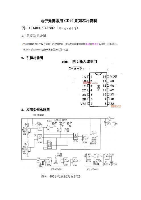
例:CD4001/74LS02(四双输入或非门)1、简要功能介绍2、引脚功能图3、应用实例电路图图* 4001构成视力保护器例:CD4011/74LS08(四2输入端与非门)1、引脚功能图逻辑表达式:Y = A.B(1)当X=0、Y=0时,将使两个NAND门之输出均为1,违反触发器之功用,故禁止使用。
如真值表第一列。
(2)当X=0、Y=1时,由于X=1导致NAND-A的输出为”1”,使得NAND-B的两个输入均为”1”,因此NAND-B的输出为”0”,如真值表第二列。
(3)当X=1、Y=0时,由于Y=0导致NAND-B的输出为”1”,使得NAND-1的两个输入均为””1,因此NAND-A的输出为”0”,如真值表第三列。
(4)当X=1、Y=1时,因为一个””1不影响NAND门的输出,所以两个NAND门的输出均不改变状态,如真值表第四列。
3、应用实例电路图例:CD4012/74LS20(双4输入端与非门)例:CD4017/CD4022(十进制计数/分配器)1、简要功能介绍CD4017 是5 位Johnson 计数器,具有10 个译码输出端,CP、CR、INH 输入端。
时钟输cd4017入端的斯密特触发器具有脉冲整形功能,对输入时钟脉冲上升和下降时间无限制。
INH 为低电平时,计数器在时钟上升沿计数;反之,计数功能无效。
CR 为高电平时,计数器清零。
2、引脚功能图CO:进位脉冲输出CP:时钟输入端CR:清除端INH:禁止端Q0-Q9 计数脉冲输出端VDD:正电源VSS:地3、应用实例电路图例:CD4026(十进制计数/7段译码器)1、引脚功能图当2和15为低3为高时,数码管随脉冲0-1-2…9-02脚为高电平时计数锁存脚5.4.14一般为高显9时5脚为低显2时14脚为低4脚与3脚一至3、应用实例电路图图* 4026构成时基电路例:CD4027/74LS111、114(双J-K触发器)1、引脚功能图当jk同时为1时Qn+1=Qn’3、应用实例电路图该振荡器能产生交变的50Hz脉冲方波,其占空比为50%。
ADS7868IDBVRG4资料

BurrĆBrown Products from TexasInstrumentsFEATURESAPPLICATIONSDESCRIPTIONVINCS SCLK SDOADS7866ADS7867ADS7868SLAS465–JUNE 20051.2-V,12-/10-/8-BIT,200-KSPS/100-KSPS,MICRO-POWER,MINIATURE ANALOG-TO-DIGITAL CONVERTER WITH SERIAL INTERFACEThe sampling,conversion,and activation of digital output SDO are initiated on the falling edge of CS.•Single 1.2-V to 3.6-V Supply Operation The serial clock SCLK is used for controlling the •High Throughputconversion rate and shifting data out of the converter.Furthermore,SCLK provides a mechanism to allow –200/240/280KSPS for 12/10/8-Bit V DD ≥1.6V digital host processors to synchronize with the con-–100/120/140KSPS for 12/10/8-Bit V DD ≥1.2V verter.These converters interface with •±1.5LSB INL,12-Bit NMC (ADS7866)micro-processors or DSPs through a high-speed SPI •71dB SNR,–83dB THD at f IN =30kHz compatible serial interface.There are no pipeline delays associated with the device.(ADS7866)•Synchronized Conversion with SCLK The minimum conversion time is determined by the frequency of the serial clock input,SCLK,while the •SPI Compatible Serial Interface maximum frequency of SCLK is determined by the •No Pipeline Delays minimum sampling time required to charge the input •Low Powercapacitance to 12/10/8-bit accuracy for the ADS7866/67/68,respectively.The maximum –1.39mW Typ at 200KSPS,V DD =3.6V throughput is determined by how often a conversion –0.39mW Typ at 200KSPS,V DD =1.6V is initiated when the minimum sampling time is met –0.22mW Typ at 100KSPS,V DD =1.2V and the maximum SCLK frequency is used.Each •Auto Power-Down:8nA Typ,300nA Max device automatically powers down after each conver-sion,which allows each device to save power when •0V to V DD Unipolar Input Range the throughput is reduced while using the maximum •6-Pin SOT-23PackageSCLK frequency.The converter reference is taken internally from the supply.Hence,the analog input range for these •Battery Powered Systems devices is 0V to V DD .•Isolated Data Acquisition These devices are available in a 6-pin SOT-23•Medical Instrumentspackage and are characterized over the industrial •Portable Communication–40°C to 85°C temperature range.•Portable Data Acquisition Systems •Automatic Test EquipmentThe ADS7866/67/68are low power,miniature,12/10/8-bit A/D converters each with a unipolar,single-ended input.These devices can operate from a single 1.6V to 3.6V supply with a 200-KSPS throughput for ADS7866.In addition,these devices can maintain at least a 100-KSPS throughput with a supply as low as 1.2V.Micro-Power Miniature SAR Converter FamilyRESOLUTION/SPEED <200KSPS1MSPS –1.25MSPS12-Bit ADS7866(1.2V DD to 3.6V DD )ADS7886(2.35V DD to 5.25V DD )10-Bit ADS7867(1.2V DD to 3.6V DD )ADS7887(2.35V DD to 5.25V DD )8-BitADS7868(1.2V DD to 3.6V DD )ADS7888(2.35V DD to 5.25V DD )Please be aware that an important notice concerning availability,standard warranty,and use in critical applications of Texas Instruments semiconductor products and disclaimers thereto appears at the end of this data sheet.PRODUCTION DATA information is current as of publication date.Copyright ©2005,Texas Instruments IncorporatedProducts conform to specifications per the terms of the Texas Instruments standard warranty.Production processing does not necessarily include testing of all parameters.元器件交易网ABSOLUTE MAXIMUM RATINGSADS7866ADS7867ADS7868SLAS465–JUNE 2005These devices have limited built-in ESD protection.The leads should be shorted together or the device placed in conductive foam during storage or handling to prevent electrostatic damage to the MOS gates.ORDERING INFORMATION (1)MAXIMUM MAXIMUM NO MISSING PACKAGE SPECIFIED TRANSPORT INTEGRAL DIFFERENTIAL CODES PACKAGE PACKAGE ORDERING MODELMARKING TEMPERATUREMEDIA,LINEARITY LINEARITY RESOLULTIONTYPE DESIGNATORNUMBER (SYMBOL)RANGE QUANTITY (LSB)(LSB)(BIT)ADS7866I ±1.5–1/+1.512SOT23-6A66Y DBV –40°C to 85°C ADS7866IDBVT Small tape and reel,250ADS7866I ±1.5–1/+1.512SOT23-6A66Y DBV –40°C to 85°C ADS7866IDBVR Tape and reel,3000ADS7867I ±0.5±0.510SOT23-6A67Y DBV –40°C to 85°C ADS7867IDBVT Small tape and reel,250ADS7867I ±0.5±0.510SOT23-6A67Y DBV –40°C to 85°C ADS7867IDBVR Tape and reel,3000ADS7868I ±0.5±0.58SOT23-6A68Y DBV –40°C to 85°C ADS7868IDBVT Small tape and reel,250ADS7868I±0.5±0.58SOT23-6A68YDBV–40°C to 85°CADS7868IDBVRTape and reel,3000(1)For the most current package and ordering information,see the Package Option Addendum at the end of this document,or see the TI web site at .over operating free-air temperature range (unless otherwise noted)RATINGV DD to GND–0.3V to 4.0V Analog input voltage to GND –0.3V to V DD +0.3V Digital input voltage to GND –0.3V to 4.0V Digital output voltage to GND–0.3V to V DD +0.3VT AOperating free-air temperature range –40°C to 85°C T STORAGE Storage temperature range –65°C to 150°CT JJunction temperature 150°C θJA Thermal impedance 110.9°C/W SOT-23Package θJC Thermal impedance 22.31°C/W Vapor phase (10–40sec)250°C Lead temperature,soldering Infrared (10–30sec)260°C ESD3kV2元器件交易网 SPECIFICATIONS,ADS7866ADS7866ADS7867ADS7868 SLAS465–JUNE2005At–40°C to85°C,fSAMPLE =200KSPS and fSCLK=3.4MHz if1.6V≤VDD≤3.6V;f SAMPLE=100KSPS and f SCLK=1.7MHz if1.2V≤VDD<1.6V(unless otherwise noted)PARAMETER TEST CONDITIONS MIN TYP MAX UNIT SYSTEM PERFORMANCEResolution12BitsNo missing codes12BitsIntegral linearity–1.5 1.5LSB(1)Differential linearity–1 1.5LSB1.2V≤V DD<1.6V–22Offset error(2)LSB1.6V≤V DD≤3.6V–331.2V≤V DD<1.6V–22Gain error(3)LSB1.6V≤V DD≤3.6V–221.2V≤V DD<1.6V–2.5 2.5Total unadjusted error(4)LSB1.6V≤V DD≤3.6V–3.5 3.5SAMPLING DYNAMICS(See Timing Characteristics Section)t CONVERT Conversion time f SCLK=3.4MHz,13SCLK cycles 3.82µst SAMPLE Acquisition time f SCLK=3.4MHz,1.6V≤V DD≤3.6V0.64µsf SAMPLE Throughput rate f SCLK=3.4MHz,1.6V≤V DD≤3.6V200KSPSAperture delay10nsAperture jitter40ps DYNAMIC CHARACTERISTICSf IN=30kHz,1.2V≤V DD<1.6V68Signal-to-noiseSINAD dB and distortion fIN=30kHz,1.6V≤V DD≤3.6V6970f IN=30kHz,1.2V≤V DD<1.6V70SNR Signal-to-noise ratio dBf IN=30kHz,1.6V≤V DD≤3.6V7071f IN=30kHz,1.2V≤V DD<1.6V–70THD Total harmonic distortion(5)dBf IN=30kHz,1.6V≤V DD≤3.6V–83f IN=30kHz,1.2V≤V DD<1.6V75Spurious free dynamicSFDR dB range fIN=30kHz,1.6V≤V DD≤3.6V85At0.1dB,1.2V≤V DD<1.6V2At0.1dB,1.6V≤V DD≤3.6V4Full-power bandwidth(6)MHzAt3dB,1.2V≤V DD<1.6V3At3dB,1.6V≤V DD≤3.6V8 ANALOG INPUTFull-scale input span(7)VIN–GND0V DD VC S Input capacitance12pFInput leakage current–11µA DIGITAL INPUTLogic family,CMOS1.2V≤V DD<1.6V0.7×V DD 3.61.6V≤V DD<1.8V0.7×V DD 3.6V IH Input logic high level V1.8V≤V DD<2.5V0.7×V DD3.62.5V≤V DD≤3.6V2 3.6(1)LSB=Least Significant BIt(2)The difference in the first code transition000...000to000...001from the ideal value of GND+1LSB.(3)The difference in the last code transition011...111to111...111from the ideal value of V DD-1LSB with the offset error removed.(4)The absolute difference from the ideal transfer function of the converter.This specification is similar to INL error except the effects ofoffset error and gain error are included.(5)The2nd through10th harmonics are used to determine THD.(6)Input frequency where the amplitude of the digitized signal has decreased by0.1dB or3dB.(7)Ideal input span which does not include gain or offset errors.3元器件交易网ADS7866ADS7867ADS7868SLAS465–JUNE 2005SPECIFICATIONS,ADS7866(continued)At –40°C to 85°C,f SAMPLE =200KSPS and f SCLK =3.4MHz if 1.6V ≤V DD ≤3.6V;f SAMPLE =100KSPS and f SCLK =1.7MHz if 1.2V ≤V DD <1.6V (unless otherwise noted)PARAMETERTEST CONDITIONSMIN TYPMAX UNIT1.2V ≤V DD <1.6V–0.20.2×V DD 1.6V ≤V DD <1.8V –0.20.2×V DD V ILInput logic low levelV 1.8V ≤V DD <2.5V –0.20.3×V DD2.5V ≤V DD ≤3.6V–0.20.8I SCLK SCLK pin leakage current Digital input =0V or V DD–10.021µA I CS CS pin leakage current ±1µA C IN Digital input pin capacitance 10pF DIGITAL OUTPUTV OH Output logic high level I SOURCE =200µA V DD –0.2V DD V V OL Output logic low level I SINK =200µA 00.2V I SDO SDO pin leakage current Floating output –11µA Digital output pin C OUTFloating output10pF capacitanceData format,straight binaryPOWER SUPPLY REQUIREMENTS V DDSupply voltage1.23.6Vf SAMPLE =200KSPS,f SCLK =3.4MHz,V DD =3.6V 385500f SAMPLE =100KSPS,f SCLK =3.4MHz,V DD =3.6V 193µA f SAMPLE =50KSPS,f SCLK =3.4MHz,V DD =3.6V 97f SAMPLE =20KSPS,f SCLK =3.4MHz,V DD =3.6V 39f SAMPLE =200KSPS,f SCLK =3.4MHz,V DD =3V 340f SAMPLE =100KSPS,f SCLK =3.4MHz,V DD =3V 170µAf SAMPLE =50KSPS,f SCLK =3.4MHz,V DD =3V 85f SAMPLE =20KSPS,f SCLK =3.4MHz,V DD =3V 35f SAMPLE =200KSPS,f SCLK =3.4MHz,V DD =2.5V 305f SAMPLE =100KSPS,f SCLK =3.4MHz,V DD =2.5V153µA f SAMPLE =50KSPS,f SCLK =3.4MHz,V DD =2.5V 77Supply current,Digital inputs =0V I DDf SAMPLE =20KSPS,f SCLK =3.4MHz,V DD =2.5V 31normal operationor V DDf SAMPLE =200KSPS,f SCLK =3.4MHz,V DD =1.8V 256f SAMPLE =100KSPS,f SCLK =3.4MHz,V DD =1.8V 128µA f SAMPLE =50KSPS,f SCLK =3.4MHz,V DD =1.8V 65f SAMPLE =20KSPS,f SCLK =3.4MHz,V DD =1.8V 26f SAMPLE =200KSPS,f SCLK =3.4MHz,V DD =1.6V 241330f SAMPLE =100KSPS,f SCLK =3.4MHz,V DD =1.6V 121µA f SAMPLE =50KSPS,f SCLK =3.4MHz,V DD =1.6V 61f SAMPLE =20KSPS,f SCLK =3.4MHz,V DD =1.6V 25f SAMPLE =100KSPS,f SCLK =1.7MHz,V DD =1.2V 186250f SAMPLE =50KSPS,f SCLK =1.7MHz,V DD =1.2V 93µAf SAMPLE =20KSPS,f SCLK =1.7MHz,V DD =1.2V37I DDPower-down modeSCLK on or off0.0080.3µAPOWER DISSIPATIONf SAMPLE =200KSPS,f SCLK =3.4MHz,V DD =3.6V1.39 1.80Normal operation f SAMPLE =200KSPS,f SCLK =3.4MHz,V DD =1.6V 0.390.53mWf SAMPLE =100KSPS,f SCLK =1.7MHz,V DD =1.2V 0.220.3Power-down modeSCLK on or off,V DD =3.6V1.08µW TEMPERATURE RANGESpecified performance–4085°C4元器件交易网 SPECIFICATIONS,ADS7867ADS7866ADS7867ADS7868 SLAS465–JUNE2005At–40°C to85°C,fSAMPLE =240KSPS and fSCLK=3.4MHz if1.6V≤VDD≤3.6V;f SAMPLE=120KSPS and f SCLK=1.7MHz if1.2V≤VDD<1.6V(unless otherwise noted)PARAMETER TEST CONDITIONS MIN TYP MAX UNIT SYSTEM PERFORMANCEResolution10BitsNo missing codes10BitsIntegral linearity–0.50.5LSB(1)Differential linearity–0.50.5LSB1.2V≤V DD<1.6V–0.750.75Offset error(2)LSB1.6V≤V DD≤3.6V–111.2V≤V DD<1.6V–0.50.5Gain error(3)LSB1.6V≤V DD≤3.6V–0.50.51.2V≤V DD<1.6V–22Total unadjusted error(4)LSB1.6V≤V DD≤3.6V–22SAMPLING DYNAMICS(See Timing Characteristics Section)t CONVERT Conversion time f SCLK=3.4MHz,11SCLK cycles 3.235µst SAMPLE Acquisition time f SCLK=3.4MHz,1.6V≤V DD≤3.6V0.64µsf SAMPLE Throughput rate f SCLK=3.4MHz,1.6V≤V DD≤3.6V240KSPSAperture delay10nsAperture jitter40ps DYNAMIC CHARACTERISTICSf SAMPLE=100KSPS,f IN=30kHz,1.2V≤V DD<1.6V61Signal-to-noiseSINAD dB and distortion fSAMPLE=200KSPS,f IN=30kHz,1.6V≤V DD≤3.6V6161.7f SAMPLE=100KSPS,f IN=30kHz,1.2V≤V DD<1.6V61.5SNR Signal-to-noise ratio dBf SAMPLE=200KSPS,f IN=30kHz,1.6V≤V DD≤3.6V61.8f SAMPLE=100KSPS,f IN=30kHz,1.2V≤V DD<1.6V-68THD Total harmonic distortion(5)dBf SAMPLE=200KSPS,f IN=30kHz,1.6V≤V DD≤3.6V-78-72f SAMPLE=100KSPS,f IN=30kHz,1.2V≤V DD<1.6V73SFDR Spurious free dynamic range dBf SAMPLE=200KSPS,f IN=30kHz,1.6V≤V DD≤3.6V7480At0.1dB,1.2V≤V DD<1.6V2At0.1dB,1.6V≤V DD≤3.6V4Full-power bandwidth(6)MHzAt3dB,1.2V≤V DD<1.6V3At3dB,1.6V≤V DD≤3.6V8 ANALOG INPUTFull-scale input span(7)VIN–GND0V DD VC S Input capacitance12pFInput leakage current–11µA DIGITAL INPUTLogic family,CMOS1.2V≤V DD<1.6V0.7×V DD 3.61.6V≤V DD<1.8V0.7×V DD 3.6V IH Input logic high level V1.8V≤V DD<2.5V0.7×V DD3.62.5V≤V DD≤3.6V2 3.6(1)LSB=Least Significant BIt(2)The difference in the first code transition000...000to000...001from the ideal value of GND+1LSB.(3)The difference in the last code transition011...111to111...111from the ideal value of V DD-1LSB with the offset error removed.(4)The absolute difference from the ideal transfer function of the converter.This specification is similar to INL error except the effects ofoffset error and gain error are included.(5)The2nd through10th harmonics are used to determine THD.(6)Input frequency where the amplitude of the digitized signal has decreased by0.1dB or3dB.(7)Ideal input span which does not include gain or offset errors.5元器件交易网ADS7866ADS7867ADS7868SLAS465–JUNE 2005SPECIFICATIONS,ADS7867(continued)At –40°C to 85°C,f SAMPLE =240KSPS and f SCLK =3.4MHz if 1.6V ≤V DD ≤3.6V;f SAMPLE =120KSPS and f SCLK =1.7MHz if 1.2V ≤V DD <1.6V (unless otherwise noted)PARAMETERTEST CONDITIONSMIN TYPMAX UNIT1.2V ≤V DD <1.6V–0.20.2×V DD 1.6V ≤V DD <1.8V –0.20.2×V DD V ILInput logic low levelV 1.8V ≤V DD <2.5V –0.20.3×V DD2.5V ≤V DD ≤3.6V–0.20.8I SCLK SCLK pin leakage current Digital input =0V or V DD–10.021µA I CS CS pin leakage current ±1µA C IN Digital input pin capacitance 10pF DIGITAL OUTPUTV OH Output logic high level I SOURCE =200µA V DD –0.2V DD V V OL Output logic low level I SINK =200µA 00.2V I SDO SDO pin leakage current Floating output –11µA Digital output pin C OUTFloating output10pF capacitanceData format,straight binaryPOWER SUPPLY REQUIREMENTS V DDSupply voltage1.23.6V f SAMPLE =240KSPS,f SCLK =3.4MHz,V DD =3.6V 420500µA f SAMPLE =100KSPS,f SCLK =3.4MHz,V DD =3.6V172f SAMPLE =240KSPS,f SCLK =3.4MHz,V DD =1.6V 261330Supply current,Digital Inputs =0V I DDµA normal operationor V DD f SAMPLE =100KSPS,f SCLK =3.4MHz,V DD =1.6V107f SAMPLE =120KSPS,f SCLK =1.7MHz,V DD =1.2V 202250µA f SAMPLE =50KSPS,f SCLK =1.7MHz,V DD =1.2V83I DDPower-down modeSCLK on or off0.0080.3µAPOWER DISSIPATIONf SAMPLE =240KSPS,f SCLK =3.4MHz,V DD =3.6V1.51 1.80Normal operation f SAMPLE =240KSPS,f SCLK =3.4MHz,V DD =1.6V 0.420.53mWf SAMPLE =120KSPS,f SCLK =1.7MHz,V DD =1.2V 0.240.30Power-down modeSCLK on or off,V DD =3.6V1.08µW TEMPERATURE RANGESpecified performance–4085°C6元器件交易网 SPECIFICATIONS,ADS7868ADS7866ADS7867ADS7868 SLAS465–JUNE2005At–40°C to85°C,fSAMPLE =280KSPS and fSCLK=3.4MHz if1.6V≤VDD≤3.6V;f SAMPLE=140KSPS and f SCLK=1.7MHz if1.2V≤VDD<1.6V(unless otherwise noted)PARAMETER TEST CONDITIONS MIN TYP MAX UNIT SYSTEM PERFORMANCEResolution8BitsNo missing codes8BitsIntegral linearity–0.50.5LSB(1)Differential linearity–0.50.5LSB1.2V≤V DD<1.6V–0.50.5Offset error(2)LSB1.6V≤V DD≤3.6V–0.50.51.2V≤V DD<1.6V–0.50.5Gain error(3)LSB1.6V≤V DD≤3.6V–0.50.51.2V≤V DD<1.6V–11Total unadjusted error(4)LSB1.6V≤V DD≤3.6V–11SAMPLING DYNAMICS(See Timing Characteristics Section)t CONVERT Conversion time f SCLK=3.4MHz,9SCLK cycles 2.647µst SAMPLE Acquisition time f SCLK=3.4MHz,1.6V≤V DD≤3.6V0.64µsf SAMPLE Throughput rate f SCLK=3.4MHz,1.6V≤V DD≤3.6V280KSPSAperture delay10nsAperture jitter40ps DYNAMIC CHARACTERISTICSf SAMPLE=100KSPS,f IN=30kHz,1.2V≤V DD<1.6V49Signal-to-noiseSINAD dB and distortion fSAMPLE=200KSPS,f IN=30kHz,1.6V≤V DD≤3.6V4949.4f SAMPLE=100KSPS,f IN=30kHz,1.2V≤V DD<1.6V49.4SNR Signal-to-noise ratio dBf SAMPLE=200KSPS,f IN=30kHz,1.6V≤V DD≤3.6V49.8f SAMPLE=100KSPS,f IN=30kHz,1.2V≤V DD<1.6V–65Total harmonicTHD dB distortion(5)fSAMPLE=200KSPS,f IN=30kHz,1.6V≤V DD≤3.6V–72-66f SAMPLE=100KSPS,f IN=30kHz,1.2V≤V DD<1.6V67Spurious free dynamicSFDR dB range fSAMPLE=200KSPS,f IN=30kHz,1.6V≤V DD≤3.6V6667At0.1dB,1.2V≤V DD<1.6V2At0.1dB,1.6V≤V DD≤3.6V4Full-power bandwidth(6)MHzAt3dB,1.2V≤V DD<1.6V3At3dB,1.6V≤V DD≤3.6V8 ANALOG INPUTFull-scale input span(7)VIN–GND0V DD VC S Input capacitance12pFInput leakage current–11µA DIGITAL INPUTLogic family,CMOS1.2V≤V DD<1.6V0.7×V DD 3.61.6V≤V DD<1.8V0.7×V DD 3.6V IH Input logic high level V1.8V≤V DD<2.5V0.7×V DD3.62.5V≤V DD≤3.6V2 3.6(1)LSB=Least Significant BIt(2)The difference in the first code transition000...000to000...001from the ideal value of GND+1LSB.(3)The difference in the last code transition011...111to111...111from the ideal value of V DD-1LSB with the offset error removed.(4)The absolute difference from the ideal transfer function of the converter.This specification is similar to INL error except the effects ofoffset error and gain error are included.(5)The2nd through10th harmonics are used to determine THD.(6)Input frequency where the amplitude of the digitized signal has decreased by0.1dB or3dB.(7)Ideal input span which does not include gain or offset errors.7元器件交易网ADS7866ADS7867ADS7868SLAS465–JUNE 2005SPECIFICATIONS,ADS7868(continued)At –40°C to 85°C,f SAMPLE =280KSPS and f SCLK =3.4MHz if 1.6V ≤V DD ≤3.6V;f SAMPLE =140KSPS and f SCLK =1.7MHz if 1.2V ≤V DD <1.6V (unless otherwise noted)PARAMETERTEST CONDITIONSMIN TYPMAX UNIT1.2V ≤V DD <1.6V–0.20.2×V DD 1.6V ≤V DD <1.8V –0.20.2×V DD V ILInput logic low levelV 1.8V ≤V DD <2.5V –0.20.3×V DD2.5V ≤V DD ≤3.6V–0.20.8I SCLK SCLK pin leakage current Digital input =0V or V DD –10.021µA I CS CS pin leakage current ±1µA Digital input pin C IN10pF capacitanceDIGITAL OUTPUT V OH Output logic high level I SOURCE =200µA V DD –0.2V DD V V OL Output logic low level I SINK =200µA 00.2V I SDO SDO pin leakage current Floating output –11µA Digital output pin C OUTFloating output10pFcapacitance Data format,straight binaryPOWER SUPPLY REQUIREMENTS V DDSupply voltage1.23.6V f SAMPLE =280KSPS,f SCLK =3.4MHz,V DD =3.6V 439500µA f SAMPLE =100KSPS,f SCLK =3.4MHz,V DD =3.6V154f SAMPLE =280KSPS,f SCLK =3.4MHz,V DD =1.6V 264330Supply current,Digital Inputs =0V I DDµA normal operationor V DD f SAMPLE =100KSPS,f SCLK =3.4MHz,V DD =1.6V93f SAMPLE =140KSPS,f SCLK =1.7MHz,V DD =1.2V 201250µA f SAMPLE =50KSPS,f SCLK =1.7MHz,V DD =1.2V70I DDPower-down modeSCLK on or off0.0080.3µAPOWER DISSIPATIONf SAMPLE =280KSPS,f SCLK =3.4MHz,V DD =3.6V1.58 1.8Normal operation f SAMPLE =280KSPS,f SCLK =3.4MHz,V DD =1.6V 0.420.53mWf SAMPLE =140KSPS,f SCLK =1.7MHz,V DD =1.2V 0.240.3Power-down modeSCLK on or off,V DD =3.6V1.08µW TEMPERATURE RANGESpecified performance–4085°C8元器件交易网TIMING REQUIREMENTS (1)(2)ADS7866ADS7867ADS7868SLAS465–JUNE 2005At –40°C to 85°C,f SCLK =3.4MHz if 1.6V ≤V DD ≤3.6V;f SCLK =1.7MHz if 1.2V ≤V DD <1.6V,50-pF Load on SDO Pin,unless otherwise notedPARAMETERTEST CONDITIONS MIN TYPMAX UNIT t sample Sample timet SU(CSF-FSCLKF)+2×t C(SCLK)µs ADS786613×t C(SCLK)t convertConversion timeADS786711×t C(SCLK)µsADS78689×t C(SCLK)1.2V ≤V DD <1.6VSee (3)1001.6V ≤V DD <1.8V See (3)100t C(SCLK)Cycle timeµs1.8V ≤V DD <2.5V See (3)502.5V ≤V DD ≤3.6VSee(3)6.7t WH(SCLK)Pulse duration 0.4×t C(SCLK)0.6×t C(SCLK)ns t WL(SCLK)Pulse duration0.4×t C(SCLK)0.6×t C(SCLK)ns 1.2V ≤V DD <1.6V192t SU(CSF-FSCLKF)Setup time1.6V ≤V DD <1.8V 55ns1.8V ≤V DD ≤3.6V 551.2V ≤V DD <1.6V65t D(CSF-SDOVALID)Delay time1.6V ≤V DD <1.8V 55ns 1.8V ≤V DD ≤3.6V 551.2V ≤V DD <1.6V20t H(SCLKF-SDOVALID)Hold time1.6V ≤V DD <1.8V 10ns1.8V ≤V DD ≤3.6V 101.2V ≤V DD <1.6V140t D(SCLKF-SDOVALID)Delay time1.6V ≤V DD <1.8V 140ns 1.8V ≤V DD ≤3.6V 1401.2V ≤V DD <1.6V1080t DIS(EOC-SDOZ)Disable time1.6V ≤V DD <1.8V 760ns 1.8V ≤V DD ≤3.6V 7601.2V ≤V DD <1.6V20t WH(CS)Pulse duration1.6V ≤V DD <1.8V 10ns1.8V ≤V DD ≤3.6V 101.2V ≤V DD <1.6V20t SU(LSBZ-CSF)Setup time1.6V ≤V DD <1.8V 10ns 1.8V ≤V DD ≤3.6V10(1)All input signals are specified with t r =t f =5ns (10%to 90%of V DD )and timed from a voltage level of (V IL +V IH )/2.(2)See timing diagram in Figure 1.(3)Min t C(SCLK)is Min t SAMPLE of the specific resolution and supply voltage.See Acquisition Time,Conversion Time,and Total Cycle Time section for further details.Figure 1.Timing Diagram9元器件交易网PINCONFIGURATION(TOP VIEW)REF/V DDGND VINSCLKADS7866/67/68DBV PACKAGE CS SDO ADS7866ADS7867ADS7868SLAS465–JUNE 2005TERMINAL FUNCTIONSTERMINAL DESCRIPTIONNAME NO.REF/V DD 1External reference input and power supplyGND 2Ground for signal and power supply.All analog and digital signals are referred with respect to this pin.VIN 3Analog signal inputSCLK 4Serial clock input.This clock is used for clocking data out,and it is the source of conversion clock.This is the serial data output of the conversion result.The serial stream comes with MSB first.The MSB is clocked out (changed)on the falling edge one SCLK after the sampling period ends.This results in four leading zeros after CS SDO5becomes active.SDO is 3-stated once all the valid bits are clocked out (12for ADS7866,10for ADS7867,and 8for ADS7868).This is an active low input signal.It is used as a chip select to gate the SCLK input,to initiate a conversion,and to CS 6frame output data.10元器件交易网TYPICAL CHARACTERISTICS ADS7866f i − Input Frquency − kHzN o r m a l i z e d A m p l i t u d e − d B05101520253035404550f i − Input Frquency − kHzN o r m a l i z e d A m p l i t u d e − dBf i − Input Frequency − kHzT H D − T o t a l H a r m o n i c D i s t o r t i o n − d Bf i − Input Frequency − kHzS N R − S i g n a l -t o -N o i s e R a t i o − d Bf i − Input Frequency − kHzS I N A D − S i g n a l -t o -N o i s e a n d D i s t o r t i o n − d BFFT (8192Points)Figure 2.FFT (8192Points)Figure 3.SIGNAL-TO-NOISE RATIOSIGNAL-TO-NOISE TOTAL HARMONIC DISTORTIONvsAND DISTORTIONvsINPUT FREQUENCYvsINPUT FREQUENCYINPUT FREQUENCYFigure 4.Figure 5.Figure 6.f i − Input Frequency − kHzS F D R − S p u r i o u s F r e e D y n a m i c R a n g e − dBSCLK Frequency − MHzC C I S u p p l y C u r r e n t − −AµV DD − Supply Voltage − VC C I S u p p l y C u r r e n t − −AµThroughput − KSPSP o w e r C o n s u m p t i o n − m Wf i − Input Frequency − kHzT H D − T o t a l H a r m o n i c D i s t o r t i o n − dBCodeI N L − L S B s(Straight Binary in Decimal)SPURIOUS FREE DYNAMIC RANGESUPPLY CURRENTSUPPLY CURRENTvsvsvsINPUT FREQUENCYSCLK FREQUENCYSUPPLY VOLTAGEFigure 7.Figure 8.Figure 9.POWER CONSUMPTIONTOTAL HARMONIC DISTORTIONvsvsTHROUGHPUTINPUT FREQUENCYFigure 10.Figure 11.Figure 12.00.20.40.60.81CodeD N L − L S B s(Straight Binary in Decimal)−1−0.8−0.6−0.4−0.200.20.40.60.8105121024153620482560307235844096CodeI N L − L S B s(Straight Binary in Decimal)CodeD N L − L S B s(Straight Binary in Decimal)DNLFigure 13.INLFigure 14.DNLFigure 15.V DD − Supply Voltage − VC C I S u p p l y C u r r e n t − −AµV DD − Supply Voltage − VT h r o u g h p u t R a t e − K S P SV DD − Supply Voltage − VT h r o u g h p u t R a t e − K S P SMAX SUPPLY CURRENTTHROUGHPUT RATETHROUGHPUT RATEvsvsvsSUPPLY VOLTAGESUPPLY VOLTAGESUPPLY VOLTAGEFigure 16.Figure 17.Figure 18.f i − Input Frequency − kHzN o r m a l i z e d A m p l i t u d e − d BN o r m a l i z e d A m p l i t u d e − d Bf i− Input Frequency − kHzV DD − Supply Voltage − VT h r o u g h p u t R a t e − K S P S1.21.4 1.6 1.8V DD − Supply Voltage − VT h r o u g h p u t R a t e − K S P SFFT (8192Points)Figure 19.FFT (8192Points)Figure 20.THROUGHPUT RATETHROUGHPUT RATEvsvsSUPPLY VOLTAGESUPPLY VOLTAGEFigure 21.Figure 22.N o r m a l i z e d A m p l i t u d e − d Bf i− Input Frequency − kHzN o r m a l i z e d A m p l i t u d e − d Bf i − Input Frequency − kHzV DD − Supply Voltage − VT h r o u g h p u t R a t e − K S P SV DD − Supply Voltage − VT h r o u g h p u t R a t e − K S P SFFT (8192Points)Figure 23.FFT (8192Points)Figure 24.THROUGHPUT RATETHROUGHPUT RATEvsvsSUPPLY VOLTAGESUPPLY VOLTAGEFigure 25.Figure 26.THEORY OF OPERATIONThe ADS7866/67/68is a family of low supply voltage,low power,high-speed successive approximation register (SAR)analog-to-digital converters(ADCs).The devices can be operated from a supply range from1.2V to3.6 V.There is no need for an external reference.The reference is derived internally from the supply voltage,so the analog input range can be from0V to V DD.These ADCs use a charge redistribution architecture,which inherently includes a sample/hold function.START OF A CONVERSION CYCLEA conversion cycle is initiated by bringing the CS pin low and supplying the serial clock SCLK.The time between the falling edge of CS and the third falling edge of SCLK after CS falls is used to acquire the input signal.This must be greater than or equal to the minimum acquisition time(MIN t SAMPLE in Table1)specified for the desired resolution and supply voltage.On the third falling edge of SCLK after CS goes into hold mode and the process of digitizing the sampled input signal starts.Acquisition Time,Conversion Time,and Total Cycle TimeThe maximum SCLK frequency is determined by the minimum acquisition time(MIN t SAMPLE)specified for the specific resolution and supply voltage of the device.The conversion time is determined by the frequency of SCLK since this is a synchronous converter.The conversion time is13times the SCLK cycle time t C(SCLK)for the ADS7866,11times for the ADS7867,and9times for the ADS7868.The acquisition time,which is also the power up time,is the set-up time between the first falling edge of SCLK after CS falls(t SU(CSF-FSCLKF))plus2 times t C(SCLK).The total cycle time,t CYCLE,which is the inverse of the maximum sample rate,can be calculated as follows: t CYCLE=t SAMPLE+t CONVERT+0.5×t C(SCLK)if t DIS(EOC-SDOZ)+t SU(LSBZ-CSF)≤0.5×t C(SCLK)t CYCLE=t SAMPLE+t CONVERT+t DIS(EOC-SDOZ)+t SU(LSBZ-CSF)if t DIS(EOC-SDOZ)+t SU(LSBZ-CSF)>0.5×t C(SCLK)。
- 1、下载文档前请自行甄别文档内容的完整性,平台不提供额外的编辑、内容补充、找答案等附加服务。
- 2、"仅部分预览"的文档,不可在线预览部分如存在完整性等问题,可反馈申请退款(可完整预览的文档不适用该条件!)。
- 3、如文档侵犯您的权益,请联系客服反馈,我们会尽快为您处理(人工客服工作时间:9:00-18:30)。
PACKAGING INFORMATIONOrderable Device Status(1)PackageType PackageDrawingPins PackageQtyEco Plan(2)Lead/Ball Finish MSL Peak Temp(3)CD4508BD3ACTIVE CDIP SB JD241TBD POST-PLATE N/A for Pkg Type CD4508BE ACTIVE PDIP N2415Pb-Free(RoHS)CU NIPDAU N/A for Pkg TypeCD4508BEE4ACTIVE PDIP N2415Pb-Free(RoHS)CU NIPDAU N/A for Pkg Type CD4508BF3A ACTIVE CDIP J241TBD Call TI N/A for Pkg Type CD4508BM ACTIVE SOIC DW2425Green(RoHS&no Sb/Br)CU NIPDAU Level-1-260C-UNLIMCD4508BM96ACTIVE SOIC DW242000Green(RoHS&no Sb/Br)CU NIPDAU Level-1-260C-UNLIMCD4508BM96E4ACTIVE SOIC DW242000Green(RoHS&no Sb/Br)CU NIPDAU Level-1-260C-UNLIMCD4508BM96G4ACTIVE SOIC DW242000Green(RoHS&no Sb/Br)CU NIPDAU Level-1-260C-UNLIMCD4508BME4ACTIVE SOIC DW2425Green(RoHS&no Sb/Br)CU NIPDAU Level-1-260C-UNLIMCD4508BMG4ACTIVE SOIC DW2425Green(RoHS&no Sb/Br)CU NIPDAU Level-1-260C-UNLIMCD4508BNSR ACTIVE SO NS242000Green(RoHS&no Sb/Br)CU NIPDAU Level-1-260C-UNLIMCD4508BNSRE4ACTIVE SO NS242000Green(RoHS&no Sb/Br)CU NIPDAU Level-1-260C-UNLIMCD4508BNSRG4ACTIVE SO NS242000Green(RoHS&no Sb/Br)CU NIPDAU Level-1-260C-UNLIMCD4508BPW ACTIVE TSSOP PW2460Green(RoHS&no Sb/Br)CU NIPDAU Level-1-260C-UNLIMCD4508BPWE4ACTIVE TSSOP PW2460Green(RoHS&no Sb/Br)CU NIPDAU Level-1-260C-UNLIMCD4508BPWG4ACTIVE TSSOP PW2460Green(RoHS&no Sb/Br)CU NIPDAU Level-1-260C-UNLIMCD4508BPWR ACTIVE TSSOP PW242000Green(RoHS&no Sb/Br)CU NIPDAU Level-1-260C-UNLIMCD4508BPWRE4ACTIVE TSSOP PW242000Green(RoHS&no Sb/Br)CU NIPDAU Level-1-260C-UNLIMCD4508BPWRG4ACTIVE TSSOP PW242000Green(RoHS&no Sb/Br)CU NIPDAU Level-1-260C-UNLIM(1)The marketing status values are defined as follows:ACTIVE:Product device recommended for new designs.LIFEBUY:TI has announced that the device will be discontinued,and a lifetime-buy period is in effect.NRND:Not recommended for new designs.Device is in production to support existing customers,but TI does not recommend using this part in a new design.PREVIEW:Device has been announced but is not in production.Samples may or may not be available.OBSOLETE:TI has discontinued the production of the device.(2)Eco Plan-The planned eco-friendly classification:Pb-Free(RoHS),Pb-Free(RoHS Exempt),or Green(RoHS&no Sb/Br)-please check /productcontent for the latest availability information and additional product content details.TBD:The Pb-Free/Green conversion plan has not been defined.Pb-Free(RoHS):TI's terms"Lead-Free"or"Pb-Free"mean semiconductor products that are compatible with the current RoHS requirements for all6substances,including the requirement that lead not exceed0.1%by weight in homogeneous materials.Where designed to be soldered at high temperatures,TI Pb-Free products are suitable for use in specified lead-free processes.Pb-Free(RoHS Exempt):This component has a RoHS exemption for either1)lead-based flip-chip solder bumps used between the die andpackage,or2)lead-based die adhesive used between the die and leadframe.The component is otherwise considered Pb-Free(RoHS compatible)as defined above.Green(RoHS&no Sb/Br):TI defines"Green"to mean Pb-Free(RoHS compatible),and free of Bromine(Br)and Antimony(Sb)based flame retardants(Br or Sb do not exceed0.1%by weight in homogeneous material)(3)MSL,Peak Temp.--The Moisture Sensitivity Level rating according to the JEDEC industry standard classifications,and peak solder temperature.Important Information and Disclaimer:The information provided on this page represents TI's knowledge and belief as of the date that it is provided.TI bases its knowledge and belief on information provided by third parties,and makes no representation or warranty as to the accuracy of such information.Efforts are underway to better integrate information from third parties.TI has taken and continues to take reasonable steps to provide representative and accurate information but may not have conducted destructive testing or chemical analysis on incoming materials and chemicals.TI and TI suppliers consider certain information to be proprietary,and thus CAS numbers and other limited information may not be available for release.In no event shall TI's liability arising out of such information exceed the total purchase price of the TI part(s)at issue in this document sold by TI to Customer on an annual basis.TAPE AND REEL INFORMATION*All dimensions are nominalDevicePackage Type Package Drawing Pins SPQReel Diameter (mm)Reel Width W1(mm)A0(mm)B0(mm)K0(mm)P1(mm)W (mm)Pin1Quadrant CD4508BM96SOIC DW 242000330.024.410.7515.7 2.712.024.0Q1CD4508BNSR SO NS 242000330.024.48.215.4 2.512.024.0Q1CD4508BPWRTSSOPPW242000330.016.46.958.31.68.016.0Q1*All dimensions are nominalDevice Package Type Package Drawing Pins SPQ Length(mm)Width(mm)Height(mm) CD4508BM96SOIC DW242000346.0346.041.0 CD4508BNSR SO NS242000346.0346.041.0 CD4508BPWR TSSOP PW242000346.0346.033.0元器件交易网IMPORTANT NOTICETexas Instruments Incorporated and its subsidiaries(TI)reserve the right to make corrections,modifications,enhancements,improvements, and other changes to its products and services at any time and to discontinue any product or service without notice.Customers should obtain the latest relevant information before placing orders and should verify that such information is current and complete.All products are sold subject to TI’s terms and conditions of sale supplied at the time of order acknowledgment.TI warrants performance of its hardware products to the specifications applicable at the time of sale in accordance with TI’s standard warranty.Testing and other quality control techniques are used to the extent TI deems necessary to support this warranty.Except where mandated by government requirements,testing of all parameters of each product is not necessarily performed.TI assumes no liability for applications assistance or customer product design.Customers are responsible for their products and applications using TI components.To minimize the risks associated with customer products and applications,customers should provide adequate design and operating safeguards.TI does not warrant or represent that any license,either express or implied,is granted under any TI patent right,copyright,mask work right, or other TI intellectual property right relating to any combination,machine,or process in which TI products or services are rmation published by TI regarding third-party products or services does not constitute a license from TI to use such products or services or a warranty or endorsement e of such information may require a license from a third party under the patents or other intellectual property of the third party,or a license from TI under the patents or other intellectual property of TI.Reproduction of TI information in TI data books or data sheets is permissible only if reproduction is without alteration and is accompanied by all associated warranties,conditions,limitations,and notices.Reproduction of this information with alteration is an unfair and deceptive business practice.TI is not responsible or liable for such altered rmation of third parties may be subject to additional restrictions.Resale of TI products or services with statements different from or beyond the parameters stated by TI for that product or service voids all express and any implied warranties for the associated TI product or service and is an unfair and deceptive business practice.TI is not responsible or liable for any such statements.TI products are not authorized for use in safety-critical applications(such as life support)where a failure of the TI product would reasonably be expected to cause severe personal injury or death,unless officers of the parties have executed an agreement specifically governing such use.Buyers represent that they have all necessary expertise in the safety and regulatory ramifications of their applications,and acknowledge and agree that they are solely responsible for all legal,regulatory and safety-related requirements concerning their products and any use of TI products in such safety-critical applications,notwithstanding any applications-related information or support that may be provided by TI.Further,Buyers must fully indemnify TI and its representatives against any damages arising out of the use of TI products in such safety-critical applications.TI products are neither designed nor intended for use in military/aerospace applications or environments unless the TI products are specifically designated by TI as military-grade or"enhanced plastic."Only products designated by TI as military-grade meet military specifications.Buyers acknowledge and agree that any such use of TI products which TI has not designated as military-grade is solely at the Buyer's risk,and that they are solely responsible for compliance with all legal and regulatory requirements in connection with such use. TI products are neither designed nor intended for use in automotive applications or environments unless the specific TI products are designated by TI as compliant with ISO/TS16949requirements.Buyers acknowledge and agree that,if they use any non-designated products in automotive applications,TI will not be responsible for any failure to meet such requirements.Following are URLs where you can obtain information on other Texas Instruments products and application solutions:Products ApplicationsAmplifiers AudioData Converters AutomotiveDSP BroadbandClocks and Timers Digital ControlInterface MedicalLogic MilitaryPower Mgmt Optical NetworkingMicrocontrollers SecurityRFID TelephonyRF/IF and ZigBee®Solutions Video&ImagingWirelessMailing Address:Texas Instruments,Post Office Box655303,Dallas,Texas75265Copyright©2008,Texas Instruments Incorporated。