5082-H153-0M000中文资料
5082-A808-KP000资料

Features• Low Power Consumption • Industry Standard Size• Industry Standard Pinout • Choice of Character Size7.6 mm (0.30 in), 10 mm (0.40 in), 10.9 mm (0.43 in), 14.2 mm (0.56 in), 20 mm (0.80 in)• Choice of ColorsAlGaAs Red, High Efficiency Red (HER), Yellow, Green• Excellent Appearance Evenly Lighted Segments±50° Viewing Angle• Design FlexibilityCommon Anode or Common CathodeSingle and Dual DigitLeft and Right Hand Decimal Points±1. Overflow Character• Categorized for Luminous IntensityYellow and Green Categorized for ColorUse of Like Categories Yields a Uniform Display• Excellent for Long Digit String Multiplexing DescriptionThese low current seven segment displays are designed for applica-tions requiring low power consumption. They are tested and selected for their excellent low current characteristics to ensure that the segments are matched at low currents. Drive currents as low as 1 mA per segment are available.Pin for pin equivalent displays are also available in a standard current or high light ambient design. The standard current displays are available in all colors and are ideal for most applica-tions. The high light ambient displays are ideal for sunlight ambients or long string lengths. For additional information see the 7.6 mm Micro Bright Seven Segment Displays, 10 mm Seven Segment Displays, 7.6 mm/10.9 mm Seven Segment Displays, 14.2 mm Seven Segment Displays, 20 mm Seven Segment Displays, or High Light Ambient Seven Segment Displays data sheets.Low Current Seven SegmentDisplays Technical Data HDSP-335x SeriesHDSP-555x SeriesHDSP-751x SeriesHDSP-A10x Series HDSP-A80x Series HDSP-A90x Series HDSP-E10x Series HDSP-F10x Series HDSP-G10x Series HDSP-H10x Series HDSP-K12x, K70x Series HDSP-N10x SeriesHDSP-N40x SeriesDevicesAlGaAs HER Yellow Green Package HDSP-HDSP-HDSP-HDSP-Description Drawing A1017511A801A9017.6 mm Common Anode Right Hand Decimal A A1037513A803A9037.6 mm Common Cathode Right Hand Decimal B A1077517A807A9077.6 mm Common Anode ±1. Overflow C A1087518A808A9087.6 mm Common Cathode ±1. Overflow D F10110 mm Common Anode Right Hand Decimal E F10310 mm Common Cathode Right Hand Decimal F F10710 mm Common Anode ±1. Overflow G F10810 mm Common Cathode ±1. Overflow H G10110 mm Two Digit Common Anode Right Hand Decimal X G10310 mm Two Digit Common Cathode Right Hand Decimal Y E100335010.9 mm Common Anode Left Hand Decimal I E101335110.9 mm Common Anode Right Hand Decimal J E103335310.9 mm Common Cathode Right Hand Decimal K E106335610.9 mm Universal ±1. Overflow[1]L H101555114.2 mm Common Anode Right Hand Decimal M H103555314.2 mm Common Cathode Right Hand Decimal N H107555714.2 mm Common Anode ±1. Overflow O H108555814.2 mm Common Cathode ±1. Overflow P K121K70114.2 mm Two Digit Common Anode Right Hand Decimal R K123K70314.2 mm Two Digit Common Cathode Right Hand Decimal S N10020 mm Common Anode Left Hand Decimal Q N101N40120 mm Common Anode Right Hand Decimal T N103N40320 mm Common Cathode Right Hand Decimal U N10520 mm Common Cathode Left Hand Decimal V N106N40620 mm Universal ±1. Overflow[1]W Note:1. Universal pinout brings the anode and cathode of each segment’s LED out to separate pins. See internal diagrams L or W.Part Numbering System5082-x xx x-x x x xxHDSP-x xx x-x x x xxMechanical Options[1]00: No mechanical optionColor Bin Options[1,2]0: No color bin limitationMaximum Intensity Bin[1,2]0: No maximum intensity bin limitationMinimum Intensity Bin[1,2]0: No minimum intensity bin limitationDevice Configuration/Color[1]G: GreenDevice Specific Configuration[1]Refer to respective datasheetPackage[1]Refer to Respective datasheetNotes:1. For codes not listed in the figure above, please refer to the respective datasheet or contact your nearest Agilent representative fordetails.2. Bin options refer to shippable bins for a part-number. Color and Intensity Bins are typically restricted to 1 bin per tube (excep-tions may apply). Please refer to respective datasheet for specific bin limit information.Package DimensionsPackage Dimensions (cont.)Package Dimensions (cont.)*The Side View of package indicates Country of Origin.Package Dimensions (cont.)Package Dimensions (cont.)Package Dimensions (cont.)Internal Circuit DiagramInternal Circuit Diagram (cont.)Absolute Maximum RatingsAlGaAs Red - HDSP-HERA10X/E10X/H10X HDSP-751X/Yellow GreenK12X/N10X/N40X335X/555X/HDSP-A80X HDSP-A90X Description F10X, G10X Series K70X Series Series Series Units Average Power per Segment or DP375264mW Peak Forward Current per 45mA Segment or DPDC Forward Current per15[1]15[2]mA Segment or DPOperating Temperature Range-20 to +100-40 to +100°C Storage Temperature Range -55 to +100°C Reverse Voltage per Segment 3.0V or DPWave Soldering Temperature for 3Seconds (1.60 mm [0.063 in.] below 250°C seating body)Notes:1. Derate above 91°C at 0.53 mA/°C.2. Derate HER/Yellow above 80°C at 0.38 mA/°C and Green above 71°C at 0.31 mA/°C.Electrical/Optical Characteristics at T A = 25°CAlGaAs RedDeviceSeriesHDSP-Parameter Symbol Min.Typ.Max.Units Test Conditions315600I F = 1 mA A10x3600I F = 5 mA330650I F = 1 mAF10x, G10x3900I F = 5 mA390650I F = 1 mA E10x Luminous Intensity/Segment[1,2]I Vµcd(Digit Average)3900I F = 5 mA400700I F = 1 mAH10x, K12x4200I F = 5 mA270590I F = 1 mAN10x, N40x3500I F = 5 mA1.6I F = 1 mAForward Voltage/Segment or DP V F 1.7V I F = 5 mA1.82.2I F = 20 mA PkAll Devices Peak WavelengthλPEAK645nmDominant Wavelength[3]λd637nmReverse Voltage/Segment or DP[4]V R 3.015V I R = 100 µATemperature Coefficient of∆V F/°C-2 mV mV/°CV F/Segment or DPA10x255F10x, G10x320E10x340Thermal Resistance LED RθJ-PIN°C/W/SegH10x, K12x Junction-to-Pin400N10x, N40x430High Efficiency RedDeviceSeriesHDSP-Parameter Symbol Min.Typ.Max.Units Test Conditions160270I F = 2 mA 751x1050I F = 5 mA200300I F = 2 mA Luminous Intensity/Segment[1,2]I V mcd(Digit Average)1200I F = 5 mA335x, 555x,K70x270370I F = 2 mA1480I F = 5 mA1.6I F = 2 mAForward Voltage/Segment or DP V F 1.7V I F = 5 mA2.1 2.5I F = 20 mA Pk All Devices Peak WavelengthλPEAK635nmDominant Wavelength[3]λd626nmReverse Voltage/Segment or DP[4]V R 3.030V I R = 100 µATemperature Coefficient of∆V F/°C-2mV/°CV F/Segment or DP751x200335x Thermal Resistance LED RθJ-PIN280°C/WJunction-to-Pin555x, K70x345YellowDeviceSeriesHDSP-Parameter Symbol Min.Typ.Max.Units Test Conditions Luminous Intensity/Segment[1,2]250420I F = 4 mA(Digit Average)I V mcd1300I F = 10 mA1.7I F = 4 mAForward Voltage/Segment or DP V F 1.8V I F = 5 mA A80x2.1 2.5I F = 20 mA PkPeak WavelengthλPEAK583nmDominant Wavelength[3,5]λd581.5585592.5nmReverse Voltage/Segment or DP[4]V R 3.030V I R = 100 µATemperature Coefficient of∆V F/°C-2mV/°CV F/Segment or DPThermal Resistance LED RθJ-PIN200°C/WJunction-to-PinGreenDeviceSeriesHDSP-Parameter Symbol Min.Typ.Max.Units Test Conditions Luminous Intensity/Segment[1,2]250475I F = 4 mA(Digit Average)I V mcd1500I F = 10 mA1.9I F = 4 mAForward Voltage/Segment or DP V F 2.0V I F = 10 mA A90x2.1 2.5I F = 20 mA PkPeak WavelengthλPEAK566nmDominant Wavelength[3,5]λd571577nmReverse Voltage/Segment or DP[4]V R 3.030V I R = 100 µATemperature Coefficient of∆V F/°C-2mV/°CV F/Segment or DPThermal Resistance LED RθJ-PIN200°C/WJunction-to-PinNotes:1. Device case temperature is 25°C prior to the intensity measurement.2. The digits are categorized for luminous intensity. The intensity category is designated by a letter on the side of the package.3. The dominant wavelength, λd, is derived from the CIE chromaticity diagram and is the single wavelength which defines the color of thedevice.4. Typical specification for reference only. Do not exceed absolute maximum ratings.5. The yellow (HDSP-A800) and Green (HDSP-A900) displays are categorized for dominant wavelength. The category is designated by anumber adjacent to the luminous intensity category letter.Figure 1. Maximum AllowableAverage or DC Current vs. Ambient Temperature.Figure 2. Forward Current vs.Forward Voltage.AlGaAs RedFigure 4. Relative Efficiency (Luminous Intensity per UnitCurrent) vs. Peak Current.Figure 3. Relative Luminous Intensity vs. DC Forward Current.Figure 5. Maximum Allowable Average or DC Current vs. Ambient Temperature.Figure 6. Forward Current vs. Forward Voltage.HER, Yellow, GreenFigure 7. Relative Luminous Intensityvs. DC Forward Current.Figure 8. Relative Efficiency(Luminous Intensity per UnitCurrent) vs. Peak Current.Intensity Bin Limits (mcd)AlGaAs RedHDSP-A10xIV Bin Category Min.Max.E0.3150.520F0.4280.759G0.621 1.16H0.945 1.71I 1.40 2.56J 2.10 3.84K 3.14 5.75L 4.708.55HDSP-E10x/F10x/G10xIV Bin Category Min.Max.D0.3910.650E0.5320.923F0.755 1.39G 1.13 2.08H 1.70 3.14HDSP-H10x/K12xIV Bin Category Min.Max.C0.4150.690D0.5650.990E0.810 1.50F 1.20 2.20G 1.80 3.30H 2.73 5.00I 4.097.50HDSP-N10xIV Bin Category Min.Max.A0.2700.400B0.3250.500C0.4150.690D0.5650.990E0.810 1.50F 1.20 2.20G 1.80 3.30H 2.73 5.00I 4.097.50Intensity Bin Limits (mcd), continued HERHDSP-751xIV Bin Category Min.Max.B0.1600.240C0.2000.300D0.2500.385E0.3150.520F0.4280.759G0.621 1.16HDSP-751xIV Bin Category Min.Max.B0.2400.366C0.3000.477D0.3910.650E0.5320.923F0.755 1.39G 1.13 2.08H 1.70 3.14HDSP-555x/K70xIV Bin Category Min.Max.A0.2700.400B0.3250.500C0.4150.690D0.5650.990E0.810 1.50F 1.20 2.20G 1.80 3.30H 2.73 5.00I 4.097.50Intensity Bin Limits (mcd), continued YellowHDSP-A80xIV Bin Category Min.Max.D0.2500.385E0.3150.520F0.4250.760G0.625 1.14H0.940 1.70I 1.40 2.56J 2.10 3.84K 3.14 5.76L 4.718.64M7.0713.00N10.6019.40O15.9029.20P23.9043.80Q35.8065.60GreenHDSP-A90xIV Bin Category Min.Max.E0.3150.520F0.4250.760G0.625 1.14H0.940 1.70I 1.40 2.56J 2.10 3.84K 3.14 5.76L 4.718.64M7.0713.00N10.6019.40O15.9029.20P23.9043.80Q35.8065.60Electrical/OpticalFor more information on electrical/optical characteristics, please see Application Note 1005.Contrast Enhancement For information on contrast enhancement, please see Application Note 1015.Soldering/Cleaning Cleaning agents from the ketone family (acetone, methyl ethyl ketone, etc.) and from the chorinated hydrocarbon family (methylene chloride, trichloro-ethylene, carbon tetrachloride, etc.) are not recommended for cleaning LED parts. All of these various solvents attack or dissolve the encapsulating epoxies used to form the package of plastic LED parts.For information on soldering LEDs, please refer to Application Note 1027.Note:All categories are established for classification of products. Productsmay not be available in all categories. Please contact your localAgilent representatives for further clarification/information.Color Categories/semiconductorsFor product information and a complete list ofdistributors, please go to our web site.For technical assistance call:Americas/Canada: +1 (800) 235-0312 or(916) 788 6763Europe: +49 (0) 6441 92460China: 10800 650 0017Hong Kong: (+65) 6271 2451India, Australia, New Zealand: (+65) 6271 2394Japan: (+81 3) 3335-8152(Domestic/International), or0120-61-1280(Domestic Only)Korea: (+65) 6271 2194Malaysia, Singapore: (+65) 6271 2054Taiwan: (+65) 6271 2654Data subject to change.Copyright © 2005 Agilent Technologies, Inc.Obsoletes 5988-8412ENJanuary 19, 20055989-0080EN。
国内外常用铝及铝合金牌号对照表
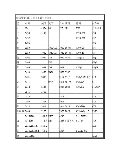
举报帖子复制贴子加为精华单贴屏蔽帖子评价变形铝及铝合金牌号对照表中国(GB) 国际(ISO)美国(AA)日本(JIS)原苏联(ΓOCT)德国(DIN)英国(BS)法国(NF)LG5 - 1199 1N99 AB000 Al99.98R S1 -LG2 - 1090 1N90 AB1 Al99.9 - -LG1 Al99.8 1080 A1080 AB2 Al99.8 1A -L1 Al99.7 1070 A1070 A00 Al99.7 - 1070A L2 - 1060 A1060 A0 - - -L3 Al99.5 1050 - A1 Al99.5 1B 1050A L5-1 Al99.0 1100 A1100 A2 Al99.0 3L54 1100 L5 - 1200 A1200 - Al99 1C 1200 LF2 AlMg2.5 5052 A5052 AMr AlMg2.5 N4 5052 LF3 AlMg3 5154 A5154 AMr3 AlMg3 N5 -LF4 AlMg4.5Mn0.7 5038 A5038 AMr4 AlMg4.5Mn N8 5083 LF5-1 AlMg5 5056 A5056 - AlMg5 N6 -LF5 AlMg5Mn0.4 5456 - Amr5 - N61 -LF21 AlMn1Cu 3003 A3003 AMu AlMnCu N3 3003 LD2 - 6165 A6165 AB - - -LD7 AlCu2MgNi 2618 2N01 AK4 - H16 2618A LD9 - 2018 A2018 AK2 - - -LD10 AlCu4SiMg 2014 A2014 AK8 AlCuSiMg - 2014 LD11 - 4032 A4032 AK9 - 38S 4032LD30 AlMg1SiCu 6061 A6061 AΠ33AlMg1SiCu H20 6061 LD31 AlMg0.7Si 6063 A6063 AΠ31AlMgSi0.5 H19 -LY1 AlCu2.5Mg 2217 A2217 AΠ18AlCu2.5Mg0.5 3L86 -LY11 AlCu4MgSi 2017 A2017 AΠ1AlCuMg1 H15 2017A LY12 AlCu4Mg1 2024 A2024 AΠ16AlCuMg2 GB-24S 2024 LC3 AlZn7MgCu 7174 - B94 - - -LC9 AlZn5.5MgCu 7075 A7075 - AlZnMgCu1.5 L95 7075 LC10 - 7079 7N11 - AlZnMgCu0.5 - -LT1 AlSi5 4043 A4043 AK AlSi5 N21 -LT17 AlSi12 4047 A4047 - AlSi12 N2 -LB1 - 7072 A7072 - SlZn1 - -举报帖子删除单贴复制贴子加为精华单贴屏蔽帖子评价中国新旧合金牌号对照表(GB/T 3190-1996)新牌号旧牌号新牌号旧牌号新牌号旧牌号1A99 原LG5 2B12 原LY9 3003 -举报帖子删除单贴复制贴子加为精华单贴屏蔽帖子评价铝合金的特性与用途——李伟类别:防锈铝牌号: LF21 是应用最广的一种防锈铝,它的强度不高,不能热处理强化,在退火状态下有高的塑性,而蚀性好,焊接性好,切削加工性不良。
5082-G513-K0300中文资料

DevicesAlGaAs Orange Red HER Green Package HDSP-HDSP-HDSP-HDSP- DescriptionDrawingA411A111A211A5117.6 mm Common Anode Right Hand Decimal A A413A113A213A5137.6 mm Common Cathode Right Hand Decimal B F411F111F211F51110 mm Common Anode Right Hand Decimal C F413F113F213F51310 mm Common Cathode Right Hand Decimal D G411G111G211G51110 mm Two Digit Common Anode Right Hand Decimal E G413G113G213G51310 mm Two Digit Common Cathode Right Hand Decimal F H411H111H211H51114.2 mm Common Anode Right Hand Decimal G H413H113H213H51314.2 mm Common Cathode Right Hand Decimal H K411K111K211K51114.2 mm Two Digit Common Anode Right Hand Decimal I K413K113K213K51314.2 mm Two Digit Common Cathode Right Hand DecimalJBlack Surface Seven Segment Displays Technical DataFeatures• Black Surface and Color Tinted Epoxy• Industry Standard Size • Industry Standard Pinout • Choice of Character Size 7.6 mm (0.30 in.), 10 mm (0.40in.), 14.2 mm (0.56 in.)• Choice of ColorsAlGaAs Red, High Efficiency Red (HER), Green, Orange • Excellent Appearance Evenly Lighted Segments ±50° Viewing Angle• Design FlexibilityCommon Anode or Common CathodeSingle and Two Digit• Categorized for Luminous IntensityCategorized for Color: Green Use of Like Categories Yields a Uniform Display• Excellent for Long Digit String MultiplexingDescriptionThese devices use industrystandard size package and pinout.Available with black surfaceHDSP-AX11/-AX13 Series HDSP-FX11/-FX13 Series HDSP-GX11/-GX13 Series HDSP-HX11/-HX13 Series HDSP-KX11/-KX13 Seriesfinish. All devices are available as either common anode or common cathode.Typical applications includeappliances, channel indicators of TV, CATV converters, game machines, and point of sale terminals.Part Numbering System5082 -X X X X-X X X X XHDSP-X X X X-X X X X XMechanical Options[1]00: No Mechanical OptionColor Bin Options[1,2]0: No Color Bin LimitationMaximum Intensity Bin[1,2]0: No Maximum Intensity Bin LimitationMinimum Intensity Bin[1,2]0: No Minimum Intensity Bin LimitationDevice Configuration/Color[1]1: Common Anode3: Common CathodeDevice Specific Configuration[1]Refer to Respective DatasheetPackage[1]A: 7.6 mm (0.3 inch) Single Digit Seven Segment DisplayF: 10 mm (0.4 inch) Single Digit Seven Segment DisplayG: 10 mm (0.4 inch) Dual Digit Seven Segment DisplayH: 14.2 mm (0.56 inch) Single Digit Seven Segment DisplayK: 14.2 mm (0.56 inch) Dual Digit Seven Segment Display Notes:1. For codes not listed in the figure above, please refer to the respective datasheet or contact your nearestAgilent representative for details.2. Bin options refer to shippable bins for a part number. Color and Intensity Bins are typically restricted to 1bin per tube (exceptions may apply). Please refer to respective datasheet for specific bin limit information.Package Dimensions (7.6 mm Series)Internal Circuit DiagramPackage Dimensions (10 mm Series: Single)Internal Circuit DiagramPackage Dimensions (10 mm Series: Two Digit)Internal Circuit DiagramPackage Dimensions (14.2 mm Series: Single)Internal Circuit DiagramPackage Dimensions (14.2 mm Series: Two Digit)Internal Circuit Diagram2DIGIT NO. 1 CATHODE1Absolute Maximum RatingsAlGaAs Red HER/Orange GreenHDSP-X11X HDSP-X21X/X41X HDSP-X51X Description Series Series Series Units Average Power per Segment37105105mW or DPPeak Forward Current per4590[1]90[3]mA Segment or DPDC Forward Current per15[5]30[2]30[4]mA Segment or DPOperating Temperature Range–20 to +100 –40 to +100°C Storage Temperature Range–55 to +100°C Reverse Voltage per 3.0V Segment or DPWave Soldering Temperature for250°C 3 Seconds (1.60 mm [0.063 in.]below Body)Notes:1. See Figure 5 to establish pulsed conditions.2. Derate above 53°C at 0.45 mA/°C (see Figure 7).3. See Figure 6 to establish pulsed conditions.4. Derate above 39°C at 0.37 mA/°C (see Figure 7).5. Derate above 91°C at 0.53 mA/°C (see Figure 1).Electrical/Optical Characteristics at T A = 25°CAlGaAs RedDevice SeriesHDSP-Parameter Symbol Min.Typ.Max.Units Test Conditions A11X Luminous Intensity/Segment[1,2]I V315600µcd I F = 1 mA (Digit Average)3600I F = 5 mAF11X, G11X330650I F = 1 mA3900I F = 5 mAH11X, K11X400700I F = 1 mA4200I F = 5 mAAll Devices Forward Voltage/Segment or DP V F 1.6 2.0V I F = 1 mA1.7I F = 5 mA1.822I F = 20 mA PeakPeak WavelengthλP EAK645nmDominant Wavelength[3]λd637nmReverse Voltage/Segment or DP[4]V R 3.015V I R = 100 µATemperature Coefficient of∆V F/°C-2mV/°CV F/Segment or DPA11X Thermal Resistance LED RθJ-PIN255°C/W/Junction-to-Pin Seg.F11X, G11X320H11X, K12X400OrangeDevice SeriesHDSP-Parameter Symbol Min.Typ.Max.Units Test Conditions A41X Luminous Intensity/Segment I V0.70mcd I F = 5 mA (Segment Average)[1,2]F41X, G41X 1.0I F = 5 mAH41X, K41X 2.37I F = 10 mAAll Forward Voltage/Segment or DP V F 2.0 2.5V I F = 20 mA DevicesPeak WavelengthλPEAK600nmDominant Wavelength[3]λd603nmReverse Voltage/Segment or DP[4]V R 3.030V I R = 100 µATemperature Coefficient of∆V F/°C–2mV/°CV F/Segment or DPA41X Thermal Resistance LED RθJ-PIN200°C/W/Junction-to-Pin Seg.F41X, G41X320H41X, K41X345High Efficiency RedDevice SeriesHDSP-Parameter Symbol Min.Typ.Max.Units Test Conditions A21X Luminous Intensity/Segment[1,2]I V360980µcd I F = 5 mA (Digit Average)5390I F = 20 mAF21X, G21X4201200I F = 5 mAH21X, K21X9002800I F = 10 mA3700I F = 60 mA Peak:1/6 Duty Factor All Forward Voltage/Segment or DP V F 2.0 2.5V I F = 20 mA DevicesPeak WavelengthλPEAK635nmDominant Wavelength[3]λd626nmReverse Voltage/Segment or DP[4]V R 3.030V I R = 100 µATemperature Coefficient of∆V F/°C-2mV/°CV F/Segment or DPA21X Thermal Resistance LED RθJ-PIN200°C/W/Junction-to-Pin Seg.F21X, G21X320H21X, K21X345High Performance GreenDevice SeriesHDSP-Parameter Symbol Min.Typ.Max.Units Test ConditionsA51X Luminous Intensity/Segment[1,2]I V8603000µcd I F = 10 mA (Digit Average)6800I F = 20 mAF51X, G51X10303500I F = 10 mAH51X, K51X9002500I F = 10 mA3100I F = 60 mA Peak:1/6 Duty FactorAll Forward Voltage/Segment or DP V F 2.1 2.5V I F = 10 mADevicesPeak WavelengthλPEAK566nmDominant Wavelength[3,5]λd571577nmReverse Voltage/Segment or DP[4]V R 3.050V I R = 100 µATemperature Coefficient of∆V F/°C-2mV/°CV F/Segment or DPA51X Thermal Resistance LED RθJ-PIN200°C/W/Junction-to-Pin Seg.F51X, G51X320H51X, G51X345Notes:1. Case temperature of device immediately prior to the intensity measurement is 25°C.2. The digits are categorized for luminous intensity. The intensity category is designated by a letter on the side of the package.3. The dominant wavelength, λd, is derived from the CIE chromaticity diagram and is that single wavelength which defines the color ofthe device.4. Typical specification for reference only. Do not exceed absolute maximum ratings.5. Green (HDSP-A51X/F51X/G51X/H512X/K51X) series displays are categorized for dominant wavelength. The category is designated bya number adjacent to the luminous intensity category letter.Figure 3. Relative Luminous Intensity vs. DC Forward Current.Figure 4. Relative Efficiency (LuminousIntensity per Unit Current) vs. Peak Current.Figure 1. Maximum Allowable Average orDC Current vs. Ambient Temperature.Figure 2. Forward Current vs. Forward Voltage.16024681012142010090807060504030T – AMBIENT TEMPERATURE – °C AI A V E . M A X – M A X I M U M A V E R A G E F O R W A R D C U R R E N T P E R S E G M E N T – m AF 1201102018F 50.020.010.05.02.01.00.50.10.51.01.52.02.5V – FORWARD VOLTAGE – VF I – F O R W A R D C U R R E N TP E R S E G M E N T – m A20105210.50.20.10.10.20.51251020R E L A T I V E L U M I N O U S I N T E N S I T Y (N O R M A L I Z E D T O 1 A T 1 m A )I – FORWARD CURRENT PER SEGMENT – mAF I – PEAK FORWARD CURRENTPER SEGMENT – mAPEAK η –R E L A T I V E E F F I C I E N C Y – N O R M A L I Z E D T O 1 A T 1 m AP E A K 1.31.21.11.00.90.80.7AlGaAs RedHER, Green, OrangeFigure 7. Maximum Allowable DCCurrent vs. Ambient Temperature.Figure 8. Forward Current vs.Forward Voltage Characteristics.Figure 9. Relative Luminous Intensity vs. DC Forward Current.Figure 10. Relative Efficiency (Luminous Intensity per Unit Current) vs. Peak Current.40051015202530352010090807060504030T – AMBIENT TEMPERATURE – °CA I M A X – M A X I M U M D C C U R R E N T P E R S E G M E N T – m AD C 1201105045010080604020I – F O R W A R D C U R R E N T P E R S E G M E N T – m AF 2.04.03.01.0V –FORWARD VOLTAGE – VF 05.0ηP E A K – R E L A T I V E L U M I N O U S I N T E N S I T Y (N O R M A L I Z E D T O 1 A T 5 m A F O R H E R ,A N D T O 1 A T 10 m A F O R G R E E N )150108642205301025I – FORWARD CURRENT PER SEGMENT – mAF 0I – PEAK FORWARD CURRENTPER SEGMENT – mAPEAK ηP E A K – R E L A T I V E E F F I C I E N C Y (N O R M A L I Z E D T O 1 A T 5 m A F O R H E R ,A N D 10 m A F O R G R E E N )Figure 5. Maximum Tolerable Peak Currentvs. Pulse Duration – HER, Orange.Figure 6. Maximum Tolerable Peak Current vs. Pulse Duration – Green.R A T I O O F M A X I M U M O P E R A T I N G P E A K C U R R E N T T O T E M P E R A T U R E D E R A T E D D C C U R R E N TI P E A K F I M A X D C t – PULSE DURATION – µsP 101100DC R A T I O O F M A X I M U M O P E R A T I N G P E A K C U R R E N T T O T E M P E R A T U R E D E R A T E D D C C U R R E N TI P E A K FI M A X D C t – PULSE DURATION – µs P 101100DCHDSP-A1xx IV Bin Category Min.Max.E 0.3150.520F 0.4280.759G 0.621 1.16H 0.945 1.71I 1.40 2.56J 2.10 3.84K 3.14 5.75L 4.708.55Intensity Bin Limits (mcd)AlGaAs RedHDSP-F1xx/G1xx IV Bin Category Min.Max.D 0.3910.650E 0.5320.923F 0.755 1.39G 1.13 2.08H 1.703.14HDSP-H1xx/K1xx IV Bin Category Min.Max.C 0.4150.690D 0.5650.990E 0.810 1.50F 1.20 2.20G 1.80 3.30H 2.73 5.00I 4.097.50OrangeHDSP-A41XIV Bin Category MinMaxA 0.2840.433B 0.3540.541C 0.4430.677D 0.5540.846E 0.692 1.057F 0.856 1.322G 1.082 1.652H 1.352 2.066I 1.692 2.581J 2.114 3.227K 2.641 4.034L 3.300 5.042M 4.127 6.303N 5.1577.878HDSP-F41X/G41XIV Bin Category MinMaxC 0.4850.890D 0.728 1.333E 1.091 2.000F 1.636 3.000G 2.454 4.500H 3.6826.751HDSP-H41X/K41XIV Bin Category MinMaxB 0.77 1.17C 0.95 1.45D 1.19 1.82E 1.49 2.27F 1.85 2.89G 2.32 3.54H 2.904.43Intensity Bin Limits (mcd), continued HERMin.Max.B0.3420.630C0.5160.946D0.774 1.418E 1.160 2.127F 1.740 3.190G 2.610 4.785H 3.9157.177Min.Max.C0.4850.890D0.728 1.333E 1.091 2.000F 1.636 3.000G 2.454 4.500H 3.682 6.751Min.Max.E0.91 1.67F 1.37 2.51G 2.05 3.76H 3.08 5.64I 4.628.64J 6.9312.70K10.3919.04Contrast EnhancementFor information on contrast enhancement, please see Application Note 1015.Soldering/CleaningFor information on soldering LEDs, please refer to Application Note 1029.Electrical/OpticalFor more information onelectrical/optical characteristics,please see Application Note 1005.Color CategoriesNote:All categories are established for classification of products. Products may not be available in all categories. Please contact your Agilent representatives for further clarification/information.HDSP-A5xx IV Bin Category Min.Max.H 0.86 1.58I 1.29 2.37J 1.94 3.55K 2.90 5.33L 4.378.01Intensity Bin Limits (mcd), continued GreenHDSP-F5xx/G5xx IV Bin Category Min.Max.H 1.54 2.82I 2.31 4.23J 3.46 6.34K 5.189.50L 7.7814.26HDSP-H5xx/K5xx IV Bin Category Min.Max.E 0.91 1.67F 1.37 2.51G 2.05 3.76H 3.08 5.64I 4.618.46/semiconductors For product information and a complete list of distributors, please go to our web site.For technical assistance call:Americas/Canada: +1 (800) 235-0312 or (916) 788-6763Europe: +49 (0) 6441 92460China: 10800 650 0017Hong Kong: (+65) 6756 2394India, Australia, New Zealand: (+65) 6755 1939 Japan: (+81 3) 3335-8152 (Domestic/Interna-tional), or 0120-61-1280 (Domestic Only) Korea: (+65) 6755 1989Singapore, Malaysia, Vietnam, Thailand, Philippines, Indonesia: (+65) 6755 2044 Taiwan: (+65) 6755 1843Data subject to change.Copyright © 2004 Agilent Technologies, Inc. Obsoletes 5988-1742ENJuly 17, 20045988-4433EN。
5082-7403-FFZ00资料

7.6 mm (0.3 inch) Micro Bright Seven Segment Displays Technical DataFeatures• Available with Colon for Clock Display • Compact Package 0.300 x 0.500 inchesLeads on 2.54 mm (0.1 inch)Centers• Choice of Colors AlGaAs Red, HighEfficiency Red, Yellow, Green,Orange• Excellent Appearance Evenly Lighted Segments Mitered Corners on Segments Surface Color Gives Optimum Contrast±50° Viewing Angle • Design FlexibilityCommon Anode or Common CathodeRight Hand Decimal Point ±1. Overflow Character • Categorized for Luminous IntensityYellow and Green Categorized for ColorUse of Like Categories Yields a Uniform Display • High Light Output • High Peak Current• Excellent for Long Digit String Multiplexing • Intensity and Color Selection Available See Intensity and ColorSelected Displays Data Sheet • Sunlight Viewable AlGaAsDescriptionThe 7.6 mm (0.3 inch) LED seven segment displays are designed for viewing distances up to 3 metres (10 feet). These devices use an industry standard size package and pinout. Both the numeric andDevicesOrange AlGaAs [1]HER [1]Yellow [1]Green [1]Package HDSP-HDSP-HDSP-HDSP-HDSP- DescriptionDrawingA401A151750174017801Common Anode Right A Hand Decimal750274027802Common Anode Right Hand B Decimal, Colon A403A153750374037803Common Cathode Right C Hand Decimal750474047804Common Cathode Right Hand D Decimal, ColonA157750774077807Common Anode ±1. Overflow E A158750874087808Common Cathode ±1. OverflowFNote:1. These displays are recommended for high ambient light operation. Please refer to the HDSP-A10X AlGaAs, HDSP-335X HER, HDSP-A80X Yellow, and HDSP-A90X Green data sheet for low current operation.HDSP-740x Series HDSP-750x Series HDSP-780x Series HDSP-A15x Series HDSP-A40x Series±1. overflow devices feature a right hand decimal point. All devices are available as either common anode or common cathode.These displays are ideal for most applications. Pin for pin equiv-alent displays are also available in a low current design. The low current displays are ideal forportable applications. For additional information see the Low Current Seven Segment Displays.Part Numbering SystemNotes:1. For codes not listed in the figure above, please refer to the respective datasheet or contact your nearest Agilent representative for details.2. Bin options refer to shippable bins for a part number. Color and Intensity Bins are typically restricted to 1bin per tube (exceptions may apply). Please refer to respective datasheet for specific bin limit information.5082 -X X X X-X X X X X HDSP-X X X X-X X X X XMechanical Options [1]00: No Mechanical OptionColor Bin Options [1,2]0: No Color Bin Limitation3: Color Bins 3- and 3+ only (applicable for Yellow devices only)Z: Color Bins 2- and 3+ only (applicable for Yellow devices only)Maximum Intensity Bin [1,2]0: No Maximum Intensity Bin Limitation Minimum Intensity Bin [1,2]0: No Minimum Intensity Bin Limitation Device Configuration/Color [1]1: Common Anode 2: Common Anode 3: Common Cathode 4: Common CathodeDevice Specific Configuration [1]Refer to Respective DatasheetPackage [1]A: 7.6 mm (0.3 inch) Single Digit Seven Segment DisplayPackage Dimensions NOTES:1. ALL DIMENSIONS IN MILLIMETRES (INCHES).2. MAXIMUM.3. ALL UNTOLERANCED DIMENSIONS AREFOR REFERENCE ONLY.4. REDUNDANT ANODES.5. REDUNDANT CATHODES.6. FOR HDSP-7400/-7800 SERIES PRODUCT ONLY.Device Series HDSP-ParameterSymbol Min.Typ.Max.Units Test Conditions Luminous Intensity/Segment [1,2,5]I V6.914.0mcd I F = 20 mA (Digit Average)1.8VI F = 20 mAForward Voltage/Segment or DPV F2.03.0V I F = 100 mAA15xPeak Wavelength λPEAK 645nm Dominant Wavelength [3]λd 637nm Reverse Voltage/Segment or DP [4]V R 3.015.0V I R = 100 µA Temperature Coefficient of ∆V F /°C -2mV/°C V F /Segment or DPThermal Resistance LED Junction-R θJ-PIN255°C/W/Segto-PinAlGaAs RedElectrical/Optical Characteristics at T A = 25°C Absolute Maximum RatingsAlGaAs Red HER/Orange Yellow GreenHDSP-A150HDSP-7500/-A40X HDSP-7400HDSP-7800DescriptionSeriesSeries SeriesSeriesUnits Average Power per Segment or DP 9610580105mW Peak Forward Current per 160[1]90[3]60[5]90[7]mA Segment or DPDC Forward Current per 40[2]30[4]20[6]30[8]mASegment or DPOperating Temperature Range –20 to +100[9]–40 to +100°CStorage Temperature Range –55 to +100°C Reverse Voltage per Segment or DP 3.0V Lead Solder Temperature for 3Seconds (1.59 mm [0.063 in.] 260°Cbelow seating plane)Notes:1. See Figure 1 to establish pulsed conditions.2. Derate above 46°C at 0.54 mA/°C.3. See Figure 6 to establish pulsed conditions.4. Derate above 53°C at 0.45 mA/°C.5. See Figure 7 to establish pulsed conditions.6. Derate above 81°C at 0.52 mA/°C.7. See Figure 8 to establish pulsed conditions.8. Derate above 39°C at 0.37 mA/°C.9. For operation below –20°C, contact your local Agilent components sales office or an authorized distributor.High Efficiency RedDeviceSeriesHDSP-Parameter Symbol Min.Typ.Max.Units Test Conditions Luminous Intensity/Segment[1,2,6]360980I F = 5 mA(Digit Average)I Vµcd5390I F = 20 mA Forward Voltage/Segment or DP V F 2.0 2.5V I F = 20 mA 750x Peak WavelengthλPEAK635nmDominant Wavelength[3]λd626nmReverse Voltage/Segment or DP[4]V R 3.030V I R = 100 µATemperature Coefficient of∆V F/°C-2mV/°CV F/Segment or DPThermal Resistance LED Junction-RθJ-PIN200°C/W/Segto-PinOrangeDeviceSeriesHDSP-Parameter Symbol Min.Typ.Max.Units Test Conditions Luminous Intensity/Segment[1,2,6]I V0.70mcd I F = 5 mA(Digit Average)Forward Voltage/Segment or DP V F 2.0 2.5V I F = 20 mA A40x Peak WavelengthλPEAK600nmDominant Wavelength[3]λd603nmReverse Voltage/Segment or DP[4]V R 3.030V I R = 100 µATemperature Coefficient of∆V F/°C-2mV/°CV F/Segment or DPThermal Resistance LED Junction-RθJ-PIN200°C/W/Segto-PinYellowDeviceSeriesHDSP-Parameter Symbol Min.Typ.Max.Units Test Conditions Luminous Intensity/Segment[1,2,7]225480I F = 5 mA(Digit Average)I Vµcd2740I F = 20 mA Forward Voltage/Segment or DP V F 2.2 2.5V I F = 20 mA 740x Peak WavelengthλPEAK583nmDominant Wavelength[3,9]λd581.5586592.5nmReverse Voltage/Segment or DP[4]V R 3.050.0V I R = 100 µATemperature Coefficient of∆V F/°C-2mV/°CV F/Segment or DPThermal Resistance LED Junction-RθJ-PIN200°C/W/Segto-PinHigh Performance GreenDeviceSeriesHDSP-Parameter Symbol Min.Typ.Max.Units Test Conditions Luminous Intensity/Segment[1,2,8]8603000I F = 10 mA(Digit Average)I Vµcd6800I F = 20 mA Forward Voltage/Segment or DP V F 2.1 2.5V I F = 10 mA 780x Peak WavelengthλPEAK566nmDominant Wavelength[3,9]λd571577nmReverse Voltage/Segment or DP[4]V R 3.050.0V I R = 100 µATemperature Coefficient of∆V F/°C-2mV/°CV F/Segment or DPThermal Resistance LED Junction-RθJ-PIN200°C/W/Segto-PinNotes:1. Case temperature of device immediately prior to the intensity measurement is 25°C.2. The digits are categorized for luminous intensity. The intensity category is designated by a letter on the side of the package.3. The dominant wavelength, λd, is derived from the CIE chromaticity diagram and is that single wavelength which defines the color ofthe device.4. Typical specification for reference only. Do not exceed absolute maximum ratings.5. For low current operation the AlGaAs HDSP-A101 series displays are recommended.6. For low current operation the HER HDSP-7511 series displays are recommended.7. For low current operation the Yellow HDSP-A801 series displays are recommended.8. For low current operation the Green HDSP-A901 series displays are recommended.9. The yellow (HDSP-7400) and Green (HDSP-7800) displays are categorized for dominant wavelength. The category is designated by anumber adjacent to the luminous intensity category letter.AlGaAs Redt – PULSE DURATION – µs P101100R A T I O O F M A X I M U M O P E R A T I N G P E A K C U R R E N T T O T E M P E R A T U R E D E R A T E D M A X I M U M D C C U R R E N TI P E A K F I M A X DC Figure 4. Relative Luminous Intensity vs. DC Forward Current.Figure 2. Maximum Allowable DC Current per Segment as a Function of Ambient Temperature.Figure 1. Maximum Allowed Peak Current vs.Pulse Duration – AlGaAs Red.Figure 5. Relative Efficiency (LuminousIntensity per Unit Current) vs. Peak Current.Figure 3. Forward Current vs.Forward Voltage.T A – AMBIENT TEMPERATURE – °C I D C M A X . – M A X I M U M D C C U R R E N T P E R S E G M E N T– m AV F – FORWARD CURRENT – VI F – F O R W A R D C U R R E N T P E R S E G M E N T – m AI PEAK – PEAK FORWARD CURRENT PER SEGMENT – mAηP E A K – N O R M A L I Z E D R E L A T I V E E F F I C I E N C YI F – FORWARD CURRENT PER SEGMENT – mA R E L A T I V E L U M I N O U S I N T E N S I T Y (N O R M A L I Z E D T O 1 A T 20 m A )Figure 12. Relative Efficiency (Luminous Intensity per Unit Current) vs. Peak Current.ηP E A K – R E L A T I V E E F F I C I E N C Y (N O R M A L I Z E D T O 1 A T 5 m A F O R H E R ,O R A N G E A N D Y E L L O W , A N D 10 m A F O R G R E E N )I PEAK – PEAK FORWARD CURRENTPER SEGMENT – mAHER, Yellow, Green, OrangeFigure 6. Maximum Tolerable Peak Current vs.Pulse Duration – HER, Orange.Figure 7. Maximum Tolerable Peak Current vs. Pulse Duration – Yellow.Figure 10. Forward Current vs.Forward Voltage Characteristics.Figure 11. Relative LuminousIntensity vs. DC Forward Current.Figure 8. Allowable Peak Current vs.Pulse Duration – Green.Figure 9. Maximum Allowable DC Current per Segment as a Function of Ambient Temperature.R A T I O O F M A X I M U M O P E R A T I N G P E A K C U R R E N T T O T E M P E R A T U R E D E R A T E D D C C U R R E N TI P E A K F I M A X D C t – PULSE DURATION – µs P 101100DCR A T I O O F M A X I M U M O P E R A T I N G P E A K C U R R E N T T O T E M P E R A T U R E D E R A T E D D C C U R R E N TI P E A K FI M A X D C t – PULSE DURATION – µs P101100R A T I O O F M A X I M U M O P E R A T I N G P E A K C U R R E N T T O T E M P E R A T U R E D E R A T E D D C C U R R E N TI P E A K FI M A X D C t – PULSE DURATION – µs P10110040051015202530352010090807060504030T – AMBIENT TEMPERATURE – °C AI M A X –M A X I M U M D C C U R R E N T P E R S E G M E N T – m AD C120110504510080604020I – F O R W A R D C U R R E N T P E R S E G M E N T – m A FV – FORWARD VOLTAGE – V F R E L A T I V E L U M I N O U S I N T E N S I T Y (N O R M A L I Z E D T O 1 A T 5 m A F O R H E R A N D )t (Y E L L O W A N D T O1 A T 10 m A F O R G R E E N )1510205301025I – FORWARD CURRENT PER SEGMENT – mA FHDSP-A15x IV Bin Category Min.Max.M 7.0713.00N 10.6019.40O 15.9029.20P 23.9043.80Q 35.8065.60Intensity Bin Limits (mcd)AlGaAs RedHDSP-750x IV Bin Category Min.Max.B 0.3420.630C 0.5160.946D 0.774 1.418E 1.160 2.127F 1.740 3.190G 2.610 4.785H 3.9157.177HERHDSP-740x IV Bin Category Min.Max.B 0.2290.387C 0.3170.582D 0.4760.872E 0.714 1.311F 1.073 1.967G 1.609 2.950H 2.4134.425YellowHDSP-780x IV Bin Category Min.Max.H 0.86 1.58I 1.29 2.37J 1.94 3.55K 2.90 5.33L 4.378.01GreenOrangeHDSP-A40XIV Bin Category Min.Max.A 0.2840.433B 0.3540.541C 0.4430.677D 0.5540.846E 0.692 1.057F 0.856 1.322G 1.082 1.652H 1.352 2.066I 1.692 2.581J 2.114 3.227K 2.641 4.034L 3.300 5.042M 4.127 6.303N 5.1577.878Color CategoriesNote:All categories are established for classification of products. Products may not be available in all categories. Please contact your Agilent representatives for further clarification/information.Contrast EnhancementFor information on contrastenhancement, please seeApplication Note 1015.Soldering/CleaningCleaning agents from the ketonefamily (acetone, methyl ethylketone, etc.) and from thechlorinated hydrocarbon family(methylene chloride, trichloro-ethylene, carbon tetrachloride,etc.) are not recommended forcleaning LED parts. All of thesevarious solvents attack or dissolvethe encapsulating epoxies used toform the package of plastic LEDparts.For further information onsoldering LEDs, please refer toApplication Note 1027.元器件交易网/semiconductorsFor product information and a complete list ofdistributors, please go to our web site.For technical assistance call:Americas/Canada: +1 (800) 235-0312 or(408) 654-8675Europe: +49 (0) 6441 92460China: 10800 650 0017Hong Kong: (+65) 271 2451India, Australia, New Zealand: (+65) 271 2394Japan: (+81 3) 3335-8152(Domestic/Interna-tional), or 0120-61-1280(Domestic Only)Korea: (+65) 271 2194Malaysia, Singapore: (+65) 271 2054Taiwan: (+65) 271 2654Data subject to change.Copyright © 2002 Agilent Technologies, Inc.Obsoletes 5988-0382ENFebruary 11, 20025988-4434EN。
508中文说明书

MAXBOND 508 进一步提高了以前产品的电性能和热阻,它是一种由氯丁二烯组成的符合UL 94-O标准的高阻燃级别胶水. 它是一种在常温下粘接的胶水,只要施加小小的压制它就会表现出很强的粘接力1. 规格主要成分:合成树脂颜色:白色粘性液体固体含量: 63 ~ 67粘度(25℃): 45,000 ~ 65,000 CPS比重: 1.30 ± 0.05闪点: - 7 ℃燃点: 515 ℃工作温度:100℃~120℃贮藏期: 9 个月表面干燥时间:1mm厚 3分钟(20~25℃)2. 特征适用于电子电气零件的固定、绝缘、密封和安装1) 可用于铜、铝、铁等金属的粘接2) 可用于丙烯腈、苯乙烯、树脂类硬质塑料的粘接3) 它具有良好的可使用性,拉丝现象少,不松垂,可用于各种粘接3. 应用1) 用于密封、粘接和固定,起到绝缘、挡灰、振动试验和固定电子电器部件的作用2) 将零散部件固定在印制电路板上3) 在焊接过程中将大部件固定阻止其移动4) 一般用于粘接金属、玻璃、塑料、橡胶、木料等材质4. 胶水在用胶后10天内的特征* 开始 = 在60℃条件下固化后3小时* 切变强度= PVC / PVC* 剥离强度= PVC / PVC5.不同温度下的剥离强度* 在100℃条件下3小时固化后测量6. 胶水在不同固化过程下的切力强度7.胶水在-40℃ 1H固化后测定的切变强度* (-40℃) 是在空气温度为-40℃8.松垂15mm 或以下情况* 将25mmφ× 3.5mm 厚的胶水试剂涂在2mm厚的铝板上,然后立即将板垂直放置。
一分钟以后,再测定胶水的流动。
9.电气特性1) 注意空气流通和防火2) 储藏必须通风3) 用甲苯和稀释剂清洗。
5082-2800中文资料

Schottky Barrier Diodes for General Purpose ApplicationsTechnical DataFeatures• Low Turn-On VoltageAs Low as 0.34 V at 1 mA• Pico Second Switching Speed • High Breakdown VoltageUp to 70 V• Matched Characteristics AvailableDescription/Applications The 1N5711, 1N5712, 5082-2800/ 10/11 are passivated Schottky barrier diodes which use a patented “guard ring” design to achieve a high breakdown voltage. Packaged in a low cost glass package, they are well suited for high level detecting, mixing, switching, gating, log or A-D converting, video detecting, frequency discriminating, sampling, and wave shaping.The 5082-2835 is a passivatedSchottky diode in a low cost glasspackage. It is optimized for lowturn-on voltage. The 5082-2835 isparticularly well suited for theUHF mixing needs of the CATVmarketplace.The 5082-2300 Series and5082-2900 devices are unpas-sivated Schottky diodes in a glasspackage. These diodes haveextremely low 1/f noise and areideal for low noise mixing, andhigh sensitivity detecting. Theyare particularly well suited for usein Doppler or narrow band videoreceivers.1N57111N57125082-2300 Series5082-2800 Series5082-2900DIMENSIONS IN MILLIMETERS AND (INCHES).Outline 15Maximum RatingsJunction Operating and Storage Temperature Range5082-2303, -2900.................................................................-60°C to +100°C 1N5711, 1N5712, 5082-2800/10/11....................................-65°C to +200°C 5082-2835............................................................................-60°C to +150°C DC Power Dissipation(Measured in an infinite heat sink at T CASE = 25°C)Derate linearly to zero at maximum rated temperature5082-2303, -2900..............................................................................100 mW 1N5711, 1N5712, 5082-2800/10/11.................................................250 mW 5082-2835.........................................................................................150 mW Peak Inverse Voltage.................................................................................V BRPackage CharacteristicsOutline 15Lead Material........................................................................................DumetLead Finish..............................................................................95-5% Tin-LeadMax. Soldering Temperature................................................260°C for 5 secMin. Lead Strength....................................................................4 pounds pullTypical Package Inductance1N5711, 1N5712:................................................................................2.0 nH2800 Series:........................................................................................2.0 nH2300 Series, 2900:..............................................................................3.0 nHTypical Package Capacitance1N5711, 1N5712:................................................................................0.2 pF2800 Series:........................................................................................0.2 pF2300 Series, 2900:............................................................................0.07 pFThe leads on the Outline 15 package should be restricted so that thebend starts at least 1/16 inch from the glass body.Outline 15 diodes are available on tape and reel. The tape and reelspecification is patterned after RS-296-D.Electrical Specifications at T= 25°CAGeneral Purpose DiodesMin.Max.V F = 1 V Max.Max.Max.Breakdown Forward at Forward Reverse Leakage Capaci-Part Package Voltage Voltage Current Current tance Number Outline V BR (V)V F (mV)I F (mA)I R (nA) at V R (V)C T (pF) 5082-280015704101520050 2.0 1N571115704101520050 2.0 5082-281015204103510015 1.2 1N571215205503515016 1.2 5082-28111515410201008 1.2 5082-2835158*34010*1001 1.0 Test I R = 10 µA I F = 1 mA*V F = 0.45 V V R = 0 V Conditions*I R = 100 µA f =1.0 MHz Note: Effective Carrier Lifetime (τ) for all these diodes is 100 ps maximum measured with Krakauer method at 5 mA except for 5082-2835 which is measured at 20 mA.Low 1/f (Flicker) Noise DiodesMin.Max.V F = 1 V Max.Max.Max.Part Breakdown Forward at Forward Reverse Leakage Capaci-Number Package Voltage Voltage Current Current tance 5082-Outline V BR (V)V F (mV)I F (mA)I R (nA) at V R (V)C T (pF) 230315204003550015 1.0 29001510400201005 1.2 Test I R = 10 µA I F = 1 mA V R = 0 V Conditions f =1.0 MHzNote: Effective Carrier Lifetime (τ) for all these diodes is 100 ps maximum measured with Krakauer method at 20 mA.Matched Pairs and QuadsBasic Matched MatchedPart Number Pair Quad Batch5082-Unconnected Unconnected Matched[1]Test Conditions2900∆VF at IF= 1.0, 10 mA28005082-28045082-2805∆V F at I F = 0.5, 5 mA ∆V F = 20 mV∆V F = 20 mV*I F = 10 mA∆C O at f = 1.0 MHz28115082-2826∆VF at IF= 10 mA∆V F = 10 mV∆C O at f = 1.0 MHz ∆C O = 0.1 pF28355082-2080∆VF at IF=10 mA∆V F = 10 mV∆C O at f = 1.0 MHz∆C O = 0.1 pFNote:1. Batch matched devices have a minimum batch size of 50 devices.SPICE ParametersParameter Units5082-28005082-28105082-28115082-28355082-23035082-2900B V V75251892510C J0pF 1.60.8 1.00.70.7 1.1E G eV0.690.690.690.690.690.69I BV A10E-510E-510E-510E-510E-510E-5I S A 2.2 x 10E-9 1.1 x 10E-90.3 x 10E-8 2.2 x 10E-87 x 1.0E-910E-8N 1.08 1.08 1.08 1.08 1.08 1.08 R SΩ25101051015 P B V0.60.60.60.560.640.64 PT222222 M0.50.50.50.50.50.5Typical ParametersV F – FORWARD VOLTAGE (V)Figure 1. I-V Curve Showing Typical Temperature Variation for 5082-2300 Series and 5082-2900 Schottky Diodes.1001010.10.01I F - F O R W A R D C U R R E N T (m A )V BR (V)Figure 2. 5082-2300 Series Typical Reverse Current vs. Reverse Voltage at Various Temperatures.10.0001,000100101I R (n A )051015100755025T A = 25°CI F - FORWARD CURRENT (mA)Figure 3. 5082-2300 Series and 5082-2900 Typical Dynamic Resistance (R D ) vs. Forward Current (I F ).100010010R D - D Y N A M I C R E S I S T AN C E (Ω)0.01010100V R - REVERSE VOLTAGE (V)Figure 4. 5082-2300 and 5082-2900 Typical Capacitance vs. Reverse Voltage.1.21.00.80.60.40.20C T - C A P A C I T A N C E (p F )048121620V F - FORWARD VOLTAGE (V)Figure 5. I-V Curve Showing Typical Temperature Variation for 5082-2800 or 1N5711 Schottky Diodes.5010510.50.10.050.01I F - F O R W A R D C U R R E N T (m A )00.20.40.60.8 1.0 1.2V R - REVERSE VOLTAGE (V)Figure 6. (5082-2800 OR 1N5711) Typical Variation of Reverse Current (I R ) vs. Reverse Voltage (V R ) at Various Temperatures.100,00010,0001000100101I R - R E V E R S E C U R R E N T (n A )0.20.40.60.81.01.2V R - REVERSE VOLTAGE (V)Figure 7. (5082-2800 or 1N5711)Typical Capacitance (C T ) vs. Reverse Voltage (V R ).12.01.51.00.50C T - C A P A C I T A N C E (p F )010********V F - FORWARD VOLTAGE (V)Figure 8. I-V Curve Showing Typical Temperature Variation for the 5082-2810 or 1N5712 Schottky Diode.100101.00.10.01I F - F O R W A R D C U R R E N T (m A )V R - REVERSE VOLTAGE (V)Figure 9. (5082-2810 or IN5712)Typical Variation of Reverse Current (I R ) vs. Reverse Voltage (V R ) at Various Temperatures.10,0001000100101.0I R - R E V E R S E C U R R E N T (n A )Typical Parameters, continuedV F - FORWARD VOLTAGE (V)Figure 10. I-V Curve Showing Typical Temperature Variation for the 5082-2811 Schottky Diode.100101.00.10.01I F - F O R W A R D C U R R E N T (m A )0.40.20.60.81.01.2V R - REVERSE VOLTAGE (V)Figure 11. (5082-2811) Typical Variation of Reverse Current (I R ) vs. Reverse Voltage (V R ) at Various Temperatures.100,00010,0001000100101I R - R E V E R S E C U R R E N T (n A )0510********V F - FORWARD VOLTAGE (V)Figure 12. I-V Curve Showing Typical Temperature Variations for 5082-2835 Schottky Diode.100101.00.10.01I F - F O R W A R D C U R R E N T (m A )00.20.40.60.8 1.0 1.2V R - REVERSE VOLTAGE (V)Figure 13. (5082-2835) Typical Variation of Reverse Current (I R ) vs. Reverse Voltage (V R ) at Various Temperatures.100,00010,0001000100101I R - R E V E R S E C U R R E N T (n A )0123456V R - REVERSE VOLTAGE (V)Figure 14. Typical Capacitance (C T ) vs. Reverse Voltage (V R ).C T - C A P A C I T A N C E (p F )0246810I F - FORWARD CURRENT (mA)Figure 15. Typical Dynamic Resistance (R D ) vs. Forward Current (I F ).1000100101R D - D Y N A M I C R E S I S T A N C E (Ω)Diode Package Marking1N5xxx5082-xxxxwould be marked:1Nx xxxxx xxYWW YWWwhere xxxx are the last four digits of the 1Nxxxx or the 5082-xxxx partnumber. Y is the last digit of the calendar year. WW is the work week ofmanufacture.Examples of diodes manufactured during workweek45 of 1999:1N57125082-3080would be marked:1N53071280945945Data subject to change.Copyright © 1999 Agilent TechnologiesObsoletes 5968-4304E5968-7181E (11/99)。
5082铝板的介绍

一、5082铝板的介绍5082属于Al-Mg-Si系合金,使用范围广泛,特别是建筑业离不开此合金,是最有前途的合金。
耐蚀性好,焊接性优良,冷加工性较好,并具有中等强度。
5083的主要合金元素为镁,具有良好的成形加工性能、抗蚀性、焊接性,中等强度,用于制造飞机油箱、油管、以及交通车辆、船舶的钣金件,仪表、街灯支架与铆钉、五金制品、电器外壳等。
AL-Mn系合金,是应用最广的一种防锈铝,这种合金的强度高,特别是具有抗疲劳强度:塑性与耐腐蚀性高,不能热处理强化,,在半冷作硬化时塑性尚好,冷作硬化时塑性低,耐腐蚀好,焊接性良好,可切削性能不良,可抛光。
用途主要用于要求高的可塑性和良好的焊接性,在液体或气体介质中工作的低载荷零件,如邮箱,汽油或润滑油导管,各种液体容器和其他用深拉制作的小负荷零件:线材用来做铆钉二、5082铝板的应用范围5082铝板常用于船舶、舰艇、车辆用材、汽车和飞机板焊接件、需严格防火的压力容器、致冷装置、电视塔、钻探设备、交通运输设备、导弹元件、装甲等。
三、5082铝板的化学成份铝 Al :余量硅 Si :0.4铜 Cu :0.1镁 Mg:4.0--4.9锌 Zn:0.25锰 Mn:0.40--0.10钛 Ti :0.15铬Cr:0.05--0.25铁 Fe: 0.4单个:0.05总计:0.15四、5082铝板的力学性能抗拉强度σb (MPa):110-136伸长率δ10 (%):≥20退火温度为:415℃。
屈服强度σs (MPa) ≥110试样毛坯尺寸所有壁厚伸长率δ5 (%) ≥12五、相关技术标准铝板带国家标准(GB/T 3880-2006),适用于铝合金板带材料的统一标准。
六、5082铝板表示方法1)加工产品的牌号美国铝业协会(AA)对变形铝及铝合金的牌号表示方法,既四位数字代号表示方法,早在1957被接纳为美国国家标准(ANSIH35.1),美国主要的铝材生产企业逐渐都采用这种牌号表示方法,以后,美国军用标准(MIL),美国汽车工程师协会(SAE),美国材料与试验协会(ASTM)等都相继采用,还在推广到其他国家。
5082-5703-KH000中文资料

14.2 mm (0.56 inch)Seven Segment Displays Technical DataFeatures• Industry Standard Size • Industry Standard Pinout 15.24 mm (0.6 in.) DIP Leads on 2.54 mm (0.1 in.) Centers • Choice of ColorsAlGaAs Red, High Efficiency Red, Yellow, Green, Orange • Excellent Appearance Evenly Lighted Segments Mitered Corners on Segments Gray Package Gives Optimum Contrast±50° Viewing Angle • Design FlexibilityCommon Anode or Common CathodeSingle and Dual Digits Right Hand Decimal Point ±1. Overflow Character• Categorized for Luminous IntensityYellow and Green Categorized for ColorUse of Like Categories Yields a Uniform Display • High Light Output • High Peak Current• Excellent for Long Digit String Multiplexing • Intensity and Color Selection OptionSee Intensity and ColorSelected Displays Data Sheet • Sunlight Viewable AlGaAsDescriptionThe 14.2 mm (0.56 inch) LED seven segment displays aredesigned for viewing distances upto 7 metres (23 feet). Thesedevices use an industry standard size package and pinout. Both the numeric and ±1 overflow devices feature a right hand decimalpoint. All devices are available as either common anode or common cathode.Orange AlGaAs Red HERYellowGreen Package HDSP-HDSP-[1]HDSP-[1]HDSP-HDSP- DescriptionDrawingH401H151550157015601Common Anode Right Hand Decimal A H403H153550357035603Common Cathode Right Hand Decimal B H157550757075607Common Anode ±1. Overflow C H158550857085608Common Cathode ±1. OverflowD K401552157215621Two Digit Common Anode Right Hand DecimalE K403552357235623Two Digit Common Cathode Right Hand DecimalFDevicesNote:1. These displays are recommended for high ambient light operation. Please refer to the HDSP-H10X/K12X AlGaAs and HDSP-555X HER data sheet for low current operation.HDSP-K40x Series HDSP-550x Series HDSP-552x Series HDSP-560x Series HDSP-562x Series HDSP-570x Series HDSP-572x Series HDSP-H15x Series HDSP-H40x SeriesThese displays are ideal for most applications. Pin for pin equivalent displays are alsoavailable in a low current design.The low current displays are idealfor portable applications. For additional information see the Low Current Seven Segment Displays data sheet.Part Numbering SystemNotes:1. For codes not listed in the figure above, please refer to the respective datasheet or contact your nearest Agilent representative for details.2. Bin options refer to shippable bins for a part number. Color and Intensity Bins are typically restricted to 1bin per tube (exceptions may apply). Please refer to respective datasheet for specific bin limit information.5082 -X X X X-X X X X X HDSP-X X X X-X X X X XMechanical Options [1]00: No Mechanical Option Color Bin Options [1,2]0: No Color Bin LimitationMaximum Intensity Bin [1,2]0: No Maximum Intensity Bin Limitation Minimum Intensity Bin [1,2]0: No Minimum Intensity Bin Limitation Device Configuration/Color [1]1: Common Anode 3: Common CathodeDevice Specific Configuration [1]Refer to Respective DatasheetPackage [1]H: 14.2 mm (0.56 inch) Single Digit Seven Segment DisplayFUNCTIONPIN AB CDEF1CATHODE e ANODE e CATHODE c ANODE cE CATHODE NO. 1 E ANODE NO. 12CATHODE d ANODE d ANODE c, d CATHODE c, d D CATHODE NO. 1 D ANODE NO. 13ANODE [3]CATHODE [4]CATHODE b ANODE bC CATHODE NO. 1 C ANODE NO. 14CATHODE c ANODE c ANODE a, b, DP CATHODE a, b, DP DP CATHODE NO. 1DP ANODE NO. 15CATHODE DP ANODE DP CATHOPDE DP ANODE DE E CATHODE NO. 1 E ANODE NO. 26CATHODE b ANODE b CATHODE a ANODE aD CATHODE NO. 2 D ANODE NO. 27CATHODE a ANODE a ANODE a, b, DP CATHODE a, b, DP G CATHODE NO. 2G ANODE NO. 28ANODE [3]CATHODE [4]ANODE c, d CATHODE c, d C CATHODE NO. 2 C ANODE NO. 29CATHODE f ANODE f CATHODE d ANODE d DP CATHODE NO. 2DP ANODE NO. 210CATHODE g ANODE g NO PINNO PINB CATHODE NO. 2 B ANODE NO. 211 A CATHODE NO. 2 A ANODE NO. 212 F CATHODE NO. 2 F ANODE NO. 213DIGIT NO. 2 ANODE DIGIT NO. 2 CATHODE 14DIGIT NO. 1 ANODE DIGIT NO. 1 CATHODE 15 B CATHODE NO. 1 B ANODE NO. 116 A CATHODE NO. 1 A ANODE NO. 117G CATHODE NO. 1G ANODE NO. 118F CATHODE NO. 1 F ANODE NO. 1NOTES:1. ALL DIMENSIONS IN MILLIMETRES (INCHES).2. ALL UNTOLERANCED DIMENSIONS ARE FOR REFERENCE ONLY.3. REDUNDANT ANODES.4. REDUNDANT CATHODES.5. FOR HDSP-5600/-5700 SERIES PRODUCT ONLY.Package DimensionsInternal Circuit DiagramNotes:1. See Figure 2 to establish pulsed conditions.2. Derate above 46°C at 0.54 mA/°C.3. See Figure 7 to establish pulsed conditions.4. Derate above 53°C at 0.45 mA/°C.5. See Figure 8 to establish pulsed conditions.HER/Orange HDSP-5500AlGaAs Red HDSP-H40x Yellow Green HDSP-H150HDSP-K40x HDSP-5700HDSP-5600 Description SeriesSeriesSeriesSeriesUnits Average Power per Segment or DP 9610580105mW Peak Forward Current per 160[1]90[3]60[5]90[7]mA Segment or DPDC Forward Current per Segment or DP 40[2]30[4]20[6]3018]mA Operating Temperature Range -20 to +100[9]-40 to +100°C Storage Temperature Range -55 to +100°C Reverse Voltage per Segment or DP 3.0V Lead Solder Temperature for 3 Seconds 260°C(1.60 mm [0.063 in.] below seating plane)Absolute Maximum Ratings6. Derate above 81°C at 0.52 mA/°C.7. See Figure 9 to establish pulsed conditions.8. Derate above 39°C at 0.37 mA/°C.9. For operation below -20°C, contact your local Agilent components sales office or an authorized distributor.Electrical/Optical Characteristics at T A = 25°CAlGaAs RedDeviceSeriesHDSP- Parameter Symbol Min.Typ.Max.Units Test Conditions Luminous Intensity/Segment[1,2,5]I V9.116.0mcd I F = 20 mA(Digit Average)1.8I F = 20 mAForward Voltage/Segment or DP V F V2.03.0I F = 100 mAH15XPeak WavelengthλPEAK645nmDominant Wavelength[3]λd637nmReverse Voltage/Segment or DP[4]V R 3.015V I R = 100 µATemperature Coefficient of∆V F/°C-2mV/°CV F/Segment or DPThermal Resistance LED Junction-RθJ-Pin400°C/W/to-Pin SegHigh Efficiency RedDeviceSeriesHDSP- Parameter Symbol Min.Typ.Max.Units Test Conditions9002800I F = 10 mA Luminous Intensity/Segment[1,2,6]I Vµcd(Digit Average)3700I F = 60 mA Peak:1 of 6 dfForward Voltage/Segment or DP V F 2.1 2.5V I F = 20 mA 55XXPeak WavelengthλPEAK635nmDominant Wavelength[3]λd626nmReverse Voltage/Segment or DP[4]V R 3.030V I R = 100 µATemperature Coefficient of∆V F/°C-2mV/°CV F/Segment or DPThermal Resistance LED Junction-RθJ-Pin345°C/W/to-Pin SegYellowDeviceSeriesHDSP- Parameter Symbol Min.Typ.Max.Units Test Conditions6001800I F = 10 mA Luminous Intensity/Segment[1,2]I Vµcd(Digit Average)2750I F = 60 mA Peak:1 of 6 dfForward Voltage/Segment or DP V F 2.1 2.5V I F = 20 mA 57XXPeak WavelengthλPEAK583nmDominant Wavelength[3,7]λd581.5586592.5nmReverse Voltage/Segment or DP[4]V R 3.040V I R = 100 µATemperature Coefficient of∆V F/°C-2mV/°CV F/Segment or DPThermal Resistance LED Junction-RθJ-Pin345°C/W/to-Pin SegOrangeDeviceSeriesHDSP- Parameter Symbol Min.Typ.Max.Units Test Conditions Luminous Intensity/Segment I V 2.37mcd I F = 10 mA(Segment Average)[1,2]Forward Voltage/Segment or DP V F 2.1 2.5V I F = 20 mAPeak WavelengthλPEAK600nm H40x Dominant Wavelength[3]λd603nm I F = 10 mA K40x Reverse Voltage/Segment or DP[4]V R 3.030V I R = 100 µA Temperature Coefficient of∆V F/°C-2mV/°CV F/Segment or DPThermal Resistance LED Junction-RθJ-Pin345°C/W/to-Pin SegDeviceSeries HDSP-ParameterSymbol Min.Typ.Max.UnitsTest Conditions 9002500I F = 10 mALuminous Intensity/Segment [1,2]I Vµcd(Digit Average)`3100I F = 60 mA Peak:1 of 6 df Forward Voltage/Segment or DPV F 2.1 2.5V I F = 10 mA56XXPeak Wavelength λPEAK 566nm Dominant Wavelength [3,7]λd 571577nm Reverse Voltage/Segment or DP [4]V R 3.050V I R = 100 µATemperature Coefficient of ∆V F /°C -2mV/°C V F /Segment or DPThermal Resistance LED Junction-R θJ-Pin345°C/W/to-PinSegHigh Performance GreenNotes:1. Device case temperature is 25°C prior to the intensity measurement.2. The digits are categorized for luminous intensity. The intensity category is designated by a letter on the side of the package.3. The dominant wavelength, λd , is derived from the CIE chromaticity diagram and is that single wavelength which defines the color of the device.4. Typical specification for reference only. Do not exceed absolute maximum ratings.5. For low current operation, the AlGaAs HDSP-H10X series displays are recommended. They are tested at 1 mA dc/segment and are pin for pin compatible with the HDSP-H15X series.6. For low current operation, the HER HDSP-555X series displays are recommended. They are tested at 2 mA dc/segment and are pin for pin compatible with the HDSP-550X series.7. The Yellow (HDSP-5700) and Green (HDSP-5600) displays are categorized for dominant wavelength. The category is designated by a number adjacent to the luminous intensity category letter.AlGaAs RedFigure 2. Maximum Tolerable Peak Current vs. Pulse Duration – AlGaAs Red.Figure 1. Maximum Tolerable Peak Current vs.Pulse Duration – Red.Figure 3. Maximum Allowable DC Current vs.Ambient Temperature.Figure 4. Forward Current vs.Forward Voltage.HER, Yellow, Green, OrangeFigure 7. Maximum Tolerable Peak Currentvs. Pulse Duration – HER, Orange.Figure 8. Maximum Tolerable Peak Current vs. Pulse Duration – Yellow.Figure 5. Relative Luminous Intensity vs. DC Forward Current.Figure 6. Relative Efficiency (Luminous Intensity per Unit Current) vs. Peak Current.I D C M A X . – M A X I M U M D C C U R R E N T P E R S E G M E N T – m AT A – AMBIENT TEMPERATURE – °C 5030102051525354045I F – F O R W A R D C U R R E N T P E R S E G M E N T – m AV F – FORWARD VOLTAGE – VR E L A T I V E L U M I N O U S I N T E N S I T Y (N O R M A L I Z E D T O 1 A T 20 m A )I F – FORWARD CURRENT PER SEGMENT – mA204010305152535ηP E A K – N O R M A L IZ E D R E L A T I V E E F F I C I E N C YI PEAK – PEAK FORWARD CURRENTPER SEGMENT – mA40051015202530352010090807060504030T – AMBIENT TEMPERATURE – °C AI M A X – M A X I M U M D C C U R R E N T P E R S E G M E N T – m AD C 4550110120Figure 11. Forward Current vs.Forward Voltage.Figure 9. Maximum Tolerable PeakCurrent vs. Pulse Duration – Green.Figure 10. Maximum Allowable DC Current vs.Ambient Temperature.Figure 12. Relative LuminousIntensity vs. DC Forward Current.Figure 13. Relative Efficiency (Luminous Intensity per Unit Current) vs. Peak Current.Electrical/OpticalFor more information onelectrical/optical characteristics,please see Application Note 1005.Contrast EnhancementFor information on contrastenhancement please see Application Note 1015.Soldering/CleaningCleaning agents from the ketone family (acetone, methyl ethyl ketone, etc.) and from thechlorinated hydrocarbon family(methylene chloride, trichloro–ethylene, carbon tetrachloride,etc.) are not recommended for cleaning LED parts. All of these various solvents attack or dissolve the encapsulating epoxies used to form the package of plastic LED parts.For information on soldering LEDs please refer to Application Note 1027.I F – F O R W A R D C U R R E N T P E R S E G M E N T – m AV F – FORWARD VOLTAGE – VR E L A T I V E L U M I N O U S I N T E N S I T Y (N O R M A L I Z E D A T 10 m A )I F – DC FORWARD CURRENT – mAηV – R E L A T I V E E F F I C I E N C Y (N O R M A L I Z E D T O 1 A T 10 m A P E R S E G M EN T )0.6I PEAK – PEAK FORWARD CURRENTPER SEGMENT – mA902070801001.61.41.31.10.90.860504030100.71.01.21.5HDSP-H15x IV Bin Category Min.Max.K 9.2016.90L 13.8025.30M 20.7038.00N 31.1056.90O 46.6085.40Intensity Bin Limits (mcd)AlGaAs RedHDSP-550x/552x IV Bin Category Min.Max.E 0.91 1.67F 1.37 2.51G 2.05 3.76H 3.08 5.64I 4.628.64J 6.9312.70K 10.3919.04HERHDSP-570x/572xIV Bin Category Min.Max.D 0.61 1.11E 0.91 1.67F 1.37 2.51G 2.05 3.76H 3.08 5.64I 4.628.64J 6.9312.70K 10.3919.04YellowHDSP-560x/562x IV Bin Category Min.Max.E 0.91 1.67F 1.37 2.51G 2.05 3.76H 3.08 5.64I 4.618.46GreenColor CategoriesNote:All categories are established for classification of products. Products may not be available in all categories. Please contact your Agilent representatives for further clarification/information.10HDSP-H40x/K40x IV Bin Category Min.Max.B 0.77 1.17C 0.95 1.45D 1.19 1.82E 1.49 2.27F 1.85 2.89G 2.32 3.54H 2.904.43Orange元器件交易网元器件交易网/semiconductorsFor product information and a complete list ofdistributors, please go to our web site.For technical assistance call:Americas/Canada: +1 (800) 235-0312 or(408) 654-8675Europe: +49 (0) 6441 92460China: 10800 650 0017Hong Kong: (+65) 271 2451India, Australia, New Zealand: (+65) 271 2394Japan: (+81 3) 3335-8152(Domestic/Interna-tional), or 0120-61-1280(Domestic Only)Korea: (+65) 271 2194Malaysia, Singapore: (+65) 271 2054Taiwan: (+65) 271 2654Data subject to change.Copyright © 2002 Agilent Technologies, Inc.Obsoletes 5988-0383ENJanuary 17, 20025988-4273EN。
- 1、下载文档前请自行甄别文档内容的完整性,平台不提供额外的编辑、内容补充、找答案等附加服务。
- 2、"仅部分预览"的文档,不可在线预览部分如存在完整性等问题,可反馈申请退款(可完整预览的文档不适用该条件!)。
- 3、如文档侵犯您的权益,请联系客服反馈,我们会尽快为您处理(人工客服工作时间:9:00-18:30)。
14.2 mm (0.56 inch)Seven Segment Displays Technical DataFeatures• Industry Standard Size • Industry Standard Pinout 15.24 mm (0.6 in.) DIP Leads on 2.54 mm (0.1 in.) Centers • Choice of ColorsAlGaAs Red, High Efficiency Red, Yellow, Green, Orange • Excellent Appearance Evenly Lighted Segments Mitered Corners on Segments Gray Package Gives Optimum Contrast±50° Viewing Angle • Design FlexibilityCommon Anode or Common CathodeSingle and Dual Digits Right Hand Decimal Point ±1. Overflow Character• Categorized for Luminous IntensityYellow and Green Categorized for ColorUse of Like Categories Yields a Uniform Display • High Light Output • High Peak Current• Excellent for Long Digit String Multiplexing • Intensity and Color Selection OptionSee Intensity and ColorSelected Displays Data Sheet • Sunlight Viewable AlGaAsDescriptionThe 14.2 mm (0.56 inch) LED seven segment displays aredesigned for viewing distances upto 7 metres (23 feet). Thesedevices use an industry standard size package and pinout. Both the numeric and ±1 overflow devices feature a right hand decimalpoint. All devices are available as either common anode or common cathode.Orange AlGaAs Red HERYellowGreen Package HDSP-HDSP-[1]HDSP-[1]HDSP-HDSP- DescriptionDrawingH401H151550157015601Common Anode Right Hand Decimal A H403H153550357035603Common Cathode Right Hand Decimal B H157550757075607Common Anode ±1. Overflow C H158550857085608Common Cathode ±1. OverflowD K401552157215621Two Digit Common Anode Right Hand DecimalE K403552357235623Two Digit Common Cathode Right Hand DecimalFDevicesNote:1. These displays are recommended for high ambient light operation. Please refer to the HDSP-H10X/K12X AlGaAs and HDSP-555X HER data sheet for low current operation.HDSP-K40x Series HDSP-550x Series HDSP-552x Series HDSP-560x Series HDSP-562x Series HDSP-570x Series HDSP-572x Series HDSP-H15x Series HDSP-H40x SeriesThese displays are ideal for most applications. Pin for pin equivalent displays are alsoavailable in a low current design.The low current displays are idealfor portable applications. For additional information see the Low Current Seven Segment Displays data sheet.Part Numbering SystemNotes:1. For codes not listed in the figure above, please refer to the respective datasheet or contact your nearest Agilent representative for details.2. Bin options refer to shippable bins for a part number. Color and Intensity Bins are typically restricted to 1bin per tube (exceptions may apply). Please refer to respective datasheet for specific bin limit information.5082 -X X X X-X X X X X HDSP-X X X X-X X X X XMechanical Options [1]00: No Mechanical Option Color Bin Options [1,2]0: No Color Bin LimitationMaximum Intensity Bin [1,2]0: No Maximum Intensity Bin Limitation Minimum Intensity Bin [1,2]0: No Minimum Intensity Bin Limitation Device Configuration/Color [1]1: Common Anode 3: Common CathodeDevice Specific Configuration [1]Refer to Respective DatasheetPackage [1]H: 14.2 mm (0.56 inch) Single Digit Seven Segment DisplayFUNCTIONPIN AB CDEF1CATHODE e ANODE e CATHODE c ANODE cE CATHODE NO. 1 E ANODE NO. 12CATHODE d ANODE d ANODE c, d CATHODE c, d D CATHODE NO. 1 D ANODE NO. 13ANODE [3]CATHODE [4]CATHODE b ANODE bC CATHODE NO. 1 C ANODE NO. 14CATHODE c ANODE c ANODE a, b, DP CATHODE a, b, DP DP CATHODE NO. 1DP ANODE NO. 15CATHODE DP ANODE DP CATHOPDE DP ANODE DE E CATHODE NO. 1 E ANODE NO. 26CATHODE b ANODE b CATHODE a ANODE aD CATHODE NO. 2 D ANODE NO. 27CATHODE a ANODE a ANODE a, b, DP CATHODE a, b, DP G CATHODE NO. 2G ANODE NO. 28ANODE [3]CATHODE [4]ANODE c, d CATHODE c, d C CATHODE NO. 2 C ANODE NO. 29CATHODE f ANODE f CATHODE d ANODE d DP CATHODE NO. 2DP ANODE NO. 210CATHODE g ANODE g NO PINNO PINB CATHODE NO. 2 B ANODE NO. 211 A CATHODE NO. 2 A ANODE NO. 212 F CATHODE NO. 2 F ANODE NO. 213DIGIT NO. 2 ANODE DIGIT NO. 2 CATHODE 14DIGIT NO. 1 ANODE DIGIT NO. 1 CATHODE 15 B CATHODE NO. 1 B ANODE NO. 116 A CATHODE NO. 1 A ANODE NO. 117G CATHODE NO. 1G ANODE NO. 118F CATHODE NO. 1 F ANODE NO. 1NOTES:1. ALL DIMENSIONS IN MILLIMETRES (INCHES).2. ALL UNTOLERANCED DIMENSIONS ARE FOR REFERENCE ONLY.3. REDUNDANT ANODES.4. REDUNDANT CATHODES.5. FOR HDSP-5600/-5700 SERIES PRODUCT ONLY.Package DimensionsInternal Circuit DiagramNotes:1. See Figure 2 to establish pulsed conditions.2. Derate above 46°C at 0.54 mA/°C.3. See Figure 7 to establish pulsed conditions.4. Derate above 53°C at 0.45 mA/°C.5. See Figure 8 to establish pulsed conditions.HER/Orange HDSP-5500AlGaAs Red HDSP-H40x Yellow Green HDSP-H150HDSP-K40x HDSP-5700HDSP-5600 Description SeriesSeriesSeriesSeriesUnits Average Power per Segment or DP 9610580105mW Peak Forward Current per 160[1]90[3]60[5]90[7]mA Segment or DPDC Forward Current per Segment or DP 40[2]30[4]20[6]3018]mA Operating Temperature Range -20 to +100[9]-40 to +100°C Storage Temperature Range -55 to +100°C Reverse Voltage per Segment or DP 3.0V Lead Solder Temperature for 3 Seconds 260°C(1.60 mm [0.063 in.] below seating plane)Absolute Maximum Ratings6. Derate above 81°C at 0.52 mA/°C.7. See Figure 9 to establish pulsed conditions.8. Derate above 39°C at 0.37 mA/°C.9. For operation below -20°C, contact your local Agilent components sales office or an authorized distributor.Electrical/Optical Characteristics at T A = 25°CAlGaAs RedDeviceSeriesHDSP- Parameter Symbol Min.Typ.Max.Units Test Conditions Luminous Intensity/Segment[1,2,5]I V9.116.0mcd I F = 20 mA(Digit Average)1.8I F = 20 mAForward Voltage/Segment or DP V F V2.03.0I F = 100 mAH15XPeak WavelengthλPEAK645nmDominant Wavelength[3]λd637nmReverse Voltage/Segment or DP[4]V R 3.015V I R = 100 µATemperature Coefficient of∆V F/°C-2mV/°CV F/Segment or DPThermal Resistance LED Junction-RθJ-Pin400°C/W/to-Pin SegHigh Efficiency RedDeviceSeriesHDSP- Parameter Symbol Min.Typ.Max.Units Test Conditions9002800I F = 10 mA Luminous Intensity/Segment[1,2,6]I Vµcd(Digit Average)3700I F = 60 mA Peak:1 of 6 dfForward Voltage/Segment or DP V F 2.1 2.5V I F = 20 mA 55XXPeak WavelengthλPEAK635nmDominant Wavelength[3]λd626nmReverse Voltage/Segment or DP[4]V R 3.030V I R = 100 µATemperature Coefficient of∆V F/°C-2mV/°CV F/Segment or DPThermal Resistance LED Junction-RθJ-Pin345°C/W/to-Pin SegYellowDeviceSeriesHDSP- Parameter Symbol Min.Typ.Max.Units Test Conditions6001800I F = 10 mA Luminous Intensity/Segment[1,2]I Vµcd(Digit Average)2750I F = 60 mA Peak:1 of 6 dfForward Voltage/Segment or DP V F 2.1 2.5V I F = 20 mA 57XXPeak WavelengthλPEAK583nmDominant Wavelength[3,7]λd581.5586592.5nmReverse Voltage/Segment or DP[4]V R 3.040V I R = 100 µATemperature Coefficient of∆V F/°C-2mV/°CV F/Segment or DPThermal Resistance LED Junction-RθJ-Pin345°C/W/to-Pin SegOrangeDeviceSeriesHDSP- Parameter Symbol Min.Typ.Max.Units Test Conditions Luminous Intensity/Segment I V 2.37mcd I F = 10 mA(Segment Average)[1,2]Forward Voltage/Segment or DP V F 2.1 2.5V I F = 20 mAPeak WavelengthλPEAK600nm H40x Dominant Wavelength[3]λd603nm I F = 10 mA K40x Reverse Voltage/Segment or DP[4]V R 3.030V I R = 100 µA Temperature Coefficient of∆V F/°C-2mV/°CV F/Segment or DPThermal Resistance LED Junction-RθJ-Pin345°C/W/to-Pin SegDeviceSeriesHDSP-ParameterSymbol Min.Typ.Max.UnitsTest Conditions 9002500I F = 10 mALuminous Intensity/Segment [1,2]I Vµcd(Digit Average)`3100I F = 60 mA Peak:1 of 6 df Forward Voltage/Segment or DPV F 2.1 2.5V I F = 10 mA56XXPeak Wavelength λPEAK 566nm Dominant Wavelength [3,7]λd 571577nm Reverse Voltage/Segment or DP [4]V R 3.050V I R = 100 µATemperature Coefficient of ∆V F /°C -2mV/°C V F /Segment or DPThermal Resistance LED Junction-R θJ-Pin345°C/W/to-PinSegHigh Performance GreenNotes:1. Device case temperature is 25°C prior to the intensity measurement.2. The digits are categorized for luminous intensity. The intensity category is designated by a letter on the side of the package.3. The dominant wavelength, λd , is derived from the CIE chromaticity diagram and is that single wavelength which defines the color of the device.4. Typical specification for reference only. Do not exceed absolute maximum ratings.5. For low current operation, the AlGaAs HDSP-H10X series displays are recommended. They are tested at 1 mA dc/segment and are pin for pin compatible with the HDSP-H15X series.6. For low current operation, the HER HDSP-555X series displays are recommended. They are tested at 2 mA dc/segment and are pin for pin compatible with the HDSP-550X series.7. The Yellow (HDSP-5700) and Green (HDSP-5600) displays are categorized for dominant wavelength. The category is designated by a number adjacent to the luminous intensity category letter.AlGaAs RedFigure 3. Maximum Allowable DC Current vs.Ambient Temperature.Figure 4. Forward Current vs.Forward Voltage.HER, Yellow, Green, OrangeFigure 7. Maximum Tolerable Peak Currentvs. Pulse Duration – HER, Orange.I D C M A X . – M A X I M U M D C C U R R E N T P E R S E G M E N T – m AT A – AMBIENT TEMPERATURE – °C 5030102051525354045I F – F O R W A R D C U R R E N T P E R S E G M E N T – m AV F – FORWARD VOLTAGE – VR E L A T I V E L U M I N O U S I N T E N S I T Y (N O R M A L I Z E D T O 1 A T 20 m A)I F – FORWARD CURRENT PER SEGMENT – mA204010305152535ηP E A K – N O R M A L IZ E D R E L A T I V E E F F I C I E N C YI PEAK – PEAK FORWARD CURRENTPER SEGMENT – mA4550110120Figure 11. Forward Current vs.Forward Voltage.Figure 9. Maximum Tolerable PeakCurrent vs. Pulse Duration – Green.Figure 10. Maximum Allowable DC Current vs.Ambient Temperature.Figure 12. Relative LuminousIntensity vs. DC Forward Current.Figure 13. Relative Efficiency (Luminous Intensity per Unit Current) vs. Peak Current.Electrical/OpticalFor more information onelectrical/optical characteristics,please see Application Note 1005.Contrast EnhancementFor information on contrastenhancement please see Application Note 1015.Soldering/CleaningCleaning agents from the ketone family (acetone, methyl ethyl ketone, etc.) and from thechlorinated hydrocarbon family(methylene chloride, trichloro–ethylene, carbon tetrachloride,etc.) are not recommended for cleaning LED parts. All of these various solvents attack or dissolve the encapsulating epoxies used to form the package of plastic LED parts.For information on soldering LEDs please refer to Application Note 1027.I F – F O R W A R D C U R R E N T P E R S E G M E N T – m AV F – FORWARD VOLTAGE – VR E L A T I V E L U M I N O U S I N T E N S I T Y (N O R M A L I Z E D A T 10 m A )I F – DC FORWARD CURRENT – mAηV – R E L A T I V E E F F I C I E N C Y (N O R M A L I Z E D T O 1 A T 10 m A P E R S E G ME N T )0.6I PEAK – PEAK FORWARD CURRENTPER SEGMENT – mA902070801001.61.41.31.10.90.860504030100.71.01.21.5HDSP-H15x IV Bin Category Min.Max.K 9.2016.90L 13.8025.30M 20.7038.00N 31.1056.90O 46.6085.40Intensity Bin Limits (mcd)AlGaAs RedHDSP-550x/552x IV Bin Category Min.Max.E 0.91 1.67F 1.37 2.51G 2.05 3.76H 3.08 5.64I 4.628.64J 6.9312.70K 10.3919.04HERHDSP-570x/572xIV Bin Category Min.Max.D 0.61 1.11E 0.91 1.67F 1.37 2.51G 2.05 3.76H 3.08 5.64I 4.628.64J 6.9312.70K 10.3919.04YellowHDSP-560x/562x IV Bin Category Min.Max.E 0.91 1.67F 1.37 2.51G 2.05 3.76H 3.08 5.64I 4.618.46GreenColor CategoriesNote:All categories are established for classification of products. Products may not be available in all categories. Please contact your Agilent representatives for further clarification/information.10HDSP-H40x/K40x IV Bin Category Min.Max.B 0.77 1.17C 0.95 1.45D 1.19 1.82E 1.49 2.27F 1.85 2.89G 2.32 3.54H 2.904.43Orange元器件交易网元器件交易网/semiconductorsFor product information and a complete list ofdistributors, please go to our web site.For technical assistance call:Americas/Canada: +1 (800) 235-0312 or(408) 654-8675Europe: +49 (0) 6441 92460China: 10800 650 0017Hong Kong: (+65) 271 2451India, Australia, New Zealand: (+65) 271 2394Japan: (+81 3) 3335-8152(Domestic/Interna-tional), or 0120-61-1280(Domestic Only)Korea: (+65) 271 2194Malaysia, Singapore: (+65) 271 2054Taiwan: (+65) 271 2654Data subject to change.Copyright © 2002 Agilent Technologies, Inc.Obsoletes 5988-0383ENJanuary 17, 20025988-4273EN。