CAT24WC129JI-3TE13中文资料
麦克维尔产品手册

10101010101010101010101010101010101010101010101010101010101010101010101001010101010101010101010101010101010100101010101010101010101010101010101010101010101010101010101010101010101010101010101010101010101010101010101010010101010101010101010101010101010101001010101010101010101010101010101010101010101010101010101010101010101010101010101010101001010101010101010101010101010101010100101010
E3612/C3612 E3612/C3012 E3612/C3012 E3612/C3012 E3612/C3612 E4212/C3612 E4212/C3612 E4212/C3612 E4212/C3612 E4212/C3612 E4212/C4212 E4812/C4812
制冷量
RT
750
型号
WSC WDC WSC(H) WDC(H) WMC HSC PFS PFS XE PES WMD WHS.B HHS.B CUW CUW-HR CUWD-HR CUWD CUWD-HC WGZ-B
制冷量
制冷剂
300RT〜1300RT
HFC-134a
600RT〜2560RT 600RT〜1200RT 1200RT〜2300RT 140RT〜287RT
无线路由器CPU闪存内存芯片列表格要点计划

品牌规格cpu主频闪存/内存无线芯片参考价迅捷FWR300T+AtherosAR9132400MHZ4/32Atheros90AR9103水星MWR300T+AtherosAR9132400MHZ4/32V1版Atheros90〔旧款长方形的〕新款可能有缩水AR9103TP-LINK AtherosAR9132400MHZ4/32AtherosTL-WR941N AR9103D-LINKDIR618Realtek400MHZ2/16RealtekRTL8196B RTL8192SE华硕RT-N56U Ralink500MHZ8/128主芯片集成RT3662F+RT3092TOTOLINKN5004Broadcom533MHZ4/16主芯片集成BCM4718A贝尔金畅享版Broadcom533MHZ8/64主芯片集成BCM4718A华硕RT-N16Broadcom533MHZ32/128主芯片集成BCM4718A型号&版本CPU 主频无线芯片RAM Flash天线Size数TP-LINK/MW/FWTL-WR843N AR9341200mhz32M4MTL-WR841NV8AR9341200mhz16M4M2 TL-WR841NV7AR7241-AH1A360AR928732M4M2 TL-WR740NV4AR7240400AR928532M4M1 TL-WR2543ND AR7242400AR938064M8M TL-WR1041NAR9342-AL1A550AR832732M4M TL-WR800N AR934120016MTL-WA901ND AR9132400AR541632M4MTL-WA901ND AR7240400AR928532M4MTL-WA801ND AR724x查不了AR9238-AL1A32M4MTL-WA701NDv1AR724040032M4MMW310RV1AR934120016M4M3 MW300RV4AR934120016M2MMW300RV3AR934120016M4M2 MW300rv2AR72416802 TL-WDR4310AR9344533AR9580128M8MTL-WDR7500QCA9880[AC]600QCA9558[N]128MMW150R AR9331400D-LINKDir615-1F2RTL8196B400RTL8192SE DIR615C1AR9130400AR8216 DIR615LJ1RTL8196C400RTL8192SE DIR600NWA1RT3050F320腾达W811R RT3050F320N300R BCM5357C0533N308R BCM5357500N309R BCM5357500N3000BCM5357500W311R_2021RT3050F320W311RV2BCM5356333W311RV3BCM5356333A5S RT5350F360A6RT5350F360N4RT5350F360W268R RT3050F320W307R RT2880F266W837R BCM5357500磊科NW614RTL8196C400NW714RTL8196C400RTL8192CE NW715P BCM5357B0533超频NW736BCM5357200NW735BCM5357200NR235W BCM5357C0300超频NW716RTL8196C400RTL8192CENW762NW765BCM5358500BCM4323 NW705+RTL8196C400RTL8188RE NW705同上NW604不明牌子400WIFI模块应用领域:串口〔RS232/RS485〕转WiFi、SPI转WiFi;WiFi远程控制/监控、TCP/IP和Wi-Fi协处理器;WiFi遥控飞机、车等玩具领域;WiFi网络收音机、摄像头、数码相框;医疗仪器、数据采集、手持设备;WiFi脂肪秤、智能卡终端;家居智能化;LED照明灯具电源开关仪器仪表、设备参数监测、无线POS机;现代农业、军事领域等其他无线相关二次开发应用。
UPC4574G2-E1中文资料
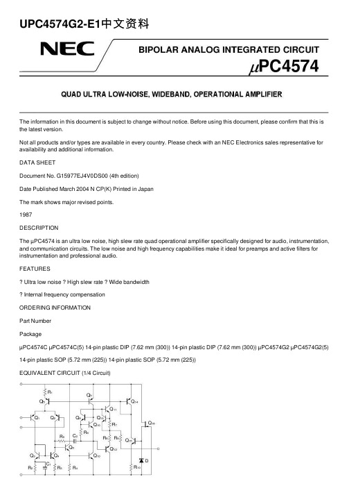
UPC4574G2-E1中⽂资料The information in this document is subject to change without notice. Before using this document, please confirm that this is the latest version.Not all products and/or types are available in every country. Please check with an NEC Electronics sales representative for availability and additional information.DATA SHEETDocument No. G15977EJ4V0DS00 (4th edition)Date Published March 2004 N CP(K) Printed in JapanThe mark shows major revised points.1987DESCRIPTIONThe µPC4574 is an ultra low noise, high slew rate quad operational amplifier specifically designed for audio, instrumentation, and communication circuits. The low noise and high frequency capabilities make it ideal for preamps and active filters for instrumentation and professional audio.FEATURESUltra low noise High slew rate Wide bandwidthInternal frequency compensationORDERING INFORMATIONPart NumberPackageµPC4574C µPC4574C(5) 14-pin plastic DIP (7.62 mm (300)) 14-pin plastic DIP (7.62 mm (300)) µPC4574G2 µPC4574G2(5) 14-pin plastic SOP (5.72 mm (225)) 14-pin plastic SOP (5.72 mm (225))EQUIVALENT CIRCUIT (1/4 Circuit)I I I NVVPIN CONFIGURATION (Top View)OUT 4I I4I N4V ?I N3I I3OUT 3OUT 1I I1I N1V +I N2I I2OUT 2PC4574C, 4574C(5), 4574G2, 4574G2(5)µData Sheet G15977EJ4V0DS2ABSOLUTE MAXIMUM RATINGS (T A = 25°C)Parameter SymbolRatings Unit Voltage between V +and V ? Note1V +V0.3 to +36VDifferential Input Voltage V ID ±30 V Input VoltageNote2V IV ??0.3 to V ++0.3 V Output VoltageNote3V OV ??0.3 to V + +0.3VC Package Note4570 mW Power Dissipation G2 PackageNote5P T 550 mW Output Short Circuit DurationNote610 sec Operating Ambient Temperature T A ?20 to +80 °C Storage TemperatureT stg55 to +125°CNotes 1. Reverse connection of supply voltage can cause destruction.2. The input voltage should be allowed to input without damage or destruction. Even during the transition periodof supply voltage, power on/off etc., this specification should be kept. The normal operation will establish when the both inputs are within the Common Mode Input Voltage Range of electrical characteristics.3. This specification is the voltage which should be allowed to supply to the output terminal from externalwithout damage or destructive. Even during the transition period of supply voltage, power on/off etc., this specification should be kept. The output voltage of normal operation will be the Output Voltage Swing of electrical characteristics.4. Thermal derating factor is –7.6 mW/°C when ambient temperature is higher than 50°C.5. Thermal derating factor is –5.5 mW/°C when ambient temperature is higher than 25°C.6. Pay careful attention to the total power dissipation not to exceed the absolute maximum ratings, Note 4 andNote 5.RECOMMENDED OPERATING CONDITIONSParameter Symbol MIN. TYP. MAX. UnitSupply Voltage V ± ±4 ±16 V Output Current I O±10 mASource Resistance R S 50k ?Capacitive Load (A V = +1)C L 100 pFµPC4574C, µPC4574G2±Notes 7. Input bias currents flow out from IC. Because each currents are base current of PNP-transistor on input stage.8.This current flows irrespective of the existence of use.Data Sheet G15977EJ4V0DS 3µPC4574C(5), µPC4574G2(5)±Notes 7. Input bias currents flow out from IC. Because each currents are base current of PNP-transistor on input stage.8.This current flows irrespective of the existence of use.4Data Sheet G15977EJ4V0DSMEASUREMENT CIRCUITFig.1 Total Harmonic Distortion Measurement CircuitnFig.3 Flat Noise Measurement Circuit (FLAT+JIS A)V O = 40 dB x V n100 V n =V O40 dBData Sheet G15977EJ4V0DS 5Data Sheet G15977EJ4V0DS6TYPICAL PERFORMANCE CHARACTERISTICS (T A = 25°C, TYP.) T A - Operating Ambient Temperature - ?CPOWER DISSIPATIONP T - T o t a l P o w e r D i s s i p a t i o n - m W800600400200020*********20406080100120110010 k 1 M 1 k 10100 k 10 Mf - Frequency - HzOPEN LOOP FREQUENCY RESPONSEA V - O p e n L o o p V o l t a g e G a i n - d BV ± = ±15 V202040608021.510.50?0.5?1?1.5?2T A - Operating Ambient Temperature - ?CINPUT OFFSET VOLTAGEV I O - I n p u t O f f s e t V o l t a g e - m V= ±15 VV ±each 5 samples data806040200?20550530510490470450T A - Operating Ambient Temperature - ?CINPUT BIAS CURRENTI B - I n p u t B i a s C u r r e n t - n A= ±15 VV ±f - Frequency - HzLARGE SIGNAL FREQUENCY RESPONSE V o m - O u t p u t V o l t a g e S w i n g - V p -p 01020301001 k 10 k 100 k 1 M 10 MV = ±15 V±R L = 10 k ?I O - Output Current - mAOUTPUT CURRENT LIMITV O - O u t p u t V o l t a g e - V±±5±10±15T A - Operating Ambient Temperature - ?CSUPPLY CURRENTI C C - S u p p l y C u r r e n t - m A12963204020060800V = ±15 V±SUPPLY CURRENTI C C - S u p p l y C u r r e n t - m A12963±10±20V - Supply Voltage - V±Data Sheet G15977EJ4V0DS7COMMON MODE INPUT VOLTAGE RANGE V I C M - C o m m o n M o d e I n p u t V o l t a g e R a n g e - V 20100±10±20V - Supply Voltage - V±VOLTAGE FOLLOWER PULSE RESPONSE V O - O u t p u t V o l t a g e - V10551002468t - Time - sµV = ±15 V ±A V = 1R L = 2 k ?INPUT NOISE VOLTAGE (FLAT + JIS A)V n - I n p u t N o i s e V o l t a g e - V r .m .s .1001010.1101001 k10 k100 kR S - Source Resistance - ?V = ±15 V±µf - Frequency - HzINPUT EQUIVALENT NOISE VOLTAGE DENSITY e n - I n p u t E q u i v a l e n t N o i s e V o l t a g e D e n s i t y - n V / H z20468100 1 k10 k 100 k10±R S = 100 VTOTAL HARMONIC DISTORTIONT H D - T o t a l H a r m o n i c D i s t o r t i o n - %10.0010.010.10.000110100 1 k10 k 100 kf - Frequency - HzV = ±15 V ±V O = 3 V r.m.s.A V = 1R L = 2 k ?Data Sheet G15977EJ4V0DS8PACKAGE DRAWINGS (Unit: mm)14-PIN PLASTIC DIP (7.62 mm (300))ITEM MILLIMETERS A 19.22±0.22.14 MAX.F I J D 1.32±0.12G 3.6±0.3C B 2.54 (T.P.)0.50±0.10R 0~15°H 0.51 MIN.K 7.62 (T.P.)L 6.4±0.23.554.3±0.2N 0.25NOTES1. Each lead centerline is located within 0.25 mm ofits true position (T.P.) at maximum material condition.2. ltem "K" to center of leads when formed parallel.P14C-100-300B1-3M 0.25+0.10?0.05Data Sheet G15977EJ4V0DS9ITEM B C I 14-PIN PLASTIC SOP (5.72 mm (225))D E G H J PMILLIMETERS 1.27 (T.P.)1.42 MAX.A 10.2±0.264.4±0.10.1±0.10.426.5±0.21.49+0.08?0.071.1±0.163°+7°?3°NOTEEach lead centerline is located within 0.1 mm ofits true position (T.P.) at maximum material condition.F 1.59+0.21?0.2K L M N 0.6±0.20.170.10.10+0.08?0.07S14GM-50-225B, C-6RECOMMENDED SOLDERING CONDITIONSThe µPC4574 should be soldered and mounted under the following recommended conditions.For soldering methods and conditions other than those recommended below, contact an NEC Electronics sales representative.For technical information, see the following website.Semiconductor Device Mount Manual (/doc/015a7dda76a20029bd642de6.html/pkg/en/mount/index.html)Type of Surface Mount DeviceµPC4574G2, 4574G2(5): 14-pin plastic SOP (5.72 mm (225))Process ConditionsSymbol Infrared Ray Reflow Peak temperature: 230°C or below (Package surface temperature),Reflow time: 30 seconds or less (at 210°C or higher),Maximum number of reflow processes: 1 time.IR30-00-1Vapor Phase Soldering Peak temperature: 215°C or below (Package surface temperature),Reflow time: 40 seconds or less (at 200°C or higher),Maximum number of reflow processes: 1 time.VP15-00-1Wave Soldering Solder temperature: 260°C or below, Flow time: 10 seconds or less,Maximum number of flow processes: 1 time,Pre-heating temperature: 120°C or below (Package surface temperature).WS60-00-1Partial Heating Method Pin temperature: 300°C or below,Heat time: 3 seconds or less (Per each side of the device).–Caution Apply only one kind of soldering condition to a device, except for "partial heating method", or thedevice will be damaged by heat stress.Type of Through-hole DeviceµPC4574C, 4574C(5): 14-pin plastic DIP (7.62 mm (300))Process ConditionsWave Soldering (only to leads) Solder temperature: 260°C or below, Flow time: 10 seconds or less.Partial Heating Method Pin temperature: 300°C or below,Heat time: 3 seconds or less (per each lead).Caution For through-hole device, the wave soldering process must be applied only to leads, and make sure that the package body does not get jet soldered.Data Sheet G15977EJ4V0DS10The information in this document is current as of March, 2004. The information is subject to change without notice. For actual design-in, refer to the latest publications of NEC Electronics data sheets or data books, etc., for the most up-to-date specifications of N EC Electronics products. N ot all products and/or types are available in every country. Please check with an N EC Electronics sales representative for availability and additional information.No part of this document may be copied or reproduced in any form or by any means without the prior written consent of NEC Electronics. NEC Electronics assumes no responsibility for any errors that may appear in this document.NEC Electronics does not assume any liability for infringement of patents, copyrights or other intellectual property rights of third parties by or arising from the use of NEC Electronics products listed in this document or any other liability arising from the use of such products. No license, express, implied or otherwise, is granted under any patents, copyrights or other intellectual property rights of NEC Electronics or others.Descriptions of circuits, software and other related information in this document are provided for illustrative purposes in semiconductor product operation and application examples. The incorporation of these circuits, software and information in the design of a customer's equipment shall be done under the full responsibility of the customer. NEC Electronics assumes no responsibility for any losses incurred by customers or third parties arising from the use of these circuits, software and information.While NEC Electronics endeavors to enhance the quality, reliability and safety of NEC Electronics products, customers agree and acknowledge that the possibility of defects thereof cannot be eliminated entirely. To minimize risks of damage to property or injury (including death) to persons arising from defects in NEC Electronics products, customers must incorporate sufficient safety measures in their design, such as redundancy, fire-containment and anti-failure features.NEC Electronics products are classified into the following three quality grades: "Standard", "Special" and "Specific".The "Specific" quality grade applies only to NEC Electronics products developed based on a customer-designated "quality assurance program" for a specific application. The recommended applications of an NEC Electronics product depend on its quality grade, as indicated below. Customers must check the quality grade of each NEC Electronics product before using it in a particular application."Standard":Computers, office equipment, communications equipment, test and measurement equipment, audioand visual equipment, home electronic appliances, machine tools, personal electronic equipment and industrial robots. "Special":Transportation equipment (automobiles, trains, ships, etc.), traffic control systems, anti-disastersystems, anti-crime systems, safety equipment and medical equipment (not specifically designed for life support). "Specific":Aircraft, aerospace equipment, submersible repeaters, nuclear reactor control systems, lifesupport systems and medical equipment for life support, etc.The quality grade of NEC Electronics products is "Standard" unless otherwise expressly specified in NEC Electronics data sheets or data books, etc. If customers wish to use NEC Electronics products in applications not intended by NEC Electronics, they must contact an NEC Electronics sales representative in advance to determine NEC Electronics' willingness to support a given application.(Note)(1)"NEC Electronics" as used in this statement means NEC Electronics Corporation and also includes itsmajority-owned subsidiaries.(2)"NEC Electronics products" means any product developed or manufactured by or for NEC Electronics (asdefined above).M8E 02. 11-1。
无线路由器CPU闪存内存芯片列表

TR-966D
RealtekRTL8305SC
TR-965DA
EN29LV160AB闪存2MB
S29AL908D70TE102不明芯片
TL-R480T
TL-R4000
TL-R480T÷
TL-R488T
TL-R4000+
TL-SG3109
TL-SG3216
TL-SG3224
TL-SG3248
TL-SL3428
TL-SL3452
TL-SG2109WEB
IntelFWIXP420BB(CPU)+MarVell88E6063(Switch)
Marvell88E6092(MAC)+88E1111(PHY)+88E6218(CPU)
Marvell88E6092(MAC)+88E1111(PHY)+88E6218(CPU)
Marvell88E6182+88E6092(MAC)+88E1111(PHY)+88E6218(CPU)
Marvell88E6182+88E6092(MAC)+88E1111(PHY)+88E6218(CPU)
品牌规格
cpu
主频
闪存/内存
无线芯片
参考价
迅捷FVVR300T+
AtherosAR9132
400MHZ
4/32
Atheros
AR9103
90
水星MWR300T+
(旧款长方形的)
AtherosAR9132
400MHZ
4/32Vl版新款可能有缩水
Atheros
AR9103
90
Victron EM24 Ethernet 三相功率能量计手册说明书

ENGLISHEnergy Meter ManualEM24 Ethernetrev 05 - 08/2023This manual is also available in HTML5Table of Contents1. Introduction (1)1.1. Features (1)2. Installation and configuration (2)2.1. AC wiring (2)2.1.1. Configuration options (2)2.1.2. System examples (2)2.2. GX device configuration (4)3. FAQ (6)The Victron EM24 Ethernet is a standard device to measure the power and energy of a 3-phase application, for example at the distribution box or to measure the output of a PV Inverter, AC Genset or the output of an inverter and inverter/charger.Its data will be displayed on a GX device and our VRM portal.1.1. FeaturesThe EM24 Ethernet can be configured for four different roles in a GX device such as the Cerbo GX:1.As a Grid meter and used as control input for an ESS System.2.To measure the output of a PV Inverter.3.To measure the output of a AC Genset.4.As a AC meter to measure the output of an inverter or inverter/charger.It offers one option for connection to a GX device:1. A wired ethernet connection to the local network in such a way that the GX device can reach it.2.1. AC wiring2.1.1. Configuration optionsThe configuration option of either Grid Meter, PV Inverter, Generator or AC Meter is set in the GX device. For details on GX device configuration see the GX device configuration [4] chapter. This selection will effect how the system should be wired and how the information received from the meter is displayed on the screen.See below diagrams for the different wiring options:2.1.2. System examplesExample diagramsL1L2L3NPEL1L2L3NPEEM24 3-phase wiringWhen used to measure a PV Inverter, terminals 1, 4 and 7 should face the PV inverter to ensure correctdirection of current and power.Single-phase, single functionL1NL1NEM24 connected as a single-phase, single function grid meterNote the jumper between terminals 1 and 4. You do not need this connection if you have the version AV2 of the sensor.The diagrams show the wiring when used as a grid meter.To measure a single-phase PV inverter in a 3-phase system, connect all 3 phases to the grid phasing terminals (3, 6 and 9). Now you can chose on which phase you want the PV inverter by connecting the L1 line of the PV inverter to terminal 1, 4 or 7.Single-phase, dual functionIf you want to use a three-phase meter in a single-phase installation to measure the grid on one input of the meter and the output of the PV inverter on another input of the energy meter, make sure that the energy meter uses L1 and the PV inverter uses L2.Front selectorChange the front selector so it is not in the locked state. This allows it to be automatically configured by the GX Device. The front selector is located next to the display as indicated in the image above.2.2. GX device configurationAfter proper connection and powering up, the meter(s) will be visible on the GX device in the Settings → Energy meters menu:Single Energy Meter in the Energy meters menu Two Energy Meters in the Energy meters menuAfter selecting an Energy Meter, you have to set the Role and Phase type. Press the space bar or right click to get to the Phase type and Role menu:For the ET112 only Single phase option is displayed Depending on the application, the role is set hereSelect either Role or Phase type and press the space bar to make changes:Select the Role according to the application Selection menu for Single and Multi phase typeSingle-phase, single function and single-phase, dual function mode setup:Single-phase, single function Single-phase, dual function to measure grid on L1 and a PVInverter on L2After all settings have been made, the Energy Meter now appears with the relevant data in the device list of the GX device:Or configured to measure energy consumption from the grid Energy meter set to measure AC loads on the AC output ofthe inverter/chargerRight-click or press the spacebar to get to the Energy Meter overview with all relevant data on energy consumption and its generation in all phases. At the bottom of the menu, the role of the Energy Meter can be set via the Setup menu. The data used for communication can be read out via the Device menu. You can also set up a custom name for the Energy Meter there:Detailed overview page of a 3-phase Grid meter Always be informed about all details, to the second Custom name configuration Quickly change rolesQ1: Can I combine three ET112s for a 3-phase system?No. Use a real 3-phase meter.Q2: Can I use other meters, for example from other brands?No.Q3: I already have a Fronius SmartGrid meter, can I use that?No.Q4: What are the differences between the various 3-phase meters?•EM540 - REL200100100 - Carlo Gavazzi EM540DINAV23XS1X•ET112 - REL300100000 - Carlo Gavazzi ET112-DIN.AV01.X.S1.X•ET340 - REL300300000 - Carlo Gavazzi ET340-DIN.AV23.X.S1.XDifferences:•The ET meters have no display. The only thing they have is an LED, which blinks in case of active communication.•The ET meters have two RJ45 sockets, but they are not used with the Victron RS485 to USB interface. Note the possible confusion because of yet another RJ45 socket in the Victron world though. Don't mix that with VE.Bus, VE.Can or . Besides the RJ45 sockets, the meters still also have screw terminals access below the sockets for the RS485 wiring, which is how we advise to connect a meter to the RS485 to USB interface and then a GX device.•Since there is no display, the modbus address can no longer be changed on the meter. Combining multiple of those meters on one RS485 network is therefore not supported by Victron. You are advised to use multiple RS485 to USB interfaces.3-phase meter only:•Measuring energy from single-phase PV Inverter on the second phase of a 3-phase meter actually works.Q5: Will you keep shipping both 3-phase meters? (ET340 & EM540)Yes. There are still situations suitable for each. See Q8.Q6: Can I buy those meters directly from Carlo Gavazzi instead of from you?Yes. That is also why we make no secret of the CG part numbers.Q7: I want to use Current Transformers (CTs), is that possible?Yes. You can buy a CG EM24DINAV53DISX or a CG EM530DINAV53XS1X directly from Carlo Gavazzi or one of their distributors. Even though Victron does not stock that type of meter, we do support it in our software.Q8: What’s the difference between ET340 and EM540 in 3-phase systems?These meters have a different way of calculating the total of energy imported and exported.In the ET340, the energy imported and exported is counted at each individual phase and then the Total is provided from the sum of those values.In the EM540, the energy imported and exported is counted as a total power, with net differential readings from each phase cancelling each other out.Which Energy Meter is most suitable depends on the measuring configuration in your country. It is most common in Austria and Germany for example to only be billed for the total in a 3-phase system. So it is more accurate to use an EM540 to match the billing.So if you are exporting from one phase and importing from another phase after the energy meter, but before the billing meter, then you will not be charged for this, and the meter should not count it as an import and an export.This is also how Victron’s phase compensation feature works, to make the most of the cost savings for an ESS system when there is a differential in generation and load across different phases.Q9: Can I use an isolated USB-RS485 interface?Yes. The interfaces we sell are non isolated; suitable for most use cases.In case an isolated one is needed; purchase it directly from Hjelmslund Electronics.•USB485-STIXL : Isolated USB to RS485 converterQ10: Can I use Victron Energy Meters instead of a Victron Inverter/Charger to make use of a GX device (e.g. Cerbo GX), VRM and other features?Energy Meters are intended to supplement a Victron Inverter/Charger in the system. Energy Meters are currently limited in their potential applications. Each Energy Meter is only intended to provide a specific piece of additional information - total loads on AC input and grid import/export, or AC PV inverter and AC generator production without network communications.However, it is perfectly possible to initially use just a GX device together with an Energy Meter to determine and record the consumption, for example of houses/buildings, heating systems with heat pumps, ventilating and air conditioning or production facilities. Afterwards, the collected data can be evaluated and a decision can be made about the dimensioning of the required Victron inverter/charger(s), the solar system and the type, size and number of batteries.With GX device firmware version 2.80 and later, they can also be used for other purposes e.g. to measure specific, arbitrary AC loads or circuits for example. But this should not be considered a replacement to having a Victron Inverter/Charger. Attempting to use other brand battery inverters and trying to substitute their lack of data connectivity to the GX device by using Energy Meters will not work as expected.。
UPC3241TB-E3-A;UPC3241TB-A;UPC3241TB-EVAL-A;中文规格书,Datasheet资料

MMIC
MEDIUM
OUTPUT
POWER
PO (sat) (dBm) + 9.0 (0.9 GHz) + 8.5 (1.9 GHz) + 11.0 (0.9 GHz) + 8.0 (1.9 GHz) + 12.5 (0.9 GHz) + 11.0 (1.5 GHz) + 9.5 (0.9 GHz) + 9.0 (1.9 GHz) + 9.0 (2.4 GHz) + 11.0 (0.9 GHz) + 10.5 (1.9 GHz) + 10.0 (2.4 GHz) + 12.5 (1.0 GHz) + 10 (2.2 GHz)
This device exhibits low noise figure and high power gain characteristics. This IC is manufactured using our UHS0 (Ultra High Speed Process) bipolar process.
Parameter Supply Voltage Total Circuit Current Power Dissipation Operating Ambient Temperature Storage Temperature Input Power Symbol VCC ICC PD TA Tstg Pin TA = +25°C Conditions TA = +25°C, pin 4 and 6 TA = +25°C, pin 4 and 6 TA = +85C Note Ratings 4.0 55 270 40 to +85 55 to +150 10 Unit V mA mW °C °C dBm
G.SKILL DDR3内存型号参考清单说明书

G.SKILL F3-3000C12Q-16GTXDG16GB (4 x 4GB )SS--- 1.65V●●●G.SKILL F3-2933C12D-8GTXDG8GB (2 x 4GB )SS--12-14-14-35 1.65V●●G.SKILL F3-2933C12Q-16GTXDG16GB (4 x 4GB )SS--12-14-14-35 1.65V●●●G.SKILL F3-2800C11Q-16GTXD(XMP)16GB(4GBx4)DS--11-13-13-35 1.65V●●CORSAIR CMD16GX3M4A2666C11 (XMP)4GB DS--11-13-13-35 1.65V●●●G.SKILL F3-2666C11Q-16GTXD(XMP)16GB(4GBx4)DS--11-13-13-35 1.65V●●●Team TXD34G2666HC11CBK8GB ( 2x 4GB )SS--11-13-13-35 1.65V●●●Team TXD38G2666HC11CBK16GB ( 2x 8GB )DS--11-13-13-35 1.65V●●G.SKILL F3-2600CL10Q-16GBZMD(XMP)16GB(4x 4GB)DS--10-12-12-31 1.65V●●G.SKILL F3-2600CL11Q-32GBZHD(XMP)32GB(8GBX4)DS--11-13-13-35 1.65V●●ADATA AX3U2600GW8G1116GB ( 2x 8GB )DS--11-13-13-35 1.65V●●CORSAIR CMGTX8(XMP)8GB (2GBx 4)SS--10-12-10-27 1.65V●●G.SKILL F3-2400C10D-8GTX(XMP)8GB(2x 4GB)SS--10-12-12-31 1.65V●●●G.SKILL F3-19200CL11Q-16GBZHD(XMP1.3)16GB ( 4GB x4 )DS--11-11-11-31 1.65V●●G.SKILL F3-19200CL 10Q-32GBZHD(XMP)8GB DS--10-12-12-31 1.65V●●●KINGMAX FLLE88F-C8KKAA HAIS(XMP)2GB SS--10-11-10-30 1.8V●●●KINGSTON KHX24C11T2K2/8X(XMP)4GB DS--- 1.65V●●●ADATA AX3U2400GW8G1116GB ( 2x 8GB )DS--11-13-13-35 1.65V●●ADATA AX3U2400G4G10-DG2(XMP)4GB DS--10-12-12-31 1.65V●●Team TXD38G2400HC10QBK8GB DS--10-12-12-31 1.65V●●●KINGSTON KHX2250C9D3T1K2/4GX(XMP)4GB ( 2x 2GB )DS--- 1.65V●●●GEIL GET34GB2200C9DC(XMP)2GB DS--9-10-9-28 1.65V●●GEIL GET38GB2200C9ADC(XMP)4GB DS--9-11-9-28 1.65V●●KINGMAX FLKE85F-B8KJAA-FEIS(XMP)2GB DS--- 1.5V●●CORSAIR CMT16GX3M4X2133C9(XMP 1.3)16GB ( 4GB x4 )DS--9-11-10-27 1.50V●●●CORSAIR CMT4GX3M2A2133C9(XMP)4GB(2x 2GB)DS--9-10-9-24 1.65V●●●CORSAIR CMT4GX3M2B2133C9(XMP)4GB(2x 2GB)DS--9-10-9-27 1.50V●CORSAIR CMT8GX3M2B2133C9(XMP)8GB ( 4GB x 2)DS--9-11-9-27 1.50V●●●G.SKILL F3-17000CL9Q-16GBZH(XMP1.3)16GB ( 4GB x4 )DS--9-11-10-28 1.65V●●●G.SKILL F3-17000CL11Q2-64GBZLD(XMP)8GB DS--11-11-11-31 1.5V●●●G.SKILL F3-2133C11Q-32GZL(XMP)8GB DS--11-11-11-31 1.5V●●●GEIL GE34GB2133C9DC(XMP)2GB DS--9-9-9-28 1.65V●●GEIL GU34GB2133C9DC(XMP)4GB(2 x 2GB)DS--9-9-9-28 1.65V●●KINGSTON KHX2133C11D3K4/16GX(XMP)16GB ( 4GB x4 )DS--- 1.65V●●●KINGSTON KHX2133C11D3T1K2/16GX(XMP)16GB(8GB x 2)DS--- 1.6V●●●KINGSTON KHX21C11T1BK2/16X(XMP)16GB(8GBx2)DS--- 1.6V●●●KINGSTON KHX2133C9AD3T1K2/4GX(XMP)4GB ( 2x 2GB )DS--- 1.65V●●●KINGSTON KHX2133C9AD3X2K2/4GX(XMP)4GB(2 x 2GB)DS--9-11-9-27 1.65V●●●KINGSTON KHX2133C9AD3T1K4/8GX(XMP)8GB(4 x 2GB)DS--9-11-9-27 1.65V●KINGSTON KHX21C11T1BK2/8X(XMP)8GB(4GBx2)DS--- 1.6V●●●KINGSTON KHX2133C9AD3T1FK4/8GX(XMP)8GB(4x 2GB)DS--- 1.65V●●KINGSTON KHX21C11T3K4/32X8GB DS--- 1.65V●●●ADATA AX3U2133XW8G1016GB ( 2x 8GB )DS--10-11-11-30 1.65V●●●ADATA AX3U2133XC4G10-2X(XMP)4GB DS--10-11-11-30 1.65V●●●ADATA AX3U2133XW8G10-2X(XMP)8GB DS--10-11-11-30 1.65V●●●Team TXD34096M2133HC11-L4GB SS--- 1.5V●●●Team TLD38G2133HC11ABK8GB DS--11-11-11-31 1.65V●●●Apacer78.AAGD5.9KD(XMP)6GB(3 x 2GB)DS--9-9-9-27 1.65V●●●CORSAIR CMZ4GX3M2A2000C10(XMP)4GB(2 x 2GB)SS--10-10-10-27 1.50V●●●CORSAIR CMT6GX3M3A2000C8(XMP)6GB(3 x 2GB)DS--8-9-8-24 1.65V●●●G.SKILL F3-16000CL9D-4GBFLS(XMP)4GB(2 x 2GB)DS--9-9-9-24 1.65V●●G.SKILL F3-16000CL9D-4GBTD(XMP)4GB(2 x 2GB)DS--9-9-9-27 1.65V●●G.SKILL F3-16000CL6T-6GBPIS(XMP)6GB (3x 2GB )DS--6-9-6-24 1.65V●●●GEIL GUP34GB2000C9DC(XMP)4GB(2 x 2GB)DS--9-9-9-28 1.65V●●KINGSTON KHX2000C9AD3T1K2/4GX(XMP)4GB ( 2x 2GB )DS--- 1.65V●●KINGSTON KHX2000C9AD3W1K2/4GX(XMP)4GB ( 2x 2GB )DS--- 1.65V●●KINGSTON KHX2000C9AD3W1K3/6GX(XMP)6GB ( 3x 2GB )DS--- 1.65V●●KINGSTON KHX2000C9AD3T1K3/6GX(XMP)6GB (3x 2GB )DS--- 1.65V●●CORSAIR CMT4GX3M2A1866C9(XMP)4GB(2 x 2GB)DS--9-9-9-24 1.65V●●●CORSAIR CMT6GX3MA1866C9(XMP)6GB(3 x 2GB)DS--9-9-9-24 1.65V●●CORSAIR CMZ8GX3M2A1866C9(XMP)8GB(2 x 4GB)DS--9-10-9-27 1.50V●●●CRUCIAL BLE4G3D1869DE1TXO.16FMD(XMP)4GB DS--9-9-9-27 1.5V●●●CRUCIAL BLT4G3D1869DT1TX0.13FKD(XMP)4GB DS--9-9-9-27 1.5V●●●CRUCIAL BLT4G3D1869DT2TXOB.16FMR(XMP)4GB DS--9-9-9-27 1.5V●●G.SKILL F3-14900CL9Q-16GBZL(XMP1.3)16GB ( 4GB x4 )DS--9-10-9-28 1.5V●●●G.SKILL F3-14900CL10Q2-64GBZLD(XMP1.3)64GB ( 8GBx 8 )DS--10-11-10-30 1.5V●●●G.SKILL F3-14900CL9D-8GBXL(XMP)8GB(2 x 4GB)DS--9-10-9-28 1.5V●●G.SKILL F3-14900CL9Q-8GBXL(XMP)8GB(2GBx4)DS--9-9-9-24 1.6V●●●KINGSTON KHX1866C9D3K4/16GX(XMP)16GB ( 4GB x4 )DS--- 1.65V●●●KINGSTON KHX1866C11D3P1K2/8G8GB ( 4GB x 2)DS--- 1.5V●●●KINGSTON KHX1866C9D3K2/8GX(XMP)8GB(4GBX2)DS--- 1.65V●●●KINGSTON KHX18C10T3K4/32X8GB DS--- 1.5V●●●ADATA AX3U1866XW8G1016GB ( 2x 8GB )DS--10-11-10-30 1.5V●●●Team TLD38G1866HC10SBK8GB DS--10-11-10-30 1.5V●●●APACER4GB UNB PC3-12800 CL114GB SS APACER AM5D6008BQQSCK--●●●Apacer78.B1GE3.9L10C4GB DS Apacer KZZC AM5D5908DEQSCK--●●●APACER8GB UNB PC3-12800 CL118GB DS APACER AM5D6008BQQSCK--●●●CORSAIR CMD12GX3M6A1600C8(XMP)12GB(6x2GB)DS--8-8-8-24 1.65V●●●CORSAIR CMZ32GX3M4X1600C10(XMP)32GB(8GBx4)DS--10-10-10-27 1.50V●●●CORSAIR CMP4GX3M2A1600C8(XMP)4GB(2 x 2GB)DS--8-8-8-24 1.65V●●●CORSAIR CMP4GX3M2A1600C9(XMP)4GB(2 x 2GB)DS--9-9-9-24 1.65V●●●CORSAIR CMP4GX3M2C1600C7(XMP)4GB(2 x 2GB)DS--7-8-7-20 1.65V●●●CORSAIR CMX4GX3M2A1600C9(XMP)4GB(2 x 2GB)DS--9-9-9-24 1.65V●●●CORSAIR TR3X6G1600C8 G(XMP)6GB(3 x 2GB)DS--8-8-8-24 1.65V●●●CORSAIR TR3X6G1600C8D G(XMP)6GB(3 x 2GB)DS--8-8-8-24 1.65V●●●CORSAIR TR3X6G1600C9 G(XMP)6GB(3 x 2GB)DS--9-9-9-24 1.65V●●●CORSAIR CMP8GX3M2A1600C9(XMP)8GB(2 x 4GB)DS--9-9-9-24 1.65V●●●CORSAIR CMZ8GX3M2A1600C7R(XMP)8GB(2 x 4GB)DS--7-8-7-20 1.50V●●CORSAIR CMX8GX3M4A1600C9(XMP)8GB(4 x 2GB)DS--9-9-9-24 1.65V●●●CORSAIR CMZ8GX3M1A1600C10(XMP)8GB DS--10-10-10-27 1.50V●●●Crucial BL25664BN1608.16FF(XMP)6GB(3 x 2GB)DS--- 1.65V●●●G.SKILL F3-12800CL7D-4GBRH(XMP)4GB(2 x 2GB)SS--7-7-7-24 1.6V●●●G.SKILL F3-12800CL7D-4GBRM(XMP)4GB(2 x 2GB)DS--7-8-7-24 1.6V●●●G.SKILL F3-12800CL8D-4GBRM(XMP)4GB(2 x 2GB)DS--8-8-8-24 1.60V●●G.SKILL F3-12800CL9D-4GBECO(XMP)4GB(2 x 2GB)DS--9-9-9-24XMP 1.35V●●G.SKILL F3-12800CL9D-4GBRL(XMP)4GB(2 x 2GB)DS--9-9-9-24 1.5V●●●G.SKILL F3-12800CL7D-8GBRH(XMP)8GB(2 x 4GB)DS--7-8-7-24 1.6V●●●G.SKILL F3-12800CL8D-8GBECO(XMP)8GB(2 x 4GB)DS--8-8-8-24XMP 1.35V●●●G.SKILL F3-12800CL9D-8GBRL(XMP)8GB(2 x 4GB)DS--9-9-9-24 1.5V●●●G.SKILL F3-12800CL10S-8GBXL(XMP)8GB DS--10-10-10-30-●●●GEIL GET316GB1600C9QC(XMP)16GB ( 4x 4GB )DS--9-9-9-28 1.6V●●●HYNIX HMT351U6CFR8C-PB4GB DS HYNIX H5TQ2G83CFR PBC--●●●KINGMAX FLGE85F-B8KJ9A FEIS(XMP)2GB DS--- 1.5V●●●KINGMAX FLGE85F-B8MF7 MEEH(XMP)2GB DS--7 1.8V/1.9V●KINGSTON KHX1600C9D3P1K2/4G4GB(2 x 2GB)SS--- 1.5V●●●KINGSTON KHX1600C9D3K3/12GX(XMP)12GB(3x4GB)DS--9-9-9-27 1.65V●●●KINGSTON KHX1600C9D3T1BK3/12GX(XMP)12GB(3x4GB)DS--9-9-9-27 1.65V●●KINGSTON KHX1600C9D3K4/16GX(XMP)16GB ( 4GB x4 )DS--- 1.65V●●●KINGSTON KHX16C9K2/1616GB(8GBx2)DS--- 1.5V●●KINGSTON KHX1600C9AD3/2G2GB DS--- 1.65V●●●KINGSTON KVR1600D3N11/2G-ES2GB DS KTC D1288JPNDPLD9U11-11-11-28 1.35V-1.5V●●●KINGSTON KHX1600C7D3K2/4GX(XMP)4GB ( 2x 2GB )DS--- 1.65V●●●KINGSTON KHX1600C8D3K2/4GX(XMP)4GB(2 x 2GB)DS--8 1.65V●●●KINGSTON KHX1600C8D3T1K2/4GX(XMP)4GB(2 x 2GB)DS--8 1.65V●●●KINGSTON KHX1600C9D3K2/4GX(XMP)4GB(2 x 2GB)DS--9 1.65V●●●KINGSTON KHX1600C9D3LK2/4GX(XMP)4GB(2 x 2GB)DS--9XMP 1.35V●●●KINGSTON KHX1600C9D3X2K2/4GX(XMP)4GB(2 x 2GB)DS--9-9-9-27 1.65V●●●KINGSTON KVR16N11/4(矮版)4GB DS KINGSTON D2568GEROPGGBU- 1.5V●●●KINGSTON KHX1600C9D3T1K3/6GX(XMP)6GB ( 3x 2GB )DS--- 1.65V●●KINGSTON KHX1600C9D3K3/6GX(XMP)6GB(3 x 2GB)DS--9 1.65V●●KINGSTON KHX1600C9D3T1BK3/6GX(XMP)6GB(3 x 2GB)DS--9-9-9-27 1.65V●●●KINGSTON KHX1600C9D3K2/8GX(XMP)8GB(2 x 4GB)DS--- 1.65V●●KINGSTON KHX1600C9D3P1K2/8G8GB(2 x 4GB)DS--- 1.5V●●●KINGSTON KHX16C10B1K2/16X(XMP)8GB DS--- 1.5V●●●KINGSTON KHX16C9P1K2/16(XMP)8GB DS--- 1.5V●●●PSC AL9F8L93B-GN2E4GB SS PSC XHP284C3G-M--●●●PSC ALAF8L93B-GN2E8GB DS PSC XHR425C3G-M--●●●Transcend8G DDR3 1600 DIMM CL118GB DS SEC 222 HYKO6MD9639W--●●●Transcend8G DDR3 1600 DIMM CL118GB DS Transcend E223X8BO648S--●●●ADATA AD3U1600C2G11-B2GB SS-N/A--●●●ADATA AD3U1600W4G11-B4GB SS ADATA F209X8BR6413--●●●ADATA AX3U1600GW8G916GB ( 2x 8GB )DS--9-9-9-24 1.5V●●●ADATA AX3U1600W8G1116GB ( 2x 8GB )DS--11-11-11-28 1.5V●●●ADATA AXDU1600GW8G9B16GB ( 2x 8GB )DS--11-11-11-28 1.5V●●●ADATA AD3U1600C4G11-B4GB DS-N/A--●●●ADATA AD3U1600W8G11-B8GB DS ADATA F211X8B0640A--●●SanMax SMD-4G68HP-16KZ4GB DS HYNIX H5TQ2G83BFR PBC--●●●TEAM TED34G1600HC11BK4GB DS--11-11-11-28-●●●TEAM TLD34G1600HC9BK(XMP)4GB DS--9-9-24 1.5V●●●Team TED38G1600HC11BK8GB DS--11-11-11-28-●●●A-DATA AD3U1333C2G92GB SS A-DATA3CCD-1509HNA1126L--●●●A-DATA AX3U1333C2G9-BP2GB SS----●●●A-DATA AD31333G002GMU2GB DS--8-8-8-24 1.65-1.85V●●Apacer78.A1GC6.9L12GB DS Apacer AM5D5808DEWSBG--●●●Apacer78.A1GC6.9L12GB DS Apacer AM5D5808FEQSBG9-●●●Apacer AU02GFA33C9NBGC2GB DS Apacer AM5D5808APQSBG--●●●Apacer78.B1GDE.9L10C4GB DS Apacer AM5D5908CEHSBG--●●●CORSAIR TR3X6G1333C9 G6GB(3x 2GB)SS--9-9-9-24 1.50V●●●CORSAIR CMD24GX3M6A1333C9(XMP)24GB(6x4GB)DS--9-9-9-24 1.60V●●CORSAIR TW3X4G1333C9D G4GB(2 x 2GB)DS--9-9-9-24 1.50V●●●CORSAIR CM3X4GA1333C9N24GB DS CORSAIR256MBDCJGELC04011369-9-9-24-●●●CORSAIR CMX4GX3M1A1333C94GB DS--9-9-9-24 1.50V●●●CORSAIR CMD8GX3M4A1333C78GB(4 x 2GB)DS--7-7-7-20 1.60V●●●Crucial CT25664BA1339.16FF2GB DS Micron9KF27D9KPT9-●●●Crucial BL25664BN1337.16FF (XMP)6GB(3 x 2GB)DS--7-7-7-24 1.65V●●●ELPIDA EBJ21UE8EDF0-DJ-F2GB DS ELPIDA J1108EDSE-DJ-F- 1.35V(low voltage)●●●G.SKILL F3-10666CL8D-4GBECO(XMP)4GB(2 x 2GB)DS--8-8-8-8-24XMP 1.35V●●●G.SKILL F3-10666CL7T-6GBPK(XMP)6GB(3 x 2GB)DS--7-7-7-18 1.5~1.6V●G.SKILL F3-10666CL7D-8GBRH(XMP)8GB(2 x 4GB)DS--7-7-7-21 1.5V●●●GEIL GG34GB1333C9DC4GB(2 x 2GB)DS GEIL GL1L128M88BA12N9-9-9-24 1.3V(low voltage)●●●GEIL GV34GB1333C9DC4GB(2 x 2GB)DS--9-9-9-24 1.5V●●●GEIL GVP34GB1333C7DC4GB(2 x 2GB)DS--7-7-7-24 1.5V●●●Hynix HMT325U6BFR8C-H92GB SS Hynix H5TQ2G83BFRH9C--●●●Hynix HMT125U6TFR8A-H92GB DS Hynix H5TC1G83TFRH9A- 1.35V(low voltage)●●●Hynix HMT351U6BFR8C-H94GB DS Hynix H5TQ2G83BFRH9C--●●●KINGMAX FLFE85F-C8KF9 CAES2GB SS KINGMAX KFC8FMFXF-DXX-15A--●●●KINGMAX FLFE85F-C8KL9 NAES2GB SS KINGMAX KFC8FNLXF-DXX-15A--●●●KINGMAX FLFE85F-C8KM9 NAES2GB SS KINGMAX KFC8FNMXF-BXX-15A--●●KINGMAX FLFE85F-B8KL9 NEES2GB DS KINGMAX KKB8FNWBFGNX-26A--●●●KINGMAX FLFF65F-C8KL9 NEES4GB DS KINGMAX KFC8FNLXF-DXX-15A--●●●KINGMAX FLFF65F-C8KM9 NEES4GB DS KINGMAX KFC8FNMXF-BXX-15A--●●●KINGSTON KVR1333D3N9/2G(矮版)2GB SS Hynix H5TQ2G83AFRH9C9-●●●KINGSTON KVR1333D3S8N9/2G2GB SS Micron IID77 D9LGK- 1.5V●●●KINGSTON KVR1333D3S8N9/2G-SP(矮版)2GB SS ELPIDA J2108BCSE-DJ-F- 1.5V●●●KINGSTON KVR1333D3N9/2G(矮版)2GB DS ELPIDA J1108BFBG-DJ-F9 1.5V●●●KINGSTON KVR1333D3N9/2G-SP(矮版)2GB DS KTC D1288JEMFNGD9U- 1.5V●●●KINGSTON KVR1333D3N9/2G-SP(矮版)2GB DS KINGSTON D1288JPSFPGD9U- 1.5V●●●KINGSTON KHX1333C7D3K2/4GX(XMP)4GB(2 x 2GB)DS--7 1.65V●●●KINGSTON KHX1333C9D3UK2/4GX(XMP)4GB(2 x 2GB)DS--9XMP 1.25V●●KINGSTON KVR1333D3N9/4G(矮版)4GB DS ELPIDA J2108BCSE-DJ-F- 1.5V●●●KINGSTON KVR1333D3N9/4G4GB DS KTC D2568JENCNGD9U- 1.5V●●●KINGSTON KVR1333D3N9/4G4GB DS Hynix H5TQ2G83AFR--●●●KINGSTON KVR1333D3N9/4G-SP(矮版)4GB DS KINGSTON D2568JENCPGD9U- 1.5V●●●Micron MT8JTF25664AZ-1G4D12GB SS Micron OJD12D9LGK--●●●Micron MT8JTF25664AZ-1G4M12GB SS MICRON IJM22 D9PFJ--●●●Micron MT16JTF51264AZ-1G4D14GB DS Micron OLD22D9LGK--●●●NANYA NT4GC64B8HG0NF-CG4GB DS NANYA NT5CB256M8GN-CG--●●●PSC AL8F8G73F-DJ22GB DS PSC A3P1GF3FGF--●●●SAMSUNG M378B5773DH0-CH92GB SS SAMSUNG K4B2G0846D--●●●SAMSUNG M378B5673FH0-CH92GB DS SAMSUNG K4B1G0846F--●●●SAMSUNG M378B5273CH0-CH94GB DS SAMSUNG K4B2G0846C--●●●SAMSUNG M378B1G73AH0-CH98GB DS SAMSUNG K4B4G0846A-HCH9--●●Super Talent W1333UB2GS2GB DS SAMSUNG K4B1G0846F9-●●●Super Talent W1333UB4GS4GB DS SAMSUNG K4B2G0846C--●●●Super Talent W1333UX6GM6GB(3x 2GB)DS Micron0BF27D9KPT9-9-9-24 1.5V●●●Transcend JM1333KLN-2G2GB SS HYNIX H5TQ2G83BZRH9C--●●●Transcend8G DDR3 1333 DIMM CL98GB DS Transcend E207X8BO643Y--●●Transcend8G DDR3 1333 DIMM CL98GB DS-N/A--●●●KINGSTEK KSTD3PC-106002GB SS MICRON PE911-125E--●●●TEAM TED34G1333HC9BK4GB DS--9-9-9-24-●●TEAM TED38G1333HC9BK8GB DS--9-9-9-24-●●●Crucial CT25664BA1067.16FF2GB DS Micron9HF22D9KPT7-●●●ELPIDA EBJ21UE8EDF0-AE-F2GB DS ELPIDA J1108EDSE-DJ-F- 1.35V(low voltage)●●●KINGSTON KVR1066D3N7/2G2GB DS ELPIDA J1108BFSE-DJ-F- 1.5V●●●KINGSTON KVR1066D3N7/4G4GB DS Hynix H5TQ2G83AFR7 1.5V●●●4 DIMM Slots• 1 DIMM: Supports one module inserted in any slot as Single-channel memory configuration• 2 DIMM: Supports one pair of modules inserted into eithor the yellow slots or the dark brown slots as one pair of Dual-channel memory configuration• 4 DIMM: Supports 4 modules inserted into both the yellow and dark brown slots as two pairs of Dual-channel memory configuration-When installing total memory of 4GB capacity or more, Windows 32-bit operation system may only recognize less than 3GB. Hence, a total installed memory of less than 3GB is recommended.-It is recommended to install the memory modules from the yellow slots for better overclocking capability.-The default DIMM frequency depends on its Serial Presence Detect (SPD), which is the standard way of accessing information from a memory module.Under the default state, some memory modules for overclocking may operate at a lower frequency than the vendor-marked value.。
茂加 V2403C 系列工业级物联网嵌入式计算机说明书

V2403C SeriesIntel®7th Gen Core™/Celeron®Industrial IoT embedded computers with power ignition control,2Mini PCIe expansion slots for wireless,SMA connectorsFeatures and Benefits•Intel®Celeron®/Intel®Core™i3/i5/i7high performance network videorecorder for rail-wayside and in-vehicle applications•Multiple interfaces:Dual display(HDMI,DP),4serial ports,4GbE ports,4DIs,4DOs,4USB,and2Mini PCIe slots for wireless•Power management with Ignition on/off delay(externally accessible rotaryswitch)•E1Mark,ISO7637-2,and MIL-STD-810G compliant•Compliant with EN50121-4CertificationsIntroductionThe V2403C Series embedded computers are built around an Intel®Core™i7/i5/i3or Intel®Celeron®high-performance processor and come with up to32GB RAM,one mSATA slot,and two HDD/SSD for storage expansion.The computers are compliant with EN50121-4,E1mark,and ISO-7637-2standards making them ideal for rail-wayside and in-vehicle(except trains)applications.V2403C computers are equipped with a rich set of interfaces including4gigabit Ethernet ports,4RS-232/422/485serial ports,4DIs,4DOs,and4 USB3.0ports.In addition,they are also provided with1DisplayPort output and1HDMI output with4K resolution.Reliable connections and good power management are key to in-vehicle applications.The computers are provided with2mPCIe wireless expansion slots and4SIM-card slots to establish redundant LTE/Wi-Fi connectivity.In terms of power management,startup and shutdown delay mechanisms help in avoiding system malfunction and damage.Power Management With Ignition Control SwitchThe V2403C computers come with power management capability that uses an externally accessible rotary switch on the front panel.You can use the switch to configure power ignition on/off delays in the computer for in-vehicle applications.This feature is vital to protect the computer against high/low pulses and waveforms,ensure longevity of batteries,and complete data preservation prior to an unplanned shutdown.AppearanceFront ViewRear ViewSpecificationsComputerCPU V2403C-KL1-T:Intel®Celeron®3965U processor(2M Cache,2.2GHz)V2403C-KL3-T:Intel®Core™i3-7100U processor(3M Cache,2.4GHz)V2403C-KL5-T:Intel®Core™i5-7300U processor(3M Cache,2.6GHz)V2403C-KL7-T:Intel®Core™i7-7600U processor(4M Cache,2.8GHz) Storage Slot 2.5-inch HDD/SSD slots x2mSATA slots x1Supported OS Windows10Embedded IoT Ent2019LTSC64-bitWindows10Embedded IoT Ent2021LTSC64-bitLinux Debian9imageLinux Debian11/Ubuntu20.04/CentOS7.9driversSystem Memory Slot SODIMM DDR4slot x2DRAM32GB maxGraphics Controller Celeron Model:Intel HD Graphics610i3/i5/i7Models:Intel HD Graphics620Computer InterfaceEthernet Ports Auto-sensing10/100/1000Mbps ports(RJ45connector)x4 Serial Ports RS-232/422/485ports x4,software selectable(DB9male) Digital Output DOs x4Digital Input DIs x4USB3.0USB3.0hosts x4,type-A connectorsAudio Input/Output Line in x1,Line out x1,3.5mm phone jackVideo Output HDMI x1,HDMI connector(standard)DP x1,DisplayPort connector(standard)Wi-Fi Antenna Connector RP-SMA x3Cellular Antenna Connector SMA x2(optional)GPS Antenna Connector SMA x1(optional)Expansion Slots mPCIe slots x2SIM Format MicroNumber of SIMs4Digital InputsConnector Screw-fastened Euroblock terminalI/O Mode DIIsolation3k VDCSensor Type Wet contact(NPN or PNP)Dry contactDry Contact Logic0:Short to GNDLogic1:OpenWet Contact(DI to COM)Logic0:0to3VDCLogic1:10to30VDCDigital OutputsConnector Screw-fastened Euroblock terminalCurrent Rating200mA per channelI/O Type SinkVoltage0to30VDCIsolation3k VDCLED IndicatorsSystem Power x1Storage x1LAN2per port(10/100/1000Mbps)Serial2per port(Tx,Rx)Serial InterfaceBaudrate50bps to115.2kbpsConnector DB9maleESD Contact:6kV;Air:8kV(level3)Isolation2kVData Bits5,6,7,8Flow Control RTS/CTS,XON/XOFF,ADDC®(automatic data direction control)for RS-485,RTSToggle(RS-232only)Parity None,Even,Odd,Space,MarkStop Bits1,1.5,2Serial SignalsRS-232TxD,RxD,RTS,CTS,DTR,DSR,DCD,GNDRS-422Tx+,Tx-,Rx+,Rx-,GNDRS-485-2w Data+,Data-,GNDRS-485-4w Tx+,Tx-,Rx+,Rx-,GNDPower ParametersInput Voltage12to48VDCPower Connector Terminal blockPower Consumption(Max.)70W(max.)Power Ignition ControlSwitch Type Rotary(front panel)Switch Settings Setting0:IGT function disabledSetting1:PWR ON delay:0.5sec;PWR OFF delay:30secSetting2:PWR ON delay:1sec;PWR OFF delay:30secSetting3:PWR ON delay:1sec;PWR OFF delay:60secSetting4:PWR ON delay:2sec;PWR OFF delay:60secSetting5:PWR ON delay:2sec;PWR OFF delay:90secSetting6:PWR ON delay:3sec;PWR OFF delay:90secSetting7:PWR ON delay:3sec;PWR OFF delay:150secSetting8:PWR ON delay:4sec;PWR OFF delay:180secSetting9:PWR ON delay:5sec;PWR OFF delay:180secPhysical CharacteristicsHousing AluminumIP Rating IP20Dimensions(without ears)250x75x150mm(9.84x2.95x5.91in)Weight2,500g(5.51lb)Installation Wall mounting(standard)Environmental LimitsOperating Temperature-40to70°C(-40to158°F)Storage Temperature(package included)-40to85°C(-40to185°F)Ambient Relative Humidity5to95%(non-condensing)Standards and CertificationsEMC EN55032/35EMI CISPR32,FCC Part15B Class AEMS IEC61000-4-2ESD:Contact:6kV;Air:8kVIEC61000-4-3RS:80MHz to1GHz:20V/mIEC61000-4-4EFT:Power:2kV;Signal:2kVIEC61000-4-5Surge:Power:2kVIEC61000-4-6CS:10VIEC61000-4-8PFMFSafety EN62368-1IEC62368-1UL62368-1Railway EN50121-4Shock IEC60068-2-27,IEC61373,MIL-STD-810G Vibration IEC60068-2-64,IEC61373,MIL-STD-810G DeclarationGreen Product RoHS,CRoHS,WEEEMTBFTime464,506hrsStandards Telcordia(Bellcore),GBWarrantyWarranty Period3yearsDetails See /warrantyPackage ContentsDevice1x V2403C Series computerInstallation Kit2x SSD/HDD trays1x clamp for HDMI cable1x wall-mounting kitDocumentation1x quick installation guide1x warranty cardDimensionsOrdering InformationModel NameCPUMemory (built-in)Optional OS Storage (mSATA)Optional SSD/HDDUSB PortsPower InputOperating Temp.Conformal CoatingV2403C-KL1-T Intel®Celeron®3965U –124x USB 3.0(type A)12to 48VDC (Terminal Block)-40to 70°C –V2403C-KL3-T Intel®Core™i3-7100U –124x USB 3.0(type A)12to 48VDC (Terminal Block)-40to 70°C –V2403C-KL5-T Intel®Core™i5-7300U –124x USB 3.0(type A)12to 48VDC (Terminal Block)-40to 70°C –V2403C-KL7-T Intel®Core™i7-7600U –124x USB 3.0(type A)12to 48VDC (Terminal Block)-40to 70°C –Accessories (sold separately)CablesCBL-PJTB-10Non-locking barrel plug to bare-wire cableWi-Fi Wireless ModulesV2400-WLAN22-AC SparkLAN WPEQ-261ACNI (BT)Wi-Fi mini card,4black screws V2400Cover-DB9Dual DB9expansion cover,4male hex standoff spacer pillars V2406C TPM2.0ModuleSLB9665XT2.0TPM 2.0module without conformal coatingCellular Wireless ModulesV2403C-LTECat4-AP Telit LE910C4LTE Cat.4mini card for the Asia-Pacific region,3SMA antenna cables V2403C-LTECat4-EU Telit LE910C4LTE Cat.4mini card for Europe,3SMA antenna cables V2403C-LTECat4-NFTelit LE910C4LTE Cat.4mini card for North America,3SMA antenna cables©Moxa Inc.All rights reserved.Updated Mar31,2023.This document and any portion thereof may not be reproduced or used in any manner whatsoever without the express written permission of Moxa Inc.Product specifications subject to change without notice.Visit our website for the most up-to-date product information.。
- 1、下载文档前请自行甄别文档内容的完整性,平台不提供额外的编辑、内容补充、找答案等附加服务。
- 2、"仅部分预览"的文档,不可在线预览部分如存在完整性等问题,可反馈申请退款(可完整预览的文档不适用该条件!)。
- 3、如文档侵犯您的权益,请联系客服反馈,我们会尽快为您处理(人工客服工作时间:9:00-18:30)。
Dio n ti ue dPa rt 1© 2004 by Catalyst Semiconductor, Inc.Characteristics subject to change without noticeDoc. No. 1079, Rev. VHAL O G E N F R E ETML EA D F R E E DESCRIPTIONThe CAT24WC129 is a 128K-bit Serial CMOS E 2PROMinternally organized as 16384 words of 8 bits each.Catalyst’s advanced CMOS technology substantially* Catalyst Semiconductor is licensed by Philips Corporation to carry the I 2C Bus Protocol.I Write Protect Feature– Top 1/4 Array Protected When WP at V IHI 100,000 Program/Erase Cycles I 100 Year Data Retention I 8-Pin DIP or 8-Pin SOICI "Green" Package Options Availablereduces device power requirements. The CAT24WC129 features a 64-byte page write buffer.The device operates via the I 2C bus serial interface and is available in 8-pin DIP or 8-pin SOIC packages.PIN CONFIGURATIONBLOCK DIAGRAMPIN FUNCTIONSPin Name FunctionSDA Serial Data/Address SCL Serial Clock WP Write ProtectV CC +1.8V to +6V Power Supply V SSGroundCAT24WC129128K-Bit I 2C Serial CMOS EEPROM I 1MHz I 2C Bus Compatible*I 1.8 to 6 Volt Operation I Low Power CMOS Technology I 64-Byte Page Write BufferI Self-Timed Write Cycle with Auto-Clear I Commercial, Industrial and AutomotiveTemperature RangesFEATURESDIP Package (P, L)NC NC V SSNC CC NC CCV SSEXTERNAL LOADDis co n ti n ue dPa rt CAT24WC1292Doc. No. 1079, Rev. VABSOLUTE MAXIMUM RATINGS*Temperature Under Bias–55°C to +125°CStorage Temperature.......................–65°C to +150°C Voltage on Any Pin withRespect to Ground (1)...........–2.0V to +V CC + 2.0V V CC with Respect to Ground ...............–2.0V to +7.0V Package Power DissipationCapability (Ta = 25°C)...................................1.0W Lead Soldering Temperature (10 secs)............300°C Output Short Circuit Current (2)........................100mA *COMMENTStresses above those listed under “Absolute Maximum Ratings ” may cause permanent damage to the device.These are stress ratings only, and functional operation of the device at these or any other conditions outside of those listed in the operational sections of this specification is not implied. Exposure to any absolute maximum rating for extended periods may affect device performance and reliability.RELIABILITY CHARACTERISTICS Symbol Parameter Min.Max.Units Reference Test MethodN END (3)Endurance 100,000Cycles/Byte MIL-STD-883, Test Method 1033T DR(3)Data Retention 100Years MIL-STD-883, Test Method 1008V ZAP (3)ESD Susceptibility 2000Volts MIL-STD-883, Test Method 3015I LTH (3)(4)Latch-up100mAJEDEC Standard 17CAPACITANCE T A = 25°C, f = 1.0 MHz, V CC = 5V Symbol TestMax.Units Conditions C I/O (3)Input/Output Capacitance (SDA)8pF V I/O = 0V C IN (3)Input Capacitance (SCL, WP)6pFV IN = 0VNote:(1)The minimum DC input voltage is –0.5V. During transitions, inputs may undershoot to –2.0V for periods of less than 20 ns. Maximum DCvoltage on output pins is V CC +0.5V, which may overshoot to V CC + 2.0V for periods of less than 20ns.(2)Output shorted for no more than one second. No more than one output shorted at a time.(3)This parameter is tested initially and after a design or process change that affects the parameter.(4)Latch-up protection is provided for stresses up to 100 mA on address and data pins from –1V to V CC +1V.(5)Maximum standby current (I SB ) = 10µA for the Automotive and Extended Automotive temperature range.LimitsSymbol Parameter Min.Typ. Max. Units Test ConditionsI CC1Power Supply Current - Read 1mA f SCL = 100 KHzV CC =5V I CC2Power Supply Current - Write 3mA f SCL = 100 KHz V CC =5VI SB (5)Standby Current1µA V IN = GND or V CC V CC =5VI LI Input Leakage Current3µA V IN = GND to V CC I LO Output Leakage Current 3µA V OUT = GND to V CCV IL Input Low Voltage–1V CC x 0.3V V IH Input High VoltageV CC x 0.7V CC + 0.5V V OL1Output Low Voltage (V CC = +3.0V)0.4V I OL = 3.0 mA V OL2Output Low Voltage (V CC = +1.8V)0.5VI OL = 1.5 mAD.C. OPERATING CHARACTERISTICSV CC = +1.8V to +6.0V, unless otherwise specified.DCAT24WC1293Doc. No. 1079, Rev. VA.C. CHARACTERISTICSV CC = +1.8V to +6V, unless otherwise specified Output Load is 1 TTL Gate and 100pF Read & Write Cycle Limits The write cycle time is the time from a valid stop condition of a write sequence to the end of the internal program/erase cycle. During the write cycle, the bus interface circuits are disabled, SDA is allowed to remain high, and the device does not respond to its slave address.Note:(1)This parameter is tested initially and after a design or process change that affects the parameter.(2)t PUR and t PUW are the delays required from the time V CC is stable until the specified operation can be initiated.FUNCTIONAL DESCRIPTIONThe CAT24WC129 supports the I 2C Bus data transmis-sion protocol. This Inter-Integrated Circuit Bus protocol defines any device that sends data to the bus to be a transmitter and any device receiving data to be a re-ceiver. The transfer is controlled by the Master device which generates the serial clock and all START and STOP conditions for bus access. The CAT24WC129operates as a Slave device. Both the Master device and Slave device can operate as either transmitter or re-ceiver, but the Master device controls which mode is activated.Dco n e dPa rt CAT24WC1294Doc. No. 1079, Rev. VFigure 3. Start/Stop TimingFigure 2. Write Cycle TimingFigure 1. Bus TimingSTART BIT SDA STOP BITSCLSTOPCONDITION STARTCONDITIONADDRESSSCLSDASCLSDA INSDA OUTI 2C BUS PROTOCOLThe features of the I 2C bus protocol are defined as follows:(1)Data transfer may be initiated only when the busis not busy.(2)During a data transfer, the data line must remainstable whenever the clock line is high. Any changes in the data line while the clock line is high will be interpreted as a START or STOP condition.START ConditionThe START Condition precedes all commands to the device, and is defined as a HIGH to LOW transition of SDA when SCL is HIGH. The CAT24WC129 monitors the SDA and SCL lines and will not respond until this condition is met.STOP ConditionA LOW to HIGH transition of SDA when SCL is HIGH determines the STOP condition. All operations must end with a STOP condition.PIN DESCRIPTIONSSCL: Serial ClockThe serial clock input clocks all data transferred into or out of the device.SDA: Serial Data/AddressThe bidirectional serial data/address pin is used to transfer all data into and out of the device. The SDA pin is an open drain output and can be wire-ORed with other open drain or open collector outputs.WP: Write ProtectThis input, when tied to GND, allows write operations to the entire memory. When this pin is tied to Vcc, the top 1/4 array of memory (locations 3000H to 3FFFH ) is write protected. When left floating, memory is unprotected.Dis co n ti n ue dPa rt CAT24WC1295Doc. No. 1079, Rev. VDEVICE ADDRESSINGThe bus Master begins a transmission by sending a START condition. The Master sends the address of the particular slave device it is requesting. The seven most significant bits of the 8-bit slave address are fixed as 1010XXX (Fig. 5), where X can be a 0 or 1. The last bit of the slave address specifies whether a Read or Write operation is to be performed. When this bit is set to 1, a Read operation is selected, and when set to 0, a Write operation is selected.After the Master sends a START condition and the slave address byte, the CAT24WC129 monitors the bus and responds with an acknowledge (on the SDA line) when its address matches the transmitted slave address. The CAT24WC129 then performs a Read or Write operation depending on the state of the R/W bit.AcknowledgeAfter a successful data transfer, each receiving device is required to generate an acknowledge. The Acknowledg-ing device pulls down the SDA line during the ninth clock cycle, signaling that it received the 8 bits of data.The CAT24WC129 responds with an acknowledge after receiving a START condition and its slave address. If the device has been selected along with a write operation,it responds with an acknowledge after receiving each 8-bit byte.When the CAT24WC129 begins a READ mode it trans-mits 8 bits of data, releases the SDA line, and monitors the line for an acknowledge. Once it receives this ac-Figure 4. Acknowledge TimingFigure 5. Slave Address BitsACKNOWLEDGESTARTSCL FROMMASTERDATA OUTPUTFROM TRANSMITTERDATA OUTPUTFROM RECEIVERknowledge, the CAT24WC129 will continue to transmit data. If no acknowledge is sent by the Master, the device terminates data transmission and waits for a STOP condition.WRITE OPERATIONSByte WriteIn the Byte Write mode, the Master device sends the START condition and the slave address information (with the R/W bit set to zero) to the Slave device. After the Slave generates an acknowledge, the Master sends two 8-bit address words that are to be written into the address pointers of the CAT24WC129. After receiving another acknowledge from the Slave, the Master device transmits the data to be written into the addressed memory location. The CAT24WC129 acknowledges once more and the Master generates the STOP condi-tion. At this time, the device begins an internal program-ming cycle to nonvolatile memory. While the cycle is in progress, the device will not respond to any request from the Master device.Page WriteThe CAT24WC129 writes up to 64 bytes of data, in asingle write cycle, using the Page Write operation. The page write operation is initiated in the same manner as the byte write operation, however instead of terminating after the initial byte is transmitted, the Master is allowed to send up to 63 additional bytes. After each byte has been transmitted, CAT24WC129 will respond with anX is Don't Care, can be a '0' or a '1'.Dis co n ti n ue dPa rt CAT24WC1296Doc. No. 1079, Rev. Vacknowledge, and internally increment the six low order address bits by one. The high order bits remain un-changed.If the Master transmits more than 64 bytes before sending the STOP condition, the address counter ‘wraps around ’,and previously transmitted data will be overwritten.When all 64 bytes are received, and the STOP condition has been sent by the Master, the internal programming cycle begins. At this point, all received data is written to the CAT24WC129 in a single write cycle.Acknowledge PollingDisabling of the inputs can be used to take advantage of the typical write cycle time. Once the stop condition is issued to indicate the end of the host's write operation,CAT24WC129 initiates the internal write cycle. ACK polling can be initiated immediately. This involves issu-ing the start condition followed by the slave address for a write operation. If CAT24WC129 is still busy with the write operation, no ACK will be returned. If CAT24WC129 has completed the write operation, an ACK will be returned and the host can then proceed with the next read or write operation.WRITE PROTECTIONThe Write Protection feature allows the user to protect against inadvertent programming of the memory array.If the WP pin is tied to V CC , the top 1/4 array of memory (locations 3000H to 3FFFH) is protected and becomes read only. The CAT24WC129 will accept both slave and byte addresses, but the memory location accessed is protected from programming by the device ’s failure to send an acknowledge after the first byte of data is received.READ OPERATIONSThe READ operation for the CAT24WC129 is initiated in the same manner as the write operation with one excep-tion, that R/W bit is set to one. Three different READ operations are possible: Immediate/Current Address READ, Selective/Random READ and Sequential READ.Immediate/Current Address ReadThe CAT24WC129’s address counter contains the ad-dress of the last byte accessed, incremented by one. In other words, if the last READ or WRITE access was to address N, the READ immediately following would ac-cess data from address N+1. If N=E (where E=16383),then the counter will ‘wrap around ’ to address 0 and continue to clock out data. After the CAT24WC129receives its slave address information (with the R/W bit set to one), it issues an acknowledge, then transmits the 8 bit byte requested. The master device does not send an acknowledge, but will generate a STOP condition.Selective/Random ReadSelective/Random READ operations allow the Master device to select at random any memory location for a READ operation. The Master device first performs aFigure 7. Page Write TimingFigure 6. Byte Write TimingA 15–A 8SLAVEADDRESSSA C K A C KDATAA C KST O P PBUS ACTIVITY:MASTERSDA LINES T A R TA 7–A 0BYTE ADDRESSA C K**SLAVE C KC KC KBUS ACTIVITY:MASTERSDA LINES T A R BYTE ADDRESS C KS T O C KC KC K*=Don't Care Bit*=Don't Care BitDis co n ti n ue dPa rt CAT24WC1297Doc. No. 1079, Rev. VFigure 8. Immediate Address Read TimingSCLSDA8TH BITSTOPNO ACK DATA OUT 89SLAVE ADDRESSSAC K BUS ACTIVITY:MASTERSDA LINES T A R T NO A C KDATAST O PPFigure 9. Selective Read Timing*=Don't Care BitA 15–A 8SLAVEADDRESSSA C KA C KA C KBUS ACTIVITY:MASTERSDA LINES T A R T A 7–A 0BYTE ADDRESS SLAVEADDRESSSA C KN O A C K S T A R T DATAPS T O P **data. The CAT24WC129 will continue to output an 8-bit byte for each acknowledge sent by the Master. The operation will terminate when the Master fails to respond with an acknowledge, thus sending the STOP condition.The data being transmitted from CAT24WC129 is out-putted sequentially with data from address N followed by data from address N+1. The READ operation address counter increments all of the CAT24WC129 address bits so that the entire memory array can be read during one operation. If more than E (where E=16383) bytes are read out, the counter will ‘wrap around ’ and continue to clock out data bytes.‘dummy ’ write operation by sending the START condi-tion, slave address and byte addresses of the location it wishes to read. After CAT24WC129 acknowledges, the Master device sends the START condition and the slave address again, this time with the R/W bit set to one. The CAT24WC129 then responds with its acknowledge and sends the 8-bit byte requested. The master device does not send an acknowledge but will generate a STOP condition.Sequential ReadThe Sequential READ operation can be initiated by either the Immediate Address READ or Selective READ operations. After the CAT24WC129 sends the initial 8-bit byte requested, the Master will respond with an acknowledge which tells the device it requires moreD i sa r t CAT24WC1298Doc. No. 1079, Rev. VORDERING INFORMATIONNotes:(1) The device used in the above example is a 24WC129KI-1.8TE13 (SOIC, Industrial Temperature, 1.8 Volt to 6 Volt OperatingVoltage, Tape & Reel)(2) Product die revision letter is marked on top of the package as a suffix to the production date code (e.g. AYWWA). For additionalinformation, please contact your Catalyst sales office.Figure 10. Sequential Read TimingBUS ACTIVITY:MASTERSDA LINECKCKCKSTOOACKCKSLAVE* -40˚ to +125˚C is available upon request(2)Dis co n ti n ue dPa rt Catalyst Semiconductor, Inc.Corporate Headquarters 1250 Borregas Avenue Sunnyvale, CA 94089Phone: 408.542.1000Fax: 408.542.1200Publication #:1079Revison:VIssue date:08/05/04Copyrights, Trademarks and PatentsTrademarks and registered trademarks of Catalyst Semiconductor include each of the following:DPP ™AE 2 ™Catalyst Semiconductor has been issued U.S. and foreign patents and has patent applications pending that protect its products. For a complete list of patents issued to Catalyst Semiconductor contact the Company’s corporate office at 408.542.1000.CATALYST SEMICONDUCTOR MAKES NO WARRANTY, REPRESENTATION OR GUARANTEE, EXPRESS OR IMPLIED, REGARDING THE SUITABILITY OF ITS PRODUCTS FOR ANY PARTICULAR PURPOSE, NOR THAT THE USE OF ITS PRODUCTS WILL NOT INFRINGE ITS INTELLECTUAL PROPERTY RIGHTS OR THE RIGHTS OF THIRD PARTIES WITH RESPECT TO ANY PARTICULAR USE OR APPLICATION AND SPECIFICALLY DISCLAIMS ANY AND ALL LIABILITY ARISING OUT OF ANY SUCH USE OR APPLICATION, INCLUDING BUT NOT LIMITED TO, CONSEQUENTIAL OR INCIDENTAL DAMAGES.Catalyst Semiconductor products are not designed, intended, or authorized for use as components in systems intended for surgical implant into the body, or other applications intended to support or sustain life, or for any other application in which the failure of the Catalyst Semiconductor product could create a situation where personal injury or death may occur.Catalyst Semiconductor reserves the right to make changes to or discontinue any product or service described herein without notice. Products with data sheets labeled "Advance Information" or "Preliminary" and other products described herein may not be in production or offered for sale.Catalyst Semiconductor advises customers to obtain the current version of the relevant product information before placing orders. Circuit diagrams illustrate typical semiconductor applications and may not be complete.REVISION HISTORYe t a D n o i s i v e R st n e m m o C 3002/01/21C e g n a r e r u t a r e p m e t l a i c r e m m o C d e t a n i m i l E 40/81/40Dn o i t a n g i s e d t e e h s a t a d e t e l e D se r u t a e F e t a d p U n o i t a m r of n Ig n i r e d r O e t a d p U To t r e t t e L v e R e t a d p U 40/32/7U n o i t a m r o f n I g n i r e d r O o t n o i s i v e r e i d d d A 40/5/8Vse t o n &s c i t s i r e t c a r a h C g n i t a r e p O C D e t a d p U。