CAT28LV65N-20T中文资料
SAT-20中文资料

0.6
1.0
0.3
0.6
1.0
0.3
0.6
1.0
0.3
0.6
1.0
0.4
0.7
1.1
20±0.5 30±0.5 40±0.6
1±0.2 1±0.2 2±0.2 2±0.2
0.4
0.8
1.3
0.5
1.0
—
1.0
—
—
0.3
0.4
0.5
0.2
0.3 0.5*
0.3
0.4
0.8
0.2
0.4 0.7*
3±0.2 3±0.2 4±0.2 4±0.2
CAT-9 CAT-10 n CAT-10-75 CAT-12 CAT-15
NEW
n CAT-15-75 CAT-20
n CAT-20-75 CAT-25 CAT-30 CAT-40
FREQUENCY RANGE, MHz
fL-fU
DC-1500 DC-1500 DC-1500 DC-500 DC-1500
0.5
1.2 1.2 1.3
0.25
1.3 1.5 1.7
0.5
1.3 1.5 1.7
0.5
1.3 1.5 1.7
0.5
1.3 1.5 1.7
0.5
1.3 1.5 1.7
0.5
1.3 1.5 1.7
0.5
1.3 1.5 1.7
0.5
1.3 1.5 1.7
0.5
1.3 1.5 1.7
0.5
1.3 1.5 1.7
* Attenuation Flatness over DC-2000 MHz: CAT-25, NAT-25, 0.75 dB typ.; NAT-1-2W, 0.20 dB typ.; NAT-2-2W, 0.40 dB typ.; NAT-3-2W, 0.50 dB typ. NAT-4-2W, 0.8 dB typ.; NAT-5-2W, 0.9 dB typ.; NAT-6-2W, 1.0 dB typ.
新概念英语第一册单词表(1-143课)

英文
excuse me yes is this your handbag pardon it thank you very much
音标
[ik'skju:z] [mi:, mi] [jes] [iz, s, z, əz] [ðis] [jə:, jɔ:, jər, jɔ:r] ['hændbæg] ['pɑ:dən] [it]
pron. I
v.
am
v.
aren.ຫໍສະໝຸດ namea.&pron. what
n.
nationality
n.
job
n.
keyboard
['mistə] [gud] ['mɔ:niŋ] [mis] [nju:] ['stju:dənt] [frentʃ] ['dʒə:mən] ['nais] [mi:t] [ˌdʒæpə'ni:z] [kə'riən] [ˌtʃai'ni:z] [tu:]
v.
see
[hə'ləu] [hai] [hau] [tə'dei] [wel] [fain] [θæŋks] [ˌgud'bai] [si:]
a.
fat
n.
woman
a.
thin
a.
tall
a.
short
a.
dirty
a.
clean
a.
hot
a.
cold
a.
old
a.
young
a.
busy
a.
lazy
[fæt] ['wumən] [θin] [tɔ:l] [ʃɔ:t] ['də:ti] [kli:n] [hɔt] [kəuld] [əuld] [jʌŋ] ['bizi] ['leizi]
CAT28LV64G20;CAT28LV64G-20T;CAT28LV64G25;CAT28LV64G-25T;CAT28LV64GI20;中文规格书,Datasheet资料

CAT28LV6464 kb CMOS Parallel EEPROMDescriptionThe CAT28LV64 is a low voltage, low power, CMOS Parallel EEPROM organized as 8K x 8−bits. It requires a simple interface for in−system programming. On−chip address and data latches, self−timed write cycle with auto−clear and V CC power up/down write protection eliminate additional timing and protection hardware. DATA Polling and Toggle status bit signal the start and end of the self−timed write cycle. Additionally, the CAT28LV64 features hardware and software write protection.The CAT28LV64 is manufactured using ON Semiconductor’s advanced CMOS floating gate technology. It is designed to endure 100,000 program/erase cycles and has a data retention of 100 years. The device is available in JEDEC approved 28−pin DIP, 28−pin TSOP, 28−pin SOIC or 32−pin PLCC packages.Features•3.0 V to 3.6 V Supply•Read Access Times:– 150/200/250 ns•Low Power CMOS Dissipation:– Active: 8 mA Max.– Standby: 100 m A Max.•Simple Write Operation:– On−chip Address and Data Latches– Self−timed Write Cycle with Auto−clear•Fast Write Cycle Time:– 5 ms Max.•Commercial, Industrial and Automotive Temperature Ranges •CMOS and TTL Compatible I/O•Automatic Page Write Operation:– 1 to 32 bytes in 5 ms– Page Load Timer•End of Write Detection:– Toggle bit– DATA Polling•Hardware and Software Write Protection•100,000 Program/Erase Cycles•100 Year Data Retention•These Devices are Pb−Free, Halogen Free/BFR Free and are RoHS CompliantSee detailed ordering and shipping information in the package dimensions section on page 15 of this data sheet.ORDERING INFORMATIONPDIP−28P, L SUFFIXCASE 646AEPLCC−32N, G SUFFIXCASE 776AKPIN FUNCTIONSOIC−28J, K, W, X SUFFIXCASE 751BMTSOP−28H13 SUFFIXCASE 318AEPIN CONFIGURATIONS5761091211813141516171819204321323130292728242522232621A 8A 9A 11NC OE A 10CE I/O 7I/O 6A 7A 12N C N C V C CW E N CA 6A 5A 4A 3A 2A 1A 0NC I/O 0I /O 1I /O 2I /O 3I /O 4I /O 5V S SN C PLCC Package (N, G)DIP Package (P , L)SOIC Package (J, K, W, X)TSOP Package (8 mm x 13.4 mm) (H13)OE A 11A 9A 8WE V CC NC NC NC A 12A 7A 6A 5A 4A 3A 2A 1A 0I/O 0I/O 1I/O 2V SSWE V CC NC A 8A 9A 11OE A 10CE I/O 7I/O 6I/O 5I/O 4I/O 3NC A 12A 7A 6A 5A 4A 3A 2A 1A 0I/O 0I/O 1I/O 2V SSWE V CC NC A 8A 9A 11OE A 10CE I/O 7I/O 6I/O 5I/O 4I/O 3A 12A 7A 6A 5A 4A 3(Top Views)Figure 1. Block DiagramCE OE WEV CCA 0−A 4A 5−A 12Table 1. ABSOLUTE MAXIMUM RATINGSParametersRatings Units Temperature Under Bias −55 to +125°C Storage Temperature−65 to +150°C Voltage on Any Pin with Respect to Ground (Note 1)−2.0 V to +V CC + 2.0 VV V CC with Respect to Ground−2.0 to +7.0V Package Power Dissipation Capability (T A = 25°C) 1.0W Lead Soldering Temperature (10 secs)300°C Output Short Circuit Current (Note 2)100mAStresses exceeding Maximum Ratings may damage the device. Maximum Ratings are stress ratings only. Functional operation above the Recommended Operating Conditions is not implied. Extended exposure to stresses above the Recommended Operating Conditions may affect device reliability.1.The minimum DC input voltage is −0.5 V. During transitions, inputs may undershoot to −2.0 V for periods of less than 20 ns. Maximum DCvoltage on output pins is V CC + 0.5 V, which may overshoot to V CC + 2.0 V for periods of less than 20 ns.2.Output shorted for no more than one second. No more than one output shorted at a time.Table 2. RELIABILITY CHARACTERISTICS (Note 3)Symbol Parameter Test MethodMin MaxUnits N END Endurance MIL −STD −883, Test Method 1033105Cycles/Byte T DR Data Retention MIL −STD −883, Test Method 1008100Years V ZAP ESD Susceptibility MIL −STD −883, Test Method 30152,000V I LTH (Note 4)Latch −UpJEDEC Standard 17100mA3.These parameters are tested initially and after a design or process change that affects the parameters.tch −up protection is provided for stresses up to 100 mA on address and data pins from −1 V to V CC + 1 V.Table 4. CAPACITANCE (T A = 25°C, f = 1.0 MHz)Symbol Test Max Conditions UnitsC I/O (Note 5)Input/Output Capacitance10V I/O = 0 V pFC IN (Note 5)Input Capacitance6V IN = 0 V pF5.This parameter is tested initially and after a design or process change that affects the parameter.Table 5. D.C. OPERATING CHARACTERISTICS (V CC = 3.0 V to 3.6 V, unless otherwise specified.)Symbol Parameter Test ConditionsLimitsUnits Min Typ MaxI CC V CC Current (Operating, TTL)CE = OE = V IL,f = 1/t RC min, All I/O’s Open8mAI SBC (Note 6)V CC Current (Standby, CMOS)CE = V IHC, All I/O’s Open100m AI LI Input Leakage Current V IN = GND to V CC−11m AI LO Output Leakage Current V OUT = GND to V CC,CE = V IH−55m A V IH (Note 6)High Level Input Voltage2V CC + 0.3V V IL Low Level Input Voltage−0.30.6V V OH High Level Output Voltage I OH = −100 m A2V V OL Low Level Output Voltage I OL = 1.0 mA0.3V V WI Write Inhibit Voltage2V 6.V IHC = V CC− 0.3 V to V CC + 0.3 V.Table 6. A.C. CHARACTERISTICS, READ CYCLE (V CC = 3.0 V to 3.6 V, unless otherwise specified.)Symbol Parameter28LV64−1528LV64−2028LV64−25Units Min Max Min Max Min Maxt RC Read Cycle Time150200250ns t CE CE Access Time150200250ns t AA Address Access Time150200250ns t OE OE Access Time7080100ns t LZ (Note 7)CE Low to Active Output000ns t OLZ (Note 7)OE Low to Active Output000ns t HZ (Notes 7, 8)CE High to High−Z Output505055ns t OHZ (Notes 7, 8)OE High to High−Z Output505055ns t OH (Note 7)Output Hold from Address Change000ns7.This parameter is tested initially and after a design or process change that affects the parameter.8.Output floating (High−Z) is defined as the state when the external data line is no longer driven by the output buffer.Figure 2. A.C. Testing Input/Output Waveform (Note 9)INPUT PULSE LEVELSREFERENCE POINTS2.0 V 0.6 V0.0 VV CC − 0.3 V9.Input rise and fall times (10% and 90%) < 10 ns.Figure 3. A.C. Testing Load Circuit (example)C L INCLUDES JIG CAPACITANCEV Table 7. A.C. CHARACTERISTICS, WRITE CYCLE (V CC = 3.0 V to 3.6 V, unless otherwise specified.)Symbol Parameter28LV64−1528LV64−2028LV64−25Units MinMax MinMax MinMax t WC Write Cycle Time 555ms t AS Address Setup Time 000ns t AH Address Hold Time 100100100ns t CS CE Setup Time 000ns t CH CE Hold Time 000ns t CW (Note 10)CE Pulse Time 110150150ns t OES OE Setup Time 01010ns t OEH OE Hold Time 01010ns t WP (Note 10)WE Pulse Width 110150150ns t DS Data Setup Time 60100100ns t DH Data Hold Time 000ns t INIT (Note 11)Write Inhibit Period After Power −up510510510ms t BLC(Notes 11, 12)Byte Load Cycle Time0.051000.11000.1100m s10.A write pulse of less than 20 ns duration will not initiate a write cycle.11.This parameter is tested initially and after a design or process change that affects the parameter.12.A timer of duration t BLC max. begins with every LOW to HIGH transition of WE. If allowed to time out, a page or byte write will begin; however a transition from HIGH to LOW within t BLC max. stops the timer.DEVICE OPERATIONReadData stored in the CAT28LV64 is transferred to the data bus when WE is held high, and both OE and CE are held low.The data bus is set to a high impedance state when either CE or OE goes high. This 2−line control architecture can be used to eliminate bus contention in a system environment.Byte WriteA write cycle is executed when both CE and WE are low,and OE is high. Write cycles can be initiated using either WE or CE, with the address input being latched on the falling edge of WE or CE, whichever occurs last. Data, conversely,is latched on the rising edge of WE or CE, whichever occurs first. Once initiated, a byte write cycle automatically erases the addressed byte and the new data is written within 5 ms.ADDRESSDATA OUTCEOEWEFigure 5. Byte Write Cycle [WE Controlled]CEOEWEADDRESSDATA INPage WriteThe page write mode of the CAT28LV64 (essentially an extended BYTE WRITE mode) allows from 1 to 32 bytes of data to be programmed within a single EEPROM write cycle. This effectively reduces the byte −write time by a factor of 32.Following an initial WRITE operation (WE pulsed low,for t WP , and then high) the page write mode can begin by issuing sequential WE pulses, which load the address and data bytes into a 32 byte temporary buffer. The page address where data is to be written, specified by bits A 5 to A 12, is latched on the last falling edge of WE. Each byte within the page is defined by address bits A 0 to A 4 (which can be loadedin any order) during the first and subsequent write cycles.Each successive byte load cycle must begin within t BLC MAX of the rising edge of the preceding WE pulse. There is no page write window limitation as long as WE is pulsed low within t BLC MAX .Upon completion of the page write sequence, WE must stay high a minimum of t BLC MAX for the internal automatic program cycle to commence. This programming cycle consists of an erase cycle, which erases any data that existed in each addressed cell, and a write cycle, which writes new data back into the cell. A page write will only write data to the locations that were addressed and will not rewrite the entire page.Figure 6. Byte Write Cycle [CE Controlled]CEOEWEADDRESSDATA OUTDATA INADDRESSI/OFigure 7. Page Mode Write CycleOECEWEDATA PollingDATA polling is provided to indicate the completion of write cycle. Once a byte write or page write cycle is initiated,attempting to read the last byte written will output the complement of that data on I/O 7 (I/O 0–I/O 6 are indeterminate) until the programming cycle is complete.Upon completion of the self −timed write cycle, all I/O’s will output true data during a read cycle.Toggle BitIn addition to the DATA Polling feature, the device offers an additional method for determining the completion of a write cycle. While a write cycle is in progress, reading data from the device will result in I/O 6 toggling between one and zero. However, once the write is complete, I/O 6 stops toggling and valid data can be read from the device.Figure 8. DATA PollingADDRESSI/O7WEOECEFigure 9. Toggle Bit13.Beginning and ending state of I/O 6 is indeterminate.Hardware Data ProtectionThe following is a list of hardware data protection features that are incorporated into the CAT28LV64.1.V CC sense provides for write protection when V CC falls below2.0 V min.2.A power on delay mechanism, t INIT (see ACcharacteristics), provides a 5 to 10 ms delay before a write sequence, after V CC has reached 2.40 V min.3.Write inhibit is activated by holding any one of OE low, CE high or WE high.4.Noise pulses of less than 20 ns on the WE or CE inputs will not result in a write cycle.Software Data ProtectionThe CAT28LV64 features a software controlled data protection scheme which, once enabled, requires a data algorithm to be issued to the device before a write can be performed. The device is shipped from ON Semiconductor with the software protection NOT ENABLED (the CAT28LV64 is in the standard operating mode).Figure 10. Write Sequence for Activating SoftwareData Protection Figure 11. Write Sequence for DeactivatingSoftware Data ProtectionSOFTWARE DATAPROTECTION ACTIVATED (Note 14)14.Write protection is activated at this point whether or not any more writes are completed. Writing to addresses must occur within t BLC Max.,after SDP activation.To activate the software data protection, the device must be sent three write commands to specific addresses with specific data (Figure 10). This sequence of commands (along with subsequent writes) must adhere to the page write timing specifications (Figure 12). Once this is done, all subsequent byte or page writes to the device must be preceded by this same set of write commands. The data protection mechanism is activated until a deactivate sequence is issued regardless of power on/off transitions.This gives the user added inadvertent write protection on power −up in addition to the hardware protection provided.To allow the user the ability to program the device with an EEPROM programmer (or for testing purposes) there is a software command sequence for deactivating the data protection. The six step algorithm (Figure 11) will reset the internal protection circuitry, and the device will return to standard operating mode (Figure 13 provides reset timing).After the sixth byte of this reset sequence has been issued,standard byte or page writing can commence.Figure 12. Software Data Protection TimingFigure 13. Resetting Software Data Protection TimingWECEWECE分销商库存信息:ONSEMICAT28LV64G20CAT28LV64G-20T CAT28LV64G25 CAT28LV64G-25T CAT28LV64GI20CAT28LV64GI25 CAT28LV64GI-25T CAT28LV64H1320CAT28LV64H1325 CAT28LV64H13-25T CAT28LV64H13I20CAT28LV64LI20 CAT28LV64WI20CAT28LV64WI25CAT28LV64WI-25T。
华为交换机速查手册

S5100-50C- EI/4FSP/2-10G接口 接口 槽/136G/102M/
支持端口汇聚/支持端口流控/VLAN=4K个/ Voice VLAN/ 粒度为1Kbps/镜像/隔离/支持 HGMP V2堆叠/ 16K MAC/ 1K静态MAC地址/ 1K组播MAC地址/
FP/48G/36M/
S5100-48P- EI/4SFP/96G/72M
128G, 176G /95.2Mpps, S5500-28C-SI/ - 130.9Mpps/ S5500-28C-SI- 支持汇聚/流 PWR-带POE/ 带 量控制/镜 像/隔离/ VLAN=4094 S5500-52C-SI/ / Voice - S5500-52C-SI VLAN/IPv6路 - 由/粒度64K/ -PWR-带POE/ 带 万兆上行/
端口容量为17.6Gbit/s 端口容量为 背板交换容量为32Gbit/s 背板交换容量为 包转发率13.2Mpps 包转发率 VLAN=4K 32Gbps/12.8Gbps/ / /
S3924S3924-SI/0/ 三层交换机
包转发率: 3.6Mpps( S3924)/9.6Mpps( S3928)/13.2Mpps(S3952)
S7502/2/
S5100-26C- EI/4FSP/2-10G接口 接口 槽/88G/66M/
S7503/4/
S7506/7/
S7506R/8/
S9512/14/ 720G-1.44T/1.8T/428857M 4SFP/2堆叠口/1扩展口
192G、240G/66M、 102M/VLAN=4K/ Voice VLAN/ 16K个 MAC / 1K个静态MAC 地址 /端口汇聚、镜像、 流控、隔离/96G堆叠/ 万兆上行/粒度=1Mbs/ 支持流量控制GE粒度 64K,10GE:1M/万兆上行/
FAIRCHILD FQA65N20 数据手册

TO-3P NFQA SeriesG SD(Note 4)(Note 4, 5)(Note 4, 5) (Note 4)Notes:1. Repetitive Rating : Pulse width limited by maximum junction temperature2. L = 0.36mH, I AS = 65A, V DD = 50V, R G = 25 Ω, Starting T J = 25°C3. I SD ≤ 65A, di/dt ≤300A/µs, V DD ≤ BV DSS, Starting T J = 25°C4. Pulse Test : Pulse width ≤300µs, Duty cycle ≤2%5. Essentially independent of operating temperature∆BV DSS / ∆T J Breakdown Voltage Temperature CoefficientI D = 250 µA, Referenced to 25°C --0.15--V/°C I DSS Zero Gate Voltage Drain Current V DS = 200 V, V GS = 0 V ----1µA V DS = 160 V, T C = 125°C ----10µA I GSSF Gate-Body Leakage Current, Forward V GS = 30 V, V DS = 0 V ----100nA I GSSRGate-Body Leakage Current, ReverseV GS = -30 V, V DS = 0 V-----100nAOn CharacteristicsV GS(th)Gate Threshold Voltage V DS = V GS , I D = 250 µA3.0-- 5.0V R DS(on)Static Drain-Source On-ResistanceV GS = 10 V, I D = 32.5 A --0.0250.032Ωg FSForward TransconductanceV DS = 40 V, I D = 32.5 A --58--SDynamic CharacteristicsC iss Input Capacitance V DS = 25 V, V GS = 0 V, f = 1.0 MHz--66007900pF C oss Output Capacitance--10001200pF C rssReverse Transfer Capacitance--90120pFSwitching Characteristicst d(on)Turn-On Delay Time V DD = 100 V, I D = 65 A,R G = 25 Ω--120250ns t r Turn-On Rise Time --640770ns t d(off)Turn-Off Delay Time --340690ns t f Turn-Off Fall Time --275560ns Q g Total Gate Charge V DS = 160 V, I D = 65 A,V GS = 10 V--170200nC Q gs Gate-Source Charge --45--nC Q gdGate-Drain Charge--75--nCDrain-Source Diode Characteristics and Maximum RatingsI S Maximum Continuous Drain-Source Diode Forward Current ----65A I SM Maximum Pulsed Drain-Source Diode Forward Current----260A V SD Drain-Source Diode Forward Voltage V GS = 0 V, I S = 65 A ---- 1.5V t rr Reverse Recovery Time V GS = 0 V, I S = 65 A,dI F / dt = 100 A/µs--195--ns Q rrReverse Recovery Charge-- 1.4--µCDimensions in MillimetersDISCLAIMERFAIRCHILD SEMICONDUCTOR RESERVES THE RIGHT TO MAKE CHANGES WITHOUT FURTHER NOTICE TO ANY PRODUCTS HEREIN TO IMPROVE RELIABILITY, FUNCTION OR DESIGN. FAIRCHILD DOES NOT ASSUME ANY LIABILITY ARISING OUT OF THE APPLICATION OR USE OF ANY PRODUCT OR CIRCUIT DESCRIBED HEREIN;NEITHER DOES IT CONVEY ANY LICENSE UNDER ITS PATENT RIGHTS, NOR THE RIGHTS OF OTHERS.LIFE SUPPORT POLICYFAIRCHILD’S PRODUCTS ARE NOT AUTHORIZED FOR USE AS CRITICAL COMPONENTS IN LIFE SUPPORT DEVICES OR SYSTEMS WITHOUT THE EXPRESS WRITTEN APPROVAL OF FAIRCHILD SEMICONDUCTOR CORPORATION.As used herein:1. Life support devices or systems are devices or systems which, (a) are intended for surgical implant into the body,or (b) support or sustain life, or (c) whose failure to perform when properly used in accordance with instructions for use provided in the labeling, can be reasonably expected to result in significant injury to the user.2. A critical component is any component of a life support device or system whose failure to perform can be reasonably expected to cause the failure of the life support device or system, or to affect its safety or effectiveness.PRODUCT STATUS DEFINITIONS Definition of TermsDatasheet Identification Product Status DefinitionAdvance InformationFormative or In Design This datasheet contains the design specifications for product development. Specifications may change in any manner without notice.PreliminaryFirst ProductionThis datasheet contains preliminary data, andsupplementary data will be published at a later date.Fairchild Semiconductor reserves the right to make changes at any time without notice in order to improve design.No Identification Needed Full ProductionThis datasheet contains final specifications. Fairchild Semiconductor reserves the right to make changes at any time without notice in order to improve design.Obsolete Not In ProductionThis datasheet contains specifications on a product that has been discontinued by Fairchild semiconductor.The datasheet is printed for reference information only.TRADEMARKSThe following are registered and unregistered trademarks Fairchild Semiconductor owns or is authorized to use and is not intended to be an exhaustive list of all such trademarks.A CEx™Bottomless™CoolFET™CROSSVOLT ™DenseTrench™DOME™EcoSPARK™E 2CMOS™EnSigna™FACT™FACT Quiet Series™FAST ®FASTr™FRFET™GlobalOptoisolator™GTO™HiSeC™ISOPLANAR™LittleFET™MicroFET™MICROWIRE™OPTOLOGIC™OPTOPLANAR™PACMAN™POP™Power247™PowerTrench ®QFET™QS™QT Optoelectronics™Quiet Series™SLIENT SWITCHER ®SMART START™STAR*POWER™Stealth™SuperSOT™-3SuperSOT™-6SuperSOT™-8SyncFET™TruTranslation™TinyLogic™UHC™UltraFET ®VCX™STAR*POWER is used under license。
CAT28LV65WA-20T资料

1© 2005 by Catalyst Semiconductor, Inc.Characteristics subject to change without notices CMOS and TTL compatible I/O s Automatic page write operation:– 1 to 32 bytes in 5ms– Page load timers End of write detection:– Toggle bit – DATA polling – RDY/BUSYs Hardware and software write protection s 100,000 program/erase cycles s 100 year data retentionCAT28LV6564K-Bit CMOS PARALLEL EEPROM DESCRIPTIONThe CAT28LV65 is a low voltage, low power, CMOS parallel EEPROM organized as 8K x 8-bits. It requires a simple interface for in-system programming. On-chip address and data latches, self-timed write cycle with auto-clear and V CC power up/down write protection eliminate additional timing and protection hardware.DATA Polling, RDY/BUSY and Toggle status bit signal the start and end of the self-timed write cycle. Additionally,the CAT28LV65 features hardware and software write protection.The CAT28LV65 is manufactured using Catalyst’s advanced CMOS floating gate technology. It is designed to endure 100,000 program/erase cycles and has a data retention of 100 years. The device is available in JEDEC approved 28-pin DIP, 28-pin TSOP, 28-pin SOIC or 32-pin PLCC packages.BLOCK DIAGRAMFEATURESs 3.0V to 3.6V supply s Read access times:– 150/200/250nss Low power CMOS dissipation:– Active: 8 mA max.– Standby: 100 µA max.s Simple write operation:– On-chip address and data latches – Self-timed write cycle with auto-clears Fast write cycle time:– 5ms max.s Commercial, industrial and automotivetemperature rangesDoc. No. 1024, Rev. DA HAL O G E N F R E ETML EA D F R E ECAT28LV652Doc. No. 1024, Rev. DPIN CONFIGURATIONDIP Package (P, L)TSOP Top View (8mm x 13.4mm) (T13, H13)SOIC Package (J, W) (K, X)PLCC Package (N, G)OE A 9A 8NC WE V ccRDY/BUSYA 12A 7A 6A 5A 4A 3A 10CE I/07I/06I/05I/04I/03GND I/O 1I/O 0A 0A 1I/O 2A 2A 1112345678910111213142827262524232221201918171615PIN FUNCTIONSPin Name Function Pin Name Function A 0–A 12Address Inputs WE Write Enable I/O 0–I/O 7Data Inputs/Outputs V CC 3.0 to 3.6 V Supply CE Chip Enable V SS Ground OE Output Enable NCNo ConnectRDY/BSYReady/Busy StatusI/O 2V SSI/O 6I/O 5A 1A 0I/O 0I/O 1OE A 10CE I/O 7A 5A 4A 3A 2RDY/BUSYA 12A 7A 6A 9A 11V CC WE NC A 8I/O 4I/O 3A 6A 5A 4A 35678A 2A 1A 0NC 9101112I/O 013A 8A 9A 11NC 29282726OE A 10CE 25242322I/O 721I /O 1I /O 2V S S N CI /O 3I /O 4I /O 5141516171819204321323130A 7A 12R D Y /B U S Y NC V C CW E N CI/O 6TOP VIEW I/O 2V SSI/O 6I/O 5A 1A 0I/O 0I/O 1OE A 10I/O 7A 5A 4A 3A 2A 12A 7A 6A 9A 11V CC WE NC A 8I/O 4I/O 3RDY/BUSYCAT28LV653Doc. No. 1024, Rev. D*COMMENTStresses above those listed under “Absolute Maximum Ratings” may cause permanent damage to the device.These are stress ratings only, and functional operation of the device at these or any other conditions outside of those listed in the operational sections of this specifica-tion is not implied. Exposure to any absolute maximum rating for extended periods may affect device perfor-mance and reliability.ABSOLUTE MAXIMUM RATINGS*Temperature Under Bias .................–55°C to +125°C Storage Temperature.......................–65°C to +150°C Voltage on Any Pin withRespect to Ground (2)...........–2.0V to +V CC + 2.0V V CC with Respect to Ground ...............–2.0V to +7.0V Package Power DissipationCapability (Ta = 25°C)...................................1.0W Lead Soldering Temperature (10 secs)............300°C Output Short Circuit Current (3)........................100 mA RELIABILITY CHARACTERISTICS Symbol Parameter Min.Max.Units Test MethodN END (1)Endurance 105Cycles/Byte MIL-STD-883, Test Method 1033T DR (1)Data Retention 100Years MIL-STD-883, Test Method 1008V ZAP (1)ESD Susceptibility 2000Volts MIL-STD-883, Test Method 3015I LTH (1)(4)Latch-Up100mAJEDEC Standard 17Note:(1)This parameter is tested initially and after a design or process change that affects the parameter.(2)The minimum DC input voltage is –0.5V. During transitions, inputs may undershoot to –2.0V for periods of less than 20 ns. Maximum DCvoltage on output pins is V CC +0.5V, which may overshoot to V CC +2.0V for periods of less than 20 ns.(3)Output shorted for no more than one second. No more than one output shorted at a time.(4)Latch-up protection is provided for stresses up to 100mA on address and data pins from –1V to V CC +1V.MODE SELECTIONModeCE WE OE I/O Power ReadL HL D OUT ACTIVE Byte Write (WE Controlled)LH D IN ACTIVE Byte Write (CE Controlled)L H D IN ACTIVE Standby, and Write Inhibit H X X High-Z STANDBY Read and Write InhibitX H HHigh-ZACTIVECAPACITANCE T A = 25°C, f = 1.0 MHzSymbol TestMax.Units Conditions C I/O (1)Input/Output Capacitance 10pF V I/O = 0V C IN (1)Input Capacitance6pFV IN = 0VCAT28LV654Doc. No. 1024, Rev. DNote:(1)This parameter is tested initially and after a design or process change that affects the parameter.(2)Output floating (High-Z) is defined as the state when the external data line is no longer driven by the output buffer.(3)V IHC = V CC –0.3V to V CC +0.3V.D.C. OPERATING CHARACTERISTICS V cc = 3.0V to 3.6V, unless otherwise specified.LimitsSymbol ParameterMin.Typ.Max.Units Test Conditions I CC V CC Current (Operating, TTL)8mA CE = OE = V IL ,f = 1/t RC min, All I/O’s Open I SBC (3)V CC Current (Standby, CMOS)100µA CE = V IHC ,All I/O’s Open I LI Input Leakage Current –11µA V IN = GND to V CC I LO Output Leakage Current –55µA V OUT = GND to V CC ,CE = V IHV IH (3)High Level Input Voltage 2V CC +0.3V V IL Low Level Input Voltage –0.30.6V V OH High Level Output Voltage 2V I OH = –100µA V OL Low Level Output Voltage 0.3V I OL = 1.0mAV WIWrite Inhibit Voltage2V28LV65-1528LV65-20 28LV65-25 Symbol Parameter Min.Max.Min.Max.Min.Max.Units t RC Read Cycle Time 150200250ns t CE CE Access Time 150200250ns t AA Address Access Time 150200250ns t OE OE Access Time 7080100ns t LZ (1)CE Low to Active Output 000ns t OLZ (1)OE Low to Active Output 0ns t HZ (1)(2)CE High to High-Z Output 505055ns t OHZ (1)(2)OE High to High-Z Output 505055ns Output Hold from t OH (1)Address Change00nsA.C. CHARACTERISTICS, Read Cycle V cc = 3.0V to 3.6V, unless otherwise specified.CAT28LV655Doc. No. 1024, Rev. DC L INCLUDES JIG CAPACITANCEL = 100 pFINPUT PULSE LEVELSREFERENCE POINTS2.0 V0.6 V V - 0.3 V 0.0 VCCFigure 1. A.C. Testing Input/Output Waveform (4)Figure 2. A.C. Testing Load Circuit (example)Note:(1)This parameter is tested initially and after a design or process change that affects the parameter.(2) A write pulse of less than 20ns duration will not initiate a write cycle.(3) A timer of duration t BLC max. begins with every LOW to HIGH transition of WE . If allowed to time out, a page or byte write will begin;however a transition from HIGH to LOW within t BLC max. stops the timer.(4)Input rise and fall times (10% and 90%) < 10 ns.28LV65-1528LV65-2028LV65-25Symbol Parameter MinMax MinMax MinMax Units t WC Write Cycle Time 555ms t AS Address Setup Time0000ns t AH Address Hold Time 100100100ns t CS CE Setup Time 000ns t CH CE Hold Time 000ns t CW (2)CE Pulse Time 110150150ns t OES OE Setup Time 01010ns t OEH OE Hold Time 01010ns t WP (2)WE Pulse Width 110150150ns t DS Data Setup Time 60100100ns t DH Data Hold Time 000ns t INIT (1)Write Inhibit Period After Power-up 510510510ms t BLC (1)(3)Byte Load Cycle Time 0.051000.11000.1100µs t RBWE Low to RDY/Bus y Low220220220nsA.C. CHARACTERISTICS, Write Cycle V cc = 3.0V to 3.6V, unless otherwise specified.CAT28LV656Doc. No. 1024, Rev. DByte WriteA write cycle is executed when both CE and WE are low,and OE is high. Write cycles can be initiated using either WE or CE , with the address input being latched on the falling edge of WE or CE , whichever occurs last. Data,conversely, is latched on the rising edge of WE or CE ,whichever occurs first. Once initiated, a byte write cycle automatically erases the addressed byte and the new data is written within 5 ms.DEVICE OPERATIONReadData stored in the CAT28LV65 is transferred to the data bus when WE is held high, and both OE and CE are held low. The data bus is set to a high impedance state when either CE or OE goes high. This 2-line control architec-ture can be used to eliminate bus contention in a system environment.CAT28LV657Doc. No. 1024, Rev. DPage WriteThe page write mode of the CAT28LV65 (essentially an extended BYTE WRITE mode) allows from 1 to 32 bytes of data to be programmed within a single EEPROM write cycle. This effectively reduces the byte-write time by a factor of 32.Following an initial WRITE operation (WE pulsed low, for t WP , and then high) the page write mode can begin by issuing sequential WE pulses, which load the address and data bytes into a 32 byte temporary buffer. The page address where data is to be written, specified by bits A 5to A 12, is latched on the last falling edge of WE . Each byte within the page is defined by address bits A 0 to A 4(which can be loaded in any order) during the first and subsequent write cycles. Each successive byte load cycle must begin within t BLC MAX of the rising edge of the preceding WE pulse. There is no page write window limitation as long as WE is pulsed low within t BLC MAX .Upon completion of the page write sequence, WE must stay high a minimum of t BLC MAX for the internal auto-matic program cycle to commence. This programming cycle consists of an erase cycle, which erases any data that existed in each addressed cell, and a write cycle,which writes new data back into the cell. A page write will only write data to the locations that were addressed and will not rewrite the entire page.BYTE 0BYTE 1BYTE 2BYTE nBYTE n+1BYTE n+2Figure 5. Byte Write Cycle [CE Controlled]CAT28LV658Doc. No. 1024, Rev. DWECEOEI/O 6DATA PollingDATA polling is provided to indicate the completion of write cycle. Once a byte write or page write cycle is initiated, attempting to read the last byte written will output the complement of that data on I/O 7 (I/O 0–I/O 6are indeterminate) until the programming cycle is com-plete. Upon completion of the self-timed write cycle, all I/O’s will output true data during a read cycle.Toggle BitIn addition to the DATA Polling feature, the device offers an additional method for determining the completion of a write cycle. While a write cycle is in progress, readingdata from the device will result in I/O 6 toggling between one and zero. However, once the write is complete, I/O 6stops toggling and valid data can be read from the device.Ready/BUSY (RDY/BUSY )The RDY/BUSY pin is an open drain output which indicates device status during programming. It is pulled low during the write cycle and released at the end of programming. Several devices may be OR-tied to the same RDY/BUSY line.Figure 7. DATA PollingFigure 8. Toggle BitNote:(1)Beginning and ending state of I/O 6 is indeterminate.CAT28LV659Doc. No. 1024, Rev. DHARDWARE DATA PROTECTIONThe following is a list of hardware data protection fea-tures that are incorporated into the CAT28LV65.(1)V CC sense provides for write protection when V CCfalls below 2.0V min.(2) A power on delay mechanism, t INIT (see AC charac-teristics), provides a 5 to 10 ms delay before a write sequence, after V CC has reached 2.40V min.(3)Write inhibit is activated by holding any one of OElow, CE high or WE high.(4)Noise pulses of less than 20 ns on the WE or CEinputs will not result in a write cycle.SOFTWARE DATA PROTECTIONThe CAT28LV65 features a software controlled data protection scheme which, once enabled, requires a data algorithm to be issued to the device before a write can be performed. The device is shipped from Catalyst with the software protection NOT ENABLED (the CAT28LV65 is in the standard operating mode).Figure 9.Write Sequence for Activating SoftwareData ProtectionFigure 10.Write Sequence for DeactivatingSoftware Data ProtectionSOFTWARE DATAPROTECTION ACTIVATED(12)Note:(1)Write protection is activated at this point whether or not any more writes are completed. Writing to addresses must occur within t BLCMax., after SDP activation.(1)CAT28LV6510Doc. No. 1024, Rev. DTo activate the software data protection, the device must be sent three write commands to specific addresses with specific data (Figure 9). This sequence of commands (along with subsequent writes) must adhere to the page write timing specifications (Figure 11). Once this is done,all subsequent byte or page writes to the device must be preceded by this same set of write commands. The data protection mechanism is activated until a deactivate sequence is issued regardless of power on/off transi-tions. This gives the user added inadvertent write pro-tection on power-up in addition to the hardware protec-tion provided.To allow the user the ability to program the device with an EEPROM programmer (or for testing purposes) there is a software command sequence for deactivating the data protection. The six step algorithm (Figure 10) will reset the internal protection circuitry, and the device will return to standard operating mode (Figure 12 provides reset timing). After the sixth byte of this reset sequence has been issued, standard byte or page writing can commence.Figure 11. Software Data Protection TimingFigure 12. Resetting Software Data Protection TimingCAT28LV6511Doc. No. 1024, Rev. DORDERING INFORMATIONNotes:(1)The device used in the above example is a CAT28LV65NI-25T (PLCC, Industrial temperature, 250 ns Access Time, Tape & Reel).* -40˚C to +125˚C is available upon requestCatalyst Semiconductor, Inc.Corporate Headquarters1250 Borregas AvenueSunnyvale, CA 94089Phone: 408.542.1000Fax: 408.542.1200 Copyrights, Trademarks and PatentsTrademarks and registered trademarks of Catalyst Semiconductor include each of the following:DPP ™AE 2 ™Catalyst Semiconductor has been issued U.S. and foreign patents and has patent applications pending that protect its products. For a complete list of patents issued to Catalyst Semiconductor contact the Company’s corporate office at 408.542.1000.CATALYST SEMICONDUCTOR MAKES NO WARRANTY, REPRESENTATION OR GUARANTEE, EXPRESS OR IMPLIED, REGARDING THE SUITABILITY OF ITS PRODUCTS FOR ANY PARTICULAR PURPOSE, NOR THAT THE USE OF ITS PRODUCTS WILL NOT INFRINGE ITS INTELLECTUAL PROPERTY RIGHTS OR THE RIGHTS OF THIRD PARTIES WITH RESPECT TO ANY PARTICULAR USE OR APPLICATION AND SPECIFICALLY DISCLAIMS ANY AND ALL LIABILITY ARISING OUT OF ANY SUCH USE OR APPLICATION, INCLUDING BUT NOT LIMITED TO, CONSEQUENTIAL OR INCIDENTAL DAMAGES.Catalyst Semiconductor products are not designed, intended, or authorized for use as components in systems intended for surgical implant into the body, or other applications intended to support or sustain life, or for any other application in which the failure of the Catalyst Semiconductor product could create a situation where personal injury or death may occur.Catalyst Semiconductor reserves the right to make changes to or discontinue any product or service described herein without notice. Products with data sheets labeled "Advance Information" or "Preliminary" and other products described herein may not be in production or offered for sale.Catalyst Semiconductor advises customers to obtain the current version of the relevant product information before placing orders. Circuit diagrams illustrate typical semiconductor applications and may not be complete.Publication #:1024Revison:D Issue date:03/29/05REVISION HISTORY et a D n o i s i v e R s t n e m m o C 40/92/30B s a e r a l l a n i s e g a k c a p n e e r G d e d d A 40/02/40C no i t a n g i s e d t e e h s a t a d e t e l e D no i t a m r o f n I g n i r e d r O e t a d p U yr o t s i H n o i s i v e R e t a d p U re b m u N v e R e t a d p U 50/92/30D el c y C e t i r W ,s c i t s i r e t c a r a h C C .A e t a d p U。
S5650系列万兆安全路由交换机-新格林耐特
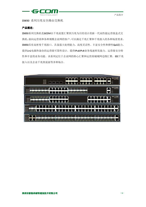
S5650 系列万兆安全路由交换机产品概述:S5650系列交换机是GCOM以千兆流量汇聚到万兆为目的设计的新一代高性能运营级盒式交换机,面向运营商和各种规模企业网的客户,可以满足千兆汇聚和千兆接入的各种场景需求。
S5650具有高密度千兆接口,具备强大处理能力,高度灵活性、丰富安全性和弹性QoS能力,提供1+1电源热备份的运营级可靠性设计,提供IPv4/IPv6业务线速转发能力、运营级安全特性和丰富的业务功能。
该系列定位于企业网的核心汇聚和运营商城域网边缘汇聚,IDC千兆接入以及企业千兆到桌面等多种场合。
产品特性:运营级的设备稳定性和网络弹性•采用在全球运营商网络中有大规模应用的NGBN自主知识产权操作系统•支持VRRP/GERP/MSTP/smartlink等多种链路冗余和网络冗余协议•支持1+1热拔插冗余电源完善的安全机制•采用基于硬件的逐包转发机制,可针对特征报文进行有效检测和过滤•支持基于MAC地址的ARP攻击自动防护和自动用户封杀功能•支持各种防DDoS、CPU过流保护和VRRP等设备保护功能•支持DHCP snooping/IP source Guard/802.1X/丰富的安全特性有效保障用户、设备和网络的可用性•支持BFD、FlexLink、动态链路汇聚和以太网环网等链路保护功能强大的QoS能力•支持双速三色2Rate3Color控制的流量管理策略•支持CAR实现基于端口和流的精确速率限制•支持各种流分类和QoS流控功能保障高优先级报文的传送•支持SP/WRR等各种优先级算法保障多媒体业务流的传输丰富的业务特性•支持静态、RIP、OSFP和BGP等单播路由协议•支持IGMP、PIM-DM、PIM-SM、PIM-SSM等组播路由协议•支持DHCP Server和DHCP Relay•支持L2-Tunneling透明封装网络边缘业务协议•支持Ethernet OAM协议丰富的IPv6特性•全面支持IPv6协议族及编址结构•支持IPv6静态路由、RIPng、OSFPv3、IS-ISv6、BGP4+等IPv6路由协议•支持丰富的IPv4向IPv6过渡技术,包括手工隧道、ISATAP隧道、6to4隧道等隧道技术•支持IPv6和IPv4双栈灵活的可扩展性•业务板插槽支持多种业务板,扩展更灵活•最大支持4个万兆端口,充分满足上行需要•支持堆叠功能,可通过10GE板卡进行堆叠☐背板带宽340Gbps☐包转发率147Mpps☐12个10/100/1000Base-T以太网端口☐12个光电复用端口(Combo口)☐2个万兆业务板插槽(2个(2*10GE))☐1+1冗余热备份电源☐支持堆叠☐满负荷功耗低于40W☐440mm(宽)*380mm(深)*44mm(高)S5650-28TM☐背板带宽340Gbps☐包转发率147Mpps☐12个100/1000Base-X SFP端口☐12个光电复用端口(Combo口)☐2个万兆业务板插槽(2个(2*10GE))☐1+1冗余热备份电源☐支持堆叠☐满负荷功耗低于50W☐440mm(宽)*380mm(深)*44mm(高)S5650-28SM☐背板带宽480Gbps☐包转发率190Mpps☐44个10/100/1000Base-T以太网端口☐4个光电复用端口(Combo口)☐2个万兆业务板插槽(2个(2*10GE))☐1+1冗余热备份电源☐支持堆叠☐满负荷功耗低于60W☐440mm(宽)*380mm(深)*44mm(高)S5650-52TMS5650-28PM☐背板带宽340Gbps☐包转发率147Mpps☐24个10/100/1000Base-T以太网端口☐4个光电复用端口(Combo口))☐2个万兆业务板插槽(2个(2*10GE))☐1+1冗余热备份电源☐支持堆叠☐主机满负荷功耗低于40W☐POE供电满足802.3af标准和802.3at标准☐单端口最大供电功率30W☐440mm(宽)*380mm(深)*44mm(高)☐产品规格:项目S5650-28TM S5650-28SM S5650-28PM S5650-52TM S5650-52SM 背板带宽340Gbps 640Gbps交换容量336Gbps 480Gbps包转发率(IPv4/IPv6)147Mpps 190Mpps内存和存储256MByte DDR2 SDRAM内存和8MB闪存冗余设计1+1电源冗余可插拔电源交流:输入90~260V,50~60Hz;功耗满载功耗≤40W空闲功耗≤15W满载功耗≤50W空闲功耗≤15W满载功耗≤40W空闲功耗≤15W满载功耗≤60W空闲功耗≤30W满载功耗≤70W空闲功耗≤30WPOE供电-- -- 单电源支持360W供电--- ---外形尺寸(宽*高*深) 440mm×380mm×44mm440mm×380mm×44mm440mm×380mm×44mm440mm×380mm×44mm440mm×380mm×44mm基本重量≤6kg ≤6kg ≤6kg ≤6.5kg ≤6.5kg环境参数运行温度:0°C~60°C存储温度:-40°C~70°C相对湿度:5%~95%,无凝结电磁兼容性业务特性:项目TiNet S5650系列二层特性MAC 支持静态、动态MAC表项支持16K个MAC地址支持黑洞MAC地址表(MAC Black Hole)支持端口MAC地址数量限制(Port MAC Limit)支持源MAC地址过滤☐背板带宽480Gbps☐包转发率190Mpps☐44个100/1000Base-X SFP端口☐4个光电复用端口(Combo口)☐2个万兆业务板插槽(2个(2*10GE))☐1+1冗余热备份电源☐支持堆叠☐满负荷功耗低于70W☐440mm(宽)*380mm(深)*44mm(高)S5650-52SM支持sticky MACVLAN 支持4K VLAN表项支持基于端口、MAC、协议和IP子网的VLAN支持1:1和N:1 VLAN Mapping功能支持端口QinQ和灵活QinQ(StackVLAN)支持Guest VLAN/Voice VLAN支持MUX VLAN支持LNP(链路类型协商协议)、Access、Trunk、Hybrid和QinQ接入方式支持VLAN Swap、VLAN Remark和VLAN Translate支持PVLAN实现端口隔离和节约公用VLAN资源支持基于以下策略的VLAN::MAC地址+IP地址,MAC地址+IP地址+端口支持GVRP支持default VLAN支持基于端口给报文添加双层VLAN tag生成树支持STP/RSTP/MSTP 支持远端环路检测端口支持双向带宽控制支持静态和LACP动态汇聚端口聚合支持端口和流镜像安全特性用户安全支持Anti-ARP-spoofing欺骗防护支持Anti-ARP-flooding泛洪攻击自动抑制支持IP Source Guard自动创建IP+MAC+端口+VLAN绑定表支持Port Isolation硬件隔离各端口间的报文支持MAC地址绑定到端口和端口MAC地址过滤支持IEEE 802.1x和AAA/Radiu/NAC的用户身份认证支持单端口最大用户数限制支持IEEE802.1x认证设备安全支持控制层上防止各种针对CPU的DOS攻击和病毒攻击支持SSHv2 Secure Shell支持SNMP v3加密管理支持Security IP的Telnet的登录和口令机制支持采用维护用户分级保护,防止未授权用户的非法侵入网络安全支持基于每用户MAC地址ARP流量检测支持基于ARP流量检测的ARP报文抑制或者用户封杀支持基于动态ARP表的一键绑定支持IP地址、VLAN ID、MAC地址和端口等参数的手工绑定支持自定义报文头部80字节深度的L2-L7 ACL流过滤支持端口广播/多播报文抑制和危险端口自动关闭支持ARP攻击的自动防御支持防止DOS、ARP、ICMP攻击功能支持广播风暴控制支持DHCP Snooping,防止私设DHCP服务器支持URPF单播反向路径检查,防止IP地址仿冒和攻击支持DHCP Option82和PPPoE+上传用户物理位置信息支持OSPF、RIPv2 及BGPv4 报文的明文及MD5密文认证IP路由IPv4支持ARP Proxy支持DHCP Relay支持DHCP Server支持静态路由支持RIP v1/v2支持OSPFv2/v3支持BGPv4支持等价路由支持策略路由支持路由策略支持MPLS-TE隧道建立支持全分布式的MPLS L3 VPN支持路由热备份技术支持跨设备的链路聚合支持VPLS支持MCEIPv6支持ICMPv6支持ICMPv6重定向支持DHCPv6支持ACLv6支持OSPF/OSPFv3支持RIPng支持BGP4+支持手工隧道支持ISATAP支持6to4隧道支持IPv6和IPv4双栈业务特性ACL支持标准和扩展ACL支持基于时间段(Time Range)ACL策略支持根据ACL进行流分类提供基于源/目的MAC地址、VLAN、802.1p、ToS、DiffServ、源/目的IP(IPv4/IPv6)地址、TCP/UDP端口号、协议类型等IP报文头信息的流分类和流定义支持L2~L7深入IP报文头部80字节的报文过滤QoS支持对端口或者自定义流的接收和发送报文的速率进行限速,并提供对自定义流的普通流量监管支持CAR(Committed Access Rate)、流量整形(Traffic Shapping)和流量统计支持对端口或者自定义流的报文镜像和报文重定向支持对端口或者自定义流的优先级标记,并提供802.1P、DSCP优先级的Remark能力支持基于端口或者自定义流的高级队列调度,每端口/流支持8个优先级队列,提供SP、WRR、SP+WRR等多种队列调度算法支持拥塞避免机制,包括Tail-Drop、WRED等功能组播支持IGMPv1/v2/v3支持IGMPv1/v2/v3 Snooping支持IGMP Filter组播过滤支持MVR组播VLAN注册和跨VLAN组播复制支持IGMP Fast leave快速离开组播组支持IGMP Proxy支持PIM-SM/PIM-DM/PIM-SSM支持PIM-SMv6、PIM-DMv6、PIM-SSMv6支持MLDv2/MLDv2 Snooping可靠特性环路保护支持EAPS和GERP增强以太网环网协议(环路愈合时间<50ms)支持Loopback-detection 端口环回检测链路保护支持FlexLink链路备份(链路愈合时间<50ms)支持RSTP/MSTP链路愈合硬件加速能力(环路愈合时间<1s) 支持LACP动态链路汇聚(链路愈合时间<10ms)支持BFD链路侦测设备保护支持VRRP主机备份支持主机程序和配置文件的双容错备份支持1+1电源热备份维护特性网络维护支持基于Telnet的端口实时流量、利用率和收发包统计支持RFC3176 sFlow流量分析,可以实现基于协议或地址的流量监控和统计支持LLDP邻居设备发现协议支持802.3ah Ethernet OAM支持数据日志和RFC 3164 BSD syslog Protocol支持Ping和Traceroute设备管理支持堆叠支持命令行接口(CLI)、Console口、Telnet和WEB配置管理支持SNMPv1/v2/v3支持RMON (Remote Monitoring)1,2,3,9组MIB支持NTP/SNTP网络时间协议支持SSH/Syslog支持GN.LinkⅡServer支持NGBNView网管系统订购信息:型号产品描述S5650-28TM 12*10/100/1000BaseT,12 Combo GE, 2*扩展槽, 1+1冗余电源扩展槽S5650-28SM 12*100/1000BaseX SFP,12 Combo GE,2*扩展槽,1+1冗余电源扩展槽S5650-28PM 24*10/100/1000BaseT,4 Combo GE, 2*扩展槽, 1+1冗余电源扩展槽S5650-52TM 44*10/100/1000BaseT,4 Combo GE, 4*10GE SFP+扩展槽, 1+1冗余电源扩展槽S5650-52SM 44*100/1000BaseX SFP,4 Combo GE, 4*10GE SFP+扩展槽,1+1冗余电源扩展槽SW2-10GE-1SFP 1*10GE SFP+ 单端口业务版(业务板,需要配SFP+模块使用)SW2-10GE-2SFP 2*10GE SFP+ 单端口业务版(业务板,需要配SFP+模块使用)NG01PWR100AC S5650-28TM/28SM ,100W交流220V电源模块NG01PWR180AC S5650-52TM/52SM ,180W交流220V电源模块NG01PWR100DC S5650-28TM/28SM ,100W直流-48V电源模块NG01PWR180DC S5650-52TM/52SM ,180W直流-48V电源模块。
AT28BV256-20中文资料

Features•Single 2.7V - 3.6V Supply•Fast Read Access Time – 200 ns •Automatic Page Write Operation –Internal Address and Data Latches for 64 Bytes –Internal Control Timer •Fast Write Cycle Times–Page Write Cycle Time: 10 ms Maximum –1- to 64-byte Page Write Operation •Low Power Dissipation –15 mA Active Current–20 µA CMOS Standby Current•Hardware and Software Data Protection •DATA Polling for End of Write Detection •High Reliability CMOS Technology –Endurance: 10,000 Cycles –Data Retention: 10 Years•JEDEC Approved Byte-wide Pinout•Commercial and Industrial Temperature RangesDescriptionThe A T28BV256 is a high-performance Electrically Erasable and Programmable Read Only Memory. Its 256K of memory is organized as 32,768 words by 8 bits. Manufac-tured with Atmel’s advanced nonvolatile CMOS technology, the device offers access times to 200 ns with power dissipation of just 54 mW. When the device is deselected, the CMOS standby current is less than 200 µA.PLCC – Top ViewPin ConfigurationsPin Name Function A0 - A14Addresses CE Chip Enable OE Output Enable WE Write Enable I/O0 - I/O7Data Inputs/Outputs NC No Connect DCDon’t ConnectPDIP , SOIC – Top ViewNote:1.Note: PLCC package pins 1 and 17are DON’T CONNECT.TSOP – Top View2AT28BV2560273H–PEEPR–10/04The AT28BV256 is accessed like a Static RAM for the read or write cycle without the need for external components. The device contains a 64-byte page register to allow writing of up to 64 bytes simultaneously. During a write cycle, the addresses and 1 to 64 bytes of data are inter-nally latched, freeing the address and data bus for other operations. Following the initiation of a write cycle, the device will automatically write the latched data using an internal control write cycle has been detected a new access for a read or w rite c an begin.Atmel’s AT28BV256 has additional features to ensure high quality and manufacturability. The device utilizes internal error correction for extended endurance and improved data retention characteristics. An optional software data protection mechanism is available to guard against inadvertent writes. The device also includes an extra 64 bytes of EEPROM for device identifi-cation or tracking.Block DiagramAbsolute Maximum Ratings*Temperature under Bias ................................-55°C to +125°C *NOTICE:Stresses beyond those listed under “Absolute Maximum Ratings” may cause permanent dam-age to the device. This is a stress rating only and functional operation of the device at these or any other conditions beyond those indicated in the operational sections of this specification is not implied. Exposure to absolute maximum rating conditions for extended periods may affect device reliabilityStorage Temperature.....................................-65°C to +150°C All Input Voltages (including NC Pins)with Respect to Ground...................................-0.6V to +6.25V All Output Voltageswith Respect to Ground.............................-0.6V to V CC + 0.6V Voltage on OE and A9with Respect to Ground...................................-0.6V to +13.5V3AT28BV2560273H–PEEPR–10/04Device OperationREAD:high, the data stored at the memory location determined by the address pins is asserted on This dual-line control gives designers flexibility in preventing bus contention in their system.BYTE WRITE:been started, it will automatically time itself to completion. Once a programming operation has been initiated and for the duration of t WC , a read operation will effectively be a polling operation.PAGE WRITE: The page write operation of the AT28BV256 allows 1 to 64 bytes of data to be written into the device during a single internal programming period. A page write operation is initiated in the same manner as a byte write; the first byte written can then be followed by 1 to 63 additional bytes. Each successive byte must be written within 150 µs (t BLC ) of the previous byte. If the t BLC limit is exceeded the AT28BV256 will cease accepting data and commence the internal programming operation. All bytes during a page write operation must reside on the during the page write operation, A6 - A14 must be the same.The A0 to A5 inputs are used to specify which bytes within the page are to be written. The bytes may be loaded in any order and may be altered within the same load period. Only bytes which are specified for writing will be written; unnecessary cycling of other bytes within the page does not occur.During a byte or page write cycle, an attempted read of the last byte written will result in the complement of the written data to be presented on I/O7. Once the write cycle has been com-begin at anytime during the write cycle.TOGGLE BIT:determining the end of a write cycle. During the write operation, successive attempts to read data from the device will result in I/O6 toggling between one and zero. Once the write has completed, I/O6 will stop toggling and valid data will be read. Reading the toggle bit may begin at any time during the write cycle.DATA PROTECTION: If precautions are not taken, inadvertent writes may occur during transi-tions of the host system power supply. Atmel has incorporated both hardware and software features that will protect the memory against inadvertent writes.HARDWARE PROTECTION: Hardware features protect against inadvertent writes to the AT28BV256 in the following ways: (a) V CC power-on delay – once V CC has reached 1.8V (typ-ical) the device will automatically time out 10 ms (typical) before allowing a write; (b) write SOFTWARE DATA PROTECTION: A software-controlled data protection feature has been implemented on the AT28BV256. Software data protection (SDP) helps prevent inadvertent writes from corrupting the data in the device. SDP can prevent inadvertent writes during power-up and power-down as well as any other potential periods of system instability.The AT28BV256 can only be written using the software data protection feature. A series of three write commands to specific addresses with specific data must be presented to the device before writing in the byte or page mode. The same three write commands must begin each write operation. All software write commands must obey the page mode write timing4AT28BV2560273H–PEEPR–10/04specifications. The data in the 3-byte command sequence is not written to the device; the address in the command sequence can be utilized just like any other location in the device.Any attempt to write to the device without the 3-byte sequence will start the internal write tim-ers. No data will be written to the device; however, for the duration of t WC , read operations will effectively be polling operations.DEVICE IDENTIFICATION: An extra 64 bytes of EEPROM memory are available to the user for device identification. By raising A9 to 12V ± 0.5V and using address locations 7FC0H to 7FFFH the additional bytes may be written to or read from in the same manner as the regular memory array.Notes:1.X can be V IL or V IH .2.Refer to AC programming waveforms.3.V H = 12.0V ± 0.5V .DC and AC Operating RangeAT28BV256-20AT28BV256-25Operating Temperature (Case)Com.0°C - 70°C 0°C - 70°C Ind.-40°C - 85°C -40°C - 85°C V CC Power Supply2.7V -3.6V2.7V -3.6VOperating ModesMode CE OE WE I/O Read V IL V IL V IH D OUT Write (2)V IL V IH V IL D IN Standby/Write Inhibit V IH X (1)X High ZWrite Inhibit X X V IH Write Inhibit X V IL X Output Disable X V IH X High Z Chip Erase V ILV H (3)V ILHigh Z DC CharacteristicsSymbol Parameter ConditionMinMax Units I LI Input Load Current V IN = 0V to V CC + 1V 10µA I LO Output Leakage Current V I/O = 0V to V CC10µA I SB V CC Standby Current CMOS CE = V CC - 0.3V to V CC + 1V Com.20µA Ind.50µA I CC V CC Active Current f = 5 MHz; I OUT = 0 mA15mA V IL Input Low Voltage 0.6V V IH Input High Voltage 2.0V V OL Output Low Voltage I OL = 1.6 mA 0.3V V OHOutput High VoltageI OH = -100 µA2.0V5AT28BV2560273H–PEEPR–10/04AC Read Waveforms (1)(2)(3)(4)Notes:1.ACC - t CE after the address transition without impact on t ACC .2.OE may be delayed up to t CE - t OE after the falling edge of CE without impact on t CE or by t ACC - t OE after an address changewithout impact on t ACC .3.t DF is specified from OE or CE whichever occurs first (C L = 5 pF).4.This parameter is characterized and is not 100% tested.AC Read CharacteristicsSymbol ParameterAT28BV256-20AT28BV256-25Units MinMax MinMax t ACC Address to Output Delay 200250ns t CE (1)CE to Output Delay 200250ns t OE (2)OE to Output Delay 0800100ns t DF (3)(4)CE or OE to Output Float055060ns t OHOutput Hold from OE, CE or Address, whichever occurred first00ns6AT28BV2560273H–PEEPR–10/04Input Test Waveforms and Measurement LevelOutput Test LoadNote:1.This parameter is characterized and is not 100% tested.R F Pin Capacitancef = 1 MHz, T = 25°C (1)Symbol Typ Max Units Conditions C IN 46pF V IN = 0V C OUT 812pFV OUT = 0V7AT28BV2560273H–PEEPR–10/04Note:1.NR = No Restriction.AC Write WaveformsWE ControlledCE ControlledAC Write CharacteristicsSymbol ParameterMin MaxUnits t AS , t OES Address, OE Set-up Time 0ns t AH Address Hold Time 50ns t CS Chip Select Set-up Time 0ns t CH Chip Select Hold Time 0ns t WP Write Pulse Width (WE or CE)200ns t DS Data Set-up Time 50ns t DH , t OEH Data, OE Hold Time 0nst DV Time to Data Valid NR(1)8AT28BV2560273H–PEEPR–10/04Programming Algorithm (1)(2)(3)Notes:1.Data Format: I/O7 - I/O0 (Hex); Address Format: A14 - A0 (Hex).2.Data protect state will be re-activated at the end of program cycle.3. 1 to 64 bytes of data are loaded.Software Protected Program Cycle Waveforms (1)(2)(3)Notes:1.A0 - A14 must conform to the addressing sequence for the first three bytes as shown above.2.A6 through A14 must specify the same page address during each high to low transition of WE (or CE) after the softwarecode has been entered.3.OE must be high only when WE and CE are both low.Page Mode CharacteristicsSymbol Parameter MinMax Units t WC Write Cycle Time 10ms t AS Address Set-up Time 0ns t AH Address Hold Time 50ns t DS Data Set-up Time 50ns t DH Data Hold Time 0ns t WP Write Pulse Width 200ns t BLC Byte Load Cycle Time 150µs t WPHWrite Pulse Width High100ns9AT28BV2560273H–PEEPR–10/04Notes:1.These parameters are characterized and not 100% tested.2.See “AC Read Characteristics” on page 5.Notes:1.These parameters are characterized and not 100% tested.2.See “AC Read Characteristics” on page 5.Toggle Bit WaveformsNotes:1.2.Beginning and ending state of I/O6 will vary.3.Any address location may be used but the address should not vary.(1)Symbol Parameter Min TypMaxUnits t DH Data Hold Time 0ns t OEH OE Hold Time 0ns t OE OE to Output Delay (2)ns t WR Write Recovery TimensToggle Bit Characteristics (1)Symbol Parameter Min TypMaxUnits t DH Data Hold Time 10ns t OEH OE Hold Time 10ns t OE OE to Output Delay (2)ns t OEHP OE High Pulse 150ns t WR Write Recovery Time0ns10AT28BV2560273H–PEEPR–10/0411AT28BV2560273H–PEEPR–10/04Note: 1.See Valid Part Numbers table below.Ordering Information (1)t ACC (ns)I CC (mA)Ordering Code Package Operation Range Active Standby 200150.02A T28BV256-20JC A T28BV256-20PC A T28BV256-20SC A T28BV256-20TC 32J 28P628S 28T Commercial (0° to 70°C)150.02A T28BV256-20JI A T28BV256-20PI A T28BV256-20SI A T28BV256-20TI 32J 28P628S 28T Industrial (-40° to 85°C)150.02A T28BV256-20TU A T28BV256-20JU 32J Green 28T Green Industrial (-40° to 85°C)250150.02A T28BV256-25JC A T28BV256-25PC A T28BV256-20SC A T28BV256-25TC 32J 28P628S 28T Commercial (0° to 70°C)150.02A T28BV256-25JI A T28BV256-25PI A T28BV256-20SI A T28BV256-25TI32J 28P628S 28TIndustrial (-40° to 85°C)Valid Part NumbersThe following table lists standard Atmel products that can be ordered.Device Numbers Speed Package and Temperature Combinations AT28BV25620JC, JI, PC, PI, SC, SI, TC, TI, TU, JU AT28BV25625JC, JI, PC, PI, SC, SI, TC, TIDie ProductsReference Section: Parallel EEPROM Die ProductsPackage Type32J 32-lead, Plastic J-leaded Chip Carrier (PLCC)28P628-lead, 0.600" Wide, Plastic Dual Inline Package (PDIP)28S 28-lead, 0.300" Wide, Plastic Gull Wing Small Outline (SOIC)28T28-lead, Plastic Thin Small Outline Package (TSOP)12AT28BV2560273H–PEEPR–10/04Packaging Information32J – PLCC13AT28BV2560273H–PEEPR–10/0428P6 – PDIP14AT28BV2560273H–PEEPR–10/0428S – SOIC15AT28BV2560273H–PEEPR–10/0428T – TSOP0273H–PEEPR–10/04Disclaimer: The information in this document is provided in connection with Atmel products. No license, express or implied, by estoppel or otherwise, to any intellectual property right is granted by this document or in connection with the sale of Atmel products. EXCEPT AS SET FORTH IN ATMEL’S TERMS AND CONDI-TIONS OF SALE LOCATED ON ATMEL’S WEB SITE, ATMEL ASSUMES NO LIABILITY WHATSOEVER AND DISCLAIMS ANY EXPRESS, IMPLIED OR STATUTORY WARRANTY RELATING TO ITS PRODUCTS INCLUDING, BUT NOT LIMITED TO, THE IMPLIED WARRANTY OF MERCHANTABILITY, FITNESS FOR A PARTICULAR PURPOSE, OR NON-INFRINGEMENT. IN NO EVENT SHALL ATMEL BE LIABLE FOR ANY DIRECT, INDIRECT, CONSEQUENTIAL, PUNITIVE, SPECIAL OR INCIDEN-TAL DAMAGES (INCLUDING, WITHOUT LIMITATION, DAMAGES FOR LOSS OF PROFITS, BUSINESS INTERRUPTION, OR LOSS OF INFORMATION) ARISING OUT OF THE USE OR INABIL ITY TO USE THIS DOCUMENT, EVEN IF ATMEL HAS BEEN ADVISED OF THE POSSIBIL ITY OF SUCH DAMAGES. Atmel makes no representations or warranties with respect to the accuracy or completeness of the contents of this document and reserves the right to make changes to specifications and product descriptions at any time without notice. Atmel does not make any commitment to update the information contained herein. Atmel’s products are not intended, authorized, or warranted for use as components in applications intended to support or sustain life.Atmel CorporationAtmel Operations2325 Orchard Parkway San Jose, CA 95131, USA Tel: 1(408) 441-0311Fax: 1(408) 487-2600Regional HeadquartersEuropeAtmel SarlRoute des Arsenaux 41Case Postale 80CH-1705 Fribourg SwitzerlandTel: (41) 26-426-5555Fax: (41) 26-426-5500AsiaRoom 1219Chinachem Golden Plaza 77 Mody Road Tsimshatsui East Kowloon Hong KongTel: (852) 2721-9778Fax: (852) 2722-1369Japan9F, Tonetsu Shinkawa Bldg.1-24-8 ShinkawaChuo-ku, Tokyo 104-0033JapanTel: (81) 3-3523-3551Fax: (81) 3-3523-7581Memory2325 Orchard Parkway San Jose, CA 95131, USA Tel: 1(408) 441-0311Fax: 1(408) 436-4314Microcontrollers2325 Orchard Parkway San Jose, CA 95131, USA Tel: 1(408) 441-0311Fax: 1(408) 436-4314La Chantrerie BP 7060244306 Nantes Cedex 3, France Tel: (33) 2-40-18-18-18Fax: (33) 2-40-18-19-60ASIC/ASSP/Smart CardsZone Industrielle13106 Rousset Cedex, France Tel: (33) 4-42-53-60-00Fax: (33) 4-42-53-60-011150 East Cheyenne Mtn. Blvd.Colorado Springs, CO 80906, USA Tel: 1(719) 576-3300Fax: 1(719) 540-1759Scottish Enterprise Technology Park Maxwell BuildingEast Kilbride G75 0QR, Scotland Tel: (44) 1355-803-000Fax: (44) 1355-242-743RF/AutomotiveTheresienstrasse 2Postfach 353574025 Heilbronn, Germany Tel: (49) 71-31-67-0Fax: (49) 71-31-67-23401150 East Cheyenne Mtn. Blvd.Colorado Springs, CO 80906, USA Tel: 1(719) 576-3300Fax: 1(719) 540-1759Biometrics/Imaging/Hi-Rel MPU/ High Speed Converters/RF DatacomAvenue de Rochepleine BP 12338521 Saint-Egreve Cedex, France Tel: (33) 4-76-58-30-00Fax: (33) 4-76-58-34-80Literature Requests/literature© Atmel Corporation 2004. All rights reserved. Atmel ®, logo and combinations thereof, are registered trademarks, and Everywhere You Are SM are the trademarks of Atmel Corporation or its subsidiaries. Other terms and product names may be trademarks of others.。
- 1、下载文档前请自行甄别文档内容的完整性,平台不提供额外的编辑、内容补充、找答案等附加服务。
- 2、"仅部分预览"的文档,不可在线预览部分如存在完整性等问题,可反馈申请退款(可完整预览的文档不适用该条件!)。
- 3、如文档侵犯您的权益,请联系客服反馈,我们会尽快为您处理(人工客服工作时间:9:00-18:30)。
1© 2005 by Catalyst Semiconductor, Inc.Characteristics subject to change without notices CMOS and TTL compatible I/O s Automatic page write operation:– 1 to 32 bytes in 5ms– Page load timers End of write detection:– Toggle bit – DATA polling – RDY/BUSYs Hardware and software write protection s 100,000 program/erase cycles s 100 year data retentionCAT28LV6564K-Bit CMOS PARALLEL EEPROM DESCRIPTIONThe CAT28LV65 is a low voltage, low power, CMOS parallel EEPROM organized as 8K x 8-bits. It requires a simple interface for in-system programming. On-chip address and data latches, self-timed write cycle with auto-clear and V CC power up/down write protection eliminate additional timing and protection hardware.DATA Polling, RDY/BUSY and Toggle status bit signal the start and end of the self-timed write cycle. Additionally,the CAT28LV65 features hardware and software write protection.The CAT28LV65 is manufactured using Catalyst’s advanced CMOS floating gate technology. It is designed to endure 100,000 program/erase cycles and has a data retention of 100 years. The device is available in JEDEC approved 28-pin DIP, 28-pin TSOP, 28-pin SOIC or 32-pin PLCC packages.BLOCK DIAGRAMFEATURESs 3.0V to 3.6V supply s Read access times:– 150/200/250nss Low power CMOS dissipation:– Active: 8 mA max.– Standby: 100 µA max.s Simple write operation:– On-chip address and data latches – Self-timed write cycle with auto-clears Fast write cycle time:– 5ms max.s Commercial, industrial and automotivetemperature rangesDoc. No. 1024, Rev. DA HAL O G E N F R E ETML EA D F R E ECAT28LV652Doc. No. 1024, Rev. DPIN CONFIGURATIONDIP Package (P, L)TSOP Top View (8mm x 13.4mm) (T13, H13)SOIC Package (J, W) (K, X)PLCC Package (N, G)OE A 9A 8NC WE V ccRDY/BUSYA 12A 7A 6A 5A 4A 3A 10CE I/07I/06I/05I/04I/03GND I/O 1I/O 0A 0A 1I/O 2A 2A 1112345678910111213142827262524232221201918171615PIN FUNCTIONSPin Name Function Pin Name Function A 0–A 12Address Inputs WE Write Enable I/O 0–I/O 7Data Inputs/Outputs V CC 3.0 to 3.6 V Supply CE Chip Enable V SS Ground OE Output Enable NCNo ConnectRDY/BSYReady/Busy StatusI/O 2V SSI/O 6I/O 5A 1A 0I/O 0I/O 1OE A 10CE I/O 7A 5A 4A 3A 2RDY/BUSYA 12A 7A 6A 9A 11V CC WE NC A 8I/O 4I/O 3A 6A 5A 4A 35678A 2A 1A 0NC 9101112I/O 013A 8A 9A 11NC 29282726OE A 10CE 25242322I/O 721I /O 1I /O 2V S S N CI /O 3I /O 4I /O 5141516171819204321323130A 7A 12R D Y /B U S Y NC V C CW E N CI/O 6TOP VIEW I/O 2V SSI/O 6I/O 5A 1A 0I/O 0I/O 1OE A 10I/O 7A 5A 4A 3A 2A 12A 7A 6A 9A 11V CC WE NC A 8I/O 4I/O 3RDY/BUSYCAT28LV653Doc. No. 1024, Rev. D*COMMENTStresses above those listed under “Absolute Maximum Ratings” may cause permanent damage to the device.These are stress ratings only, and functional operation of the device at these or any other conditions outside of those listed in the operational sections of this specifica-tion is not implied. Exposure to any absolute maximum rating for extended periods may affect device perfor-mance and reliability.ABSOLUTE MAXIMUM RATINGS*Temperature Under Bias .................–55°C to +125°C Storage Temperature.......................–65°C to +150°C Voltage on Any Pin withRespect to Ground (2)...........–2.0V to +V CC + 2.0V V CC with Respect to Ground ...............–2.0V to +7.0V Package Power DissipationCapability (Ta = 25°C)...................................1.0W Lead Soldering Temperature (10 secs)............300°C Output Short Circuit Current (3)........................100 mA RELIABILITY CHARACTERISTICS Symbol Parameter Min.Max.Units Test MethodN END (1)Endurance 105Cycles/Byte MIL-STD-883, Test Method 1033T DR (1)Data Retention 100Years MIL-STD-883, Test Method 1008V ZAP (1)ESD Susceptibility 2000Volts MIL-STD-883, Test Method 3015I LTH (1)(4)Latch-Up100mAJEDEC Standard 17Note:(1)This parameter is tested initially and after a design or process change that affects the parameter.(2)The minimum DC input voltage is –0.5V. During transitions, inputs may undershoot to –2.0V for periods of less than 20 ns. Maximum DCvoltage on output pins is V CC +0.5V, which may overshoot to V CC +2.0V for periods of less than 20 ns.(3)Output shorted for no more than one second. No more than one output shorted at a time.(4)Latch-up protection is provided for stresses up to 100mA on address and data pins from –1V to V CC +1V.MODE SELECTIONModeCE WE OE I/O Power ReadL HL D OUT ACTIVE Byte Write (WE Controlled)LH D IN ACTIVE Byte Write (CE Controlled)L H D IN ACTIVE Standby, and Write Inhibit H X X High-Z STANDBY Read and Write InhibitX H HHigh-ZACTIVECAPACITANCE T A = 25°C, f = 1.0 MHzSymbol TestMax.Units Conditions C I/O (1)Input/Output Capacitance 10pF V I/O = 0V C IN (1)Input Capacitance6pFV IN = 0VCAT28LV654Doc. No. 1024, Rev. DNote:(1)This parameter is tested initially and after a design or process change that affects the parameter.(2)Output floating (High-Z) is defined as the state when the external data line is no longer driven by the output buffer.(3)V IHC = V CC –0.3V to V CC +0.3V.D.C. OPERATING CHARACTERISTICS V cc = 3.0V to 3.6V, unless otherwise specified.LimitsSymbol ParameterMin.Typ.Max.Units Test Conditions I CC V CC Current (Operating, TTL)8mA CE = OE = V IL ,f = 1/t RC min, All I/O’s Open I SBC (3)V CC Current (Standby, CMOS)100µA CE = V IHC ,All I/O’s Open I LI Input Leakage Current –11µA V IN = GND to V CC I LO Output Leakage Current –55µA V OUT = GND to V CC ,CE = V IHV IH (3)High Level Input Voltage 2V CC +0.3V V IL Low Level Input Voltage –0.30.6V V OH High Level Output Voltage 2V I OH = –100µA V OL Low Level Output Voltage 0.3V I OL = 1.0mAV WIWrite Inhibit Voltage2V28LV65-1528LV65-20 28LV65-25 Symbol Parameter Min.Max.Min.Max.Min.Max.Units t RC Read Cycle Time 150200250ns t CE CE Access Time 150200250ns t AA Address Access Time 150200250ns t OE OE Access Time 7080100ns t LZ (1)CE Low to Active Output 000ns t OLZ (1)OE Low to Active Output 0ns t HZ (1)(2)CE High to High-Z Output 505055ns t OHZ (1)(2)OE High to High-Z Output 505055ns Output Hold from t OH (1)Address Change00nsA.C. CHARACTERISTICS, Read Cycle V cc = 3.0V to 3.6V, unless otherwise specified.CAT28LV655Doc. No. 1024, Rev. DC L INCLUDES JIG CAPACITANCEL = 100 pFINPUT PULSE LEVELSREFERENCE POINTS2.0 V0.6 V V - 0.3 V 0.0 VCCFigure 1. A.C. Testing Input/Output Waveform (4)Figure 2. A.C. Testing Load Circuit (example)Note:(1)This parameter is tested initially and after a design or process change that affects the parameter.(2) A write pulse of less than 20ns duration will not initiate a write cycle.(3) A timer of duration t BLC max. begins with every LOW to HIGH transition of WE . If allowed to time out, a page or byte write will begin;however a transition from HIGH to LOW within t BLC max. stops the timer.(4)Input rise and fall times (10% and 90%) < 10 ns.28LV65-1528LV65-2028LV65-25Symbol Parameter MinMax MinMax MinMax Units t WC Write Cycle Time 555ms t AS Address Setup Time0000ns t AH Address Hold Time 100100100ns t CS CE Setup Time 000ns t CH CE Hold Time 000ns t CW (2)CE Pulse Time 110150150ns t OES OE Setup Time 01010ns t OEH OE Hold Time 01010ns t WP (2)WE Pulse Width 110150150ns t DS Data Setup Time 60100100ns t DH Data Hold Time 000ns t INIT (1)Write Inhibit Period After Power-up 510510510ms t BLC (1)(3)Byte Load Cycle Time 0.051000.11000.1100µs t RBWE Low to RDY/Bus y Low220220220nsA.C. CHARACTERISTICS, Write Cycle V cc = 3.0V to 3.6V, unless otherwise specified.CAT28LV656Doc. No. 1024, Rev. DByte WriteA write cycle is executed when both CE and WE are low,and OE is high. Write cycles can be initiated using either WE or CE , with the address input being latched on the falling edge of WE or CE , whichever occurs last. Data,conversely, is latched on the rising edge of WE or CE ,whichever occurs first. Once initiated, a byte write cycle automatically erases the addressed byte and the new data is written within 5 ms.DEVICE OPERATIONReadData stored in the CAT28LV65 is transferred to the data bus when WE is held high, and both OE and CE are held low. The data bus is set to a high impedance state when either CE or OE goes high. This 2-line control architec-ture can be used to eliminate bus contention in a system environment.CAT28LV657Doc. No. 1024, Rev. DPage WriteThe page write mode of the CAT28LV65 (essentially an extended BYTE WRITE mode) allows from 1 to 32 bytes of data to be programmed within a single EEPROM write cycle. This effectively reduces the byte-write time by a factor of 32.Following an initial WRITE operation (WE pulsed low, for t WP , and then high) the page write mode can begin by issuing sequential WE pulses, which load the address and data bytes into a 32 byte temporary buffer. The page address where data is to be written, specified by bits A 5to A 12, is latched on the last falling edge of WE . Each byte within the page is defined by address bits A 0 to A 4(which can be loaded in any order) during the first and subsequent write cycles. Each successive byte load cycle must begin within t BLC MAX of the rising edge of the preceding WE pulse. There is no page write window limitation as long as WE is pulsed low within t BLC MAX .Upon completion of the page write sequence, WE must stay high a minimum of t BLC MAX for the internal auto-matic program cycle to commence. This programming cycle consists of an erase cycle, which erases any data that existed in each addressed cell, and a write cycle,which writes new data back into the cell. A page write will only write data to the locations that were addressed and will not rewrite the entire page.BYTE 0BYTE 1BYTE 2BYTE nBYTE n+1BYTE n+2Figure 5. Byte Write Cycle [CE Controlled]CAT28LV658Doc. No. 1024, Rev. DWECEOEI/O 6DATA PollingDATA polling is provided to indicate the completion of write cycle. Once a byte write or page write cycle is initiated, attempting to read the last byte written will output the complement of that data on I/O 7 (I/O 0–I/O 6are indeterminate) until the programming cycle is com-plete. Upon completion of the self-timed write cycle, all I/O’s will output true data during a read cycle.Toggle BitIn addition to the DATA Polling feature, the device offers an additional method for determining the completion of a write cycle. While a write cycle is in progress, readingdata from the device will result in I/O 6 toggling between one and zero. However, once the write is complete, I/O 6stops toggling and valid data can be read from the device.Ready/BUSY (RDY/BUSY )The RDY/BUSY pin is an open drain output which indicates device status during programming. It is pulled low during the write cycle and released at the end of programming. Several devices may be OR-tied to the same RDY/BUSY line.Figure 7. DATA PollingFigure 8. Toggle BitNote:(1)Beginning and ending state of I/O 6 is indeterminate.CAT28LV659Doc. No. 1024, Rev. DHARDWARE DATA PROTECTIONThe following is a list of hardware data protection fea-tures that are incorporated into the CAT28LV65.(1)V CC sense provides for write protection when V CCfalls below 2.0V min.(2) A power on delay mechanism, t INIT (see AC charac-teristics), provides a 5 to 10 ms delay before a write sequence, after V CC has reached 2.40V min.(3)Write inhibit is activated by holding any one of OElow, CE high or WE high.(4)Noise pulses of less than 20 ns on the WE or CEinputs will not result in a write cycle.SOFTWARE DATA PROTECTIONThe CAT28LV65 features a software controlled data protection scheme which, once enabled, requires a data algorithm to be issued to the device before a write can be performed. The device is shipped from Catalyst with the software protection NOT ENABLED (the CAT28LV65 is in the standard operating mode).Figure 9.Write Sequence for Activating SoftwareData ProtectionFigure 10.Write Sequence for DeactivatingSoftware Data ProtectionSOFTWARE DATAPROTECTION ACTIVATED(12)Note:(1)Write protection is activated at this point whether or not any more writes are completed. Writing to addresses must occur within t BLCMax., after SDP activation.(1)CAT28LV6510Doc. No. 1024, Rev. DTo activate the software data protection, the device must be sent three write commands to specific addresses with specific data (Figure 9). This sequence of commands (along with subsequent writes) must adhere to the page write timing specifications (Figure 11). Once this is done,all subsequent byte or page writes to the device must be preceded by this same set of write commands. The data protection mechanism is activated until a deactivate sequence is issued regardless of power on/off transi-tions. This gives the user added inadvertent write pro-tection on power-up in addition to the hardware protec-tion provided.To allow the user the ability to program the device with an EEPROM programmer (or for testing purposes) there is a software command sequence for deactivating the data protection. The six step algorithm (Figure 10) will reset the internal protection circuitry, and the device will return to standard operating mode (Figure 12 provides reset timing). After the sixth byte of this reset sequence has been issued, standard byte or page writing can commence.Figure 11. Software Data Protection TimingFigure 12. Resetting Software Data Protection TimingCAT28LV6511Doc. No. 1024, Rev. DORDERING INFORMATIONNotes:(1)The device used in the above example is a CAT28LV65NI-25T (PLCC, Industrial temperature, 250 ns Access Time, Tape & Reel).* -40˚C to +125˚C is available upon requestCatalyst Semiconductor, Inc.Corporate Headquarters1250 Borregas AvenueSunnyvale, CA 94089Phone: 408.542.1000Fax: 408.542.1200 Copyrights, Trademarks and PatentsTrademarks and registered trademarks of Catalyst Semiconductor include each of the following:DPP ™AE 2 ™Catalyst Semiconductor has been issued U.S. and foreign patents and has patent applications pending that protect its products. For a complete list of patents issued to Catalyst Semiconductor contact the Company’s corporate office at 408.542.1000.CATALYST SEMICONDUCTOR MAKES NO WARRANTY, REPRESENTATION OR GUARANTEE, EXPRESS OR IMPLIED, REGARDING THE SUITABILITY OF ITS PRODUCTS FOR ANY PARTICULAR PURPOSE, NOR THAT THE USE OF ITS PRODUCTS WILL NOT INFRINGE ITS INTELLECTUAL PROPERTY RIGHTS OR THE RIGHTS OF THIRD PARTIES WITH RESPECT TO ANY PARTICULAR USE OR APPLICATION AND SPECIFICALLY DISCLAIMS ANY AND ALL LIABILITY ARISING OUT OF ANY SUCH USE OR APPLICATION, INCLUDING BUT NOT LIMITED TO, CONSEQUENTIAL OR INCIDENTAL DAMAGES.Catalyst Semiconductor products are not designed, intended, or authorized for use as components in systems intended for surgical implant into the body, or other applications intended to support or sustain life, or for any other application in which the failure of the Catalyst Semiconductor product could create a situation where personal injury or death may occur.Catalyst Semiconductor reserves the right to make changes to or discontinue any product or service described herein without notice. Products with data sheets labeled "Advance Information" or "Preliminary" and other products described herein may not be in production or offered for sale.Catalyst Semiconductor advises customers to obtain the current version of the relevant product information before placing orders. Circuit diagrams illustrate typical semiconductor applications and may not be complete.Publication #:1024Revison:D Issue date:03/29/05REVISION HISTORY et a D n o i s i v e R s t n e m m o C 40/92/30B s a e r a l l a n i s e g a k c a p n e e r G d e d d A 40/02/40C no i t a n g i s e d t e e h s a t a d e t e l e D no i t a m r o f n I g n i r e d r O e t a d p U yr o t s i H n o i s i v e R e t a d p U re b m u N v e R e t a d p U 50/92/30D el c y C e t i r W ,s c i t s i r e t c a r a h C C .A e t a d p U。