MH8S64AQFC-8中文资料
HMS12864F8VL资料

GENERAL DESCRIPTIONThe HMS12864F8VL is a high-speed static random access memory (SRAM) module containing 131,072 words organized in a x 64-bit configuration. The module consists of eight 128K x 8 SRAMs mounted on a 120-pin, both-sided, FR4-printed circuit board.Byte write enable inputs,(/WE0,/WE1,/WE2,/WE3,/WE4,/WE5,/WE6,/WE7) are used to enable the module ’s 8 bits independently. Output enable(/OE) and write enable(/WE) can set the memory input and output.Data is written into the SRAM memory when write enable (/WE) and chip enable (/CE) inputs are both LOW. Reading is accomplished when /WE remains HIGH and /CE and output enable (/OE) are LOW.For reliability, this SRAM module is designed as multiple power and ground pin. All module components may be powered from a single +3.3V DC power supply and all inputs and outputs are fully TTL-compatible.FEATURESP1 P2 PIN Symbol PIN Symbol PIN Symbol PIN Symbol1 Vcc 31 Vss 1 Vcc 31 Vss2 DQ32 32 DQ7 2 DQ24 32 DQ63 3 DQ33 33 DQ6 3 DQ25 33 DQ624 DQ34 34 DQ5 4 DQ26 34 DQ61 5 DQ35 35 DQ4 5 DQ27 35 DQ60 6 DQ36 36 DQ3 6 DQ28 36 DQ59 7 DQ37 37 DQ2 7 DQ29 37 DQ58 8 DQ38 38 DQ1 8 DQ30 38 DQ57 9 DQ39 39 DQ0 9 DQ31 39 DQ56 10 Vcc 40 Vss 10 Vcc 40 Vss 11 DQ40 41 DQ15 11 DQ16 41 DQ55 12 DQ41 42 DQ14 12 DQ17 42 DQ54 13 DQ42 43 DQ13 13 DQ18 43 DQ53 14 DQ43 44 DQ12 14 DQ19 44 DQ52 15 DQ44 45 DQ11 15 DQ20 45 DQ51 16 DQ45 46 DQ10 16 DQ21 46 DQ50 17 DQ46 47 DQ9 17 DQ22 47 DQ49 18 DQ47 48 DQ8 18 DQ23 48 DQ48 19 Vcc 49 Vss 19 Vcc 49 Vss 20 /WE0 50 A0 20 A16 50 NC 21 /WE1 51 A1 21 A15 51 NC 22 /WE2 52 A2 22 A14 52 /OE 23 /WE3 53 A3 23 A13 53 NC 24 /WE4 54 A4 24 A12 54 NC 25 Vcc 55 Vss 25 Vcc 55 Vss 26 /WE5 56 A5 26 A11 56 NC 27 /WE6 57 A6 27 A10 57 NC 28 /WE7 58 A7 28 A9 58 NC 29 /CS2 59 /CS1 29 A8 59 NC PIN ASSIGNMENTw Access times : 70 and 100ns w High-density 1MByte design w High-reliability, high-speed design w Single + 3.3V ±0.3V power supply w Easy memory expansion with /CE and /OE functionsw All inputs and outputs are TTL-compatible w Industry-standard pin-out w FR4-PCB designOPTIONS MARKINGw Timing70ns access - 70 100ns access -100w Packages120-pin SMM FFUNCTIONAL BLOCK DIAGRAMDQ0 – DQ63A0 - A16/WE0/WE1/WE2/CE/OE/WE3ABSOLUTE MAXIMUM RATINGSPARAMETER SYMBOL RATINGVoltage on Any Pin Relative to Vss V IN,OUT-0.5V to Vcc+0.5VVoltage on Vcc Supply Relative to Vss V CC-0.3V to 4.6VPower Dissipation P D8.0WStorage Temperature T STG-65o C to +150o COperating Temperature T A0o C to +70o Cw Stresses greater than those listed under " Absolute Maximum Ratings" may cause permanent damage to the device.This is a stress rating only and functional operation of the device at these or any other conditions above those indicated in the operating section of this specification is not implied. Exposure to absolute maximum rating conditions forextended periods may affect reliability.RECOMMENDED DC OPERATING CONDITIONS ( T A=0 to 70 o C )PARAMETER SYMBOL MIN TYP. MAX Supply Voltage V CC 3.0V 3.3V 3.6V Ground V SS0 0 0Input High Voltage V IH 2.2 - Vcc+0.3V** Input Low Voltage V IL-0.3* - 0.6V* V IL(Min.) = -2.0V ac (Pulse Width ≤ 10ns) for I ≤ 20 mA** V IH(Min.) = Vcc+2.0V ac (Pulse Width ≤ 10ns) for I ≤ 20 mADC AND OPERATING CHARACTERISTICS (1)(0o C ≤ T A ≤ 70 o C ; Vcc = 3.3V ± 10% ) PARAMETER TEST CONDITIONS SYMBOL MIN MAX UNITS Input Leakage Current VIN=Vss to Vcc IL I-8 8 µAOutput Leakage Current /CE=V IH or /OE =V IH or /WE=V ILV OUT=Vss to V CCIL0-8 8 µAOutput High Voltage I OH = -4.0Ma V OH 2.4 V Output Low Voltage I OL = 8.0mA V OL0.4 V * Vcc=3.3V, Temp=25 o CDC AND OPERATING CHARACTERISTICS (2)MAXDESCRIPTION TEST CONDITIONS SYMBOL70 100UNITPower Supply Current:Operating Min. Cycle, 100% Duty/CE=V IL, V IN=V IH or V IL,I OUT=0mAI CC32 32 mA Min. Cycle, /CE=V IH I SB 2.4 2.4 mAPower SupplyCurrent:Standbyf=0MHZ, /CE≥V CC-0.2V,V IN≥ V CC-0.2V or V IN≤0.2VI SB180 80 uACAPACITANCE (T A =25 o C , f= 1.0Mhz)DESCRIPTIONTEST CONDITIONSSYMBOL MAX UNIT Input /Output Capacitance V I/O =0VC I/O 80 pF Input CapacitanceV IN =0VC IN64pF* NOTE : Capacitance is sampled and not 100% testedAC CHARACTERISTICS (0o C ≤ T A ≤ 70 o C ; Vcc = 3.3V ± 0.3V, unless otherwise specified) Test conditionsPARAMETERVALUE Input Pulse Level 0.4V to 2.2VInput Rise and Fall Time5ns Input and Output Timing Reference Levels 1.5V Output Load See belowREAD CYCLE70100PARAMETERSYMBOLMINMAX MIN MAXUNITRead Cycle Time t RC 70 100 ns Address Access Time t AA 70 100ns Chip Select to Output t CO 70 100 ns Output Enable to Output t OE 35 50 ns Output Enable to Low-Z Output t OLZ 5 5 ns Chip Enable to Low-Z Output t LZ 10 10 ns Output Disable to High-Z Output t OHZ 0 25 0 30 ns Chip Disable to High-Z Output t HZ 0 25 0 30 ns Output Hold from Address Change t OH 10 15 ns Chip Select to Power Up Time t PU ns Chip Select to Power Down Time t PDns319Ω 5pF *D OUTOutput Load (B)for t HZ , t LZ , t WHZ , t OW , t OLZ & t OHZ50Ω30pFD OUTOutput Load (A)WRITE CYCLE70 100PARAMETER SYMBOLMIN MAX MIN MAXUNITWrite Cycle Time t WC70 100nsChip Select to End of Write t CW60 80 ns Address Set-up Time t AS0 0 ns Address Valid to End of Write t AW60 80 ns Write Pulse Width t WP55 70 ns Write Recovery Time t WR0 0 ns Write to Output High-Z t WHZ0 25 0 30 ns Data to Write Time Overlap t DW30 40 ns Data Hold from Write Time t DH0 0 ns End of Write to Output Low-Z t OW 5 5 nsTIMING DIAGRAMSTIMING WAVEFORM OF READ CYCLE(Address Controlled) ( /CE =/ OE = V IL , /WE = V IH) AddressData outTIMING WAVEFORM OF READ CYCLE ( /CE Controlled )Notes (Read Cycle) 1. /WE is high for read cycle.2. All read cycle timing is referenced from the last valid address to first transition address.3. t HZ and t OHZ are defined as the time at which the outputs achieve the open circuit condition and are not referenced to V OHor V OL levels.4. At any given temperature and voltage condition, t HZ (max.) is less than t LZ (min.) both for a given device and from device to device.5. Transition is measured ± 200mV from steady state voltage with Load (B). This parameter is sampled and not 100% tested.6. Device is continuously selected with /CE = V IL .7. Address valid prior to coincident with /CE transition low.TIMING WAVEFORM OF WRITE CYCLE (/OE=Clock )Address/CE/OEData OutVcc SupplyCurrentTIMING WAVEFORM OF WRITE CYCLE ( /OE Low Fixed )Notes (Write Cycle)1. All write cycle timing is referenced from the last valid address to the first transition address.2. A write occurs during the overlap of a low /CE and a low /WE. A write begins at the latest transition among /CE going low and /WE going low: A write ends at the earliest transition among /CE going high and /WE going high. t WP is measured from the beginning of write to the end of write.3. t CW is measured from the later of /CE going low to the end of write.4. t AS is measured from the address valid to the beginning of write.5. t WR is measured from the end of write to the address change. t WR applied in case a write ends as /CE, or /WE going high.6. If /OE,/CE and /WE are in the read mode during this period, the I/O pins are in the output low-Z state. Inputs of opposite phase of the output must not be applied because bus contention can occur.7. For common I/O applications, minimization or elimination of bus contention conditions is necessary during read and write cycle.8. If /CE goes low simultaneously with /WE going low or after /WE going low, the outputs remain high impedance state. 9. D OUT is the read data of the new address.10. When /CE is low : I/O pins are in the output state. The input signals in the opposite phase leading to the output should not be applied.FUNCTIONAL DESCRIPTION/CE /WE /OE MODE I/O PIN SUPPLY CURRENTH X* X Not Select High-Z l SB , l SB1 L H H Output DisableHigh-Z l CC L H L Read D OUT l CC LLXWriteD INl CCNote : X means Don't CareAddress/CE/WEData InData OutPACKAGING INFORMATIONFRONT SIDEREAR SIDEORDERING INFORMATIONPart Number Density Org. Package ComponentNumberVcc SPEEDHMS12864F8VL-70 1MByte X 64120 Pin-SMM8EA 3.3V 70ns HMS12864F8VL-100 1MByte X 64 120 Pin-SMM8EA 3.3V 100ns。
档案馆智能密集架控制系统及参数要求

融安特智能密集架技术参数要求编辑:融安特刘重庆一、产品名称:智能型密集架二、用途盛放标准的档案盒每1000平米不少于80万卷。
(具体情况需现场测量具体沟通)3. 喷塑表面色泽一致,塑面均匀光滑,无划伤。
4. 产品各零件、组合件之间应能具有互换性。
5. 传动机构应转动灵活、平稳、无失灵现象。
四、制造公差1. 每标准节组装后,外廓尺寸(长、宽、高)的极限偏差为±2mm。
2. 每标准节组装后,侧面板和中腰带的对缝处的间隙应小于2mm。
3. 门缝间隙均匀一致,并在1~2mm之间。
4. 轨道安装后,在任意1m长度内水平度偏差不大于1mm,全长不大于4mm,轨道之间对应点的水平偏差为1mm,每两条轨道之间的平行度偏差为1.5mm。
5. 立柱与导轨的垂直度不大于1.5mm。
6. 底梁必须平直,直线度不大于0.5mm/m,全长不大于2mm。
7. 架体安装垂直度偏差小于2mm,达到横平竖直。
五、智能档案密集架具体要求:1、架体技术要求:设备名称设备配置材料规格采用标准参考品牌性能说明轨道轨道座3.0mm热轧钢板GB699-88 宝钢、武钢表面静电喷塑或镀铬处理,喷塑前经严格去油除锈和磷化处理(下同)轨道20×25mm;45#实心方钢(镀硬铬处理)GB699-88 宝钢、武钢底盘底梁、轴承档、夹紧块3.0mm热轧钢板GB699-88 宝钢、武钢底盘采用整体焊接,刚性足,不变形,表面喷塑。
架体立柱1.5mm冷轧钢板GB710-88 宝钢、武钢架体结实、坚固、设计新颖,安装规范,层数和间距自由调整,表面喷塑平正光亮,色泽均匀一致,无鼓泡、脱落、伤痕等缺陷。
外观漂亮。
层板承重≤80kg,满负荷24小时后屈侥度≥3mm,制裁后自动恢复。
搁板1.2mm冷轧钢板GB710-88 宝钢、武钢挂板1.2mm冷轧钢板GB710-88 宝钢、武钢顶板1.0mm冷轧钢板GB710-88 宝钢、武钢护板1.0mm冷轧钢板GB710-88 宝钢、武钢门面门框1.0mm冷轧钢板GB710-88 宝钢、武钢门面平整,款式新颖,表面喷塑,ISO9001认证产品。
myslot

myslot公会宗旨:以义为先,以情为首,以实力证明,团结友爱齐心打造最特色的第一大混子公会!!!公会成员必须遵守的准则:1、禁止在YY上和Q群上乱发东西和吵架、骂人等等。
2、个人在游戏上和其他混子发生矛盾必须找流氓处理。
3、公会的混子不能骗自己公会的混子,欺骗公会混子的点卡或金钱等等。
4、公会的混子必须要听从流氓的命令。
任何公会任何家族和个体加盟我们《混子大队》公会,只要您有能力您有时间完全可以成为我们公会内阁混子参与公会发展大小事物的讨论.我们期待您的加盟加入共同发展我们公会#showtooltip 冰枪术/cancelaura 寒冰屏障/cast 冰枪术#showtooltip 法术反制/cancelaura 寒冰屏障/stopcasting/clearfocus [target=focus,dead]/clearfocus [target=focus,noexists]/Cast [target=focus,exists] 法术反制;法术反制#showtooltip 冰冷血脉/cast 生命之血/use 灾变角斗士的统御徽章/cast 冰冷血脉#showtooltip 寒冰箭/cancelaura 寒冰屏障/cast 寒冰箭@ Myslot 导出数据 ( V11)@ 时间:06/23/12 11:16:43@ 人物:Tamuura@ 职业:法师@ 天赋:奥术:2 火焰:8 冰霜:31@ 等级:85@@ 问题/建议请联系********************@ --------------------C1YEFupbt+0D4FYOAAGVWqCUBwqZAJILUpUNkKoPUDACBCdUpawQ1QspyQx EuAFI7RCIHwQVQyjBEUHVEqmiJ4JiCqTiCkGpLSDqixRhDEGKMwSV1hCR3h AE5hBR3SEo2ENQ4o8UySCqQ4JoEUg9ElKTCJK6RETZpKqqT1KCURJ1SqFWK ZV6JZWYJeCWFFW7VNAvgGFKJccUsEyoPJMSmaaq0jUp0DZA9I1QMk4QzoHI OhB6pyLzpCL3KGkfofBPCjFQUDlIYqGCHpI0UZIuimwUwkdIRqqok1C1kpD iJRQ1E0rdhIqdSP1EGCokRwlJLQX1lEhTIa5KaiuUfBUoYwHFWSlVa6VIvV Uq5hJSuqsCewkS/aXUYCmpw4oWC5LHSCar0GWgzZL4LBSjVcVplawmJHpNi Zotym2otJuU36oMl8hxgirLJTwnajrFdQLbKRHfhdJ4ITqvVLVeitJ7QGk+ Iar7Uqn2A5L/hKIBA+lAICyYongwRWVCEepCQUobEulDodSIQelEFFpRqPR iStSMQsWNqVI7ClV+LFWGFFR1pAhaUgk9GaSmFIErU0pbVlX5MiU0phC0Zq rwpiBozqpyJ1Ipe6aI/kypDJoKDkWRRYUoj6aSJhUhlwLVpylUoyqROjUFt Woq9GoKMitSqW4VEnYNVL8iZdiq5NiqVMumSp5NpUwrVHUtEdG2IuLbFNK4RJTOFSLWFQLvphTzplDurarYNxX1bwrYmIjiYyHJyERUTkYqsTIRqZeFVGY WUnUzEWFnQcTPgpKGFqRytKCopYWQp4VQUwsKXS2IsrUgydeCkLGFSGcLQq 0tiPS2EsnhgoTJBVFdLtXmRH0eqkZPVZ1eoNcFqTqeiKrpBUW+JyLZH6mk/ 0sGoMbQ5oYceuTuDCla/rxY815mrpKT//z6MYmTA2TzStOYSVnOAdSUje9o TzZTo0CIAwfkP79+TOLk24Y7cncmAwqB5lfF8TLOE2gGPJbHbj6g5tVLxn0 CzZTHXoBGUGgOake/Ko6XI7L9GSoDlQKc5bFP7ejaM15GgSbYpRmwiCmmXA o2L4NcuGB5bLVqV+ZTOzoKNE0/DUTASFMeW63QOim6k1sGThbJP+ixmw+oO a4V2LjAwN/uDmYy6LhWYOMCA38DA0AG4nYF4uICcS0F4v4G4oAMxIkViAvR 3UHt6OrMMvXhlqZ2Pa0MjUPUNAIdwN0ppnZ8uOVo3PHBOB+xPXJ3bhctf16 seS8zVykHyFRxlYxnj5qZGysKNEgxKcuXFoOAkUZQgOXx6aq48akdXTZF5d KOZRNw6IjsxYIF9NjNB9RcnbKRlsAsG+7TExcsQ+tobcgYO8e3ayAeY8PQ4 xOYyaCrUzbSEphlw3164oJlaB2tDRlj5/7eGPt7o0GPT6B2POVQUCGh3N0Z AyCCUGtp3gc5NJS7OwsbEC+EwckdxPb45trpIrM0ucUOg79fjh5yaCh3d5Y UQGUXZdlTpCmmQpnraUOBMU8byDFASYje3d2d0RVQCDTPHjUzN9O66+SVV3 ikdSAAyY/Ps0fNzCkrCjS0AFcpzFWZlJGH+/CkwHLk+OTZo2bm07rr5JVX+ L51IED58Xn2qJm5scpgBlKmDCngKNAohbkqkzJ4rfKG+/CkwHJkwPfH45NP 6+xiTqB29OxRM/NCs6JAoxTUZ4IvezH78KRAvFZ55cjxya9KmRJjYOzmA2p eKi7NlAvt8BAaokMfHs7xyc20mtllnhzUjg5qRy8Vl2bK0MgzM4Po0IeHZo 5POQSo4Ojd3d1ZUgCVXZRlT5GmmAplrqcNBcY8bSD/dgMJwd3d3Z0xACIIt ZbmORRmC+7u7u7u7u7uLGG0/Hmx5r3MXCUf7CqejrFjDpDNK1FTNpcWkwOo DJxF5VEC2XfMLGJAY608SiAHjuA8HngOoDJwFpVHCWTfMbOIAY218iiBHNA eGHnJRj7wHKBO2fiOmUUMaKyVRwnkABh5yUY+8MGu4ukYO54Gu4qnY+yYt4 Ic2oK7u7u7u7u7O7eOlj8v1ryXmavk5D3xyeJKlAOoqVFgNgXFdD1sw3rY5 ga7ikfuIX4OoKZsfFCEvfTOmPTGGyAHBSIHUFM2vmNmEQMaq3sNmjf354GT 98QniytRTuKuQhhG2DhPoBn+BghVwX0CzeRA36HQ6+gm/MGOEjLQAHhqx4e L8wSayYNADo2+P/iX/qcthwIUAs2zR83MK251tQCnASOKiQuWoSvFxAWhA9 qVBbzGR80C1Mz45BWIUtBIqeIqmTI0odWl4zQgdMDVhxtqGuwXo2bgLJJmi guUx7lkm4g2d46Ilj8v1ryXmavkOnDg5B+aTtpLF7tNDqCmRoHZFBTTdTSL OumX/n1vsMcvB1BTNq4DB07+oemkvXSx2+T/R81u7hwuWv68WPNeZq6S66R f5CY7kn9oOYCaGgVmU1BM19Es6qRf+ve9wR6/HEBN2bhO+kVusiP5h5a3AD n0yN25wWj582LNe5m5Sq4DB07+oemNiUAX518OEMigD/zNAdSUjevAgZN/aHpjItDF+ZeXR2JDubtzY9Hy58Wa9zJzlZzcrS35h6bv9dbDSpIDqKlRYDYF xXQdzaJO+qV/3xvs8csBsnklasrm0mJyAJWBs6g8SiD7jplFDGislUcJ5MA RnMcDzwFUBs6i8iiB7DtmFjGgsVYeJZAD2gMjL9nIB54D1Ckb3zGziAGNtf IogRwAIy/ZyAdO7taW/EPT93rrYSU5kbu1Jf/Q9L3eelhJ8vHIQLm78zFa/ rxY815mrpLrpF86aaP9mIL2S4wxB1BTNh4vQTtdwj9CLpKW+zEFzQECGfR4 IDrreyLsb9wi+V+LeteG4ntIHN+mnd4Zk975T3xDHXIANWXjOumXTtpoP6a g/RJjzHePRA7l7s7houXPizXvZeYquY5mUSf9ig8uihxATY0CsykoputoFn XSL/373mCPXw6gpmxcR7Ook37FBxdF3gVqN5S7O8dFy58Xa97LzFXKAdSUj QwKTwBqFOjkbm11kg1LFleieAl6BQZ/v3gJepF/aDngdgjAbK1598g5Esq5 2T7vaxi9c47BMWCC4H2Nfgs5FKa8NXdp5Twk4YAwknkT+n+XnLQFj+1Z9oZ EvNs3kuoSdFkq4I2LrnnnZg5DSiYBoAND2NWBSQx4QGRxDqyoWnKRHv4NGX 03GPIDLJAhIQmFWEH3Ggjht6UgBRVK0UP0vm4n7y70nbzlZqyteSyG9/8aA aKpcOGcLVH8UJKhB5dc9e9AVd0Skk++NRXhwSNQrfn/uTWX+4SUg/HGJd5Y yiPWeMQKQ7HwGIqr3MeP+1jUjJ4TY+DuDIGbZwjcNOccw604PLdiXCbBGQP N+xyEDVtgkMPzxT35w2HuD6Nzwwx5u7iJ7cNCY/nDwuUQLClDYiFgiCw5n1 gYuBMLC1u5KYbZR6LmkKPE0GyBo1m0LNR8wJKt1TMBg8CKoiJ4gh7WCELQA 9vN/7eNW9hGXN6geLz18e4NPXfZMHBgg8DNb9/4cMsZwEDxLhaTW9qs3OAm BgO5NcJibeE4xCYWQ7pDMMQbEp9uiNzpPrH17sRi3FZu5C5xuBsoDndrrNx issLouco3J944gkeMYig+MwbGcx9LuWDkLrjeCsayXHCw++Z5bxzqHjF1Q/ Hx7mOQQ/HnxuJrw2JR3giXmGLBPWRLmARbwhA4lr9xJOe8z624WY7i7oyZg brxLCbTDASfuZk7ipvjmiVmbBZaFjAp43BYJlhcFg33XssCQqBQ2AlW8NUI PF1N8IZfi/Es/Ls7W7xxOPRNcFtuz//u9tziLZr7/4bDTW5SbrcdcIdNtIx p1DR33WCWiIFg4CxK7sWWuRuLnMVnYJkkRyGYZEaQWFQjiExyoxOjy6gTkz QjLDpWWfSMxSTBQxYSjmBhZRQLHe+wMI92WERbCBbxBomFcYPIQradWKi2T ixE2w6LlIFhIeY4Xnx4M++67w2oG2oT8+5bC+hzUqoJtocKiibotYAeKiia oG2EQKGw01pBhgqNmSZoGyFQKOy0loVzUqoJtlUCZ1irCAGvJalK4AxrFSF gGyFQKOxk42msRCME3H4tYasEzrBWEQK2EQKFwk72UKExrxXmnJRqgm0CK8 GKesYnrASv1QSBlWBFPeMTVoJtRBna0qTA6nktyQmsBCvqGZ+wEmwjytCW1 ihUkiJ4gpauBZnASrCinvEJK8E2ogztYAqintcKck5KNcE2nFSippG10IGT StQ0YkfBCQtP1NIoBZXWsgAnlahpxKYTMEiUgkprBYGTStQ0YlcVHAWV1mo FJ5WoacSuRknXQgdOKlHTiB0B4xNdxW4fgYfTWmHgpBI1jdhVBUdBJUTBnOi1hAMnlahpxD4nBRtPo9ZCB04qUdOIfU4KNp5GIQrmRK8VBk4qUdOITWAl+ JwUbDyNWisInFSiphG7mhTkLF2LBJxUoqYRu0og0rVIwEklahqxzwQiXUs4 cFKJmkbsKl4albCla4WHk0rUNGJX8dKohI2dqmv1hJNK1DRi42kkwXAdhUj XCg8nlahpxFbVIZwUzAleywKcVKKmEVtRETwWHmm/Vng4qURNIzacpDUMJx VZiwScVKKmERtHoZW1gsBJJWoasROdYFT7tUjASSVqGrFhBZXW6gknlahpx IZrGq9GEcESvFYYOKlETSM2nKIIGLFxFDy9FmQ4qURNIzacoggYsasJUfDY 0rV6wkklahqx4SRNiF1VEGWt8HBSiZpGbOmZCGbjKHh6rfBwUomaRuwzvpp sHAVPrxUGTipR04iNECgUdrJxFDy9FjpwUomaRmyEQKGwkx2l1NK0FuRzUq oJtrEUWpFiJqT2OSnVBK8lXCyFVqSYCamNJGAQGyFQKOxk4yS6Bg==@ Myslot 导出数据 ( V11)@ 时间:07/07/12 20:50:49@ 人物:Shatriya@ 职业:萨满祭司@ 天赋:元素:34 增强:7 恢复:0@ 等级:85@@ 问题/建议请联系********************@ --------------------C1YEFkJG19oD4OIPAAGABVA8UCUTVMUFobQBIX1AwAhV6ISoqhUkvSBQMwT UDZWkHQjqByVkCCE6QilaQik8UUlMEVW5QomyRYp8oahijFRJZygqWQOhei NR1RyKEncoitojVeKPIAahDlEqFinoEaGaJFJxSaqUTZSkPlFUaZSqdAqIV RRV9YoSaZZIbkGp2qWK+qXCMII4RijLpJRnElWmEcA1UhXZJqr0DUpqHKXU OYRYpwreQTBPJbhHkX0Qyj9K0ECVyEFVtRCiHkpqogIXQW1UqfpIKiMlykl BraSk9BKBZhLSTUTZSeGnkKECOUpJtJSUp6rUVKKuKrSVkuorpWQslOKsit JaKMlboZhLUcpdlcpfQIMlUoeVWixS9ZjEZIhcBtkslT6LlNFS1WlFVlMSX iNUsyW5TarsFuW3kuFCdVyqVMslPIdqOtJ1IrZTAr4L0niBOq+SWk8J9F5F1HwiqbovEe2nhPoPpTJgpXRgVBYklAcTlQlF6kIhbCgoHxJhREF1YoBWrES 9qEQ1o4BuDGBHgfxIREOCxJGKqixZCT1ZUTUlQa6sCLZMFV9WijFRSmtWkT dRojlT1J0iSfYUSeXPgAyaEoeC1KJSVXk0JU1akepSqaraFCV8qlQaVYByq lJlVSJ5lUjNKkC6FSG7JpJfK4phRRKWFYlnlRTTCtK1KdW2UcW3ikLjKko6 V1FkXZD0bkVlXiXJvUpV+xLVv4kwsKLgYQGqjUUSfSyS0sgiKU5WIlauiLx ckTKzSFI3KyrsHKnkZ0Wlhq4IHS1VRUtLVeJpqQpNLVXB1VJVsrVUlfpaql LGrkicLVWp1paqwtsVSYtHKjW5oqLLi9oc1OcRo6fi9BRml6qk46Uq6nwBY n9Fqf5HGkB1fuGAptyLmZ2ION5foXStik5xBttv7oAWqB44XfFN6VaIq4ey ccox2cLpzhToQewObL+5A1qgisHEvJjZwUchyXjqchgnW5KMQkhfEKZ9KOP BhOstSUa/IFxAVFJkDGVIPHU5jN9X1zt9Bf0FtL8gvDMkzhblrw6itqaMQk VasfG4rT1RedKDviAmUzZVvDMk1kEUq5VBMhRMvyAm03AWJqBgy/UPNlPPE IRpH8pYz3RyW0pMgJIMVTjEeqaT21JiAqTE8qbahKTa2lJt5aXaBEi15U21 YZ1qs12SoQyJ611V9dKL72xa2XdIFo2GPEzpxRQ7Q1p6X3E9kDsQ9eVkL2b 2QOJ4f4XStSo6xdUDV4opTrlayq6YmnQQlYutEJ+yNBkKppIC+oIgTF2mvD MkxmnRnTKkL03x8L5aoVAxBGHahzKuN07fcaiqkK+NrQd9h/OZc+CA5EmgE klAe0MQBKjCIa43Tt9xqKqQr42tB32H85lz4IDknQABOwHODEEQoAwJQf18 LPowMzuB4z6qx7ca25T7MDO7ZUeCZSlwCwlOygWa9Sdg4JuWRnOzSrQp92F mdsQPpZoU4gwH02L/Cp1WhiyhdGViKoEPdkSZmZnd7Echybhayq6YbpMQBO 6ugoNNYikijLS4WsquWDHpIGpI9P6CTt2tUBz5WtsK9A0GQeBqKbvibRKCw N1V8LVJLKUw0uJqKbtiasKhClLol0iKdRD9Czp1t0LDWXchX2tbgb7BKb4G AUHgbdqWUgQoQ+JqKbviIjPpIPoXSn9Dq1pp19pWoHDWXd9gEASeul8FMTE Qpn0o43gxZfRbZM/PwwcePj9vEASm20S3pRuBoQyJoQyJ48WU0e9QXnRXDz x8fqYbBEF9/DQTZWZmdsQPpZoU4gwH02L/Cp1WhiyhdGVian5AOo/MzMzMT uC4j+rxrapNOZHMzMzMzMzMzF5aHO+vULpWRac4g0kKBV8+XT2UnSlQtSXF 5lm4vVl4uUarIPCTUPVQNk65ga2UmRz0bLcE+DanHsrGKcfQXaRB1MQ8QnT t633HYJJCwZdPVwV/iIhkZmZmZmZmZnbzieP9FUrXqugU50aroDkgKfXA6Y orG6dTlqYeSgXtorsUCc4xdBdpEDV1lyLBU0jQRrpj9VAqaBfdpUhwjqG7S IOoqbsUCZ7KFhQ84RS/Y/WoN045hu4iDaKm7lIkeAoKnnCK33GjVdAckBRC o1XQHJCUGhjQ9oh8DyRbkox6/iN9V29JMqpeBQQRnaUKlAYp8/nVQ9sZ0tI jW5KMqoSbckQ7paRitn+Cpz8KScbVUnbFXTZxXUCbQvfF1oO+w26x9aBhKp uqFI/hoF1AGQVB4O7DG6JvpZji9DuMsjGOtCk0THG99NJvKrrS6graBZzRYoJwELW3phyG2RETx/srlK5V0SnOiTBCsxR7iUAsZxLn1EOCQ5zkyGeS2Hbs XgT33MytpJMn6Zk8B24OMJPbT0i3qFY35V7M7IgfSjUpxBkOpsX+FTqtDFl C6crEVPM25V7M7FaK4/0VSteq6BTnBglB4Fu7ieVWNRARUw9l45QbJASBb+ 0mllvVQERMPSQ4xEmOfCaJbcfuRXDPzdxKOnmSnslz4OYAM7n9hHSL+o39X 8zsl8Tx/gqla1V0ivMsolwitKVB4jKYELl6KBunPIsolwhtaZC4DCZErh7K xiknwgjNUuwlwoV1WompIC8BfzGz2xLH+yuUrlXRKc4JqNY0pOSSJ+lOOyg JFiTVQ9k45QRUaxpScsmTdKcdlAQLkuohwSEGl7J8LhGgY/ciuOdmbiWdPE k3QNufrQI1AdVMCekW1fyxphczu7Q43l+hdK2KTnGesegBN59RD6WCdtFdi gTnGLqLNIiaukuR4CkkaCPdsXooFbSL7lIkOMfQXaRB1NRdigRPZQsKnnCK 37F61BunHEN3kQZRU3cpEjwFBU84xe94xqIH3HwGYcaiB9x8RrX00/xhZnZ kcby/QulaFZ3iPIsolwhtAQsSCCYJWj2UjVOeRZRLhLaABQkEkwStHhIc4u R8HnOaFVHyJA2WLgFuxlJNNeU+zMyeJo73Vyhdq6JTnDskSCXSeTolRIADm FE9JDjESY58Joltx+5FcM/N3Eo6eZJOzgWayUHP5PYT0i3qoWyccocEqUQ6 T6eECHAAM6qHsnHKs1Wggk8QDpZyLum5AVujPxV7jO0PM7ObxPH+CqVrVXS K80zidhbYk+TaG4iIqYeyccoxdBdpEDXFd0Gvxe54JnE7C+xJcu0NRMTU54 +tWGZmdqzE8f4KpWtVdIpz44ZUQqg9KYVIPZSNUxzqXQJlCsQFhEPUJITF8 qYaN6QSQu1JKUTqoWycciKM0CzFXiJcWKeVmHrgdBd0U7oV4urRlCPKzMzs LiSWIAFmZmb2YHG8v0LpWhWd4pzk2huIiHVAC+zcikiepME5e512UNRDgkO c5Mhnkth27F4E99zMraSTJ+nkXKCZHPRMbj8h3aIeEhzi5Hwec5oVUfIkDZ YuAW7GUj2UjVNOcu0NRMQ6oAV2bkUkT9LgnL1OOyiq2CfvIzMzM7NjJY73V yhdq6JTnBs3pBJC7Y3z5OqhbJziUO8SKFMgLiAcoiYhLJY31bghlRBqb5wn Vw9l45QTYYRmKfYS4cI6rcTUA6e7oJvSrRBXrQWwJUNMaX9+lXaxD4dYEcv pvkyUY1ECrI6PfFKp/BwyUEu7EMGMGQbmknmu2olJh7Cd5xaLOGQgkgEEbf Lna4NPC3SF1TEfnxbIsltzlG8exgx75ZJ5zMWCjfLthJxoFg6xwswMON8LY 4YhrI7MgIEdBhAcsgXzidsZ2uiNQ7Cxmk+yYV4mcMqznV66B5eXLiH8SFiM m9K35bB/KI8BAwFK+6M+cYjZ83IINljbCTnRNoeYm4gZ/PNgBo9FYAE59QL r66OJLbQaMe5gaWEu5NIltuThv7VMODKHBNecX+iAAQXMIfp8z5aI6TikKC vtgsPcqwDWsmCDID8SFmUCp5CV9o9xW1YqukVPDeI86VjJjYDaLSJBb8akY rF3W47xuGP87S/P/OW/f7x3//jAY315rFvpRB12Al7SHx17f3SsXPU0F+w2 XbDreWCv/KpfO2GnLtIht+mT2/C+XwH0PR9A8ybM5ObB9L1X4n03l9t2xJ2 Il+8PbhZHcDP7Be/FTR7imvPLSrfzgn3oIl3czebp+J33hqI2YGxk7f9rORwZyKMsR4aYY42imI+DYGLd/BiibimGgKcwj449Jr8/Y1Q/MIh5XoyFjjXmk tvGYO1EALb9AUDEEQAPfgGA4CbABUcMYHILAXG/BLDYLwEy/wHY+e9EfeAA hx3j9/5ynX+8zAl42GP97YXLgMJHTOHWiRduCwDwDcB4esDLFcDHkQCxDnl 67wOs+4Sx7lYAZI+74hIAslvAA7sFPL8Hu+rXLtgt6EFe0gm6xYCwY+eG57 zMiQGCvJyPLu2iLsIlLszJXLhHftmt9QAoKlKOdDpRWPvDg/uwMYA1TBhFP eygAEr6RQCZnwdEfoKf9R7AWb8BWAuwGkPmUod5eyDMnbdgzOagX1h5K0bz 0z3n+ncrXIoTd2tc6l2on+ztL9sulS8iLrWvB5eaF4Jb8rrgJ7nsp3ntUu3 W3RyO7Onyeze36/xEj3H9fMW4vmBsuz5iiLg+YB5cvzAIrt+YC65vmBg/xb FxfXeLXT8cOz/V2xz1Z4C7EAAAYzHgg8EOEIuiV8vgfwBrQORfZ0QGil5F/ nVGZADlSKcThVGUMPJvEDQiAyhHOp0ojKIiy+B/AGvAOiJDHms50lAU8Toi Qx5rOdKAcqTTicLAsGEdNuRIO4uiltURGfJYy5EGlCOdThQGIv8GQRQlXAb /A1gDanAdjYaMovk0uI5GQwYGabD1cDS+g34djKIiNbiORkMGGjA2ctCvg1 GUsAbX0WjIwMFP9utgFBWswXU0GjJwEPRG0XwaXEejIQPvtTBsDETP3oc1G EWvaHAdjYYMHPxkvw6Wf4KwgaIWaXAdjYYMLIN/0bChQ9F8GlxHoyEDy+Bf NGzo5J8gbKDoFQ2uo9GQgZF1WCuDf9GwoUNRwhpcR6MhAwfwL5e9UTSwBtf RaMjAQSS/UTSwBtfRaMjAskh+o6hFGlxHoyEDB+F3ECz6RlGbGlxHoyEDB+ F3ECwqCg9Q1IYG19FoyMCwIcOaNgbJbxS1qcF1NBoysK6RNfgnCGsoKlKD6 2g0ZOBfy2HrYfksitrU4DoaDRmowe9R0+BaRtHAGlxHoyEDyX7jR1HCGlxH oyEDYQPWdGdRNLAG19FoyEDt18EoakOD62g0ZKA2GuE6KLIFayh6RYPraDR koAYHRZoMJPvDBoo2aXAdjYYM1OCgSJOBA1j+w6JvFLWhwXU0GjJQg9+wDB z88o+iNjW4jkZDBr7LIltAsj9soKhNDa6j0ZCBZeEBDCT7wwaKXtHgOhoNG ShHOp0oDCT7wwaK5tPgOhoNGShHOp0oDAz6xzcM填表题(以下填表题只是给大家参考)6 1990年美国心理学家福勒发表了一次有关心理学的著名主题演讲,其演讲的题目是:心理学:一种核心学科 p328 对“操作条件反射”有过深入研究的是:斯金纳P4236 对归因理论体系提出精确的三维模型的是:凯利P669 对结伴效应进行研究,并证实其存在的是:特里普利p12713 对儿童道德发展方面作出深入研究的是:科尔伯格p20512 对社会性利他行为进行最初描述的是:孔德p15710 弗洛伊德对团体心理学研究的著名专著是:《团体心理学和自我分析》P2532 《环境心理学序论》的作者是:普罗尚斯基P29929 《价值在现实世界中的位置》的作者是:科勒P2621 凯利关于归因理论研究的标志性著作是:《社会心理学中的归因理论》 P641 勒温与其学生所进行的“领导方式”的研究,提出的理论是:团体动力学 p520 利用游动错觉研究个人反应受多数人影响的是:谢里夫P13633 立足于社会现实,提倡心理学社会实践的美国著名心理学家是:杜威 P2515 确定多种自我存在及其作用的是:玛尔古斯P17231 《人际关系心理学》的作者是:弗利兹?海德 P26 4 认为每一个人头脑中的心理组织结构如同一个有色镜头的是凯利 p475 认为最容易辨认的表情是快乐、痛苦,最难辨认的表情是怀疑、怜悯的是:吉特 p7717 认为企业事故80%是由人格缺陷引起的是:麦肯斯P31027 认为在人际互动中有55%以上信息是由表情的形式传递的是:梅瑞宾 P7419 首次提出认知不协调理论的是:费斯汀格P12337 《社会动物》的作者是:阿隆森 P711 提出著名的社会学习理论的是:班杜拉P15323 提出“情绪评定兴奋学说”的是:阿诺德P8824 提出态度形成或改变三阶段理论的是:凯尔曼P9725 提出“习性学”观点的是:洛伦兹 P150 38 提出著名的“儿童”“成人”“父母”的自我结构理论的是:艾里克?伯恩39 提出“生活的季节学说”的是:勒维森P20840 提出“双因素理论”的是:赫次伯格 P312 42 提出“心理场论”理论的是:华尔特?勒温 P268 通过对“相符行为”研究,得出“J曲线”的是费罗德.阿尔伯特 p3130 通过对记忆过程的深入研究,增加了人们对心理学实验理解的心理学家是:艾宾浩斯 P2235 《文化类型》的作者是:本尼迪克特 P25。
PGP

Email常常受限制于最大消息长度(一般限制 在最大50000字节) 更长的消息要进行分段,每一段分别邮寄。 PGP自动分段并在接收时自动恢复。 签名只需一次,在第一段中。
PGP消息的传送与接收
PGP的加密密钥和密钥环
PGP使用四种类型的密钥:一次性会话常规密钥,公 钥,私钥,基于口令短语的常规密钥。 需求:
PGP在每一个节点上提供一对数据结构:
私钥环说明
UserID:通常是用户的邮件地址。也可以是一个名字,或重用一 个名字多次。 Private Key:使用CAST-128(或IDEA或3DES)加密过程如下: 用户选择一个口令短语用于加密私钥; 当系统用RSA生成一个新的公钥/私钥对时,要求用户输入口令短 语。对该短语使用SHA-1生成一个160位的散列码后,销毁该短语。 系统用其中128位作为密钥用CAST-128加密私钥,然后销毁这个 散列码,并将加密后的私钥存储到私钥环中。 访问过程: 当用户要访问私钥环中的私钥时,必须提供口令短语。PGP将检 索出加密的私钥,生成散列码,解密私钥。
最初的E-mail内容只能包括明文。
Multipurpose Internet Mail Extensions(MIME)
有了MIME标准后,就允许E-mail信息被分成多个 部分和结构,并在E-mail中携带各个部分的类型信 息,也开始可以携带非明文数据。最经常使用的就 是携带各种附加文档,MIME允许携带国际字符集、 HTML、音频、语音邮件、图像、多媒体等。
PGP简介
PGP - Pretty Good Privacy
1991年由Philip Zimmermann开发 提供可用于电子邮件和文件存储应用的保密与鉴别 服务。 openpgp已提交IETF标准化
X84128I-1.8资料
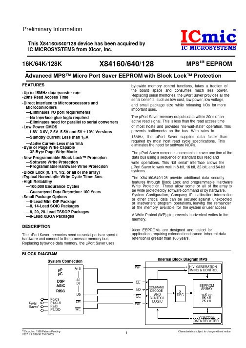
元器件交易网Preliminary InformationThis X84160/640/128 device has been acquired by IC MICROSYSTEMS from Xicor, Inc.ICmicTMIC MICROSYSTEMS16K/64K/128KX84160/640/128MPSTM EEPROMAdvanced MPS™ Micro Port Saver EEPROM with Block Lock™ ProtectionFEATURES•Up to 15MHz data transfer rate •20ns Read Access Time •Direct Interface to Microprocessors and Microcontrollers —Eliminates I/O port requirements —No interface glue logic required —Eliminates need for parallel to serial converters •Low Power CMOS —1.8V–3.6V, 2.5V–5.5V and 5V ± 10% Versions —Standby Current Less than 1µA —Active Current Less than 1mA •Byte or Page Write Capable —32-Byte Page Write Mode •New Programmable Block Lock™ Protection —Software Write Protection —Programmable Hardware Write Protection •Block Lock (0, 1/4, 1/2, or all of the array) •Typical Nonvolatile Write Cycle Time: 3ms •High Reliability —100,000 Endurance Cycles —Guaranteed Data Retention: 100 Years •Small Package Options —8-Lead Mini-DIP Package —8, 14-Lead SOIC Packages —8, 20, 28-Lead TSSOP Packages —8-Lead XBGA Packagesbytewide memory control functions, takes a fraction of the board space and consumes much less power. Replacing serial memories, the µPort Saver provides all the serial benefits, such as low cost, low power, low voltage, and small package size while releasing I/Os for more important uses. The µPort Saver memory outputs data within 20ns of an active read signal. This is less than the read access time of most hosts and provides “no-wait-state” operation. This prevents bottlenecks on the bus. With rates to 15MHz, the µPort Saver supplies data faster than required by most host read cycle specifications. This eliminates the need for software NOPs. The µPort Saver memories communicate over one line of the data bus using a sequence of standard bus read and write operations. This “bit serial” interface allows the µPort Saver to work well in 8-bit, 16 bit, 32-bit, and 64-bit systems. The X84160/640/128 provide additional data security features through Block Lock and programmable Hardware Write Protection. These allow some or all of the array to be write protected by software command or by hardware. System Configuration, Company ID, calibration information, or other critical data can be secured against unexpected or inadvertent program operations, leaving the remainder of the memory available for the system or user access A Write Protect (WP) pin prevents inadvertent writes to the memory. Xicor EEPROMs are designed and tested for applications requiring extended endurance. Inherent data retention is greater than 100 years.DESCRIPTIONThe µPort Saver memories need no serial ports or special hardware and connect to the processor memory bus. Replacing bytewide data memory, the µPort Saver usesBLOCK DIAGRAMSystem ConnectionµP µCA15 WPInternal Block Diagram MPSH.V. GENERATION TIMING & CONTROLDSP ASIC RISCPorts SavedP0/CS P1/CLK P2/DIA0 D7CE I/OCOMMAND DECODED0 OE WEOE WEAND CONTROLX DECEEPROM ARRAY 16K x 88K x 8 2K x 8LOGICP3/DOY DECODE DATA REGISTER© Xicor, Inc. 1998 Patents Pending7067 1.1 6/10/98 T10/C0/D31Characteristics subject to change without notice元器件交易网X84160/640/128PIN CONFIGURATIONS: Drawings are to the same scale, actual package sizes are shown in inches:8-LEAD PDIP 8-LEAD SOIC CE I/O WP V SS 1 2 X84160 3 X84640 4 .230 in. 8 7 6 5 V CC NC OE WE .190 in. NC VCC CE I/O 8-LEAD TSSOP 1 2 3 4 8 7 6 5 OE WE WP VSSPIN NAMES.114 in.X84160I/O CE OE WE WPData Input/Output Chip Enable Input Write Enable Input Supply Voltage Ground Output Enable Input Write Protect Input14-LEAD SOIC CE I/O NC NC NC WP V SS 1 2 3 4 5 6 7 .230 in. X84128 14 13 12 11 10 9 8 V CC NC NC NC NC OE WE .390 in.NC NC CE I/O NC NC NC WP VSS NC1 2 3 4 5 6 7 8 9 10X8464020 19 18 17 16 15 14 13 12 11NC NC VCC NC NC NC NC OE WE NC.250 in.roNC NC NC NC VCC NC NC .394 in. NC NC OE WE NC NC NC.252 in. 28-LEAD TSSOP NC NC CE CE CE I/O NC NC NC WP VSS NC NC NC 1 2 3 4 5 6 7 8 9 10 11 12 13 14 28 27 26 25 24 23 22 21 20 19 18 17 16 158-LEAD XBGA: Top View VCC 1 8 I/O .238 in. NC WE OE 2 7 CE 3 6 VSS 4 5 WPP2X84128e. 252 in..078 in.PIN DESCRIPTIONS Chip Enable (CE)ol etThe Chip Enable input must be LOW to enable all read/ write operations. When CE is HIGH, the chip is deselected, the I/O pin is in the high impedance state, and unless a nonvolatile write operation is underway, the device is in the standby power mode. Output Enable (OE) The Output Enable input must be LOW to enable the output buffer and to read data from the device on the I/O line.bsWrite Protect (WP) The Write Protect input controls the Hardware Write Protect feature. When WP is LOW and the nonvoltaile bit WPEN is “1”, nonvolatile writes of the X84160/640/128 control register is disabled, but the part otherwise functions normally. When WP is held HIGH, all functions, including nonvolatile write operate normally. WP going LOW while CS is still LOW will interrupt a write to the X84160/640/128 control register. If the internal Write cycle has already been initiated, WP going LOW will have no effect on write. The WP pin function is blocked when the WPEN bit in the control register is “0”. This allows the user to install the X84160/640/128 in a system with WP pin grounded and still be able to write to the control register. The WP pin functions will be enabled when the WPEN bit is set “1”.OWrite Enable (WE) The Write Enable input must be LOW to write either data or command sequences to the device. Data In/Data Out (I/O) Data and command sequences are serially written to or serially read from the device through the I/O pin.du cVCC VSS NC No Connect20-LEAD TSSOPPACKAGE SELECTION GUIDE841608-Lead PDIP 8-Lead SOIC 8-Lead TSSOP 8-Lead CSP/BGA 8-Lead PDIP 8-Lead SOIC 20-Lead TSSOP 8-Lead CSP/BGA 8-Lead PDIP 14-Lead SOIC 28-Lead TSSOP8464084128t.252 in.元器件交易网X84160/640/128DEVICE OPERATION The X84160/640/128 are serial EEPROMs designed to interface directly with most microprocessor buses. Standard CE, OE, and WE signals control the read and write operations, and a single l/O line is used to send and receive data and commands serially. Data Timing Data input on the l/O line is latched on the rising edge of either WE or CE, whichever occurs first. Data output on the l/O line is active whenever both OE and CE are LOW. Care should be taken to ensure that WE and OE are never both LOW while CE is LOW. Read Sequence A read sequence consists of sending a 16-bit address followed by the reading of data serially. The address is written by issuing 16 separate write cycles (WE and CE LOW, OE HIGH) to the part without a read cycle between the write cycles. The address is sent serially, most significant bit first, over the I/O line. Note that this sequence is fully static, with no special timing restrictions, and the processor is free to perform other tasks on the bus whenever the device CE pin is HIGH. Once the 16 address bits are sent, a byte of data can be read on the I/O line by issuing 8 separate read cycles (OE and CE LOW, WE HIGH). At this point, writing a ‘1’ will terminate the read sequence and enter the low power standby state, otherwise the device will await further reads in the sequential read mode. Sequential Read The byte address is automatically incremented to the next higher address after each byte of data is read. The data stored in the memory at the next address can be read sequentially by continuing to issue read cycles. When the highest address in the array is reached, the address counter rolls over to address 0000h and reading may be continued indefinitely. Reset Sequence The reset sequence resets the device and sets an internal write enable latch. A reset sequence can be sent at any time by performing a read/write “0”/read operation (see Figs. 1 and 2). This breaks the multiple read or write cycle sequences that are normally used to read from or write to the part. The reset sequence can be used at any time to interrupt or end a sequential read or page load. As soon as the write “0” cycle is complete, the part is reset (unless a nonvolatile write cycle is in progress). The second read cycle in this sequence, and any further read cycles, will read a HIGH on the l/O pin until a valid read sequence (which includes the address) is issued. The reset sequence must be issued at the beginning of both read and write sequences to be sure the device initiates these operations properly.Figure 1. Read SequenceCEObsOEWEol etI/O (IN)"0"A15 A14 A13 A12 A11 A10 A9 A8eP3A7 A6 A5 A4 A3 A2I/O (OUT) RESETWHEN ACCESSING: X84160 ARRAY: A15–A11=0 X84640 ARRAY: A15–A13=0 X84128 ARRAY: A15–A14=0LOAD ADDRESSroA1 A0du cD7 D6 D5 D4 D3 D2 D1 D0READ DATAt7008 FRM F04.1元器件交易网X84160/640/128Figure 2: Write SequenceCEOEWEI/O (IN)"0"A15 A14 A13 A12 A11 A10 A9 A8A7 A6 A5 A4 A3 A2 A1 A0du cD7 D6 D5 D4 D3 D2 D1 D0RESETWHEN ACCESSING: X84160 ARRAY: A15–A11=0 X84640 ARRAY: A15–A13=0 X84128 ARRAY: A15–A14=0LOAD ADDRESSroI/O (OUT)LOAD DATAP4ol etWrite Sequence A nonvolatile write sequence consists of sending a reset sequence, a 16-bit address, up to 32 bytes of data, and then a special “start nonvolatile write cycle” command sequence.epage, where data loading can continue. For this reason, sending more than 256 consecutive data bits will result in overwriting previous data. A nonvolatile write cycle will not start if a partial or incomplete write sequence is issued. The internal write enable latch is reset when the nonvolatile write cycle is completed and after an invalid write to prevent inadvertent writes. Note that this sequence is fully static, with no special timing restrictions. The processor is free to perform other tasks on the bus whenever the chip enable pin (CE) is HIGH. Nonvolatile Write Status The status of a nonvolatile write cycle can be determined at any time by simply reading the state of the l/O pin on the device. This pin is read when OE and CE are LOW and WE is HIGH. During a nonvolatile write cycle the l/O pin is LOW. When the nonvolatile write cycle is complete, the l/O pin goes HIGH. A reset sequence can also be issued during a nonvolatile write cycle with the same result: I/O is LOW as long as a nonvolatile write cycle is in progress, and l/O is HIGH when the nonvolatile write cycle is done.The nonvolatile write cycle is initiated by issuing a special read/write “1”/read sequence. The first read cycle ends the page load, then the write “1” followed by a read starts the nonvolatile write cycle. The device recognizes 32byte pages (e.g., beginning at addresses XXXXXX00000 for X84160). When sending data to the part, attempts to exceed the upper address of the page will result in the address counter “wrapping-around” to the first address on theObsThe reset sequence is issued first (as described in the Reset Sequence section) to set an internal write enable latch. The address is written serially by issuing 16 separate write cycles (WE and CE LOW, OE HIGH) to the part without any read cycles between the writes. The address is sent serially, most significant bit first, on the l/O pin. Up to 32 bytes of data are written by issuing a multiple of 8 write cycles. Again, no read cycles are allowed between writes.t"1" "0" START NONVOLATILE WRITE7008 FRM F05.1元器件交易网X84160/640/128CONTROL REGISTER The X84160/640/128 has one register that contains control bits for the devices. The control bits, WPEN, BP1, and BP0, are shown in Table 1. To read or change the contents of this register requires a one byte operation to address FFFFh. A read from FFFFh returns the one byte contents of the control register unused bits return 0. Continued reads return undefined data. A write to address FFFFh changes the value of the bits. Unused bits are written as “0”. Writing more than one byte to the control register is a violation and the operation will be aborted. After sending one byte to the control register, a start nonvolatile write cycle will latch in the new state. Table 1 7 WPEN 6 0 5 0 4 0 3 BP1 2 BP0 1 0 0 0 The Write Protect (WP) pin and the nonvolatile Write Protect Enable (WPEN) bit in the Status Register control the programmable hardware write protect feature. Hardware write protection is enabled when WP pin is LOW, and the WPEN bit is “1”. Hardware write protection is disabled when either the WP pin is HIGH or the WPEN bit is “0”. When the chip is hardware write protected, nonvolatile write is disabled to the Control Register, including the Block Protect bits and the WPEN bit itself, as well as the block-protected sections in the memory array. Only the sections of the memory array that are not block-protected can be written.Note: When the WP pin is tied to VSS and the WPEN bit is HIGH, the WPEN bit is write protected. It cannot be changed back to a “0”, as long as the WP pin is held LOW.WPEN 0 1 XWP X LOW HIGHProtected Blocks Protected ProtectedUnprotected Blocks Writable WritableProtectedTable 3. Block Lock ProtectionbsControl Register Bits BP1 0 0 1 1 BP0 0 1 0 1ol etWritableeWPEN: Write Protect Enable Bit The Write-Protect-Enable (WPEN) bit is an enable bit for the WP pin. Table 2Status Register WritableBP1, BP0: Block Protect Bits The Block Protect (BP0 and BP1) bits are nonvolatile and allow the user to select one of four levels of protection. The X84160/640/128 is divided into four segments. One, two, or all four of the segments may be protected. That is, the user may read the segments but will be unable to alter (write) data within the selected segments. The partitioning is controlled as illustrated in table 3 below.Protected WritableX84160 None 0600h–07FFh 0400h–07FFh 0000–07FFhPX84640 None5Array Address Protected X84128 None 3000h–3FFFh 2000h–3FFFh 0000h–3FFFh upper 1/4 upper 1/2 Full Array (Not including the control register.) Array1800h–1FFFh 1000h–1FFFh 0000–1FFFhOrodu ct元器件交易网X84160/640/128Low Power Operation The device enters an idle state, which draws minimal current when: —an illegal sequence is entered. The following are the more common illegal sequences: • Read/Write/Write—any time • Read/Write ‘1’—When writing the address or writing data. • Write ‘1’—when reading data • Read/Read/Write ‘1’—after data is written to device, but before entering the NV write sequence. —the device powers-up; —a nonvolatile write operation completes. While a sequential read is in progress, the device remains in an active state. This state draws more current than the idle state, but not as much as during a read itself. To go back to the lowest power condition, an invalid condition is created by writing a ‘1’ after the last bit of a read operation. Write Protection The following circuitry has been included to prevent inadvertent nonvolatile writes: —The internal Write Enable latch is reset upon power-up. —A reset sequence must be issued to set the internal write enable latch before starting a write sequence. —A special “start nonvolatile write” command sequence is required to start a nonvolatile write cycle.—The internal Write Enable latch is reset and remains reset as long as the WP pin is LOW, which blocks all nonvolatile write cycles. —The internal Write Enable latch resets on an invalid write operation. SYMBOL TABLEroWAVEFORM 6PeObsol etdu cINPUTS Must be steady May change from LOW to HIGH May change from HIGH to LOW Don’t Care: Changes Allowed N/A Will be steadyOUTPUTSWill change from LOW to HIGH Will change from HIGH to LOW Changing: State Not Known Center Line is High Impedancet—The internal Write Enable latch is reset automatically at the end of a nonvolatile write cycle.元器件交易网X84160/640/128ABSOLUTE MAXIMUM RATINGS* Temperature under Bias ...................... –65°C to +135°C Storage Temperature ........................... –65°C to +150°C Terminal Voltage with Respect to VSS .......................................–1V to +7V DC Output Current................................................... 5mA Lead Temperature (Soldering, 10 seconds)..........300°C RECOMMENDED OPERATING CONDITIONS Temperature Commercial Industrial Min. 0°C –40°C Max. +70°C +85°C +125°C *COMMENT Stresses above those listed under “Absolute Maximum Ratings” may cause permanent damage to the device. This is a stress rating only and the functional operation of the device at these or any other conditions above those indicated in the operational sections of this specification is not implied. Exposure to absolute maximum rating conditions for extended periods may affect device reliability. Supply Voltage X84160/640/128X84160/640/128 – 2.5 X84160/640/128 – 1.8D.C. OPERATING CHARACTERISTICS (VCC = 5V ±10%) (Over the recommended operating conditions, unless otherwise specified.) Symbol ICC1 Parameter VCC Supply Current (Read) Min.PMax. 12 1 10 10 VCC x 0.3 VCC + 0.5 0.47LimitsroUnits mA Test Conditions OE = VIL, WE = VIH, I/O = Open, CE clocking = VCC x 0.1/VCC x 0.9 @ 10 MHzICC During Nonvolatile Write Cycle All Inputs at CMOS Levels CE = VCC, Other Inputs = VCC or VSS VIN = VSS to VCC VOUT = VSS to VCC mA µA µA µA V V V V IOL = 2.1mA IOH = –1mAMilitary† –55°C Notes: † Contact factory for Military availabilityISB1 ILI ILO VlL (1) VIH(1)VCC Standby CurrentInput Leakage CurrentOutput Leakage Current Input LOW VoltageInput HIGH VoltagebsVOLOutput LOW Voltage Output HIGH Voltage VCC – 0.8VOHNotes: (1) VIL Min. and VIH Max. are for reference only and are not tested.Ool etICC2VCC Supply Current (Write)e–0.5VCC x 0.7du ctLimits 4.5V to 5.5V 2.5V to 5.5V 1.8V to 3.6V元器件交易网X84160/640/128D.C. OPERATING CHARACTERISTICS (VCC = 2.5V to 5.5V) (Over the recommended operating conditions, unless otherwise specified.) Symbol Parameter Limits Min. Max. 300 Units Test Conditions OE = VIL, WE = VIH, I/O = Open, CE clocking = VCC x 0.1/VCC x 0.9 @ VCC = 2.5, 5 MHz ICC During Nonvolatile Write Cycle All Inputs at CMOS Levels CE = VCC, Other Inputs = VCC or VSS VIN = VSS to VCC VOUT = VSS to VCCICC1VCC Supply Current (Read)µAICC2 ISB1 ILI ILO VlL(1) VIH(1) VOL VOHVCC Supply Current (Write) VCC Standby Current Input Leakage Current Output Leakage Current Input LOW Voltage Input HIGH Voltage Output LOW Voltage Output HIGH Voltage VCC – 0.4 –0.5 VCC x 0.72 1 10 10 VCC x 0.3mA µA µA µA VVCC + 0.5 0.4PMax. 200 1 1 10 10 VCC x 0.3 VCC + 0.5 0.48ol etSymbolParametereD.C. OPERATING CHARACTERISTICS (VCC = 1.8V to 3.6V) (Over the recommended operating conditions, unless otherwise specified.) Limits Min. Units Test Conditions OE = VIL, WE = VIH, I/O = Open, CE clocking = VCC x 0.1/VCC x 0.9 @ VCC = 1.8V, 4 MHz ICC During Nonvolatile Write Cycle All Inputs at CMOS Levels CE = VCC, Other Inputs = VCC or VSS VIN = VSS to VCC VOUT = VSS to VCCICC1VCC Supply Current (Read)ICC2 ISB1 ILI ILOVCC Supply Current (Write) VCC Standby CurrentbsInput Leakage Current Output Leakage Current Input LOW Voltage Input HIGH Voltage Output LOW Voltage Output HIGH Voltage VCC – 0.2 –0.5 VCC x 0.7VlL(1)OVIH(1) VOL VOHNotes: (1) VIL Min. and VIH Max. are for reference only and are not tested.roV V V µA mA µA µA µA V V V Vdu cIOL = 1mA, VCC = 3V IOH = –400µA, VCC = 3V IOL = 0.5mA, VCC = 2V IOH = –250µA, VCC = 2Vt元器件交易网X84160/640/128CAPACITANCE Symbol CI/O(2) CIN(2) TA = +25°C, f = 1MHz, VCC = 5V Parameter Input/Output Capacitance Input Capacitance Max. 8 6 Units pF pF Test Conditions VI/O = 0V VIN = 0VPOWER-UP TIMING Symbol tPUR(3) tPUW(3) Parameter Power-up to Read Operation Power-up to Write OperationA.C. CONDITIONS OF TEST Input Pulse Levels Input Rise and Fall Times Input and Output Timing Levels5nsVCC x 0.5EQUIVALENT A.C. LOAD CIRCUITS5V 2.06KΩ OUTPUT 3.03KΩol eteP3V 2.8K Ω OUTPUT 30pF 5.6K Ω 30pF 2V9VCC x 0.1 to VCC x 0.92.39KΩOUTPUT30pF4.58KΩObsroNotes: (3) Time delays required from the time the VCC is stable until the specific operation can be initiated. Periodically sampled, but not 100% tested.du cMax. 2 5Notes: (2) Periodically sampled, but not 100% tested.tUnits ms ms元器件交易网X84160/640/128A.C. CHARACTERISTICS (Over the recommended operating conditions, unless otherwise specified.) Read Cycle Limits – X84160/640/128 VCC = 4.5V – 5.5V VCC = 2.5V – 5.5V VCC = 1.8V – 3.6V SymboltRC tCE tOE tOEL tOEH tLOW tHIGH tLZ(4)ParameterRead Cycle Time CE Access Time OE Access Time OE Pulse Width OE High Recovery Time CE LOW Time CE HIGH Time CE LOW to Output In Low Z CE HIGH to Output In High Z OE LOW to Output In Low Z OE HIGH to Output In High Z Output Hold from CE or OE HIGH WE HIGH Setup Time WE HIGH Hold TimeMin.70MaxMin.125Max.Min.25020 20 20 50 20 50 0 0 0 0 0 25 15 35 90 35 90 0du c25 70 25 70 70 180 70 180 0 0 0 25 0 0 25 25 30 30 25t OEH t OHZ HIGH Z t HZro0 0 0 0 25 25tHIGH tWEH tOHtHZ(4) tOLZ(4) tOHZ tOH tWES tWEH(4)P15e25Notes: (4) Periodically sampled, but not 100% tested. tHZ and tOHZ are measured from the point where CE or OE goes HIGH (whichever occurs first) to the time when I/O is no longer being driven into a 5pF load.ol ettRC tLOWtCECEbsWEtWES tOEt OELOEOI/Ot OLZ t LZDATA10tMax.Unitsns ns ns ns ns ns ns ns ns ns ns ns ns nsOb so l et ePr od u ctX84160/640/128Write Cycle Limits – X84160/640/128Notes:(5)t NVWC sequence until the self-timed, internal nonvolatile write cycle is completed.(6)Data is latched into the X84160/640/128 on the rising edge of CE or WE, whichever occurs first.(7)Periodically sampled, but not 100% tested.Symbol ParameterV CC = 4.5V – 5.5V V CC = 2.5V – 5.5V V CC = 1.8V – 3.6VUnits Min.Max.Min.Max.Min.Max.t NVWC (5)Nonvolatile Write Cycle Time 555ms t WCWrite Cycle Time70125250nst WP WE Pulse Width203550ns t WPH WE HIGH Recovery Time 5090180ns t CS Write Setup Time 000ns t CH Write Hold Time 000ns t CP CE Pulse Width203570ns t CPH CE HIGH Recovery Time 5090180ns t OES OE HIGH Setup Time 252550ns t OEH OE HIGH Hold Time 252550ns t DS (6)Data Setup Time 122030ns t DH (6)Data Hold Time 555ns t WPSU (7)WP HIGH Setup 100100150ns t WPHD (7)WP HIGH Hold100100150nsX84160/640/128CE Controlled Write CycleWE Controlled Write CycleOb soctX84160/640/1288-LEAD XBGA TYPE430±20X84640Z: Bottom ViewNOTE: ALL DIMENSIONS IN µMALL DIMENSIONS ARE TYPICAL VALUES20Ob soctX84160/640/1288-LEAD XBGA TYPEX84128: Bottom ViewNOTE: ALL DIMENSIONS IN µMALL DIMENSIONS ARE TYPICAL VALUES20Ob s octX84160/640/128NO TE:1.ALL DIMENSIONS IN INCHES (IN PARENTHESES IN MILLIMETERS)2.PACKAGE DIMENSIONS EXCLUDE MOLDING FLASHTYP .8-LEAD PLASTIC DUAL IN-LINE P ACKAGE TYPE PHALF SHOULDER ALL MAX.X84160/640/1288-LEAD PLASTIC SMALL OUTLINE GULL WING P ACKAGE TYPE SNOTE: ALL DIMENSIONS IN INCHES (IN PARENTHESES IN MILLIMETERS)X84160/640/128PACKAGING INFORMATION14-LEAD PLASTIC SMALL OUTLINE GULL WING P ACKAGE TYPE SNOTE: ALL DIMENSIONS IN INCHES (IN PARENTHESES IN MILLIMETERS)Ob sou ctX84160/640/128PACKAGING INFORMATIONNOTE:ALL DIMENSIONS IN INCHES (IN P ARENTHESES IN MILLIMETERS)8-LEAD PLASTIC, TSSOP , PACKAGE TYPE V0° – 8°Ob so lt u ctX84160/640/128PACKAGING INFORMATIONNOTE:ALL DIMENSIONS IN INCHES (IN P ARENTHESES IN MILLIMETERS)20-LEAD PLASTIC, TSSOP PACKAGE TYPE V0° – 8Gage Plane Seating PlaneOb so lu ctX84160/640/128PACKAGING INFORMATIONNOTE:ALL DIMENSIONS IN INCHES (IN P ARENTHESES IN MILLIMETERS)28-LEAD PLASTIC, TSSOP PACKAGE TYPE V0° – 8Gage Plane Seating PlaneX84160/640/128LIMITED WARRANTYDevices sold by Xicor, Inc. are covered by the warranty and patent indemnification provisions appearing in its Terms of Sale only. Xicor, Inc. makes no warranty, express, statutory, implied, or by description regarding the information set forth herein or regarding the freedom of the described devices from patent infringement. Xicor, Inc. makes no warranty of merchantability or fitness for any purpose. Xicor, Inc. reserves the right to discontinue production and change specifications and prices at any time and without notice.Xicor, Inc. assumes no responsibility for the use of any circuitry other than circuitry embodied in a Xicor, Inc. product. No other circuits, patents, licenses are implied.U.S. PATENTSXicor products are covered by one or more of the following U.S. Patents: 4,263,664; 4,274,012; 4,300,212; 4,314,265; 4,326,134; 4,393,481; 4,404,475;4,450,402; 4,486,769; 4,488,060; 4,520,461; 4,533,846; 4,599,706; 4,617,652; 4,668,932; 4,752,912; 4,829, 482; 4,874, 967; 4,883, 976. Foreignpatents and additional patents pending.LIFE RELATED POLICYIn situations where semiconductor component failure may endanger life, system designers using this product should design the system with appropriate error detection and correction, redundancy and back-up features to prevent such an occurence.Xicor's products are not authorized for use in critical components in life support devices or systems.1. Life support devices or systems are devices or systems which, (a) are intended for surgical implant into the body, or (b) support or sustainlife, and whose failure to perform, when properly used in accordance with instructions for use provided in the labeling, can be reasonably expected to result in a significant injury to the user.2. A critical component is any component of a life support device or system whose failure to perform can be reasonably expected to cause the failureof the life support device or system, or to affect its safety or effectiveness.22。
袋式除尘器型号之欧阳道创编

14
YLC 84-2×8
196800~207360
3280
16
YLC 84-2×9
221400~265680
3690
18
YLC 84-2×10
246000~295200
4100
20
YLC 160-2*4
288000~345600
3856
10
160*6000
YLC 160-2*5
288000~600
26.4
128-10
112100
1558
1280
6.0
2053
28.9
128-2×6
34600
1869
1536
7.0
323
36.6
128-2×7
157000
2181
1792
8.3
247
43.9
128-2×8
179400
2492
2048
9.5
262
50.0
128-2×9
201900
2804
2304
10.7
2150
2540
2880
气箱脉冲袋式除尘器技术参数:
型号
处理风量
(m3/h)
滤袋风速
(m/min)
过滤面积
(m2)
滤袋数
(个)
耗气量
(m3/min)
阻力
(Pa)
含尘浓度
(g/m3)
保温层面
积(m2)
重量
(t)
32-3
6900
1.2-2.0
93
96
0.27
1470-
1770
萨姆巴全功能PLC系列产品说明书

Samba™ models - Onboard I/Os
Article
summary
Digital2
HSC/Shaftencoder 2
Inputs 1 Analog
Temperature Measurement
Transistor 3
SM35-J-R20 SM43-J-R20 SM70-J-R20
2 PT100/TC
None
None
8
0-10V, 4-20mA, 12-bit
24VDC
SM35-J-TA22 12 Digital, 1 HSC/Shaft-
SM43-J-TA22* encoder, 2 AI, 2 PT100/TC,
SM70-J-TA22*
8 Transistor, 2 AO
Keys
Displays virtual keyboard when the application requires data entry
General
Power Supply
24VDC
Battery
7 years typical at 77°F, battery back-up for RTC and system data, including variable data
No PC needed
PLC
• I/O options: Digital, Analog, including High-speed • Auto-tune PID, 2 independent loops • Recipe programs and data logging via Data Tables • Date & Time-based control
MB85RC64中文

铁电存储器MB85RC64(8K×8)1.概述MB85RC64了FRAM(铁电随机存取记忆体)独立芯片配置了8192×8位,形成铁电工艺和硅栅CMOS工艺技术非易失性内存中的细胞。
MB85RC64采用两线串行接口(与世界标准的I2C总线兼容)。
与SRAM不同的MB85RC64是无需使用数据备份电池,能够保留数据。
MB85RC64的读写次数10亿次,与EPROM和FLASH相比,有显著的改善。
而且不在向写完存储器后,不需要查询序列。
2.特性●位操作:8192×8位●工作电压:2.7V—3.3V●工作频率:400KHz●两串行总线:I2C总线2.1标准版,支持标准模式和快速模式,由SCL和SDA控制。
●工作温度范围:-40℃—85℃●数据保持:10年(55℃)●读写寿命:至少每位10亿次●封装:Plastic / SOP, 8-pin (FPT-8P-M02)●低电压消耗:工作电流0.15mA,待机电流5uA3.管脚分配3.管脚功能描述4.模块框图5.I2C 电路MB85RC64有两线串行接口,支持I2C 总线,并作为从器件工作。
I2C 总线定义的“主机”和“从机”设备的沟通角色,主机启动总线控制权。
此外,通过I2C 总线,在一个主机可以连接多个从器件。
在这种情况下,必须给从器件分配一个唯一的设备地址。
6.I2C通信协议I2C总线是双线串行接口,采用了双向数据总线(SDA)和串行时钟(SCL)。
数据传输只能由总线主机,这也将提供串行时钟的同步启动。
SCL为低电平时,SDA信号应该改变。
然而,作为一种例外,启动和停止时的通信序列,SDA被允许改变当SCL为高电平。
●启动条件:开始时,SCL为稳定高电平,SDA产生下降沿。
●停止条件:停止时,SCL为稳定低电平,SDA产生上升沿。
停止条件是终止从设备和主机通信。
MB85RC64不需要像内部写存储器像E2PROM花时间去查询序列,因此当写停止命令结束,设备进入待机模式。
- 1、下载文档前请自行甄别文档内容的完整性,平台不提供额外的编辑、内容补充、找答案等附加服务。
- 2、"仅部分预览"的文档,不可在线预览部分如存在完整性等问题,可反馈申请退款(可完整预览的文档不适用该条件!)。
- 3、如文档侵犯您的权益,请联系客服反馈,我们会尽快为您处理(人工客服工作时间:9:00-18:30)。
DESCRIPTIONThe MH8S64AQFC is 8388608 - word by 64-bit Synchronous DRAM module. This consists of four industry standard 8Mx16 Synchronous DRAMs in TSOP and one industory standard EEPROM in TSSOP.The mounting of TSOP on a card edge Dual Inline package provides any application where high densities and large quantities of memory are required.This is a socket type - memory modules, suitablefor easy interchange or addition of modules.FEATURESMax. Clock frequency -6:133MHz,-7,8:100MHzsingle 3.3V±0.3V power supplyBurst length- 1/2/4/8/Full Page(programmable)(Front)(Back)12143144PCB OutlineFrequencyCLK Access Time-8,-8L100MHz 6.0ns(CL=2)(Component SDRAM)6.0ns(CL=3)100MHz-7,-7L 5.4ns(CL=3)-6,-6L 133MHzNC = No ConnectionPIN CONFIGURATIONPINNumberFront side Pin NameBack side Pin NamePINNumber1357911131517192468101214161820PINNumberFront side Pin NameBack side Pin NamePINNumber73747576777879808182838485868788899091922122939423249596252697982728991002930101102313210310433341051063536107108373810911039401111124142113114434411511645461171184748119120495012112251521231245354125126555612712857581291305960131132616213313463641351366566137138676813914069701411427172143144Vss DQ0DQ1DQ2DQ3Vcc DQ4DQ5DQ6DQ7Vss DQ32DQ33DQ34DQ35Vcc DQ36DQ37DQ38DQ39NC CLK1Vss Vss NC NC NC NC Vcc Vcc DQ16DQ48DQ17DQ49DQ18DQ50DQ19DQ51Vss Vss Vss Vss DQ20DQ52DQMB0DQMB4DQ21DQ53DQMB1DQMB5DQ22DQ54Vcc Vcc DQ23DQ55A 0A 3Vcc Vcc A 1A 4A 6A 7A 2A 5A 8BA 0Vss Vss Vss Vss DQ8DQ40A 9BA 1DQ9DQ41A 10A 11DQ10DQ42Vcc Vcc DQ11DQ43DQMB2DQMB6Vcc Vcc DQMB3DQMB7DQ12DQ44Vss Vss DQ13DQ45DQ24DQ56DQ14DQ46DQ25DQ57DQ15DQ47DQ26DQ58Vss Vss DQ27DQ59NC NC Vcc Vcc NC NC DQ28DQ60CLK0CKE0DQ29DQ61Vcc Vcc DQ30DQ62/RA S /CA S DQ31DQ63/WE CKE1Vss Vss /S0NC SDA SCL /S1NCVccVccCLK0SCL VccVssD0 - D3D0 - D3DQMB1CKE0D0 - D3/RASD0 - D3/CASD0 - D3/WED0 - D3BA0,BA1,A<11:0>D0 - D3CLK1Serial Presence Detect Table IByte Function describedSPD enrty dataSPD DATA(hex )0Defines # bytes written into serial memory at module mfgr128801Total # bytes of SPD memory device256 Bytes 082Fundamental memory type SDRAM 043# Row Addresses on this assembly A0-A110C 4# Column Addresses on this assembly A0-A8095# Module Banks on this assembly 1BANK 016Data Width of this assembly...x64407... Data Width continuation0008Voltage interface standard of this assemblyLVTTL 019SDRAM Cycletime at Max.Supported CAS Latency (CL).A0Cy cle time for CL=310SDRAM Access from Clock6ns60tAC for CL=311DIMM Configuration type (Non-parity,Parity,ECC)Non-PARITY0012Refresh Rate/Type self refresh(15.625uS)8013SDRAM width,Primary DRAM x161014Error Checking SDRAM data widthN/A 0015Minimum Clock Delay,Back to Back Random Column Addresses10116Burst Lengths Supported 1/2/4/8/Full page8F 17# Banks on Each SDRAM device4bank 0418CAS# Latency 2/30619CS# Latency 00120Write Latency 00121SDRAM Module Attributes non-buffered,non-registered 0022SDRAM Dev ice Attributes:GeneralPrecharge All,Auto precharge0E 23SDRAM Cycle time(2nd highest CAS latency)13ns D0Cy cle time for CL=224SDRAM Access form Clock(2nd highest CAS latency)7ns 70tAC for CL=225SDRAM Cycle time(3rd highest CAS latency)N/A 00N/A 0026SDRAM Access form Clock(3rd highest CAS latency)10ns -8,-8L -8,-8L10ns A06ns 607.5ns 5.4ns -6,-6L -7,-7L,-8,-8L -6,-6L -7,-7L,-8,-8L7554-6,-6L,-7,-7L -6,-6L,-7,-7L 27Precharge to Active Minimum 20ns 1428Row Active to Row Active Min.15ns 0F 29RAS to CAS Delay Min 22.5ns 1730Active to Precharge Min50ns3222.5ns 1720ns 1420ns 1445ns 2D -6,-6L-7,-7L,-8,-8L -6,-6L -7,-7L,-8,-8L -6,-6L -7,-7L,-8,-8L -6,-6L -7,-7L,-8,-8LSerial Presence Detect Table II31Density of each bank on module64MByte 1036-61Superset Information (may be used in future)option 0062SPD Revision 63Checksum for bytes 0-62Check sum for -8,-8L4D64-71Manufactures Jedec ID code per JEP-108EMITSUBISHI 1CFFFFFFFFFFFFFF72Manufacturing locationMiyoshi,Japan 01Tajima,Japan 02NC,USA 03Germany 0473-90Manufactures Part NumberMH8S64AQFC-8MH8S64AQFC-8L91-92Rev ision Code PCB rev ision rrrr 93-94Manufacturing date year/week code yyww 95-98Assembly Serial Number serial numberssssssss99-125Manufacture Specific Data option 00126Intetl specification frequency 100MHz64127Intel specification CAS# Latency support128+Unused storage locationsopen0032Command and Address signal input setup time33Command and Address signal input hold time34Data signal input setup time35Data signal input hold timerev 1.2B 12Check sum for -7,-7L 0D MH8S64AQFC-74D4838533634415146432D37202020202020-6,-6L,-7,7L 8F -8,8L8D MH8S64AQFC-7L 4D4838533634415146432D374C20202020204D4838533634415146432D382020202020204D4838533634415146432D384C202020202020201010150815082ns 1ns 2ns 1ns 1.5ns 0.8ns 1.5ns 0.8ns Check sum for -6,-6L AC MH8S64AQFC-6MH8S64AQFC-6L-6,-6L -7,-7L,-8,-8L-6,-6L -7,-7L,-8,-8L-6,-6L -7,-7L,-8,-8L -6,-6L-7,-7L,-8,-8LCL=2/3,AP,CK0,1CL=3,AP,CK0,14D4838533634415146432D364C20202020204D4838533634415146432D36202020202020PIN FUNCTIONBASIC FUNCTIONS/S Chip Select : L=select, H=deselect /RAS Command /CAS Command /WE CommandCKE Ref resh Option @ref resh commandA10Precharge Option @precharge or read/write commandCK def ine basic commandsThe MH8S64AQFC provides basic functions,bank(row)activate,burst read / write, bank(row)precharge,and auto / self refresh.Each command is defined by control signals of /RAS,/CAS and /WE at CK rising edge. In addition to 3 signals,/S,CKE and A10 are used as chip select,refresh option,and precharge option,respectively.To know the detailed definition of commands please see the command truth table.Activate(ACT) [/RAS =L, /CAS = /WE =H]Read(READ) [/RAS =H,/CAS =L, /WE =H]Write(WRITE) [/RAS =H, /CAS = /WE =L]Precharge(PRE) [/RAS =L, /CAS =H,/WE =L]Auto-Refresh(REFA) [/RAS =/CAS =L, /WE =CKE =H]ACT command activates a row in an idle bank indicated by BA. READ command starts burst read from the active bank indicated by BA.First output data appears after /CAS latency. When A10 =H at this command,the bank is deactivated after the burst read(auto-precharge,READA ). WRITE command starts burst write to the active bank indicated by BA. Total datalength to be written is set by burst length. When A10 =H at this command, the bank is deactivated after the burst write(auto-precharge,WRITEA ). PRE command deactivates the active bank indicated by BA. This command also terminates burst read / write operation. When A10 =H at this command, both banks are deactivated(precharge all, PREA ).PEFA command starts auto-refresh cycle. Refresh address including bank address are generated internally. After this command, the banks are precharged automatically.H =High Level, L = Low Level, V = Valid, X = Don't Care, n = CK cycle number NOTE:1.A7-9 = 0, A0-6 = Mode AddressCOMMAND TRUTH TABLECOMMAND MNEMONIC CKE n-1CKE n /S /RAS /CAS /WE BA0,1A10A0-9Deselect DESEL H X H X X X X X X No Operation NOP H X L H H H X X X Row Adress Entry &Bank Activate ACT H X L L H H V V V Single Bank Precharge PRE H X L L H L V L X Precharge All Bank PREA H X L L H L X H X Column Address Entry& Write WRITEHXLHLLVLVColumn Address Entry & Write with Auto-Precharge WRITEA H X L H L L V H VColumn Address Entry& Read READ H X L H L H V L VColumn Address Entry & Read with AutoPrecharge READA H X L H L H V H V Auto-Refres h REFA H H L L L H X X X Self-Refresh Entry REFS H L L L L H X X X Self-Refresh Exit REFSX L H H X X X X X X L H L H H H X X X Burst Terminate TERM H X L H H L X X X Mode Register SetMRSHXLLLLLLV*1A11X X V X X VV V V X X X X X LCurrent State/S/RAS/CAS/WE Address Command Action IDLE H X X X X DESEL NOPL H H H X NOP NOPL H H L BA TBST ILLEGAL*2L H L X BA,CA,A10READ/WRITE ILLEGAL*2L L H H BA,RA ACT Bank Active,Latch RAL L H L BA,A10PRE/PREA NOP*4L L L H X REFA Auto-Refresh*5L L L L Op-Code,Mode-AddMRS Mode Register Set*5ROW ACTIVE H X X X X DESEL NOP L H H H X NOP NOPL H H L BA TBST NOPL H L H BA,CA,A10READ/READA Begin Read,Latch CA, Determine Auto-PrechargeL H L L BA,CA,A10WRITE/WRITEABegin Write,Latch CA,Determine Auto-PrechargeL L H H BA,RA ACT Bank Active/ILLEGAL*2 L L H L BA,A10PRE/PREA Precharge/Precharge All L L L H X REFA ILLEGALL L L L Op-Code,Mode-AddMRS ILLEGALREAD H X X X X DESEL NOP(Continue Burst to END) L H H H X NOP NOP(Continue Burst to END)L H H L BA TBST Terminate BurstL H L H BA,CA,A10READ/READA Terminate Burst,Latch CA, Begin New Read,Determine Auto-Precharge*3L H L L BA,CA,A10WRITE/WRITEA Terminate Burst,Latch CA, Begin Write,Determine Auto-Precharge*3L L H H BA,RA ACT Bank Active/ILLEGAL*2L L H L BA,A10PRE/PREA Terminate Burst,Precharge L L L H X REFA ILLEGALL L L L Op-Code,Mode-AddMRS ILLEGALFUNCTION TRUTH TABLEFUNCTION TRUTH TABLE(continued)Current State/S/RAS/CAS/WE Address Command Action WRITE H X X X X DESEL NOP(Continue Burst to END) L H H H X NOP NOP(Continue Burst to END)L H H L BA TBST Terminate BurstL H L H BA,CA,A10READ/READA Terminate Burst,Latch CA, Begin Read,Determine Auto-Precharge*3L H L L BA,CA,A10WRITE/WRITEATerminate Burst,Latch CA,Begin Write,Determine Auto-Precharge*3L L H H BA,RA ACT Bank Active/ILLEGAL*2L L H L BA,A10PRE/PREA Terminate Burst,PrechargeL L L H X REFA ILLEGALL L L L Op-Code,Mode-AddMRS ILLEGALREAD with H X X X X DESEL NOP(Continue Burst to END) AUTO L H H H X NOP NOP(Continue Burst to END) PRECHARGE L H H L BA TBST ILLEGALL H L H BA,CA,A10READ/READA ILLEGALL H L L BA,CA,A10WRITE/WRITEAILLEGALL L H H BA,RA ACT Bank Active/ILLEGAL*2 L L H L BA,A10PRE/PREA ILLEGAL*2L L L H X REFA ILLEGALL L L L Op-Code,Mode-AddMRS ILLEGALWRITE with H X X X X DESEL NOP(Continue Burst to END) AUTO L H H H X NOP NOP(Continue Burst to END) PRECHARGE L H H L BA TBST ILLEGALL H L H BA,CA,A10READ/READA ILLEGALL H L L BA,CA,A10WRITE/WRITEAILLEGALL L H H BA,RA ACT Bank Active/ILLEGAL*2 L L H L BA,A10PRE/PREA ILLEGAL*2L L L H X REFA ILLEGALL L L L Op-Code,Mode-AddMRS ILLEGALFUNCTION TRUTH TABLE(continued)Current State/S/RAS/CAS/WE Address Command Action PRE -H X X X X DESEL NOP(Idle after tRP) CHARGING L H H H X NOP NOP(Idle after tRP) L H H L BA TBST ILLEGAL*2L H L X BA,CA,A10READ/WRITE ILLEGAL*2L L H H BA,RA ACT ILLEGAL*2L L H L BA,A10PRE/PREA NOP*4(Idle after tRP)L L L H X REFA ILLEGALL L L L Op-Code,Mode-AddMRS ILLEGALROW H X X X X DESEL NOP(Row Active after tRCD ACTIVATING L H H H X NOP NOP(Row Active after tRCD L H H L BA TBST ILLEGAL*2L H L X BA,CA,A10READ/WRITE ILLEGAL*2L L H H BA,RA ACT ILLEGAL*2L L H L BA,A10PRE/PREA ILLEGAL*2L L L H X REFA ILLEGALL L L L Op-Code,Mode-AddMRS ILLEGALWRITE RE-H X X X X DESEL NOP COVERING L H H H X NOP NOPL H H L BA TBST ILLEGAL*2L H L X BA,CA,A10READ/WRITE ILLEGAL*2L L H H BA,RA ACT ILLEGAL*2L L H L BA,A10PRE/PREA ILLEGAL*2L L L H X REFA ILLEGALL L L L Op-Code,Mode-AddMRS ILLEGALFUNCTION TRUTH TABLE(continued)Current State/S/RAS/CAS/WE Address Command Action RE-H X X X X DESEL NOP(Idle after tRC) FRESHING L H H H X NOP NOP(Idle after tRC) L H H L BA TBST ILLEGALL H L X BA,CA,A10READ/WRITE ILLEGALL L H H BA,RA ACT ILLEGALL L H L BA,A10PRE/PREA ILLEGALL L L H X REFA ILLEGALL L L L Op-Code,Mode-AddMRS ILLEGALMODE H X X X X DESEL NOP(Idle after tRSC) REGISTER L H H H X NOP NOP(Idle after tRSC) SETTING L H H L BA TBST ILLEGALL H L X BA,CA,A10READ/WRITE ILLEGALL L H H BA,RA ACT ILLEGALL L H L BA,A10PRE/PREA ILLEGALL L L H X REFA ILLEGALL L L L Op-Code,Mode-AddMRS ILLEGALABBREVIATIONS:H = Hige Level, L = Low Level, X = Don't CareBA = Bank Address, RA = Row Address, CA = Column Address, NOP = No Operation NOTES:1. All entries assume that CKE was High during the preceding clock cycle and the current clock cycle.2. ILLEGAL to bank in specified state; function may be legal in the bank indicated by BA,depending on the state of that bank.3. Must satisfy bus contention, bus turn around, write recovery requirements.4. NOP to bank precharging or in idle state.May precharge bank indicated by BA.5. ILLEGAL if any bank is not idle.ILLEGAL = Device operation and / or date-integrity are not guaranteed.FUNCTION TRUTH TABLE FOR CKECurrent State CKn-1CKn/S/RAS/CAS/WE Add ActionSELF - H X X X X X X INVALIDREFRESH*1L H H X X X X Exit Self-Refresh(Idle after tRC) L H L H H H X Exit Self-Refresh(Idle after tRC)L H L H H L X ILLEGALL H L H L X X ILLEGALL H L L X X X ILLEGALL L X X X X X NOP(Maintain Self-Refresh) POWER H X X X X X X INVALIDDOWN L H X X X X X Exit Power Down to IdleL L X X X X X NOP(Maintain Self-Refresh) ALL BANKS H H X X X X X Refer to Function Truth Table IDLE*2H L L L L H X Enter Self-Refres hH L H X X X X Enter Power DownH L L H H H X Enter Power DownH L L H H L X ILLEGALH L L H L X X ILLEGALH L L L X X X ILLEGALL X X X X X X Refer to Current State = Power Down ANY STATE H H X X X X X Refer to Function Truth Tableother than H L X X X X X Begin CK0 Suspend at Next Cycle*3 listed above L H X X X X X Exit CK0 Suspend at Next Cycle*3 L L X X X X X Maintain CK0 SuspendABBREVIATIONS:H = High Level, L = Low Level, X = Don't CareNOTES:1. CKE Low to High transition will re-enable CK and other inputs asynchronously.A minimum setup time must be satisfied before any command other than EXIT.2. Power-Down and Self-Refresh can be entered only form the All banks idle State.3. Must be legal command.SIMPLIFIED STATE DIAGRAMIDLEPRE CHARGEAUTO REFRESHSELF MODE REGISTERSETPOWER DOWNREADREADAWRITEWRITEAREAD SUSPENDREADA SUSPENDWRITE SUSPENDWRITEA SUSPENDPOWER ONCLK SUSPENDCKELCKEHCKEHCKEHACTCKEHCKELCKEHWRITEWRITEAREADAPREPOWER APPLIEDAutomatic SequencePOWER ON SEQUENCEBefore starting normal operation, the following power on sequence is necessary to prevent a SDRAM from damaged or malfunctioning.1. Apply power and start clock.Attempt to maintain CKE high,DQM0-7 high and NOP condition at the inputs.2. Maintain stable power, stable cock, and NOP input conditions for a minimum of 200us.3. Issue precharge commands for all banks. (PRE or PREA)4. After all banks become idle state (after tRP), issue 8 or more auto-refresh commands.5. Issue a mode register set command to initialize the mode register.After these sequence, the SDRAM is idle state and ready for normal operation.MODE REGISTERBurst Length, Burst Type and /CAS Latency can be programmed by setting the mode register(MRS). The mode register stores these date until the next MRS command, whichmay be issued when both banks are in idle state. After tRSC from a MRS command, the SDRAM is ready for new command.CKCommand AddressCKDQBurst TypeA2A1A0Initial AddressBLSequentialInterleavedColumn Addressing000001010011100101110111-00-01-10-11--001234567012345671234567010325476234567012301674534567012321076544567012345670123567012345476103267012345674523017012012312302301300176540123103223013201--1121345632111842CK A0-9,11A10DQOPERATION DESCRIPTIONBANK ACTIVATEOne of four banks is activated by an ACT command.An bank is selected by BA0-1. A row is selected by A0-11.Multiple banks can be active state concurrently by issuing multiple ACT commands.Minimum activation interval between one bank and another bank is tRRD.PRECHARGEAn open bank is deactivated by a PRE command.A bank to be deactivated is designated by BA0-1.When multiple banks are active, a precharge all command (PREA, PRE + A10=H) deactivates all of open banks at the same time. BA0-1 are "Don't Care" in this case.Minimum delay time of an ACT command after a PRE command to the same bank is tRP.READA READ command can be issued to any active bank. The start address is specified by A0-8 (x16) . 1st output data is available after the /CAS Latency from the READ. The consecutive data length is defined by the Burst Length. The address sequence of the burst data isdefined by the Burst Type. Minimum delay time of a READ command after an ACT command to the same bank is tRCD.When A10 is high at a READ command, auto-precharge (READA) is performed. Anycommand (READ, WRITE, PRE, ACT, TBST) to the same bank is inhibited till the internal precharge is complete. The internal precharge starts at the BL after READA. The next ACT command can be issued after (BL + tRP) from the previous READA. In any case, tRCD+BL > tRASmin must be met.CKA0-9, 11A10DQCKA10DQCKCL=3 CL=2CK A10DQCK A10DQWRITE with Auto-Precharge (BL=4)WRITEA WRITE command can be issued to any active bank. The start address is specified by A0-8 (x16). 1st input data is set at the same cycle as the WRITE. The consecutive data length to be written is defined by the Burst Length. The address sequence of burst data is defined by the Burst Type. Minimum delay time of a WRITE command after an ACT command to the same bank is tRCD. From the last input data to the PRE command, the write recovery time (tWR) is required. When A10 is high at a WRITE command, auto-precharge (WRITEA) is performed. Any command (READ, WRITE, PRE, ACT, TBST) to the same bank is inhibited till the internal precharge is complete. The internal precharge starts at tWR after the last input data cycle. The next ACT command can be issued after (BL + tWR -1 + tRP) from the previous WRITEA. In any case, tRCD + BL + tWR -1 > tRASmin must be met.BA0,1A0-9, 11BA0,1BURST INTERRUPTION[ Read Interrupted by Read ]Burst read oparation can be interrupted by new read of the same or the other bank. Random column access is allowed READ to READ interval is minimum 1 CKCK A10DQ[ Read Interrupted by Write ]Burst read operation can be interrupted by write of any active bank. Random column access is allowed. In this case, the DQ should be controlled adequately by using the DQMB0-7 to prevent the bus contention. The output is disabled automatically 1 cycle after WRITE assertion.CK A10DQA0-9,11BA0,1A0-9,11BA0,1Output disable by DQM by WRITE[ Read Interrupted by Precharge ]A burst read operation can be interrupted by precharge of the same bank . Read to PRE interval is minimum 1 CK. A PRE command output disable latency is equivalent to the /CAS Latency.Read Interrupted by Precharge (BL=4)CKDQDQ DQDQ CL=3CL=2DQDQ[ Read Interrupted by Burst Terminate ]Similarly to the precharge, burst terminate command can interrupt burst read operation and disable the data output. The terminated bank remains active,READ to TBST interval is minimum of 1 CK. A TBSTcommand to output disable latency is equivalent to the /CAS Latency.Read Interrupted by Terminate (BL=4)CKDQCL=3DQDQDQCL=2DQDQ[ Write Interrupted by Write ]Burst write operation can be interrupted by new write of any active bank. Random column access is allowed. WRITE to WRITE interval is minimum 1 CK.Write Interrupted by Write (BL=4)CK Command A10DQWrite Ya 000Write Yb 000Da0Da1Da2Db0Dc0Dc1Write Yc 010Dc2Dc3[ Write Interrupted by Read ]Burst write operation can be interrupted by read of any active bank. Random column access is allowed. WRITE to READ interval is minimum 1 CK. The input data on DQ at the interrupting READ cycle is "don't care".Write Interrupted by Read (BL=4, CL=2)CKA10DQA0-9, 11BA0,1A0-9,11don't care[ Write Interrupted by Precharge ]Burst write operation can be interrupted by precharge of the same bank. Write recovery time(tWR) is required from the last data to PRE command. During write recovery, data inputs must be masked by DQM.CKA10DQ[ Write Interrupted by Burst Terminate ]Burst terminate command can terminate burst write operation. In this case, the write recovery time is not required and the bank remains active.The WRITE to TBST minimum interval is 1CK.Write Interrupted by Burst Terminate (BL=4)CKCommandA10DQ ACTXa00TBSTDa0Da1A0-9,11 BA0,1A0-9,11 BA0,1WriteYa00WriteYb00Db0Db1Db2Db3[ Write with Auto-Precharge interrupted by Write or Read to anotehr Bank ]Burst write with auto-precharge can be interrupted by write or read to another bank . Next ACT command can be issued after (BL+tWR-1+tRP) from the WRITEA. Auto-precharge interrrupted by a command to the same bank is inhibited.CK A10DQCK A10DQA0-9,11BA0,1A0-9,11BA0,1[ Read with Auto-Precharge interrupted by Read to anotehr Bank ]Burst read with auto-precharge can be interrupted by read to another bank . Next ACT command can be issued after (BL+tRP) from the READA. Auto-precharge interrrupted by a command to the same bank is inhibited.CK A10DQA0-9,11BA0,1Full Page BurstFull page burst length is available for only the sequential burst type. Full page burst read or write is repeated untill aPrecharge or a Burst Terminate command isissued. In case of the full page burst , a read or write with auto-precharge command is illegal.Single WriteWhen single write mode is set, burst length for write is always one, independently of Burst Length defined by (A2-0).AUTO REFRESHSingle cycle of auto-refresh is initiated with a REFA(/CS=/RAS=/CAS=L,/WE=/CKE=H) command. The refresh address is generated internally. 4096 REFA cycle within 64ms refresh 128Mbit memory cells. The auto-refresh is performed on 4banks concurrently. Before performing an auto-refresh, all banks must be in the idle state. Auto-refresh to auto-refresh interval is minimum tRFC. Any command must not be issued before tRFC from the REFA command.CK/S/RAS/CAS/WECKEA0-11BA0,1Auto Refresh on All Banks Auto Refresh on All BanksSELF REFRESHSelf-refresh mode is entered by issuing a REFS command (/CS=/RAS=/CAS=L,/WE=H, CKE=L). Once the self-refresh is initiated, it is maintained as log as CKE is kept low.During the self-refresh mode, CKE is asynchronous and the only enabled input , all other inputs including CK are disabled and ignored, so that power consumption due to synchronous inputs is saved. To exit the self-refresh, supplying stable CK inputs, asserting DESEL or NOP command and then asserting CKE=H. After tRFC from the 1st CK edge follwing CKE=H, all banks are in the idle state and a new command can be issued after, but DESEL or NOP commands must be asserted till then.CK/S/RAS/CAS/WECKEA0-11BA0,1minimum tRFCfor recoveryCLK SUSPEND and POWER DOWNCKE controls the internal CLK at the following cycle. Figure below shows how CKE works. By negating CKE, the next internal CLK is suspended. The purpose of CLK suspend is power down, output suspend or input suspend. CKE is a synchronous input except during the self-refresh mode. CLK suspend can be performed either when the banks are active or idle. A command at the suspended cycle is ignored.CK(ext.CLK)CKEint.CLKCK CKE CKECK DQCKEDQM CONTROLDQMB0-7 is a dual function signal defined as the data mask for writes and the output disable for reads. During writes, DQMB0-7 masks input data word by word. DQMB0-7 to Data In latency is 0.During reads, DQMB0-7 forces output to Hi-Z word by word. DQMB0-7 to output Hi-ZCKDQdisabled by DQMB=HABSOLUTE MAXIMUM RATINGSRECOMMENDED OPERATING CONDITION (Ta=0 ~ 70°C, unless otherwise noted)1:VIH(max)=5.5V f or pulse width less than 10ns.2.VIL(min)=-1.0 f or pulse width less than 10ns. CAPACITANCEAVERAGE SUPPLY CURRENT from Vdd(Ta=0 ~70°C, Vdd = 3.3 ± 0.3V, Vss = 0V, unless otherwise noted)AC OPERATING CONDITIONS AND CHARACTERISTICS(Ta=0 ~ 70°C, Vdd = 3.3 ± 0.3V, Vss = 0V, unless otherwise noted)Symbol Parameter Test Condition LimitsUnit Min.Max.VOH(DC)High-Level Output Voltage(DC)IOH=-2mA 2.4V VOL(DC)Low-Level Output Voltage(DC)IOL=2mA 0.4VVOH(AC)High-Level Output Voltage(AC)CL=50pF, IOH=-2mA 2V VOL(AC)Low-Level Output Voltage(AC)CL=50pF, IOL=2mA 0.8VIOZ Off-stare Output Current Q floating VO=0 ~ Vdd -1010uA Ii Input Current VIH=0 ~ Vdd+0.3V -4040uA Note)1:Icc(max) is specif ied at the output open condition.2.Input signals are changed one time during 30ns.4808410052064086012080Test ConditionUnit tRC=min.tCLK=min, BL=1,CL=3mA CKE=L,tCLK=15ns, /CS>Vcc-0.2V mA CKE=CLK=L, /CS>Vcc-0.2VmA mA tCLK=min, BL=4, CL=3,all banks activ e(discerte)mA tRC=min, tCLK=min mA CKE <0.2VmACKE=H,tCLK=15ns,VIH>Vcc-0.2V,VIL<0.2V Symbol Icc1Icc2P Icc2PS Icc2NS Icc4Icc5Icc6Icc2N Parameteroperating currentone bank activ e (discrete)precharge stanby currentin power-down mode burst current auto-refresh current self-refresh currentCKE=H,CLK=L,VIH>Vcc-0.2V,VIL<0.2V(f ixed)mA precharge stanby current in non power-down mode mA CKE=H,tCLK=15ns Icc3NS Icc3N CKE=H,CLK=LmA active stanby current in non power-down mode one bank activ e (discrete) 3.2-6,-7,-8-6L,-7L,-8L5208410064064086012080Limits (max)3.2-7,-7L-6,-6L -8,-8LAC TIMING REQUIREMENTS (SDRAM Component)(Ta=0 ~ 70°C, Vdd = 3.3 ± 0.3V, Vss = 0V, unless otherwise noted)Input Pulse Levels: 0.8V to 2.0V Input Timing Measurement Level: 1.4VCKSignal1.4V1.4VAny AC timing is referenced to the inputsignal crossing through 1.4V.Limits Symbol Parameter-7,-7L Unit Min.Max.tCLK CK cycle timenstCH CK High pulse width 310ns tCL CK Low pilse width3ns tT Transition time of CK 110nstIS Input Setup time(all inputs)2ns tIH Input Hold time(all inputs)1ns tRC Row cycle time 70ns tRCD Row to Column Delay 20nstRAS Row Active time 50100KnstRP Row Precharge time 20ns tWR Write Recovery time12ns tRRD Act to Act Deley time 20ns tRSC Mode Register Set Cycle time 10ns tSRX Self Refresh Exit time 10ns tREF Refresh Interval time64ms-8,-8L Min.Max.313311021702050100K 201220101064CL=2CL=31010ns tPDE Power Down Exit time 10ns 10-6,-6L Min.Max.2.57.51101.50.867.52045100K 201215107.564107.52.51.4V1.4VDQCKSWITCHING CHARACTERISTICS (SDRAM Component)(Ta=0 ~ 70°C, Vdd = 3.3 ± 0.3V, Vss = 0V, unless otherwise note3)Output Load ConditionCK Output Timing Measurement Reference Point1.4V1.4VNote)1 If clock rising time is longer than 1ns,(tT/2-0.5)ns should be added to parameter.LimitsSymbol Parameter -8Unit Min.Max.tACAccess time from CK7ns tOHOutput Hold time 3nsfrom CKtOLZ Delay time, output low impedance from CK 0ns tOHZDelay time, output high impedance from CK3ns6-7Min.63036Max.66ns CL=2CL=3CL=2。