IPS03N03LA中文资料
IPS ALPHA介绍_amisung_2011-5-27

平面切换型 色彩位数 6BIT 8BIT 8BIT 10BIT 暗部细致度 较差 好 较差 差
16ms以内 差 好 较好 最好 渗光 /漏光 一般 无 较严重 严重
低 差 高 一般 高 使用技术 转向膜,抖动
178 功耗 最低 高 高 低
色彩还原能力 对比度
分畴的像素结构,透明ITO电极 雙軸模式 分畴,透明ITO,添加阻光鏡
2011-5-27
日系IPS面板
HITACHI 是IPS技术的始祖。根据HITACHI官方网站的声明, IPS技术世代是根据晶格像素的变化来划分的。 1996年第一代IPS技術針對TN 模式的弊病提出了全新的液晶排 列方式, 實現較好的可視角度. 1998年第二代IPS技術(S-IPS即 Super-IPS)採用人字形電極, 引入雙軸模式, 改善IPS模式在某些特定角度的灰階逆轉現象. 2002年第三代IPS技術(AS-IPS即 Advanced Super-IPS)減 小液晶分子間距離,提高開口率, 獲得更高亮度. 2004年推出的第四代 IPS-pro 則是以改善電極的排列方式, 獲 得更高亮度高對比的表現. 2008年的IPS α (IPS Alpha)技術, 則是藉著加入阻光鏡與改善 材質的方式增強灰階的表現能力,提供更佳的明暗對比效果。 IPS α技术有人会把它当做第五代的IPS技术,但是如果按 HITACHI的分法,严格来说只能算是第四代IPS-pro技术的改 善版本。
2011-5-27
IPS类液晶面板
韩系(LGD) S-IPSH-IPS(E-IPS是H-IPS的经济版) 日系(PLD) S-TFTS-IPSAS-IPSIPS-Pro (升级版为 IPS-α),如下图:
2011-5-27
06n03la场效应管参数

06n03la场效应管参数场效应管(Field Effect Transistor,FET)是一种三电极器件,主要用于放大、开关和调节电流。
它具有高输入电阻、低输出电阻和低噪声的特性,被广泛应用于各种电子设备中。
场效应管有两种主要类型:MOSFET(金属-氧化物-半导体场效应管)和JFET(结型场效应管)。
MOSFET是最常见的场效应管类型,它由源极(Source)、漏极(Drain)和栅极(Gate)组成。
栅极与漏极之间的电场控制漏极与源极之间的电流,因此被称为“场效应”。
MOSFET的参数包括:1.漏极电流(ID):这是流过漏极的电流,可以通过栅极电压和源极-漏极电压的组合来控制。
ID的大小取决于栅极电压和管子的特性,通常在几毫安到几安之间。
2.转移特性(Transfer Characteristics):它描述了栅极电压和源漏间电压之间的关系。
通过观察转移特性曲线,我们可以了解到FET的工作状态和改变ID的方法。
3.饱和区(Saturation Region):在这个区域,FET在漏极和源极之间的电流ID是最大的。
在饱和区,增加栅极电压将不会增加漏极电流。
4.截止区(Cutoff Region):在这个区域,FET的漏极电流ID接近于零。
在截止区,降低栅极电压将会减小漏极电流。
5.漏极-源极饱和电压(VDSsat):这是FET在饱和区时的漏极-源极电压。
它决定了FET在饱和区的最大输出电压。
6.漏极-源极截止电压(VDSoff):这是FET在截止区时的漏极-源极电压。
它决定了FET在截止区的最小输出电压。
7.衰减(drain)电流(IDSS):这是FET在栅极电压为零时的漏极电流。
IDSS是与FET的特性和工作电压有关的一组参数。
JFET也是一种常见的场效应管类型,它与MOSFET非常相似。
JFET 由漏极(Drain)、源极(Source)和栅极(Gate)组成。
与MOSFET 不同的是,JFET的栅极与漏极之间没有绝缘层。
NTP85N03中文资料

NTP85N03, NTB85N03Power MOSFET 85 Amps, 28 VoltsN−Channel TO−220 and D 2PAKDesigned for low voltage, high speed switching applications in power supplies, converters and power motor controls and bridge circuits.Typical Applications•Power Supplies •Converters•Power Motor Controls •Bridge CircuitsMAXIMUM RATINGS (T= 25°C unless otherwise noted)(Cu Area 1.127 in 2).*Chip current capability limited by package.Device Package Shipping ORDERING INFORMATIONNTP85N03TO−220AB 50 Units/Rail NTB85N03D 2PAK 50 Units/Rail NTB85N03T4D 2PAK800/T ape & ReelELECTRICAL CHARACTERISTICS(T J = 25°C unless otherwise noted)OFF CHARACTERISTICSON CHARACTERISTICS (Note 2)DYNAMIC CHARACTERISTICSSWITCHING CHARACTERISTICS (Note 3)SOURCE−DRAIN DIODE CHARACTERISTICS3.Switching characteristics are independent of operating junction temperatures.50403020100I D , D R A I N C U R R E N T (A M P S )R D S (o n ), D R A I N −T O −S O U R C E R E S I S T A N C E (W )T J , JUNCTION TEMPERATURE (°C)V DS , DRAIN−TO−SOURCE VOLTAGE (VOLTS)R D S (o n ), D R A I N −T O −S O U R C E R E S I S T A N C E (N O R M A L I Z E D )Figure 5. On−Resistance Variation withTemperature Figure 6. Drain−to−Source Leakage Currentversus Voltage−505025−257512510041281620150POWER MOSFET SWITCHINGSwitching behavior is most easily modeled and predicted by recognizing that the power MOSFET is charge controlled. The lengths of various switching intervals (D t)are determined by how fast the FET input capacitance can be charged by current from the generator.The published capacitance data is difficult to use for calculating rise and fall because drain−gate capacitance varies greatly with applied voltage. Accordingly, gate charge data is used. In most cases, a satisfactory estimate of average input current (I G(A V)) can be made from a rudimentary analysis of the drive circuit so that t = Q/I G(A V)During the rise and fall time interval when switching a resistive load, V GS remains virtually constant at a level known as the plateau voltage, V SGP . Therefore, rise and fall times may be approximated by the following:t r = Q 2 x R G /(V GG − V GSP )t f = Q 2 x R G /V GSPwhereV GG = the gate drive voltage, which varies from zero to V GG R G = the gate drive resistanceand Q 2 and V GSP are read from the gate charge curve.During the turn−on and turn−off delay times, gate current is not constant. The simplest calculation uses appropriate values from the capacitance curves in a standard equation for voltage change in an RC network. The equations are:t d(on) = R G C iss In [V GG /(V GG − V GSP )]t d(off) = R G C iss In (V GG /V GSP )The capacitance (C iss ) is read from the capacitance curve at a voltage corresponding to the off−state condition when calculating t d(on) and is read at a voltage corresponding to the on−state when calculating t d(off).At high switching speeds, parasitic circuit elements complicate the analysis. The inductance of the MOSFET source lead, inside the package and in the circuit wiring which is common to both the drain and gate current paths,produces a voltage at the source which reduces the gate drive current. The voltage is determined by Ldi/dt, but since di/dt is a function of drain current, the mathematical solution is complex. The MOSFET output capacitance also complicates the mathematics. And finally, MOSFETs have finite internal gate resistance which effectively adds to the resistance of the driving source, but the internal resistance is difficult to measure and, consequently, is not specified.The resistive switching time variation versus gate resistance (Figure 9) shows how typical switching performance is affected by the parasitic circuit elements. If the parasitics were not present, the slope of the curves would maintain a value of unity regardless of the switching speed.The circuit used to obtain the data is constructed to minimize common inductance in the drain and gate circuit loops and is believed readily achievable with board mounted components. Most power electronic loads are inductive; the data in the figure is taken with a resistive load, which approximates an optimally snubbed inductive load. Power MOSFETs may be safely operated into an inductive load;however, snubbing reduces switching losses.GATE−TO−SOURCE OR DRAIN−TO−SOURCE VOLTAGE(VOLTS)C , C A P A C I T A N C E (p F )−15500045001035003000155−52025002000150010000−10Figure 7. Capacitance Variation2550040000Q g , TOTAL GATE CHARGE (nC)V G S , G A T E −T O −S O U R C E V O L T A G E (V )R G , GATE RESISTANCE (W )V SD , SOURCE−TO−DRAIN VOLTAGE (VOLTS)I S , S O U R C E C U R R E N T (A M P S )t , T I M E (n s )1512963Figure 8. Gate−to−Source andDrain−to−Source Voltage versus Total ChargeFigure 9. Resistive Switching Time Variationversus Gate ResistanceFigure 10. Diode Forward Voltage versus Current24681012061218243036V D S , D R A I N −T O −S O U R C E V O L T A G E (V )1101001000SAFE OPERATING AREAThe Forward Biased Safe Operating Area curves define the maximum simultaneous drain−to−source voltage and drain current that a transistor can handle safely when it is forward biased. Curves are based upon maximum peak junction temperature and a case temperature (T C ) of 25°C.Peak repetitive pulsed power limits are determined by using the thermal response data in conjunction with the procedures discussed in AN569, “Transient Thermal Resistance −General Data and Its Use.”Switching between the off−state and the on−state may traverse any load line provided neither rated peak current (I DM ) nor rated voltage (V DSS ) is exceeded and the transition time (t r ,t f ) do not exceed 10 m s. In addition the total power averaged over a complete switching cycle must not exceed (T J(MAX) − T C )/(R q JC ).A Power MOSFET designated E−FET can be safely used in switching circuits with unclamped inductive loads. Forreliable operation, the stored energy from circuit inductance dissipated in the transistor while in avalanche must be less than the rated limit and adjusted for operating conditions differing from those specified. Although industry practice is to rate in terms of energy, avalanche energy capability is not a constant. The energy rating decreases non−linearly with an increase of peak current in avalanche and peak junction temperature.Although many E−FETs can withstand the stress of drain−to−source avalanche at currents up to rated pulsed current (I DM ), the energy rating is specified at rated continuous current (I D ), in accordance with industry custom.The energy rating must be derated for temperature as shown in the accompanying graph (Figure 12). Maximum energy at currents below rated continuous I D can safely be assumed to equal the values indicated.INFORMATION FOR USING THE D2PAK SURFACE MOUNT PACKAGE RECOMMENDED FOOTPRINT FOR SURFACE MOUNTED APPLICATIONSSurface mount board layout is a critical portion of the total design. The footprint for the semiconductor packages must be the correct size to ensure proper solder connection interface between the board and the package. With the correct pad geometry, the packages will self align when subjected to a solder reflow process.SOLDER STENCIL GUIDELINESPrior to placing surface mount components onto a printed circuit board, solder paste must be applied to the pads. Solder stencils are used to screen the optimum amount. These stencils are typically 0.008 inches thick and may be made of brass or stainless steel. For packages such as the SC−59, SC−70/SOT−323, SOD−123, SOT−23, SOT−143, SOT−223, SO−8, SO−14, SO−16, and SMB/SMC diode packages, the stencil opening should be the same as the pad size or a 1:1 registration. This is not the case with the DPAK and D2PAK packages. If one uses a 1:1 opening to screen solder onto the drain pad, misalignment and/or “tombstoning” may occur due to an excess of solder. For these two packages, the opening in the stencil for the paste should be approximately 50% of the tab area. The opening for the leads is still a 1:1 registration. Figure 11 shows a typical stencil for the DPAK and D2PAK packages. The pattern of the opening in the stencil for the drain pad is not critical as long as it allows approximately 50% of the pad to be covered with paste.Figure 11. Typical Stencil for DPAK andD2PAK PackagesSOLDER PASTEOPENINGSSTENCILSOLDERING PRECAUTIONSThe melting temperature of solder is higher than the rated temperature of the device. When the entire device is heated to a high temperature, failure to complete soldering within a short time could result in device failure. Therefore, the following items should always be observed in order to minimize the thermal stress to which the devices are subjected.•Always preheat the device.•The delta temperature between the preheat and soldering should be 100°C or less.*•When preheating and soldering, the temperature of the leads and the case must not exceed the maximum temperature ratings as shown on the data sheet. When using infrared heating with the reflow soldering method, the difference shall be a maximum of 10°C.•The soldering temperature and time shall not exceed 260°C for more than 10 seconds.•When shifting from preheating to soldering, the maximum temperature gradient shall be 5°C or less.•After soldering has been completed, the device should be allowed to cool naturally for at least three minutes.Gradual cooling should be used as the use of forced cooling will increase the temperature gradient and result in latent failure due to mechanical stress.•Mechanical stress or shock should not be applied during cooling.* *Soldering a device without preheating can cause excessive thermal shock and stress which can result in damage to the device.* *Due to shadowing and the inability to set the wave height to incorporate other surface mount components, the D2PAK is not recommended for wave soldering.TYPICAL SOLDER HEATING PROFILEFor any given circuit board, there will be a group of control settings that will give the desired heat pattern. The operator must set temperatures for several heating zones,and a figure for belt speed. Taken together, these control settings make up a heating “profile” for that particular circuit board. On machines controlled by a computer, the computer remembers these profiles from one operating session to the next. Figure 12 shows a typical heating profile for use when soldering a surface mount device to a printed circuit board. This profile will vary among soldering systems but it is a good starting point. Factors that can affect the profile include the type of soldering system in use, density and types of components on the board, type of solder used, and the type of board or substrate material being used. This profile shows temperature versus time.The line on the graph shows the actual temperature that might be experienced on the surface of a test board at or near a central solder joint. The two profiles are based on a high density and a low density board. The Vitronics SMD310 convection/infrared reflow soldering system was used to generate this profile. The type of solder used was 62/36/2 Tin Lead Silver with a melting point between 177−189°C. When this type of furnace is used for solder reflow work, the circuit boards and solder joints tend to heat first. The components on the board are then heated by conduction. The circuit board, because it has a large surface area, absorbs the thermal energy more efficiently, then distributes this energy to the components. Because of this effect, the main body of a component may be up to 30degrees cooler than the adjacent solder joint.STEP 1PREHEAT ZONE 1STEP 2VENT “SOAK”STEP 3HEATING ZONES 2 & 5STEP 4HEATING ZONES 3 & 6STEP 5HEATING ZONES 4 & 7STEP 6VENT STEP 7COOLING 200°150°100°5°°C Figure 12. Typical Solder Heating ProfileTO−220CASE 221A−09ISSUE AASTYLE 5:PIN 1.GATE2.DRAIN3.SOURCE4.DRAIND 2PAKCASE 418AA−01ISSUE OVIEW W−WVIEW W−WVIEW W−W123ON Semiconductor and are registered trademarks of Semiconductor Components Industries, LLC (SCILLC). SCILLC reserves the right to make changes without further notice to any products herein. SCILLC makes no warranty, representation or guarantee regarding the suitability of its products for any particular purpose, nor does SCILLC assume any liability arising out of the application or use of any product or circuit, and specifically disclaims any and all liability, including without limitation special, consequential or incidental damages.“Typical” parameters which may be provided in SCILLC data sheets and/or specifications can and do vary in different applications and actual performance may vary over time. All operating parameters, including “Typicals” must be validated for each customer application by customer’s technical experts. SCILLC does not convey any license under its patent rights nor the rights of others. SCILLC products are not designed, intended, or authorized for use as components in systems intended for surgical implant into the body, or other applications intended to support or sustain life, or for any other application in which the failure of the SCILLC product could create a situation where personal injury or death may occur. Should Buyer purchase or use SCILLC products for any such unintended or unauthorized application, Buyer shall indemnify and hold SCILLC and its officers, employees, subsidiaries, affiliates,and distributors harmless against all claims, costs, damages, and expenses, and reasonable attorney fees arising out of, directly or indirectly, any claim of personal injury or death associated with such unintended or unauthorized use, even if such claim alleges that SCILLC was negligent regarding the design or manufacture of the part. SCILLC is an Equal Opportunity/Affirmative Action Employer. This literature is subject to all applicable copyright laws and is not for resale in any manner.PUBLICATION ORDERING INFORMATION。
RT8802A中文资料

DS8802A-04 August 2007All brandname or trademark belong to their owner respectively2/3/4/5-Phase PWM Controller for High-Density Power SupplyGeneral DescriptionThe RT8802A is a 2/3/4/5-phase synchronous buck controller specifically designed to power Intel ® / AMD next generation microprocessors. It implements an internal 8-bit DAC that is identified by VID code of microprocessor directly. RT8802A generates VID table that conform to Intel ® VRD10.x and VRD11 core power with 6.25mV increments and 0.5%accuracy.RT8802A adopts innovative time-sharing DCR current sensing technique to sense phase currents for phase current balance,load line setting and over current protection. Using a common GM to sense all phase currents eliminates offset and linearity variation between GMs in conventional current sensing methods. As sub-milli-ohm-grade inductors are widely used in modern motherboards, slight offset and linearity mismatch will cause considerable current shift between phases. This technique ensures good current balan ce in ma ss production.Other features include over current protection, programmable soft start, over voltage protection, and output offset setting.RT8802A comes to a small footprint package with VQFN-40L 6x6.Featuresz 5V Power Supplyz2/3/4/5-Phase Power Conversion with Automatic Phase Selectionz8-bit VID Interface, Supporting Intel VRD11/VRD10.x and AMD K8, K8_M2 CPUsz VR_HOT and VR_FAN Indication z Precision Core Voltage RegulationzPower Stage Thermal Balance by DCR Current Sensingz Adjustable Soft-start z Over-Voltage ProtectionzAdjustable Frequency and Typical at 300kHz per Phasez Power Good Indication z 40-Lead VQFN PackagezRoHS Compliant and 100% Lead (Pb)-FreeApplicationszIntel ® /AMD New generation microprocessor for Desktop PC and MotherboardzLow Output Voltage, High power density DC-DC ConverterszVoltage Regulator ModulesOrdering InformationPin Configurations(TOP VIEW)VQFN-40L 6x6Note :Richtek Pb-free and Green products are :`RoHS compliant and compatible with the current require- ments of IPC/JEDEC J-STD-020.`Suitable for use in SnPb or Pb-free soldering processes.`100% matte tin (Sn) plating.P : Pb Free with Commercial Standard G : Green (Halogen Free with Commer- cial Standard)RT8802AVTT/EN VR_ReadyFBRTNFB COMPSS QRSEL VR_FAN VR_HOT TSENI O U TD V DR T O F SA D J T C O CI M A X I S N 1I S N 24I S N 35I D _S E LI D 0I D 1I D 2I D 3I D 4I D 5I D 6I D 7D DAll brandname or trademark belong to their owner respectivelyTypical Application CircuitE 1V I D 0u F x 1841 t o C 5060u F x 1051 t o C 68V D D I G NDS8802A-04 August 2007All brandname or trademark belong to their owner respectivelyFunctional Pin DescriptionVTT/EN (Pin 1)The pin is defined as the chip enable, and the VTT is applied for internal VID pull high power and power sequence monitoring.VR_Ready (Pin 2)Power good open-drain output.FBRTN (Pin 3)Feedback return pin. VID DAC and error amplifier reference for remote sensing of the output voltage.FB (Pin 4)Inverting input pin of the internal error P (Pin 5)Output pin of the error amplifier and input pin of the PWM comparator.SS (Pin 6)Connect this SS pin to GND with a capacitor to set the soft-start time interval.QRSEL (Pin 7)Quick response mode select pin. When QRSEL = GND and quick response is triggered during heavy load to light load transient, 2 channels will turn on simultaneously to prevent V OUT undershoot. When QRSEL = NC and quick response is triggered, all channels will turn on simultaneously to prevent V OUT undershoot.VR_FAN (Pin 8)The pin is defined to signal VR thermal information for external VR thermal dissipation scheme triggering.VR_HOT (Pin 9)The pin is defined to signal VR thermal information for external VR thermal dissipation scheme triggering.TSEN (Pin 10)Temperature detect pin for VR_HOT and VR_FAN.IOUT (Pin 11)Output current indication pin. The current through IOUT pin is proportional to the total output current.DVD (Pin 12)Programmable power UVLO detection input. Trip threshold is 1V at V DVD rising.RT (Pin 13)The pin is defined to set internal switching operation frequency. Connect this pin to GND with a resistor R RT to set the frequency F SW .OFS (Pin 14)The pin is defined for load line offset setting.ADJ (Pin 15)Current sense output for active droop adjusting. Connect a resistor from this pin to GND to set the load droop.TCOC (Pin 16)Input pin for setting thermally compensated over current trigger point. Voltage on the pin is compared with V ADJ . If V ADJ > V TCOC then OCP is triggered.IMAX (Pin 17)The pin is defined to set threshold of over current.ISN1 (Pin 18)Current sense negative input pin for channel 1 current sensing.ISN24 (Pin 19)Current sense negative input pins for channel 2 and channel 4 current sensing.ISN35 (Pin 20)Current sense negative input pins for channel 3 and channel 5 current sensing.3500R e 4.463F RT SW 9+=All brandname or trademark belong to their owner respectivelyFunction Block DiagramISP1 (Pin 25), I SP2 (Pin 24), ISP3 (Pin 23),ISP4 (Pin 22), ISP5 (Pin 21)Current sense positive input pins for individual converter channel current sensing.PWM1 (Pin 26), PWM2 (Pin 27), PWM3 (Pin 28),PWM4 (Pin 29), PWM5 (Pin 30)PWM outputs for each driven channel. Connect these pins to the PWM input of the MOSFET driver. For systems which using 2/3/4 channels, pull PWM 3/4/5 pins up to high.VDD (Pin 31)IC power supply. Connect this pin to a 5V supply.VID7 (Pin 32), VID6 (Pin 33), VID5 (Pin 34), VID4 (Pin 35), VID3 (Pin 36), VID2 (Pin 37), VID1 (Pin 38),VID0 (Pin 39), VID_SEL (40)DAC voltage identification inputs for VRD10.x / VRD11 /K8 / K8_M2 . These pins are internally pulled up to VTT .GND [Exposed pad (41)]The exposed pad must be soldered to a large PCB and connected to GND for maximum power dissipation.Table 1. Output Voltage Program (VRD10.x + VID6)To be continuedAll brandname or trademark belong to their owner respectivelyDS8802A-04 August All brandname or trademark belong to their owner respectivelyTo be continuedAll brandname or trademark belong to their owner respectivelyDS8802A-04 August All brandname or trademark belong to their owner respectivelyDS8802A-04 August 2007All brandname or trademark belong to their owner respectivelyTo be continuedTable 2. Output Voltage Program (VRD11)All brandname or trademark belong to their owner respectivelyTo be continuedDS8802A-04 August 2007All brandname or trademark belong to their owner respectivelyTo be continuedNote: (1) 0 : Connected to GND(2) 1 : Open(3) X : Don't CareAll brandname or trademark belong to their owner respectivelyTable 3. Output Voltage Program (K8)Note: (1) 0 : Connected to GND(2) 1 : OpenAll brandname or trademark belong to their owner respectivelyDS8802A-04 August Table 4. Output Voltage Program (K8_M2)To be continued All brandname or trademark belong to their owner respectivelyTable 4. Output Voltage Program (K8_M2)Note: (1) 0 : Connected to GND(2) 1 : Open(3) The voltage above are load independent for desktop and server platforms. For mobile platforms the voltage abovecorrespond to zero load current.All brandname or trademark belong to their owner respectivelyDS8802A-04 August Absolute Maximum Ratings (Note 1)z Supply Voltage, V DD-------------------------------------------------------------------------------------------7Vz Input, Output or I/O Voltage----------------------------------------------------------------------------------GND-0.3V to V DD+0.3V z Power Dissipation, P D @ T A= 25°CVQFN−40L 6x6--------------------------------------------------------------------------------------------------2.857Wz Package Thermal Resistance (Note 4)VQFN-40L 6x6, θJA---------------------------------------------------------------------------------------------35°C/Wz Junction T emperature------------------------------------------------------------------------------------------150°Cz Lead Temperature (Soldering, 10 sec.)--------------------------------------------------------------------260°Cz Storage T emperature Range---------------------------------------------------------------------------------−65°C to 150°Cz ESD Susceptibility (Note 2)HBM (Human Body Mode)-----------------------------------------------------------------------------------2kVMM (Machine Mode)-------------------------------------------------------------------------------------------200V Recommended Operating Conditions (Note 3)z Supply Voltage, V DD-------------------------------------------------------------------------------------------5V ± 10%z Junction T emperature Range---------------------------------------------------------------------------------−40°C to 125°Cz Ambient T emperature Range---------------------------------------------------------------------------------−40°C to 85°C Electrical Characteristics(V= 5V, T= 25°C, unless otherwise specified)To be continuedAll brandname or trademark belong to their owner respectivelyNote 1. Stresses listed as the above "Absolute Maximum Ratings"may cause permanent damage to the device. These are for stress ratings. Functional operation of the device at these or any other conditions beyond those indicated in the operational sections of the specifications is not implied. Exposure to absolute maximum rating conditions for extended periods may remain possibility to affect device reliability.Note 2. Devices are ESD sensitive. Handling precaution recommended.Note 3. The device is not guaranteed to function outside its operating conditions.Note 4. θJA is measured in the natural convection at T A = 25°C on the four layers high effective thermal conductivity test board of JEDEC 51-7 thermal measurement standard.All brandname or trademark belong to their owner respectivelyDS8802A-04 August All brandname or trademark belong to their owner respectivelyTypical Operating CharacteristicsFrequency vs. R RT01002003004005006007000102030405060708090100R RT (kٛ)F r e q u e n c y (k H z )(k ΩGM0501001502002503003504004500255075100125150175200ISN (uA)P o s i t i v e D u t y (n s )Output Voltage vs. Temperature1.2481.251.2521.2541.2561.2581.261.2621.264-2020406080100Temperature O u t p u t V o l t a g e (V )(°C)Frequency vs. Temperature304306308310312314316318320322-2020406080100TemperatureF r e q u e n c y (k H z )(°C)Power On from DVDDVD(1V/Div)Time (1ms/Div)V OUT (1V/Div)SS (1V/Div)PHASE 3(10V/Div)Power Off from DVDDVD (1V/Div)Time (1μs/Div)V OUT (1V/Div)SS (1V/Div)PHASE 3(10V/Div)DS8802A-04 August 2007All brandname or trademark belong to their owner respectivelyPower On with OCPSS (2V/Div)Time (500μs/Div)PWM (5V/Div)VR_Ready (1V/Div)V OUT 1V/Div)Output Short CircuitSS (2V/Div)Time (1ms/Div)PWM (5V/Div)VR_Ready (1V/Div)V OUT (1V/Div)Power On from VCC12VCC12(10V/Div)Time (1ms/Div)V OUT (1V/Div)SS (1V/Div)PHASE 3(10V/Div)Power Off from VCC12VCC12(10V/Div)Time (1ms/Div)V OUT (1V/Div)SS (1V/Div)PHASE 3(10V/Div)Power Off from VCC5VCC5(5V/Div)Time (25ms/Div)V OUT (1V/Div)SS (1V/Div)PHASE 3(10V/Div)Power On from VCC5VCC5(5V/Div)Time (1ms/Div)V OUT (1V/Div)SS (1V/Div)PHASE 3(10V/Div)All brandname or trademark belong to their owner respectivelyDynamic VIDV OUT(200mV/Div)Time (50μs/Div)VID0(500mV/Div)Dynamic VIDV OUT(200mV/Div)Time (50μs/Div)VID0(500mV/Div)OVPSS (2V/Div)Time (10μs/Div)PWM (5V/Div)VR_Ready (1V/Div)FB (1V/Div)V OUT DroopV OUT (20mV/Div)Time (2μs/Div)I OUT (40A/Div)V OUT OvershootTime (2μs/Div)V OUT (20mV/Div)I OUT (40A/Div)21DS8802A-04 August 2007All brandname or trademark belong to their owner respectivelyApplications InformationRT8802A is a multi-phase DC/DC controller specifically designed to deliver high quality power for next generation CPU. RT8802A controls a special power-on sequence &monitors the thermal condition of VR module to meet the VRD11 requirement. Phase currents are sensed by innovative time-sharing DCR current sensing technique for channel current balance, droop tuning, and over current protection. Using one common GM amplifier for current sensing eliminates offset errors and linearity variation between GMs. As sub-milli-ohm-grade inductors are widely used in modern mother boards, slight mismatch of GM amplifiers offset and linearity results in considerable current shift between phases. The time-sharing DCR current sensing technique is extremely important to guarantee phase current balance in mass production.Converter Initialization, Phase Selection, and Power Good FunctionThe RT8802A initiates only after 3 pins are ready: VDD pin power on reset (POR), VTT/EN pin enabled, and DVD pin is hig her than 1V. VDD POR is to make sure RT8802A is powered by a voltage for normal work. The rising threshold voltage of VDD POR is 4.2V typically. At VDD POR, RT8802A checks PWM3, PWM4 and PWM5 status to determine phase number of operation. Pull high PWM3for two-phase operation; pull high PWM4 for three-phase operation; pull high PWM5 for four-phase operation. The unused current sense pins should be connected to GND or left floating.VTT/EN acts as a chip enable pin and receives signal from FSB or other power management IC.DVD is to make sure that ATX12V is ready for drivers to work normally. Connect a voltage divider from ATX12V to DVD pin as shown in the Typical Application Circuit. Make sure that DVD pin voltage is below its threshold voltage before drivers are ready and above its threshold voltage for minimum ATX12V during normal operation.If any one of VDD, VTT/EN, and DVD is not ready, RT8802A keeps its PWM outputs high impedance and the companion drivers turn off both upper and lower MOSFETs. After VDD, VTT/EN, and DVD are ready,RT8802A initiates its soft start cycle that is compliantwith Intel ® VRD11 specification as shown in Figure 1. A time-variant internal current source charges the capacitor connected to SS pin. SS voltage ramps up piecewise linearly and locks VID_DAC output with a specified voltage drop. Consequently, V CORE is built up according to VID_DAC output and meet Intel ® VRD11 requirement.VR_READY output is pulled high by external resistor when V CORE reaches VID_DAC output with 1~2ms delay. An SS capacitor about 47nF is recommend for VRD11compliance.Voltage ControlCPU V CORE voltage is Kelvin sensed by FB and FBRTN pins and precisely regulated to VID_DAC output by internal high gain Error Amplifier (EA). The sensed signal is also used for power good and over voltage function. The typical OVP trip point is 170mV above VID_DAC output. RT8802A pulls PWM outputs low and latches up upon OVP trip to prevent damaging the CPU. It can only restart by resetting one of VDD, DVD, or VTT/EN pin.RT8802A supports Intel VR D10.x, VRD11, AMD K8 and AMD K8_M2 VID specification.The change of VID_DAC output at VID on the fly is also smoothed by capacitor connected to SS pin.Consequently, Vcore shifts to its new position smoothly as shown in Figure 2.Figure 1. Timming Diagram During Soft Start Interval22DS8802A-04 August 2007All brandname or trademark belong to their owner respectivelyConsequently, the sensing current I X is proportional to inductor current I LX and is expressed as :The sensed current I X is used for current balance and droop tuning as described as followe d. Since all phases share one common GM, GM offset and linearity variation effect is eliminated in practical applications. As sub-milli-ohm-grade inductors are widely used in modern mother boards,slight mismatch of GM amplifiers offset and linearity results in considerable current shift between phases. The time-sharing DCR current sensing technical is extre mely important to guarantee phase current balance in mass production.Phase Current BalanceThe sampled and held phase current I X are summed and averaged to get the averaged current . Each phase current I X then is compared with the averaged current.The difference between I X and is injected to corresponding PWM comparator. If phase current I X is smaller than the averaged current , RT8802A increases the duty cycle o f corresponding phase to increase the phase current accordingly and vice vers a.XI XI Figure 2. Vcore Response at VID on the Fly V COREVID7PWM4DCR Current SensingRT8802A adopts an innovative time-sharing DCR current sensing technique to sense the phase currents for phase current balance (phase thermal balance) and load line regulation as shown in Figure 3. Current sensing amplifier GM samples and holds voltages VCx across the current sensing capacitor Cx by turns in a switching cycle.According to the Basic Circuit Theory, ifFigure 3DCRxI VCx then Cx Rx DCRxLx LX×=×=CSNXLXX R DCRx I I ×=I XI23DS8802A-04 August 2007All brandname or trademark belong to their owner respectivelyIfWith other phase kept unchanged, this phase would share (R PX +Rx)/R PX times current than other phases. Figure 6and 7 show different current ratio setting for the power stage when Phase 4 is programmed 2 times current than other phases. Figure 8 and 9 compare the above current ratio setting results.Output Voltage Offset FunctionTo meet Intel ® requirement of initial offset of load line,RT8802A provides programmable initial offset function.External resistor R OFS and voltage source at OFS pingenerate offset current , where V OFS is 1V typical. One quarter of I OFS flows through R FB1 as shown in Figure 4. Error amplifier would hold the inverting pin equal to V DAC - V ADJ . Thus output voltage is subtracted from V DAC - V ADJ for a constant offset voltage.A positive output voltage offset is possible by connecting R OFS to VDD instead of to GND. Please note that when R OFS is connected to VDD, V OFS is V DD − 2V typically and half of I OFS flows through R FB1. V CORE is rewritten as :Current Ratio SettingCurrent ratio adjustment is possible as described below.It is important for achieving thermal balance in practical application where thermal conditions between phases are not identical. Figure 5 shows the application circuit of GM for current ratio requirement. According to Basic Circuit TheoryFigure 7. GM1~3 Setting for current ratio functionFigure 6. GM4 Setting for current ratio functionFigure 4. Load Line and Offset FunctionFigure 5OFSOFSOFS R VI =OFSFB1ADJ DAC CORE R V V V −−=OFSFB1ADJ DAC CORE R R V V V + −=DCRxI 1R Rx CxR SRx R Rx R VCx LX PXPX PXPX ××++××+=DCRxI R Rx R VCx thenCx )//R (R DCRx L LX PXPXPX X X××+=×=V OUTV I OFS24DS8802A-04 August 2007All brandname or trademark belong to their owner respectivelyFigure 8Current Ratio Function051015202530350153045607590I OUT (A)I L (A )Figure 9Current Balance Function05101520253035020406080100120I OUT (A)I L (A )Figure 10Load Line without dead zone at light loads1.231.241.251.261.271.281.291.31.31510152025I OUT (A)V C O R E (V )Dead Zone EliminationRT8802A samples and holds inductor current at 50%period by time-sharing sourcing a current I X to R CSN . At light load condition when inductor current is not balance,voltage VCx across t he sensing capacitor would be negative. It needs a negative I X to sense the voltage.However, RT8802A CANNOT provide a negative I X and consequently cannot sense negative inductor current. This results in dead zone of load line performance as shown in Figure 10. Therefore a technique as shown in Figure 11 is required to eliminate the dead zone of load line at light load condition.Referring to Figure 11, I X is expressed as :where I LX_50% is the of inductor current at 50% period. To make sure RT8802A could sense the inductor current,right hand side of Equation (1) should always be positive:Since R CSN >> DCRx in practical application, Equation (2)could be simplified as :Figure 11. Application circuit o f GM(2)(1)CSNLX_50%CSN2LX_50%CSN2OUT X R DCRx I R DCRx I R VI ×+×+=0R DCRx I R DCRx I R VCSNLX_50%CSN2LX_50%CSN2OUT ≥×+×+CSNLX_50%CSN2OUT R DCRx I R V×≥OUT25DS8802A-04 August 2007All brandname or trademark belong to their owner respectivelyFor example, assuming the negative inductor current is I LX_50% = −5A at no load, then for R CSN 330Ω, R ADJ = 160Ω, V OUT = 1.300VR CSN2 ≤ 85.8k ΩChoose R CSN2 = 82k ΩFigure 10 shows that dead zone of load line at light load is eliminated by applying this technique.VR_HOT & VR_FAN SettingOver Current ProtectionThermally compensated total current OCPV TCOC is compared with V ADJ . If V ADJ > V TCOC then OCP is triggered.Figure 12Figure 15Load Line Setting and Thermal Compensation V ADJ = Sum(I X ) x R ADJ = (DCR x R ADJ / R CSN ) x I OUT = LL x I OUTV OUT = V DAC − V ADJ = V DAC − LL x I OUT LL = DCR(PTC) x R ADJ (NTC) / R CSNDCR is the inductor DCR which is a PTC resistance.ΩΩ×−≥3301m 5A R 1.3V CSN2Q1Q2Q3V CC VR ADJFigure 14. R ADJ Connection for Thernal CompensationV 0.28 x V 0.33 x V 0.39 x V Figure 13. VR_HOT and VR_FAN Signal vs TSEN Voltage If R ADJ is connected as in Figure 14, R ADJ = R1 + (R2//R NTC ), which is a negative temperature correlated resistance. By properly selecting R1 and R2, the positive temperature coefficient of DCR can be canceled by the negative temperature coefficient of R ADJ . Thus the load line will be thermally compensated.Phase current OCPRT8802A uses an external resistor R IMAX connected to IMAX pin to generate a reference current I IMAX for overcurrent protection :where V IMAX is typical 1.0V . OCP comparator compares each sensed phase current I X with this reference current as shown in Figure 16. Equivalently, the maximum phase current I LX(MAX) is calculated as below:IMAXIMAXIMAX R VI =LX CSNXIMAX IMAX XCSNX X LX(MAX)IMAX IMAXIMAX X(MAX)IMAXX(MAX)R V3DCR R I I R V23I 23I I 21I31××=×=×===OC26DS8802A-04 August 2007All brandname or trademark belong to their owner respectivelyError Amplifier CharacteristicFor fast response of converter to meet stringent output current transient response, RT8802A provides large slew rate capability and high gain-bandwidth performance.Figure 20. Gain-Bandwidth Measurement by signal Adivided by signal BFigure 19. EA Falling Transient with 10pF Loading ;Slew Rate = 8V/μsFigure 18. EA Rising Transient with 10pF Loading ;Slew Rate = 10V/μsDesign Procedure Suggestiona. Output filter pole and zero (Inductor, output capacitor value & ESR).b. Error amplifier compensation & saw-tooth wave amplitude (compensation network).c. Kelvin sense for V CORE .Current Loop Settinga. GM amplifier S/H current (current sense component DCR, ISP X and ISN X pin external resistor value).b. Over-current protection trip point (R IMAX resistor).VRM Load Line Settinga. Droop amplitude (ADJ pin resistor).b. No load offset (R CSN )c. DAC offset voltage setting (OFS pin & compensation network resistor).CH1:(500mV/Div)CH2:(2V/Div)EA Rising Slew RateTime (250ns/Div)V COMPV FBCH1:(500mV/Div)CH2:(2V/Div)EA Falling Slew RateTime (250ns/Div)V COMPV FBI X I OC I X I OC I X I OC I X I OC Figure 17Phase current OCP and total current OCP with thermal compensationFigure 16. Over Current Comparator+-1/3 I X 1/2 I IMAXOCP Comparatord. Temperature coefficient compensation(TSEN externalresister & thermistor, resistor between ADJ and GND.)Power Sequence & SSDVD pin external resistor and SS pin capacitor.PCB Layouta.Kelvin sense for current sense GM amplifier input.b.Refer to layout guide for other items.All brandname or trademark belong to their owner respectivelyDS8802A-04 August 2728DS8802A-04 August 2007Richtek Technology CorporationHeadquarter5F, No. 20, Taiyuen Street, Chupei City Hsinchu, Taiwan, R.O.C.Tel: (8863)5526789 Fax: (8863)5526611Richtek Technology CorporationTaipei Office (Marketing)8F, No. 137, Lane 235, Paochiao Road, Hsintien City Taipei County, Taiwan, R.O.C.Tel: (8862)89191466 Fax: (8862)89191465Email: marketing@V-Type 40L QFN 6x6 Package。
M1A3P250-2VQ100IVQ100中文资料(Microsemi)中文数据手册「EasyDatasheet - 矽搜」

版本
器件手册章节可以有不同版本号. Actel目标是为客户提供及时事项最新信息.其结果是,该 表数据之前公布 已被充分表征.数据表被指定为"产品简介","高级",并 "生产".这些类别定义如下:
产品简介
产品简介是一个数据表摘要版本(高级或生产),包含 一般产品信息.本文给出具体设备和家庭概况 信息.
I / O说明和使用方法
I/在IGLOO和ProASIC3器件O结构. . . . . . . . . . . . . . . . . . . . . . . . . . . . . . . . . . . . . . . . . . . .7-1 I / O软件控制在低功耗闪存设备. . . . . . . . . . . . . . . . . . . . . . . . . . . . . . . . . . . . . . . . .8-1 DDR为Actel低功耗闪存设备. . . . . . . . . . . . . . . . . . . . . . . . . . . . . . . . . . . . . . . . . . . . . . . .9-1
封装和引脚说明 引脚说明. . . . . . . . . . . . . . . . . . . . . . . . . . . . . . . . . . . . . . . . . . . . . . . . . . . . . . . . . . . . . . . . . . .10-1 包装. . . . . . . . . . . . . . . . . . . . . . . . . . . . . . . . . . . . . . . . . . . . . . . . . . . . . . . . . . . . . . . . . . . . . . .11-1
PSD03_03中文资料

PSD03thruPSD24CST ANDARD CAP ACIT ANCE TVS ARRA YOnly One Name Means ProTek’Tion™APPLICA TIONS✔ Laptop Computers✔ Cellular Phones ✔ Digital Cameras✔ Personnal Digital Assistant (PDA)IEC COMP A TIBILITY (EN61000-4)✔ 61000-4-2 (ESD): Air - 15kV , Contact - 8kV ✔ 61000-4-4 (EFT): 40A - 5/50ns✔ 61000-4-5 (Surge): 24A, 8/20µs - Level 2(Line-Ground) & Level 3(Line-Line)FEA TURES✔ Unidirectional: 500 Watts Peak Pulse Power per Line (tp = 8/20µs)✔ BidirectionalL 400 Watts Peak Pulse Power per Line (tp = 8/20µs)✔ Unidirectional & Bidirectional Configurations ✔ Replacement for MLV (0805)✔ Protects One Power or I/O Port ✔ ESD Protection > 40 kilovolts ✔ Low Clamping Voltage✔ Available in Multiple Voltage Types Ranging from 3V to 24V MECHANICAL CHARACTERISTICS✔ Molded JEDEC SOD-323✔ Weight 10 milligrams (Approximate)✔ Flammability Rating UL 94V-0✔ 8mm Tape and Reel Per EIA Standard 481✔ Device Marking: Marking Code & Polarity Band (Unidirectional Only)05118PIN CONFIGURA TIONSSOD-323UNIDIRECTIONALBIDIRECTIONALPSD24CDEVICE CHARACTERISTICSMAXIMUM RATINGS @ 25°C Unless Otherwise SpecifiedUndirectional: Peak Pulse Power (t p = 8/20µs) - See Fig. 1Operating T emperature SYMBOL VALUE -55°C to 150°C°C°C -55°C to 150°C Watts UNITS 500T J P PP T STGPARAMETERStorage T emperatureBidirectional: Peak Pulse Power (t p = 8/20µs) - See Fig. 1Watts 400P PP Note 1: Part numbers with an additional “C” suffix are bidirectional devices, i.e., PSD05C.Note 2: For Bidirectional Devices Only: Electrical characteristics apply in both directions.ELECTRICAL CHARACTERISTICS PER LINE @ 25°C Unless Otherwise SpecifiedPART NUMBER (See Notes 1-2)DEVICE MARKINGMINIMUM BREAKDOWN VOLTAGE@ 1mA V (BR)VOLTS MAXIMUM CLAMPING VOLTAGE (See Fig. 2)@ I P = 1AV C VOLTS MAXIMUM CLAMPING VOLTAGE (See Fig. 2)@8/20µs V C @ I PP TYPICAL CAPACITANCE@0V , 1 MHzC J pFPSD03PSD03C PSD05PSD05C PSD08PSD08C PSD12PSD12C PSD15PSD15C PSD18PSD18C PSD24PSD24C PSD36PSD36CA GB HC JD KE L G NF M R T4.04.06.06.08.58.513.313.316.716.720.020.026.726.740.040.06.57.09.89.813.413.419.019.024.024.029.029.043.043.060.060.010.9V @ 43.0A 10.9V @ 39.0A 13.5V @ 42.0A 14.5V @ 28.0A 16.9V @ 34.0A 18.5V @ 17.0A 25.9V @ 21.0A 29.5V @ 14.0A 30.0V @ 17.0A 33.0V @ 12.0A 40.0V @ 9.0A 40.0V @ 9.0A 49.0V @ 12.0A 46.2V @ 9.0A 75.0V @ 5.0A 75.0V @ 5.0A5002003501752501501505010040904088407535MAXIMUM LEAKAGE CURRENT@V WMI D µA 125125101010101111111111RATED ST AND-OFF VOLTAGEV WM VOLTS3.33.35.05.08.08.012.012.015.015.018.018.024.024.036.036.0PSD24CFIGU RE 50 1 2 3 4 5 6V R - Reverse Voltage - VoltsC - C a p a c i t a n c e - p F100200300400FIGU RE 2FIGU RE 1PEAK PULSE POWER VS PULSE TIME0.01 1 10 100 1,000 10,000t d - Pulse Duration - µs0 5 10 15 20 25 30t - Time - µs20406080100120I P P - P e a kP u l s e C u r r e n t - % o f I P P101001,00010,000P P P - P e ak P u l s e C u r r e n t - W a t t sGRAPHSFIGU RE 4OVERSHOOT & CLAMPING VOLTAGE FOR PSD03ESD Test Pulse: 25 kilovolt, 1/30ns (waveform)5 V o l t s p e r D i v i s i o n-55152535T L - Lead Temperature - °C20406080100% O f R a t e d P o w e rFIGU RE 3PSD24CCOPYRIGHT © ProTek Devices 2003SPECIFICATIONS: ProT ek reserves the right to change the electrical and or mechanical characteristics described herein without notice (except JEDEC).DESIGN CHANGES: ProT ek reserves the right to discontinue product lines without notice, and that the final judgement concerning selection and specifications is the buyer’s and that in furnishing engineering and technical assistance, ProTek assumes no responsibility with respect to the selection or specifications of such products.P ACKAGE OUTLINE & DIMENSIONSProTek Devices2929 South Fair Lane, Tempe, AZ 85282Tel: 602-431-8101 Fax: 602-431-2288E-Mail: sales@ Web Site: 。
RSS100N03中文资料
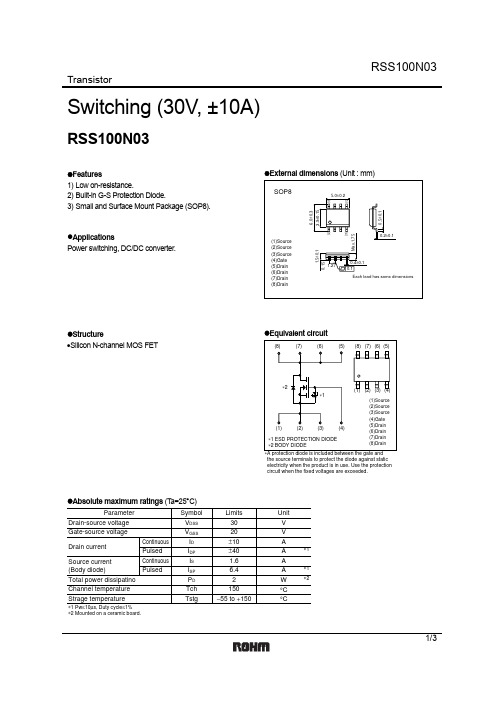
Transistor1/3Switching (30V, ±10A)RSS100N03z Features1) Low on-resistance.2) Built-in G-S Protection Diode.3) Small and Surface Mount Package (SOP8).z ApplicationsPower switching, DC/DC converter.z External dimensions (Unit : mm)z Structure•Silicon N-channel MOS FET z Equivalent circuitthe source terminals to protect the diode against static electricity when the product is in use. Use the protection circuit when the fixed voltages are exceeded.z Absolute maximum ratings (T a=25°C)∗1∗1∗2ParameterV V DSS Symbol 30V V GSS 20A I D ±10A I DP ±40A I S 1.6A I SP 6.4W P D 2°C Tch 150°CTstg −55 to +150Limits Unit Drain-source voltage Gate-source voltage Drain current Total power dissipatino Channel temperature Strage temperatureContinuous Pulsed Continuous Source current (Body diode)Pulsed∗1 Pw ≤10µs, Duty cycle ≤1%∗2 Mounted on a ceramic board.Transistor2/3z Thermal resistance (T a=25°C)°C / WRth (ch-a)62.5ParameterSymbol Limits Unit Channel to ambient∗ Mounted on a ceramic board.∗z Electrical characteristics (T a=25°C)z Body diode characteristics (Source-Drain Characteristics) (T a=25°C)Forward voltageV SD −− 1.2V I S=6.4A, V GS =0VParameterSymbol Min.Typ.Max.Unit Conditions∗Pulsed∗z Electrical characteristic curvesDRAIN-SOURCE VOLTAGE : V DS (V)C A P A C I T A N C E : C (p F )Fig.1 Typical Capacitancevs. Drain-Source VoltageDRAIN CURRENT : I D (A)S W I T C H I N G T I M E : t (n s )Fig.2 Switching CharacteristicsTOTAL GATE CHARGE : Qg (nC)G A T E -S O U R C E V O L T A G E : V G S (V )Fig.3 Dynamic Input CharacteristicsTransistor3/3GATE-SOURCE VOLTAGE : V GS (V)D R A I N C U R RE N T : I D (A )Fig.4 Typical Transfer CharacteristicsGATE-SOURCE VOLTAGE : V GS (V)S T A T I C D R A I N -S O U R C E O N -S T A T E R E S I S T A N C E : R D S (o n ) (m Ω)Fig.5 Static Drain-SourceOn-State Resistance vs. Gate-Source VoltageSOURCE-DRAIN VOLTAGE : V SD (V)S O U R C E C U R R E N T : I s (A )Fig.6 Source Current vs.Source-Drain VoltageDRAIN CURRENT : I D (A)1101001000S T A T I C D R A I N -S O U R C E O N -S T A T E R E S I S TA N C E : R D S (o n ) (m Ω)Fig.7 Static Drain-SourceOn-State Resistance vs. Drain Current (Ι)DRAIN CURRENT : I D (A)S T A T I C D R A I N -S O U R C E O N -S T A T E R E S I S T A N C E : R D S (o n ) (m Ω)Fig.8 Static Drain-SourceOn-State Resistance vs. Drain Current (ΙΙ)DRAIN CURRENT : I D (A)S T A T I C D R A I N -S O U R C E O N -S T A T E R E S I S T A N C E : R D S (o n ) (m Ω)Fig.9 Static Drain-SourceOn-State Resistance vs. Drain Current (ΙΙΙ)AppendixAbout Export Control Order in JapanProducts described herein are the objects of controlled goods in Annex 1 (Item 16) of Export Trade ControlOrder in Japan.In case of export from Japan, please confirm if it applies to "objective" criteria or an "informed" (by MITI clause)on the basis of "catch all controls for Non-Proliferation of Weapons of Mass Destruction.Appendix1-Rev1.0。
诺瓦科技LED显示屏联网播放器T3规格书英文版

Taurus SeriesMultimedia PlayersT3 SpecificationsProduct Version: V1.3.0 Document Number:NS120100242XI 'AN NOVA ST A R TEC H C O .,L T D .Copyright © 2018 Xi’an NovaStar Tech Co., Ltd. All Rights Reserved.No part of this document may be copied, reproduced, extracted or transmitted in any form or by any means without the prior written consent of Xi’an Nova Star Tech Co., Ltd.Trademarkis a trademark of Xi’an NovaStar Tech Co., Ltd.StatementYou are welcome to use the product of Xi’an NovaStar Tech Co., Ltd. (hereinafter referred to as NovaStar). This document is intended to help you understand and use the product. For accuracy and reliability, NovaStar may make improvements and/or changes to this document at any time and without notice. If you experience any problems in use or have any suggestions, please contact us via contact info given in document. We will do our best to solve any issues, as well as evaluate and implement any suggestions.X I'A NN OV AS TA RT EC HC O.,L TD.Table of ContentsTable of Contents ............................................................................................................................ ii 1 Safety .. (1)1.1 Storage and Transport Safety ..................................................................................................................... 1 1.2 Installation and Use Safety .. (1)2 Overview (3)2.1 Introduction .................................................................................................................................................. 3 2.2 Application ................................................................................................................................................... 3 3 Features ........................................................................................................................................... 5 3.1 Synchronization mechanism for multi-screen playing ................................................................................. 5 3.2 Powerful Processing Capability ................................................................................................................... 5 3.3 Omnidirectional Control Plan .. (5)3.4 Dual-Wi-Fi Mode .......................................................................................................................................... 6 3.4.1 Wi-Fi AP Mode .......................................................................................................................................... 7 3.4.2 Wi-Fi Sta Mode .. (7)3.4.3 Wi-Fi AP+Sta Mode .................................................................................................................................. 7 3.5 Redundant Backup ...................................................................................................................................... 8 4 Hardware Structure....................................................................................................................... 9 4.1 Appearance . (9)4.2 Dimensions (11)5 Software Structure (12)5.1 System Software ........................................................................................................................................ 12 5.2 Related Configuration Software .. (12)6 Product Specifications ................................................................................................................ 13 7 Audio and Video Decoder Specifications (15)7.1 Image ......................................................................................................................................................... 15 7.1.1 Decoder .................................................................................................................................................. 15 7.1.2 Encoder .................................................................................................................................................. 15 7.2 Audio .......................................................................................................................................................... 16 7.2.1 Decoder .. (16)X I 'A N N O V A S T A R T E C H C O .,L T D.7.2.2 Encoder (16)7.3 Video (17)7.3.1 Decoder (17)7.3.2 Encoder (18)X I'A NN OV AS TA RT EC HC O.,L TD.1SafetyThis chapter illustrates Taurus series products safety to ensure storage, transportation, installation and usage safety of the products.Safety description is applicable to all personnel that contact or use the products. First, pay attention to following points:● Read throughout the description. ● Save the whole description.●Be complied with the whole description.1.1 Storage and Transport Safety ● Pay attention to dust and water prevention.● Avoid long-term direct sunlight. ● Do not place the products in the position near fire and heat.● Do not place the products in an area containing explosive materials. ● Do not place the products in strong electromagnetic environment. ● Place the products in a stable position to prevent damage or personal injury caused by dropping.●Save the packing box and materials which will come in handy if you ever have to ship your products. For maximum protection, repack your product as it wasoriginally packed at the factory.1.2 Installation and Use Safety● Only trained professionals may install the products.● Do not insert and unplug (power cord plug) when the power is on. ● Ensure the safe grounding of the device.● Be careful about electric shock risk. Built-in power supply. ● Always wear a wrist band and insulating gloves.● Do not place the products in an area having more or strong shake. ● Perform dust removing regularly.●Rather than having the product disassembled and maintained by non-certified professionals, please contact NovaStar for maintenance at any time.X I 'A N N O V A S T A R T E CHCO .,L T D.Replace faulty parts only with the spare parts supplied by NovaStar.X I'A NN OV AS TA RT EC HC O.,L TD.2Overview2.1 IntroductionTaurus series products are NovaStar's second generation of multimedia players dedicated to small and medium-sized full-color LED displays.T3 of the Taurus series products (herein after referred to as “T 3”) feature following advantages, better satisfying users’ requir ements:●Loading capacity up to 650,000 pixels●Synchronization mechanism for multi-screen playing● Powerful processing capability ● Omnidirectional control plan ● Dual-Wi-Fi mode ●Redundant backup Note: If the user has a high demand on synchronization, the time synchronization module isrecommended. For details, please consult our technical staff. In addition to solution publishing and screen control via PC, mobile phones and LAN, the omnidirectional control plan also supports remote centralized publishing and monitoring. 2.2 ApplicationTaurus series products can be widely used in LED commercial display field, such asbar screen, chain store screen, advertising machine, mirror screen, retail store screen, door head screen, on board screen and the screen requiring no PC. Classification of Taurus’ application cases is shown in Table 2-1. Table 2-1 ApplicationXI 'A N N O V A S T A R T E C H C O .,L T D.X I'A NN OV AS TA RT EC HC O.,L T3Features3.1 Synchronization mechanism for multi-screen playingThe T3 support switching on/off function of synchronous display.When synchronous display is enabled, the same content can be played on different displays synchronously if the time of different T3 units are synchronous with one another and the same solution is being played.3.2 Powerful Processing CapabilityThe T3 feature powerful hardware processing capability: ● 1.5 GHz eight-core processor●Support for H.265 4K high-definition video hardware decoding playback ● Support for 1080P video hardware decoding ● 2 GB operating memory●8 GB on-board internal storage space with 4 GB available for users 3.3 Omnidirectional Control Plan Table 3-1 Control PlanXI 'A N N O V A S T A R T E C H CO .,L T D.Cluster control plan is a new internet control plan featuring following advantages:●More efficient: Use the cloud service mode to process services through a uniformplatform. For example, VNNOX is used to edit and publish solutions, and NovaiCare is used to centrally monitor display status.● More reliable: Ensure the reliability based on active and standby disaster recovery mechanism and data backup mechanism of the server. ● More safe: Ensure the system safety through channel encryption, data fingerprintand permission management. ● Easier to use: VNNOX and NovaiCare can be accessed through Web. As long asthere is internet, operation can be performed anytime and anywhere. ●More effective: This mode is more suitable for the commercial mode of advertising industry and digital signage industry, and makes information spreading more effective. 3.4 Dual-Wi-Fi Mode The T3 have permanent Wi-Fi AP and support the Wi-Fi Sta mode, carryingadvantages as shown below:●Completely cover Wi-Fi connection scene. The T3 can be connected to through self-carried Wi-Fi AP or the external router.●Completely cover client terminals. Mobile phone, Pad and PC can be used to log in T3 through wireless network.●Require no wiring. Display management can be managed at any time, having improvements in efficiency.T3’s Wi -Fi AP signal strength is related to the transmit distance and environment. Users can change the Wi-Fi antenna as required.XI 'A NN O V A S T A R T E C H C O .,L T D3.4.1 Wi-Fi AP ModeUsers connect the Wi-Fi AP of a T3 to directly access the T3. The SSID is “AP + the last 8 digits of the SN ”, for example, “AP10000033”, and the default password is “12345678”.3.4.2 Wi-Fi Sta Mode Configure an external router for a T3 and users can access the T3 by connecting the external router. If an external router is configured for multiple T3 units, a LAN can becreated. Users can access any of the T3 via the LAN.3.4.3 Wi-Fi AP+Sta ModeIn Wi-Fi AP+ Sta connection mode, users can either directly access the T3 or accessinternet through bridging connection. Upon the cluster solution, VNNOX andNovaiCare can realize remote solution publishing and remote monitoring respectively through the Internet.XI 'A N N O V A S T A R T E C HCO .,L T D.3.5 Redundant BackupT3 support network redundant backup and Ethernet port redundant backup.●Network redundant backup: The T3 automatically selects internet connectionmode among wired network or Wi-Fi Sta network according to the priority.●Ethernet port redundant backup: The T3 enhances connection reliability throughactive and standby redundant mechanism for the Ethernet port used to connectwith the receiving card.X I'A NN OV AS TA RT EC HC O.,L TD.4Hardware Structure4.1 AppearanceFigure 4-1 Appearance of T3Note: Product images provided in this file are for reference only, and the actualproducts shall prevail.Table 4-1 Connectors and buttons of the T3XI 'AN NOVA S TAR T E C HCO .,L T D.Note: Product images provided in this file are for reference only, and the actual products shall prevail.Table 4-2 Indicators of the T3 A R T E C HCO .,L T D.4.2 DimensionsThe total thickness (board thickness + thickness of the components on the front andback side) is no greater than 25.0mm.Unit of the dimension chart is “mm”. Ground connection is enabled for location hole(GND).X I'A NN OV AS TA RT EC HC O.,L TD.5Software Structure5.1 System Software● Android operating system software ● Android terminal application software ●FPGA programNote: The third-party applications are not supported.5.2 Related Configuration SoftwareTable 5-1 Related configuration softwareE C HCO .,L T D.6 Product Specifications SpecificationsAntennaAntenna extension mastX I'A NN OV AS TA RT EC HC O.,L TD.7Audio and Video DecoderSpecifications7.1 Image7.1.1 Decoder7.1.2 EncoderO .,L T D.7.2 Audio 7.2.1 Decoder7.2.2 Encoder7.3 Video 7.3.1 DecoderNote: Output data format is YUV420 semi-planar, and YUV400(monochrome) is also supported for H.264.7.3.2 EncoderXI 'AN NOVA S。
- 1、下载文档前请自行甄别文档内容的完整性,平台不提供额外的编辑、内容补充、找答案等附加服务。
- 2、"仅部分预览"的文档,不可在线预览部分如存在完整性等问题,可反馈申请退款(可完整预览的文档不适用该条件!)。
- 3、如文档侵犯您的权益,请联系客服反馈,我们会尽快为您处理(人工客服工作时间:9:00-18:30)。
P-TO252-3-11P-TO251-3-11IPD03N03LA G IPS03N03LA GParameterSymbol ConditionsUnitmin.typ.max.Thermal characteristicsThermal resistance, junction - case R thJC -- 1.3K/WSMD version, device on PCBR thJAminimal footprint --756 cm 2 cooling area 5)--50Electrical characteristics, at T j =25 °C, unless otherwise specified Static characteristicsDrain-source breakdown voltage V (BR)DSS V GS =0 V, I D =1 mA 25--VGate threshold voltage V GS(th)V DS =V GS , I D =70 µA 1.2 1.62Zero gate voltage drain currentI DSSV DS =25 V, V GS =0 V, T j =25 °C-0.11µA V DS =25 V, V GS =0 V, T j =125 °C-10100Gate-source leakage current I GSS V GS =20 V, V DS =0 V -10100nA Drain-source on-state resistanceR DS(on)V GS =4.5 V, I D =60 A - 4.3 5.3m ΩV GS =4.5 V, I D =60 A, SMD version - 4.1 5.1V GS =10 V, I D =60 A - 2.9 3.4V GS =10 V, I D =60 A, SMD version- 2.7 3.2Gate resistance R G - 1.3-ΩTransconductanceg fs|V DS |>2|I D |R DS(on)max , I D =60 A56113-S 5)Device on 40 mm x 40 mm x 1.5 mm epoxy PCB FR4 with 6 cm 2(one layer, 70 µm thick) copper area for drain connection. PCB is vertical in still air.Values 1)Current is limited by bondwire; with an R thJC =1.3 K/W the chip is able to carry 142 A.3)See figure 34) T j,max =150 °C and duty cycle D <0.25 for V GS <-5 V1)J-STD20 and JESD22IPD03N03LA G IPS03N03LA GParameter Symbol Conditions Unitmin.typ.max. Dynamic characteristicsInput capacitance C iss-39005200pF Output capacitance C oss-15002000 Reverse transfer capacitance C rss-170260Turn-on delay time t d(on)-1319ns Rise time t r-1015Turn-off delay time t d(off)-4262Fall time t f- 6.610Gate Charge Characteristics6)Gate to source charge Q gs-1217nC Gate charge at threshold Q g(th)- 6.38.3Gate to drain charge Q gd-8.613 Switching charge Q sw-1521Gate charge total Q g-3141Gate plateau voltage V plateau- 3.2-VGate charge total, sync. FET Q g(sync)V DS=0.1 V,V GS=0 to 5 V-2837nCOutput charge Q oss V DD=15 V, V GS=0 V-3243 Reverse DiodeDiode continous forward current I S--90A Diode pulse current I S,pulse--360Diode forward voltage V SD V GS=0 V, I F=90 A,T j=25 °C-0.92 1.2VReverse recovery charge Q rr V R=15 V, I F=I S,d i F/d t=400 A/µs--20nC6) See figure 16 for gate charge parameter definition T C=25 °CValuesV GS=0 V, V DS=15 V,f=1 MHzV DD=15 V, V GS=10 V,I D=25 A, R G=2.7 ΩV DD=15 V, I D=45 A,V GS=0 to 5 V5 Typ. output characteristics1 Power dissipation9 Drain-source on-state resistance13 Avalanche characteristicsIPD03N03LA G IPS03N03LA G Package OutlineP-TO252-3-11: OutlineFootprint:Packaging:Dimensions in mmIPD03N03LA G IPS03N03LA G Published byInfineon Technologies AGBereich KommunikationSt.-Martin-Straße 53D-81541 München© Infineon Technologies AG 1999All Rights Reserved.Attention please!The information herein is given to describe certain components and shall not be considered aswarranted characteristics.Terms of delivery and rights to technical change reserved.We hereby disclaim any and all warranties, including but not limited to warranties of non-infringement, regarding circuits, descriptions and charts stated herein.Infineon Technologies is an approved CECC manufacturer.InformationFor further information on technology, delivery terms and conditions and prices, please contact your nearest Infineon Technologies office in Germany or our Infineon Technologies representatives worldwide (see address list).WarningsDue to technical requirements, components may contain dangerous substances.For information on the types in question, please contact your nearest Infineon Technologies office. Infineon Technologies' components may only be used in life-support devices or systems with the expressed written approval of Infineon Technologies if a failure of such components can reasonablybe expected to cause the failure of that life-support device or system, or to affect the safety or effectiveness of that device or system. Life support devices or systems are intended to be implantedin the human body, or to support and/or maintain and sustain and/or protect human life. If they fail,it is reasonable to assume that the health of the user or other persons may be endangered.。