eMwin 移植 文档飞利浦 恩智浦
mcu移植流程范文

mcu移植流程范文MCU(Microcontroller Unit)是一种微型计算机系统,包含了CPU、存储器、输入输出接口和定时器等部件,广泛应用于各种嵌入式系统中。
MCU移植指的是将相同或不同架构的MCU芯片上的软件移植到另一种MCU芯片上的过程,以便在新的硬件平台上运行软件。
这篇文章将详细介绍MCU移植的流程。
1.硬件平台选型:首先需要选择目标MCU芯片,确保该芯片具备满足项目需求的功能特性。
考虑芯片的处理能力、存储容量、外设接口、功耗等因素。
同时,要注意MCU是否支持所需的移植操作系统或开发环境。
2.准备开发环境:根据目标MCU芯片的选择,安装相应的集成开发环境(IDE)和编译器。
这些开发工具通常由MCU芯片厂商提供,用于编写、编译和调试软件。
3.移植操作系统:如果移植的软件涉及到操作系统,需要进行操作系统的移植。
首先,要了解目标MCU芯片支持的操作系统类型,比如RTOS(实时操作系统)或者Linux,然后将操作系统的源代码和配置文件导入到开发环境中,并进行编译和调试。
4.移植设备驱动程序:设备驱动程序是控制外围设备的软件模块,如串口、GPIO、ADC等。
将原有设备驱动程序的源代码导入到开发环境中,并进行适配和调试,确保其与目标MCU芯片的硬件接口兼容。
5.移植应用程序:将原有应用程序的源代码导入到开发环境中,并进行编译和调试。
由于不同MCU芯片的指令集、存储器布局等可能有所差异,需根据目标MCU 的特性进行相应的修改和优化。
6.端口移植:一些软件可能依赖于特定的硬件平台或外部库,需要进行端口移植。
比如,涉及具体的硬件操作的代码或与外部库的接口等,需根据目标MCU 的硬件平台特点进行修改。
7.调试和测试:完成移植后,需要进行软件的调试和测试,确保软件在目标MCU芯片上能够正常工作。
可以使用调试工具和仿真器对程序进行单步执行和观察内部状态,以及通过外设接口验证软件功能。
8.性能优化:在软件运行过程中,可能会出现性能瓶颈或资源浪费的问题。
NXP恩智浦 Freescale飞思卡尔后你需要知道的十件事

NXP恩智浦Freescale飞思卡尔后你需要知道的十件事这两年,半导体行业似乎进入了多事之秋,收购战此起彼伏。
就在今年短短的3个月里,半导体行业并/收购案有:Avago Technologies 以6 亿美金价格收购无线网络公司Emulex Corp ELX.O,Maxlinear以2.87亿美元收购Entropic Communications,Lattice半导体则将以6亿美元价格收购Silicon Image。
3月初,恩智浦(NXP)以约118亿美元的价格并购飞思卡尔(Freescale),合并后的企业价值将超过400亿美元。
大公司的收购往往错综复杂,他们也有自己难以取舍的地方,有经济、情感、形象等多方面的考量。
这次并购会对恩智浦和飞思卡尔各自的产品、目标行业、半导体产业以及竞争对手带来哪些影响呢?我们目前还不能得到准确答案,但是希望能从对两家公司的十大对比中,让你看出一些端倪。
1.优势产品恩智浦微控制器、射频、传感器、无线(NFC)、模拟及电源。
杀手锏:NFC、智能卡IC。
飞思卡尔MCU&通信处理器、模拟技术与电源管理、射频、无线连接、传感器、软件和开发工具。
杀手锏:MCU&通信处理器(ARM MCU、ARM 应用处理器、QorIQ多核处理器、Power处理器、DSP)。
恩智浦+ 飞思卡尔不难发现,这两家的产品互补性很强,一个擅长连接,一个擅长处理和控制连接及其带来的数据。
恩智浦和飞思卡尔的专利数都约为10 000,可以从一个侧面反映他们的势均力敌。
而下面的专利“地图”,会让你直接感受到他们各自的强项。
图1 恩智浦与飞思卡尔的专利“地图” 在宣布合并交易时,恩智浦表示将出售自家高性能RF产品部门以避免主管机关审查问题,其实是因为NXP将保留原属于飞思卡尔、技术实力更强的RF部门,而不是他们自己的。
如果两家公司的RF业务合并,将有垄断全球高性能RF市场之虞,美国与欧洲的反垄断机构以及中国的商务部将审查这项合并交易。
移植文档

uCOS-II+LwIP的应用 LwIP终于能跑了,总结下: 平台是LPC2136+ENC28J60,32K的RAM,软件是uCOS-II 2.51+LwIP 1.1.1。 感觉主要解决两个问题: 操作系统仿真层的移植。这个基于uCOS-II的代码太多了。COPY下就行! 1,设备驱动的移植. 驱动的移植主要就是完成ethernetif.c的工作。作者已经给好了驱动的接口。
Net_if.h -----------------86; struct netif { struct netif *next; struct ip_addr ip_addr; struct ip_addr netmask; struct ip_addr gw; err_t (* input)(struct pbuf *p, struct netif *inp); err_t (* output)(struct netif *netif, struct pbuf *p, struct ip_addr *ipaddr); err_t (* linkoutput)(struct netif *netif, struct pbuf *p); void *state; #if LWIP_DHCP struct dhcp *dhcp; #endif unsigned char hwaddr_len; unsigned char hwaddr[NETIF_MAX_HWADDR_LEN]; u16_t mtu; char name[2]; u8_t num; u8_t flags; }; 主要就是: err_t (* input)(struct pbuf *p, struct netif *inp); 这个是被驱动调用的,传递一个数据包给TCP/IP栈。 err_t (* output)(struct netif *netif, struct pbuf *p,struct ip_addr *ipaddr); 这个是被IP模块调用的,向以太网上发送一个数据包,函数要先通过IP地址获得解决硬件地址,然后发包。 err_t (* linkoutput)(struct netif *netif, struct pbuf *p); 这个是直接发送数据包的接口。
恩智浦S32R274汽车雷达处理器应用指南说明书
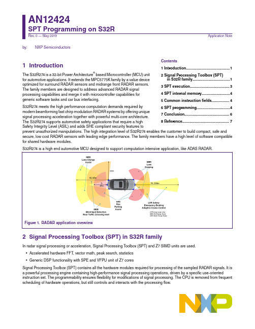
by:NXP Semiconductors1Introduction The S32R274 is a 32-bit Power Architecture ® based Microcontroller (MCU) unitfor automotive applications. It extends the MPC5775K family by a value deviceoptimized for surround RADAR sensors and midrange front RADAR sensors.The family members are designed to address advanced RADAR signalprocessing capabilities and merge it with microcontroller capabilities forgeneric software tasks and car bus interfacing.S32R274 meets the high performance computation demands required by modern beamforming fast chirp modulation RADAR systems by offering unique signal processing acceleration together with powerful multi-core architecture.The S32R274 supports automotive safety applications that require a highSafety Integrity Level (ASIL) and adds SHE compliant security features toprevent unauthorized manipulations. The high integration level of S32R274 enables the customer to build compact, safe and secure, low cost RADAR sensors with leading edge performance. The family members have a high level of software compatible for shared hardware modules.S32R274 is a high end automotive MCU designed to support computation intensive application, like ADAS RADAR.Figure 1.RADAR application overview2Signal Processing Toolbox (SPT) in S32R familyIn radar signal processing or acceleration, Signal Processing T oolbox (SPT) and Z7 SIMD units are used.•Accelerated hardware FFT , vector math, peak search, statistics•Generic DSP functionality with SPE and VFPU unit of Z7 coresSignal Processing T oolbox (SPT) contains all the hardware modules required for processing of the sampled RADAR signals. It is a powerful processing engine containing high-performance signal processing operations, driven by a specific use-orientedinstruction set. The programmability ensures flexibility for modifications of signal processing. The CPU is removed from frequent scheduling of hardware operations, but still controls and interacts with the processing flow.Contents1 Introduction (1)2 Signal Processing Toolbox (SPT)in S32R family....................................13 SPT execution......................................34 SPT internal memory...........................45 Common instruction fields.................46 SPT programming................................47 Conclusion. (6)8 Reference.............................................7AN12424SPT Programming on S32R Rev. 0 — May 2019Application NoteSPT is connected to the device by an advanced high performance master bus and a peripheral bus.Figure 2.SPT in S32R274 block diagramThe system bus master interface performs fast data transfers between external memory and local RAM.The purpose of the peripheral interface is to set configuration, get status information and basic control of SPT (start/stop, program pointer) and to trigger interrupts. It can also be used to exchange small amounts of the data between the CPU and the SPT , such as constant operands.Figure 3.SPT block diagramIt has the following features:•Acquisition of ADC samples—Capturing of ADC samples within programmed window—On-the-fly statistical computation—Supports MIPICSI2 interface•Provides HW acceleration for—FFT (8 - 4096 point)—Histogram calculation—Maximum and peak searchSignal Processing Toolbox (SPT) in S32R family—Mathematical operations on vector data•High-speed DMA data transfer—Supports system RAM, TCM and Flash memory transfers—Includes compression/decompression capability for reduction of storage footprint•Instruction based program flow—High-level commands for signal processing operations—Simple control commands—Local instruction buffer—Automatic instruction fetch from main memory—CPU interaction possible•CPU interruption notification•Watchdog•Debug Support - Single Stepping and Jamming ModeIt has three operation modes:1.STOP mode2.System Debug mode3.Normal mode3SPT executionThe SPT executes a list of instructions. These commands contain all the information to perform signal processing operations on data vectors consisting of a set of numbers. The instruction list is provided by the CPU in a memory buffer (SRAM or flash) and read by the SPT with autonomous triggered DMA operations. Preparation of command scripts is performed off-line duringdevelopment on a different system, such as a PC.Figure 4.SPT operation modelData as results or inputs of signal processing operations can be transferred between operand/twiddle RAM and system RAM or TCM by DMA operations. These kind of DMA operations are also scheduled by commands in the script.CPU application software functions may be invoked between signal processing operations. In order to synchronize these SW functions with the processing flow, interrupts and polling flags are provided, which may be activated as a result of specificcommands. In the same way, eDMA operations can be triggered from the SPT . The data transfer descriptors need to be prepared by application software.T o enable advanced and precisely timed pipelining of HW assisted operations, SPT command execution can also be synchronized with or triggered by events from CTE or MIPICSI2.SPT executionSPT internal memoryProgram execution is performed by a dedicated register machine. The program execution may be stalled at the end of each command and can be synchronized with events provided by the CTE or MIPICSI2. The CPU can stop and release program execution and execute its own instructions in the same time.The SPT command sequence is provided by CPU SW and written to a buffer in the system RAM or flash, where CSDMA fetches or alternatively transfers the list of instructions to the command queue.The program is executed sequentially, one command following the next in the chain with the exception being loops and asynchronous PDMA instruction. The end of a sequence is marked with a specific termination command. The start address of the instruction sequence is configured by application software using the peripheral interface.The command queue stores a number of instructions to be executed, which may be a shorter sequence than the complete instruction list. It maintains an instruction pointer to the current executed operation, which is incremented when the current operation is completed. This instruction pointer indicates the position in the complete instruction list sequence relative to the first instruction.Loop instructions are special cases, the program sequence may continue with a lower address depending on the state of the loop counter. The start and next command address of the loops are saved in special registers. Up to four nested loops are supported. Jump instructions or branch instructions are another case where the program may cause the program to branch to a non-contiguous address location. It is the responsibility of the assembler to ensure that the sanity of the program structure is not violated i.e. infinite loops, jumping into or out of a loop, etc.4SPT internal memorySPT contains internal memory resources namely, Operand RAM, Twiddle RAM and work registers. Out of these, only the work registers can be directly accessed via the peripheral interface and are visible on the SPT external memory map.The CPU can access these internal memory resources via the hardware accelerators. The instruction bitfields SRC_ADD and DEST_ADD point to these memories.The Twiddle RAM extends from location 0x4000 to 0x4FFF. However the area from 0x5000 to 0x7FFF is aliased to the Twiddle RAM i.e. it wraps around to point to the T widdle RAM. It should be noted that the memory accesses to the T widdle RAM should not cross the area from 0x4000 to 0x7FFF.The Operand RAM extends from location 0x8000 to 0xBFFF. But the area from 0xC000 to 0xFFFF is aliased to the Operand RAM. The memory accesses to the Operand RAM should not cross the area from 0x8000 to 0xFFFF.5Common instruction fieldsCommon instructions contains the following fields.•Opcode•Source and Destination address•Indirect Memory address•Source and destination address increment•Vector size•Input datatype/preprocessing6SPT programming6.1Programming based on RSDKNXP Radar SDK(RSDK) provides basic radar processing algorithms and device drivers for S32R hardware devices. Its purpose is to facilitate radar algorithm development (using SPT kernels, MA TLAB models), creation of higher level algorithms (starting from the basic blocks supplied with RSDK) and easy application development by integrating driver and platform support.Radar SDK (Radar SDK for S32R27 SPT accelerator ) could be downloaded from NXP website.RSDK SPT module consists of the SPT Driver, SPT Kernels software components.The SPT Driver serves as an interface between the user application running on the host CPU cores and the SPT hardware. The figure below shows a high-level block diagram of SPT software architecture. Its purpose is to enable the integration and executionof low-level microcode kernels on the SPT (Signal Processing T oolbox) accelerator for baseband radar signal processing.Figure 5.SPT software architectureThe SPT Kernels are individual precompiled routines of SPT code packed into a library, each implementing a part of the radar processing flow.T ogether, the SPT Driver and SPT Kernels library provide a software abstraction of the built-in SPT hardware functions (e.g. FFT ,Maximum Search, Histogram etc.) combined in a series of algorithms.The RSDK package also includes RSDK Sample Applications showing how to integrate these software components into the user code.6.2Programming based on graphic toolS32 Design Studio SPT graphical tool allows user to use graphical modeling workbench by leveraging the Eclipse Modeling technologies. It provides a workbench for model-based architecture engineering. Graphical tool equips teams who have to deal with complex architectures. The graphical tool includes everything necessary to easily create and manipulate models. The output of this tool is SPT assembler source code.The SPT graphical tool is integrated with the New S32DS Project wizard for devices which have SPT module. SPT1, SPT2 and SPT2.5 versions of SPT modules are supported. The SPT graphical tool can be used after project creation with the new graph tools project wizard. For detailed description of new project wizards, please read S32 Design Studio for Power Architecture, Version 2017.R1 reference manual.After the project is generated, SPT graphical tool windows could be gotten in IDE. User could drag 'Instructions', 'Flow' and 'Directives' from Palette window into working flow window.SPT programmingEach 'Instructions', 'Flow' or 'Directives' could change their setting in properties window. After finished the design of SPT working flow, generate SPT code through right click mouse.Figure 6.Generate project with SPT graphical toolFigure 7.SPT graphical tool windowsFigure 8.Example working flow and generate code7ConclusionThe SPT is a powerful processing engine containing high-performance signal processing operations driven by a specific instruction set. Its programmability ensures flexibility while removing the CPU from frequent scheduling of hardware operations, while still controlling and interacting with the processing flow. RSDK supports the API of SPT for customer and graphics tool for SPT programming could meet the flexible design request.8Reference•S32R274 Reference Manual•Radar SDK for S32R27 SPT accelerator •AN5375, S32R RADAR Signal CompressionHow To Reach Us Home Page: Web Support: /support Information in this document is provided solely to enable system and software implementers to use NXP products. There are no express or implied copyright licenses granted hereunder to design or fabricate any integrated circuits based on the information in this document. NXP reserves the right to make changes without further notice to any products herein.NXP makes no warranty, representation, or guarantee regarding the suitability of its products for any particular purpose, nor does NXP assume any liability arising out of the application or use of any product or circuit, and specifically disclaims any and all liability, including without limitation consequential or incidental damages. “Typical” parameters that may be provided in NXP data sheets and/or specifications can and do vary in different applications, and actual performance may vary over time. All operating parameters, including “typicals,” must be validated for each customer application by customer's technical experts. NXP does not convey any license under its patent rights nor the rights of others. NXP sells products pursuant to standard terms and conditions of sale, which can be found at the following address: / SalesTermsandConditions.While NXP has implemented advanced security features, all products may be subject to unidentified vulnerabilities. Customers are responsible for the design and operation of their applications and products to reduce the effect of these vulnerabilities on customer’s applications and products, and NXP accepts no liability for any vulnerability that is discovered. Customers should implement appropriate design and operating safeguards to minimize the risks associated with their applications and products.NXP, the NXP logo, NXP SECURE CONNECTIONS FOR A SMARTER WORLD, COOLFLUX, EMBRACE, GREENCHIP, HIT AG, I2C BUS, ICODE, JCOP, LIFE VIBES, MIFARE, MIFARE CLASSIC, MIFARE DESFire, MIFARE PLUS, MIFARE FLEX, MANTIS, MIFARE ULTRALIGHT, MIFARE4MOBILE, MIGLO, NTAG, ROADLINK, SMARTLX, SMARTMX, ST ARPLUG, TOPFET, TRENCHMOS, UCODE, Freescale, the Freescale logo, AltiVec, C‑5, CodeTEST, CodeWarrior, ColdFire, ColdFire+, C‑Ware, the Energy Efficient Solutions logo, Kinetis, Layerscape, MagniV, mobileGT, PEG, PowerQUICC, Processor Expert, QorIQ, QorIQ Qonverge, Ready Play, SafeAssure, the SafeAssure logo, StarCore, Symphony, VortiQa, Vybrid, Airfast, BeeKit, BeeStack, CoreNet, Flexis, MXC, Platform in a Package, QUICC Engine, SMARTMOS, Tower, TurboLink, and UMEMS are trademarks of NXP B.V. All other product or service names are the property of their respective owners. AMBA, Arm, Arm7, Arm7TDMI, Arm9, Arm11, Artisan, big.LITTLE, Cordio, CoreLink, CoreSight, Cortex, DesignStart, DynamIQ, Jazelle, Keil, Mali, Mbed, Mbed Enabled, NEON, POP, RealView, SecurCore, Socrates, Thumb, TrustZone, ULINK, ULINK2, ULINK-ME, ULINK-PLUS, ULINKpro, µVision, Versatile are trademarks or registered trademarks of Arm Limited (or its subsidiaries) in the US and/or elsewhere. The related technology may be protected by any or all of patents, copyrights, designs and trade secrets. All rights reserved. Oracle and Java are registered trademarks of Oracle and/or its affiliates. The Power Architecture and word marks and the Power and logos and related marks are trademarks and service marks licensed by .© NXP B.V. 2019.All rights reserved.For more information, please visit: Forsalesofficeaddresses,pleasesendanemailto:**********************Date of release: May 2019Document identifier: AN12424。
ZYNQFLASH+EMMC手动移植LINUX启动

ZYNQFLASH+EMMC⼿动移植LINUX启动前⾔虽可使⽤Petalinux进⾏移植,简单⽅便,但为了更清楚明⽩的了解整个流程,还是尝试了⼀波⼿动移植。
参考资料流程对于⼿动移植,所需的⽂件为:BOOT.bin(FSBL+fpga_bit⽂件+u_boot.elf)、uImage、devicetree.dtb、uEnv.txt、⽂件系统⽂件放置位置说明:FLASH:BOOT.bin(FSBL+fpga_bit⽂件+u_boot.elf)EMMC:第⼀个分区放置:uImage、devicetree.dtb、uEnv.txt第⼆个分区放置:⽂件系统启动流程为:板⼦设置为QSPI启动模式,FSBL执⾏调u-boot执⾏,u-boot根据uEnv.txt调EMMC分区1中的内核执⾏,内核最后跳到分区⼆中的⽂件系统。
FSBL、bit⽂件、uImage、⽂件系统都可复⽤SD卡移植模式下的内容:参考参考资料第⼀个链接。
本⽂章主要讲述的重点在于:u-boot、设备树、uEnv.txt的更改部分板⼦主要信息说明:板⼦芯⽚:ZYNQ7035,板⼦的调试打印串⼝为PS0,板⼦上有SD卡(SD0)、EMMC(SD1),板⼦上有FLASH。
其他外设不赘述。
u-boot移植说明:NOTE:u-boot xilinx-v2018.3版本的zynq-common.h跟xilinx-v2018.1版本的不⼀样,这⾥检出v2018.1版本使⽤。
主要是CONFIG_EXTRA_ENV_SETTINGS环境变量不⼀致。
默认的如下所⽰:/* Default environment */#ifndef CONFIG_EXTRA_ENV_SETTINGS#define CONFIG_EXTRA_ENV_SETTINGS \"ethaddr=00:0a:35:00:01:22\0" \"kernel_image=uImage\0" \"kernel_load_address=0x2080000\0" \"ramdisk_image=uramdisk.image.gz\0" \"ramdisk_load_address=0x4000000\0" \"devicetree_image=devicetree.dtb\0" \"devicetree_load_address=0x2000000\0" \"bitstream_image=system.bit.bin\0" \"boot_image=BOOT.bin\0" \"loadbit_addr=0x100000\0" \"loadbootenv_addr=0x2000000\0" \"kernel_size=0x500000\0" \"devicetree_size=0x20000\0" \"ramdisk_size=0x5E0000\0" \"boot_size=0xF00000\0" \"fdt_high=0x20000000\0" \"initrd_high=0x20000000\0" \"bootenv=uEnv.txt\0" \"loadbootenv=load mmc 0 ${loadbootenv_addr} ${bootenv}\0" \"importbootenv=echo Importing environment from SD ...; " \"env import -t ${loadbootenv_addr} $filesize\0" \"sd_uEnvtxt_existence_test=test -e mmc 0 /uEnv.txt\0" \"preboot=if test $modeboot = sdboot && env run sd_uEnvtxt_existence_test; " \"then if env run loadbootenv; " \"then env run importbootenv; " \"fi; " \"fi; \0" \"mmc_loadbit=echo Loading bitstream from SD/MMC/eMMC to RAM.. && " \"mmcinfo && " \"load mmc 0 ${loadbit_addr} ${bitstream_image} && " \"fpga load 0 ${loadbit_addr} ${filesize}\0" \"norboot=echo Copying Linux from NOR flash to RAM... && " \"cp.b 0xE2100000 ${kernel_load_address} ${kernel_size} && " \"cp.b 0xE2600000 ${devicetree_load_address} ${devicetree_size} && " \"echo Copying ramdisk... && " \"cp.b 0xE2620000 ${ramdisk_load_address} ${ramdisk_size} && " \"bootm ${kernel_load_address} ${ramdisk_load_address} ${devicetree_load_address}\0" \"qspiboot=echo Copying Linux from QSPI flash to RAM... && " \"sf probe 0 0 0 && " \"sf read ${kernel_load_address} 0x100000 ${kernel_size} && " \"sf read ${devicetree_load_address} 0x600000 ${devicetree_size} && " \"echo Copying ramdisk... && " \"sf read ${ramdisk_load_address} 0x620000 ${ramdisk_size} && " \"bootm ${kernel_load_address} ${ramdisk_load_address} ${devicetree_load_address}\0" \"uenvboot=" \"if run loadbootenv; then " \"echo Loaded environment from ${bootenv}; " \"run importbootenv; " \"fi; " \"if test -n $uenvcmd; then " \"echo Running uenvcmd ...; " \"run uenvcmd; " \"fi\0" \"sdboot=if mmcinfo; then " \"run uenvboot; " \"echo Copying Linux from SD to RAM... && " \"load mmc 0 ${kernel_load_address} ${kernel_image} && " \"load mmc 0 ${devicetree_load_address} ${devicetree_image} && " \"load mmc 0 ${ramdisk_load_address} ${ramdisk_image} && " \"bootm ${kernel_load_address} ${ramdisk_load_address} ${devicetree_load_address}; " \"fi\0" \"usbboot=if usb start; then " \"run uenvboot; " \"echo Copying Linux from USB to RAM... && " \"load usb 0 ${kernel_load_address} ${kernel_image} && " \"load usb 0 ${devicetree_load_address} ${devicetree_image} && " \"load usb 0 ${ramdisk_load_address} ${ramdisk_image} && " \"bootm ${kernel_load_address} ${ramdisk_load_address} ${devicetree_load_address}; " \"fi\0" \"nandboot=echo Copying Linux from NAND flash to RAM... && " \"nand read ${kernel_load_address} 0x100000 ${kernel_size} && " \"nand read ${devicetree_load_address} 0x600000 ${devicetree_size} && " \"echo Copying ramdisk... && " \"nand read ${ramdisk_load_address} 0x620000 ${ramdisk_size} && " \"bootm ${kernel_load_address} ${ramdisk_load_address} ${devicetree_load_address}\0" \"jtagboot=echo TFTPing Linux to RAM... && " \"tftpboot ${kernel_load_address} ${kernel_image} && " \"tftpboot ${devicetree_load_address} ${devicetree_image} && " \"tftpboot ${ramdisk_load_address} ${ramdisk_image} && " \"bootm ${kernel_load_address} ${ramdisk_load_address} ${devicetree_load_address}\0" \"rsa_norboot=echo Copying Image from NOR flash to RAM... && " \"cp.b 0xE2100000 0x100000 ${boot_size} && " \"zynqrsa 0x100000 && " \"bootm ${kernel_load_address} ${ramdisk_load_address} ${devicetree_load_address}\0" \"rsa_nandboot=echo Copying Image from NAND flash to RAM... && " \"nand read 0x100000 0x0 ${boot_size} && " \"zynqrsa 0x100000 && " \"bootm ${kernel_load_address} ${ramdisk_load_address} ${devicetree_load_address}\0" \"rsa_qspiboot=echo Copying Image from QSPI flash to RAM... && " \"sf probe 0 0 0 && " \"sf read 0x100000 0x0 ${boot_size} && " \"zynqrsa 0x100000 && " \"bootm ${kernel_load_address} ${ramdisk_load_address} ${devicetree_load_address}\0" \"rsa_sdboot=echo Copying Image from SD to RAM... && " \"load mmc 0 0x100000 ${boot_image} && " \"zynqrsa 0x100000 && " \"bootm ${kernel_load_address} ${ramdisk_load_address} ${devicetree_load_address}\0" \"rsa_jtagboot=echo TFTPing Image to RAM... && " \"tftpboot 0x100000 ${boot_image} && " \"zynqrsa 0x100000 && " \"bootm ${kernel_load_address} ${ramdisk_load_address} ${devicetree_load_address}\0" \DFU_ALT_INFO \BOOTENV#endif可以看到其上定义了⼀堆的东西及不同的启动指令。
精智面板---移植手册
术语
适用于
工厂
系统 加工中心 机床或多台机床
Comfort 操作设备 操作设备 设备
按键型 按键型操作设备
KP400 Comfort KTP400 Comfort KP700 Comfort TP700 Comfort KP900 Comfort TP900 Comfort KP1200 Comfort TP1200 Comfort KP400 Comfort KP700 Comfort KP900 Comfort KP1200 Comfort
SIMATIC HMI 操作设备 精智面板移植手册
入门指南
前言
前言
1
更换操作设备
2
移植项目
3
将操作设备投入运行
4
与 WinCC 一起使用 STEP 7
5
08/2012
A5E03478627-03
法律资讯 警告提示系统
为了您的人身安全以及避免财产损失,必须注意本手册中的提示。人身安全的提示用一个警告三角表示,仅与财产 损失有关的提示不带警告三角。警告提示根据危险等级由高到低如下表示。
Siemens AG Industry Sector Postfach 48 48 90026 NÜRNBERG 德国
A5E03478627-03 Ⓟ 08/2012 本公司保留技术更改的权利
Copyright © Siemens AG 2012. 保留所有权利
前言
移植手册目标
移植手册为您提供了在更换到新型 Comfort 操作设备时所需的所有必要信息的概览。 主 要涉及以下几点:
触摸型 触摸型操作设备
KTP400 Comfort TP700 Comfort TP900 Comfort TP1200 Comfort
互芯移植入门

互芯移植入门注意:以下所有的说明是针对"\\192.168.1.87\sysdev\coolsand(互芯)\工程\《互芯__1131.rar》"来说的,其余工程类似。
服务器上存放互芯相关文件的地址:\\192.168.1.87\sysdev\coolsand\\192.168.1.87\sysdev\coolsand(互芯)\相关资料: coolsand指导文档:《互芯平台GSM软件简明教程.doc》\\192.168.1.87\sysdev\coolsand(互芯)\工程: 为互芯平台工程\\192.168.1.87\sysdev\coolsand(互芯)\环境:为互芯平台安装环境所需的软件\\192.168.1.87\sysdev\coolsand(互芯)\工具:为烧机等工具所有的知识都可以通过学习《互芯平台GSM软件简明教程.doc》掌握。
一、coolsand环境搭建所需文件目录:\\192.168.1.87\sysdev\coolsand(互芯)\环境\1.准备工作:a.[必选]建立一个目录,以后所有的代码均放在该目录下(例如:D:\Cool_prj),里面每个项目的结构形似:XX_PRJ\soft(即D:\Cool_prj\XX_PRJ\soft) [注意,XX_PRJ下面必须是soft!!]b.[可选]建立该工作目录的分区,最好能在域用户登录的情况下,格式化一下(防止有些权限问题)[这步可先不做,如果有权限问题在做也可以]2. 在安装之前,请检查电脑是否已经安装过cygwin,若是请先将以前安装过的cygwin卸载掉。
安装CSDTK3.5_Cygwin1.5.25_Svn_1.5.4_Full_Setup,默认安装即可,全部点NEXT3.运行桌面的Cygwin如果出现以下提示:Your group is currently "mkpasswd". This indicates thatthe /etc/passwd (and possibly /etc/group) files should be rebuilt.See the man pages for mkpasswd and mkgroup then, for example, runmkpasswd -l [-d] > /etc/passwdmkgroup -l [-d] > /etc/groupNote that the -d switch is necessary for domain users.1)分别执行以下2个命令mkpasswd -l -d > /etc/passwdmkgroup -l -d > /etc/group如果均无任何提示,则表示成功,跳过下一步2).如果有失败提示,a.关闭Cygwinb.从已经安装好的机器上拷贝 passwd 和 group文件的域部分(现在为止该问题未知是什么问题)重新打开若不出现提示,则OK4.复制bashrc文件夹内部的4个文件(真正用到的只有3个文件,readme.txt文件是说明文件,用心看吧),粘贴并覆盖到C:\CSDTK\cygwin\home\(用户名)\5.修改默认工作路径:修改C:\CSDTK\cygwin\home\(用户名【一般是Administrator】)\.bashrc内的PROJ_ROOT_WIN的路径,改为自己定义的工作目录(例如:D:\Cool_prj)6.编译代码时,打开Cygwin, 然后输入 work XX_PRJ 切换到工作目录,然后输入编译命令即可编译二、coolsand烧机工具所需文件目录:\\192.168.1.87\sysdev\coolsand(互芯)\工具\烧机工具为类似ProductLineToolV5.00.06_20111013目前下载工具见到的有3个版本,分别是V5.0.6,V6.0.*,V7.0.2。
STM32移植到GD32(以32的工程为模板简单三步完成移植)
STM32移植到GD32(以32的工程为模板简单三步完成移植)移植STM32工程到GD32平台是一项相对简单的任务,因为两者的硬件架构和内核类似。
在进行移植时,我们只需要对一些寄存器和外设的名称进行适当的更改即可完成移植。
以下是一个简单的三步骤指南,来帮助您完成STM32工程到GD32平台的移植。
第一步:更改寄存器和外设名称在STM32工程中,我们需要对寄存器和外设的名称进行更改,以适应GD32平台。
GD32平台使用了类似的寄存器和外设,但它们的名称可能有所不同。
您需要查阅GD32的参考手册,找到对应的寄存器和外设名称,并在STM32代码中进行相应的更改。
例如,在STM32中,GPIO外设的寄存器名称可能为GPIOA、GPIOB等,但在GD32中,GPIO外设的寄存器名称可能为GPIO0、GPIO1等。
您需要查找GD32的参考手册,找到正确的寄存器名称,并将其替换为相应的STM32代码中的寄存器名称。
第二步:调整时钟和中断配置在STM32和GD32平台上,时钟和中断配置可能略有不同。
在进行移植时,您需要检查和调整代码中的时钟和中断配置,以适应GD32平台的要求。
例如,在STM32中,我们可能使用RCC_PLLConfig函数来配置PLL,但在GD32中,我们可能需要使用零延迟锁相环(ZZPLL)来配置PLL。
您需要查找GD32的参考手册,找到正确的时钟配置函数,并将其替换为相应的STM32代码中的时钟配置函数。
同样地,在移植中,您还需要检查和调整代码中的中断配置,以确保它们与GD32平台兼容。
第三步:验证和调试完成以上两个步骤后,您可以编译和烧录移植后的代码到GD32开发板上进行验证和调试。
您可能需要对一些功能进行逐个测试,以确保它们在GD32平台上正常工作。
在调试过程中,您可能会遇到一些问题和错误。
这是正常现象,您需要逐一解决这些问题,直到移植后的代码在GD32平台上完全正常运行。
总结这是一个简单的三步指南,帮助您将STM32工程移植到GD32平台。
- 1、下载文档前请自行甄别文档内容的完整性,平台不提供额外的编辑、内容补充、找答案等附加服务。
- 2、"仅部分预览"的文档,不可在线预览部分如存在完整性等问题,可反馈申请退款(可完整预览的文档不适用该条件!)。
- 3、如文档侵犯您的权益,请联系客服反馈,我们会尽快为您处理(人工客服工作时间:9:00-18:30)。
uC/GUI(emWin)的应用与移植 当你开始使用emWin进行编程时,通常遵循以下的步骤: 第1步:配置emWin 第一步通常是通过修改头文件LCDConf.h来配置emWin。LCDConf.h中的宏定义描述了LCD显示部分硬件特性;根据你的具体情况修改这些宏定义(例如显示屏的长、宽,每像素点用几位表示,LCD控制器的类型等参数)。 第2步:定义LCD的底层驱动函数 底层函数包括对LCD(控制器)的初始化函数,LCD显示缓冲区的读写函数等,完成对LCD显示硬件的直接操作。 对于映射在系统存储器上的LCD,对显示缓冲区的操作仅需要在LCDConf.h中进行定义就可以了。但对于采用I/O端口/缓冲区操作的LCD,就必须定义相应的接口函数了。 第3步:编译,链接和测试例子代码 emWin对于单任务和多任务环境下的应用都提供了例子代码。在编程之前,对这些例子代码进行编译、链接和测试,使你能够初步了解这些代码的使用。 第4步:修改例子程序 对例子代码作少量的修改。逐步添加一些额外的指令,例如显示不同大小的文字,显示多行等等,从而进一步理解代码的应用。 第5步:emWin的多任务应用,加入到你的操作系统中 如果你的系统有可能多个任务同时对显示进行操作,这时就要用到GUITask.C文件中的GUI_MAXTASK和GUI_OS宏。 第6步:采用emWin编写你自己的应用 到这一步你应该对怎样使用emWin有一个清楚的了解了。考虑如何采用emWin提供的函数来构建你的应用,并通过阅读手册来获得各函数更详细的功能和使用上的信息。
emWin的移植 移植是指对emWin进行配置和修改,使它能够在你的目标系统上运行。参考第3.4节中的第一步和第二步,移植工作主要是针对配置头文件中的宏定义进行修改。 这些宏包括: 1. LCD宏,定义了显示的尺寸和一些可选择的特性(例如镜像,等等) 2.LCD控制器宏,定义了怎样对控制器进行操作。 下表显示了emWin中哪些宏定义与移植有关:
表20-1 与GUI移植相关的宏定义 表20-2 与GUI移植相关的宏定义(续) 实现方法与步骤 4.1实例准备关于S3C44B0X与LCD接口相关内容,以及如何连接电路,可以参考实例十一。 对于实例内容和目标(1),写出符合要求的函数定义; 对于实例内容和目标(2),将编写好的主程序和光盘中提供的emWin的库文件加入工程中进行编译仿真。emWin的库文件放在光盘的source/guihelloworld/gui目录下。编写主程序main.C后,将主程序文件与ucgui.alf库文件加入同一个工程进行编译。编译成功后用并口线连接ARMSys,利用ADW下载程序,并仿真调试。观察LCD屏上的显示情况。 4.2定义宏 LCD_INIT_CONTROLLER()函数用于对LCD显示进行初始化,同时开启显示。关于它的定义,可以参考实例十一4.2节的相关内容。 LCD_WRITE_MEM()和LCD_READ_MEM()在LCDConf.h文件中定义,LCD_WRITE_MEM(Index, Data)函数用于对显示缓冲区的指定地址写入数据。它的定义很简单,代码如下: #define LCD_WRITE_MEM(Index,data) *((U8*)(Index))=data LCD_READ_MEM(Index)函数则用于读出显示缓冲区指定地址的内容。定义如下: #define LCD_READ_MEM(Index) *((U8*)(Index)) 4.3编写Hello world程序 参考以下示例程序,注意该程序只给出与GUI有关的部分,硬件部分的初始化部分程序,读者自行添加。 #include “GUI.H”/引用emWin提供的库函数 /********************************************* * main *********************************************/ void main(void){ int i=0; ……/*在这里对ARMSys的硬件进行初始化*/ GUI_Init();/对GUI进行初始化(包括对LCD显示的初始化) GUI_DispString(“Hello world!”);/在(0,0)位置显示字符串 While(1){ GUI_DispDecAt(i++,20,20,4);/在(20,20)位置显示整数 if (i>9999) i=0; } } 运行结果 以上程序的运行结果,是在液晶显示屏上显示出如下内容: 范例程序的运行与操作结果 其中第二行的数值不断加1跳变。 从飞利浦到恩智浦(网上转载的,原始出处找不到了) [ 2011-2-14 8:35:00 | By: enote ]
7
推荐 2006年对于半导体行业来说,最大的一件事情莫过于飞利浦分家,2006年8月31日,飞利浦对外宣布,半导体业务将于今天成为一个独立运营的公司,新公司名称为恩智浦(NXP)半导体公司。一时间NXP成为人们讨论的热点,飞利浦此番卖掉的是一个赚钱的部门:2006年第二季度,飞利浦芯片部门营业收入为12.2亿欧元,同比增长12%;利润也达到1.2亿欧元。半导体如此重要的部门,飞利浦这样一个世界一流企业缘何舍弃了NXP?半导体为何“失宠”于飞利浦呢?带着这样的问题,让我们来揭开分家“内幕”!
一、从埃因霍温说起 埃因霍温——荷兰南部的著名城市埃因霍温,这座城市的历史可以追溯到1232年。人口超过20万。二战时埃因霍温曾经被夷为平地,战后重建了大量的现代化建筑。今天的埃因霍温是荷兰的工程科学中心,拥有机械工程、自动化和电子等多种学科的高科技企业。恐怕小城埃因霍温最著名就是飞利浦公司和埃因霍温足球俱乐部。
二、一流的俱乐部,一流的赞助商 也许喜欢足球的人了解埃因霍温足球俱乐部比了解飞利浦公司更多。而飞利浦便是埃因霍温足球俱乐部最主要的赞助商。
PSV埃因霍温俱乐部成立于1913年8月31日。起初“PSV”只是荷兰语“飞利浦体育联盟”的缩写(Philips Sports Vereniging)。如今,“PSV”这三个字母已经是欧洲体育界中最重要的商标之一。凭借俱乐部高度职业化管理和在国内及欧洲赛场上战绩显赫,PSV埃因霍温俱乐部在世界顶级足球联盟G14中已占据一席之地。她和包括英格兰曼彻斯特联俱乐部、西班牙皇家马德里俱乐部在内的其他欧洲超级豪门一起拼出足球界最绚丽的图画。作为欧洲足坛,特别是荷兰足球的中坚力量,小至1929尚未职业化的国内足球联盟冠军,大到1988年登上欧洲足球之巅——欧洲冠军杯冠军宝座。PSV埃因霍温在这九十多年间为小城埃因霍温和风车之国(荷兰的别称)创造了无数荣誉。将近一个世纪以来,飞利浦大球场见证了PSV埃因霍温俱乐部所有的甜酸苦辣。历经沧桑,这座至今依然矗立于埃因霍温市中心西北侧的雄伟体育场已陪伴PSV埃因霍温俱乐部走过90多年风雨历程。
一流的俱乐部总有一流的赞助商,作为一家高科技企业,飞利浦有着长期的足球赞助历史和成熟的足球赞助理念,是足球运动的优秀合作伙伴和忠实支持者。从1986年开始,飞利浦连续5届赞助世界杯赛,成为国际足联的主要合作伙伴之一。而同期逐渐形成的足球金字塔赞助框架,也使飞利浦在世界范围内与所有级别的足球运动息息相连。
当然,这是一个双赢的局面。举例来说,希丁克重返埃因霍温执掌教鞭以后,就同时兼任飞利浦的品牌宣传工作。相信凭借他在韩日世界杯赛期间创下的奇迹和建立起来的声誉,飞利浦的品牌形象一定能得到大幅的提升和促进。对于一个俱乐部而言,光靠球员是不够的,也许一流的俱乐部和一流的赞助商才是球队立足、发展、乃至称霸的根本。
皇家飞利浦电子是世界上最大的电子公司之一,在欧洲名列榜首。其2002年的销售额达318亿欧元,在彩色电视、照明、电动剃须刀、医疗诊断影像和病人监护仪、以及单芯片电视产品领域世界领先。飞利浦拥有166,500名员工,在60多个国家里活跃在照明、消费电子、家用电器、半导体和医疗系统等领域。飞利浦在纽约证券交易所(代号为PHG)、伦敦、法兰克福、阿姆斯特丹和其它股票交易所中上市。
皇家飞利浦电子集团在《财富》杂志电子行业排名30强中位居世界第十。飞利浦经营60多种业务活动,涵盖从消费电子到家庭小电器,从安全系统到半导体等各业务领域。
飞利浦在电视机、显示器、无线通信、语音识别、视频压缩、光存储产品等数码技术领域、及支持上述突破性成就的半导体技术都处于世界领先地位。飞利浦在照明、医疗系统(特别是扫描及其它诊断系统)和家庭小电器及个人护理产品方面的技术达到世界一流水平,而对设计和新材料的投资是我们成功的关键。
从数据来看,飞利浦每年生产24亿只白炽灯,及3亿支彩色显象管。 世界上每年有约250万利用X光设备进行的心脏程序(包括扫描和干涉程序)运用我们的技术。 世界上每7台电视机中就有一台用飞利浦的彩色显象管,而全球60%的电话都含有飞利浦的产品。世界上有30%的办公室采用飞利浦照明产品,我们还同时为世界上65%的主要机场,55%的足球场和30%的医院提供照明。
飞利浦全球运营的优势是,在其活跃着的许多市场上都占据着领先地位。 三、飞利浦公司历史 1891年,当飞利浦的创始人杰拉德-飞利浦在荷兰埃因霍温创建公司,“制造白炽灯和其他电器产品”之日起,飞利浦这一世界最大电器公司便扎下了根基。
公司开始时主要制造碳丝极灯,并于19世纪末20世纪初成为欧洲最大的碳丝极灯生产者之一。新照明技术的发展为飞利浦的稳步扩展提供了的燃料。1914年,公司建立了研究实验室以研究物理化学现象以促进产品创新。
第一次世界大战以前,飞利浦公司已经进入美国和法国市场,1919年进入比利时市场。公司数量在20世纪20年代剧增。 在此期间,飞利浦开始在X光辐射和收音机接收领域为其产品申请专利保护。这标志着飞利浦产品多样化的开始。继1918年引入医学X射线管后,飞利浦又于1925年开始电视机实验。1927年,飞利浦开始生产收音机并在1932年达到销售量100万台。一年后,它生产了第1亿只收音机电子管radio valve,并开始在美国生产医学X光装备的。
飞利浦的第一个电动剃须刀诞生于1939年,其时公司已在世界各地拥有员工45,000名,营业额达1.52亿荷兰盾。20世纪40和50年代,科学和技术经历了巨大的变化,飞利浦发明了浮动刀头,继而发展出Philishave电动剃须刀,并为以后在晶体管和集成电路上的突破奠定了基础。20世纪60年代,这一突破促使了如CCDs(charge-coupled装置)和LOCOS(地方硅氧化)等重要发明的出现。