K9F1G08UOM数据手册
K9F2G08U0-存储NFlash

1.0
1.1
1. 1.8V AC timing is changed
2. tRPB/tRCB/tREAB is added for 1.8V device
1.2
1. tCSD is changed.(10ns -> 0ns)
1.3
1. tCS 31ns -> 25ns, tREH 15ns -> 10ns (@ 1.8V)
33
N.C
32
I/O3
31
I/O2
30
I/O1
29
I/O0
28
N.C
27
N.C
26
N.C
25
N.C
PACKAGE DIMENSIONS
48-PIN LEAD/LEAD FREE PLASTIC THIN SMALL OUT-LINE PACKAGE TYPE(I) 48 - TSOP1 - 1220F
17
WE
18
WP
19
N.C
20
N.C
21
N.C
22
N.C
23
N.C
24
48-pin TSOP1 Standard Type 12mm x 20mm
48
N.C
47
N.C
46
N.C
45
N.C
44
I/O7
43
I/O6
42
I/O5
41
I/O4
40
N.C
39
N.C
38
N.C
37
Vcc
36
Vss
35
N.C
34
N.C
Revision History
K9W8G08U1M-YIB0资料

11
Vcc
12
Vss
13
N.C
14
N.C
15
CLE
16
ALE
17
WE
18
WP
19
N.C
20
N.C
21
N.C
22
N.C
23
N.C
24
48-pin TSOP1 Standard Type 12mm x 20mm
48
N.C
47
N.C
46
N.C
45
N.C
44
I/O7
43
I/O6
42
I/O5
41
I/O4
40
N.C
1
元器件交易网
K9W8G08U1M K9K4G08U0M
512M x 8 Bit / 1G x 8 Bit NAND Flash Memory
PRODUCT LIST
Part Number K9K4G08U0M-Y,P K9W8G08U1M-Y,P
Vcc Range 2.7 ~ 3.6V
3. Pb-free Package is added.
K9K4G08Q0M-PCB0,PIB0
K9K4G08U0M-PCB0,PIB0
K9K4G16U0M-PCB0,PIB0
K9K4G16Q0M-PCB0,PIB0
K9W8G08U1M-PCB0,PIB0
0.4
1. Added Addressing method for program operation.
2. The value of output load capacitance is changed.
3. EDO mode is added.
Micron 产品数据手册说明书
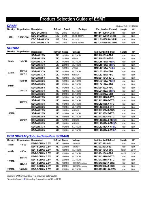
DRAMUpdated Date : 11/06/2006DensityOrganization DescriptionRefreshSpeedPackagePart Number(Pb-free)Sample MP EDO DRAM 5V 51225ns 40L-SOJ M11B416256A-25JP Now Now EDO DRAM 5V 51235ns 44-40L-TSOPII M11B416256A-35TG Now Now EDO DRAM 3.3V 51235ns 40L-SOJ M11L416256SA-35JP Now Now EDO DRAM 3.3V 51235ns 40/44L-TSOPIIM11L416256SA-35TGNowNowSDRAMDensityOrganization DescriptionRefresh SpeedPackagePart Number(Pb-free)Sample MP SDRAM 2.5V 2K 143MHz 50L-TSOPII M12S16161A-7TG Now Now SDRAM 2.5V 2K 143MHz VFBGA M12S16161A-7BG Now Now SDRAM 3.3V 2K 143MHz 50L-TSOPII M12L16161A-7T (I)G Now Now SDRAM 3.3V 2K 200MHz 50L-TSOPII M12L16161A-5T (I)G Now Now SDRAM 3.3V 2K 143MHz VFBGA M12L16161A-7B (I)G Now Now 2M*16SDRAM 3.3V 2K 143MHz 54L-TSOPII M12L32162A-7TG Now Now 1M*32SDRAM 3.3V 2K 143MHz 90-FBGA M12L32321A-7BG Now Now SDRAM 2.5V 4K 100MHz 54L-TSOPII M12S64164A-10TG Now Now SDRAM 3.3V 4K 143MHz 54L-TSOPII M12L64164A-7T (I)G Now Now SDRAM 3.3V 4K 200MHz 54L-TSOPII M12L64164A-5TG Now Now SDRAM 2.5V 4K 143MHz 86L-TSOPII M12S64322A-7TG Now Now SDRAM 3.3V 4K 166MHz 86L-TSOPII M12L64322A-6T (I)G Now Now SDRAM 3.3V 4K 200MHz 86L-TSOPII M12L64322A-5TG Now Now SDRAM 2.5V 4K 143MHz 54L-TSOPII M12S128168A-7TG Now Now SDRAM 2.5V 4K 166MHz 54L-TSOPII M12S128168A-6TG Now Now SDRAM 3.3V 4K 143MHz 54L-TSOPII M12L128168A-7TG Now Now SDRAM 3.3V 4K 166MHz 54L-TSOPII M12L128168A-6TG Now Now SDRAM 2.5V 4K 166MHz 90-FBGA M12S128324A-6BG Now Now SDRAM 2.5V 4K 143MHz 86L-TSOPII M12S128324A-7TG Now Now SDRAM 2.5V 4K 166MHz 86L-TSOPII M12S128324A-6TG Now Now SDRAM 3.3V 4K 143MHz 90-FBGA M12L128324A-7B (I)G Now Now SDRAM 3.3V 4K 166MHz 90-FBGA M12L128324A-6B (I)G Now Now SDRAM 3.3V 4K 143MHz 86L-TSOPII M12L128324A-7T (I)G Now Now SDRAM 3.3V4K166MHz86L-TSOPIIM12L128324A-6T (I)GNowNowDDR SDRAM (Dobule-Date-Rate SDRAM)Density Organization DescriptionRefresh SpeedPackagePart Number(Pb-free)Sample MP DDR-SDRAM 2.5V 4K 166MHz 100-LQFP M13S32321A-6L Now Now DDR-SDRAM 2.5V 4K 200MHz 100-LQFP M13S32321A-5L Now Now DDR-SDRAM 2.5V 4K 166MHz 66L-TSOPII M13S64164A-6TG Q2'07Q3'07DDR-SDRAM 2.5V 4K 200MHz 66L-TSOPII M13S64164A-5TG Q2'07Q3'07DDR-SDRAM 2.5V 4K 166MHz 66L-TSOPII M13S128168A-6TG Now Now DDR-SDRAM 2.5V 4K 200MHz 66L-TSOPII M13S128168A-5TG Now Now DDR-SDRAM 2.5V 4K 166MHz 144-FBGA (12x12mm)M13S128324A-6BG Now Now DDR-SDRAM 2.5V 4K 200MHz 144-FBGA (12x12mm)M13S128324A-5BG Now Now 256Mb16Mx16DDR-SDRAM 2.5V 4K200MHz66L-TSOPIIM13S2561616A-5TGNowNow*Identifier of Pb-free as G or P is shown on outer carton.**Industrial spec : (I) Operating temperature -40ºC ~+85 ºC.2M*3264Mb4Mb*1632Mb4Mb 256Kb*161Mb*1616Mb 128Mb8M*164Mx324M*32128Mb8M*1632Mb 64Mb1M*324M*16Mobile SDRAMDensityOrganizationDescriptionRefresh Speed Package & MCPPart Number(Pb-free)Sample MP Mobile SDRAM 2.5V4K 100MHz 50L-TSOPII M52S16161A-10T (I)G Now Now Mobile SDRAM 2.5V 4K 125MHz 50L-TSOPII M52S16161A-8T (I)G Now Now Mobile SDRAM 1.8V4K 100MHz50L-TSOPIIM52D16161A-10T (I)G Now Now Mobile SDRAM 2.5V 4K 100MHz 54L-TSOPII M52S32162A-10T (I)G Now Now Mobile SDRAM 2.5V 4K 100MHz 54-FBGA M52S32162A-10B (I)G Now Now Mobile SDRAM 2.5V 4K 133MHz 54L-TSOPII M52S32162A-7.5T (I)G Now Now Mobile SDRAM 2.5V 4K 133MHz 54-FBGA M52S32162A-7.5B (I)G Now Now Mobile SDRAM 1.8V 4K 100MHz 54L-TSOPII M52D32162A-10T (I)G Now Now Mobile SDRAM 1.8V 4K 100MHz 54-FBGA M52D32162A-10B (I)G Now Now Mobile SDRAM 1.8V 4K 100MHz 54L-TSOPII M52D32162A-7.5T (I)G Now Now Mobile SDRAM 1.8V 4K 133MHz 54-FBGA M52D32162A-7.5B (I)G Now Now Mobile SDRAM 2.5V 4K 100MHz 90-FBGA M52S32321A-10B (I)G Now Now Mobile SDRAM 2.5V 4K 133MHz 90-FBGA M52S32321A-7.5B (I)G Now Now Mobile SDRAM 1.8V 4K 100MHz 90-FBGA M52D32321A-10B (I)G Now Now Mobile SDRAM 1.8V 4K 133MHz 90-FBGA M52D32321A-7.5B (I)G Now Now Mobile SDRAM 2.5V 4K 100MHz 54L-TSOPII M52S64164A-10T (I)G Q2 '07Q3 '07Mobile SDRAM 2.5V 4K 100MHz 54-FBGA M52S64164A-10B (I)G Q2 '07Q3 '07Mobile SDRAM 2.5V 4K 133MHz 54L-TSOPII M52S64164A-7.5T (I)G Q2 '07Q3 '07Mobile SDRAM 2.5V 4K 133MHz 54-FBGA M52S64164A-7.5B (I)G Q2 '07Q3 '07Mobile SDRAM 1.8V 4K 100MHz 54L-TSOPII M52D64164A-10T (I)G Q2 '07Q3 '07Mobile SDRAM 1.8V 4K 100MHz 54-FBGA M52D64164A-10B (I)G Q2 '07Q3 '07Mobile SDRAM 1.8V 4K 100MHz 54L-TSOPII M52D64164A-7.5T (I)G Q2 '07Q3 '07Mobile SDRAM 1.8V 4K 133MHz 54-FBGA M52D64164A-7.5B (I)G Q2 '07Q3 '07Mobile SDRAM 2.5V 4K 100MHz 86L-TSOPII M52S64322A-10T (I)G Q2 '07Q3 '07Mobile SDRAM 2.5V 4K 100MHz 90-FBGA M52S64322A-10B (I)G Q2 '07Q3 '07Mobile SDRAM 2.5V 4K 133MHz 86L-TSOPII M52S64322A-7.5T (I)G Q2 '07Q3 '07Mobile SDRAM 2.5V 4K 133MHz 90-FBGA M52S64322A-7.5B (I)G Q2 '07Q3 '07Mobile SDRAM 1.8V 4K 100MHz 86L-TSOPII M52D64322A-10T (I)G Q2 '07Q3 '07Mobile SDRAM 1.8V 4K 100MHz 90-FBGA M52D64322A-10B (I)G Q2 '07Q3 '07Mobile SDRAM 1.8V 4K 100MHz 86L-TSOPII M52D64322A-7.5T (I)G Q2 '07Q3 '07Mobile SDRAM 1.8V4K133MHz 90-FBGAM52D64322A-7.5B (I)GQ2 '07Q3 '07*Identifier of Pb-free as G or P is shown on outer carton.**Industrial spec : (I) Operating temperature -40ºC ~+85 ºC.64Mb4Mx162Mx32(1)All Mobile functions are included : PASR,TCSR,DS,Deep power down mode.(2)Max. Icc6 : Self-refresh current with full bank in 70 ºC .1Mx16Max. Icc6= 75uA (1.8V)16Mb32Mb2Mx161Mx32。
K9F1208中文资料

NAND Flash芯片K9F1208资料一 NAND FlaSh和NOR Flash闪存(Flash Memory)由于其具有非易失性、电可擦除性、可重复编程以及高密度、低功耗等特点,被广泛地应用于手机、MP3、数码相机、笔记本电脑等数据存储设备中。
NAND Flash和NOR Flash是目前市场上两种主要的非易失闪存芯片。
与NOR Flash相比,NAND Flash 在容量、功耗、使用寿命等方面的优势使其成为高数据存储密度的理想解决方案。
NOR Flash的传输效率很高,但写入和擦除速度较低;而NAND Flash以容量大、写速度快、芯片面积小、单元密度高、擦除速度快、成本低等特点,在非易失性类存储设备中显现出强劲的市场竞争力。
结构:NOR Flash为并行,NAND Flash为串行。
总线:NOR Flash为分离的地址线和数据线,而NANDFlash为复用的。
尺寸:典型的NAND Flash尺寸为NOR Flash尺寸的1/8。
坏块:NAND器件中的坏块是随机分布的,需要对介质进行初始化扫描以发现坏块,并将坏块标记为不可用。
位交换:NAND Flash中发生的次数要比NOR Flash多,建议使用NAND闪存时,同时使用EDC/ECC算法。
使用方法:NOR Flash是可在芯片内执行(XIP,eXecute In Place),应用程序可以直接在FIash闪存内运行,不必再把代码读到系统RAM 中;而NAND Flash则需I/O接口,因此使用时需要写入驱动程序。
通过以上的分析和比较,NAND Flash更适合于大容量数据存储的嵌入式系统。
本设计选用Samsung公司生产的NAND Flash存储器芯片K9F1208作为存储介质,并应用在基于uPSD3234A增强型8051单片机的嵌入式系统中。
二K9F1208介绍K9F1208是Samsung公司生产的512 Mb(64M×8位)NAND Flash 存储器。
K9F2808U0资料

K9F2808U0A-YCB0, K9F2808U0A-YIB0
Document Title
16M x 8 Bit NAND Flash Memory
FLASH MEMORY
Revision History
Revision No. History
0.0 0.1 0.2 Initial issue. 1. Revised real-time map-out algorithm(refer to technical notes) 1. Changed device name - KM29U128AT -> K9F2808U0A-YCB0 - KM29U128AIT -> K9F2808U0A-YIB0 1. Changed sequential row read opera tion - The Sequential Read 1 and 2 operation is allowed only within a block 2. Changed invalid block(s) marking method prior to shipping - The invalid block(s) information is written the 1st or 2nd page of the invalid block(s) with 00h data --->The invalid block(s) status is defined by the 6th byte in the spare area. Samsung makes sure that either the 1st or 2nd page of every invalid block has 00h data at the column address of 517. 1. Changed endurance : 1million -> 100K program/erase cycles 2. Changed invalid block(s) marking method prior to shipping - The invalid block(s) status is defined by the 6th byte in the spare area. Samsung makes sure that either the 1st or 2nd page of every invalid block has 00h data at the column address of 517. --->The invalid block(s) status is defined by the 6th byte in the spare area. Samsung makes sure that either the 1st or 2nd page of every invalid block has non-FFh data at the column address of 517. 1. Changed SE pin description - SE is recommended to coupled to GND or Vcc and should not be toggled during reading or programming.
KF8TS2508 2510 2514 数据手册 V1.6 芯旺微电子说明书
KF8TS2508/2510/2514数据手册V1.68位微控制器KF8TS2508/10/14数据手册KF8TS2508/2510/2514数据手册V1.6芯旺微电子 - 2/156 -产品订购信息芯片型号订货号封装FLASHRAM(Byte)内部HFOSC(Hz)外部HF/LFOSC(Hz)8位定时器16位定时器8位PWM12位ADC触摸按键I2C内部参考电压工作电压(V)KF8TS2508 KF8TS2508SD SOIC-14 4Kx16 40016M16M/ 32.768k13288 1 2V/3V/4V 2.6~5.5 KF8TS2510KF8TS2510SE SOIC-16 1010KF8TS2514KF8TS2514SG SOIC-20 1414KF8TS2514OG SSOP-20 KF8TS2514NG QFN-20版权所有@上海芯旺微电子有限公司 本文档为上海芯旺微电子有限公司在现有数据资料基础上慎重且力求准确无误编制而成.确保应用符合技术规范,是您自身应负的责任。
上海芯旺微电子有限公司不作任何明示或暗示、书面或口头、法定或其他形式的声明或担保,包括但不限于针对其使用情况、质量、性能、适销性或特定用途的适用性的声明或担保。
上海芯旺微电子有限公司对因这些信息及使用这些信息而引起的后果不承担任何责任。
如果将芯旺微电子有限公司的芯片用于生命维持和或生命安全应用,一切风险由使用方自负。
使用方同意在由此引发任何一切伤害、索赔、诉讼或费用时,会维护和保障上海芯旺微电子有限公司免于承担法律责任,并加以赔偿。
本文档中所述的器件应用信息及其他类似内容仅为您提供便利,可能有更新的信息所替代。
上海芯旺微电子有限公司会不定期进行更新,恕不另行通知。
使用方如需获得最新的产品信息,请及时访问上海芯旺微电子有限公司官网或与上海芯旺微电子有限公司联系。
KF8TS25XX芯片使用注意事项芯片的ESD防护措施KF8TS25XX芯片提供满足工业级ESD标准保护电路。
K9K1G08U0B资料

Document Title128M x 8 Bit NAND Flash Memory Revision HistoryThe attached data sheets are prepared and approved by SAMSUNG Electronics. SAMSUNG Electronics CO., LTD. reserve the rightto change the specifications. SAMSUNG Electronics will evaluate and reply to your requests and questions about device. If you have any questions, please contact the SAMSUNG branch office near your office.Revision No.0.00.1RemarkAdvance AdvanceHistoryInitial issue.1. Note 1 ( Program/Erase Characteristics) is added( page 13 )2. NAND Flash Technical Notes is changed.-Invalid block -> initial invalid block ( page 15 ) -Error in write or read operation ( page 16 ) -Program Flow Chart ( page 16 )3. Vcc range is changed-1.7V~1.95V ->1.65V~1.95V 4. 2.7V device is added5. Multi plane operation and Copy-Back Program are not supported with 1.8Vdevice.Draft DateMar. 17th 2003Oct. 11th 2004Note : For more detailed features and specifications including FAQ, please refer to Samsung’s Flash web site. /Products/Semiconductor/Flash/TechnicalInfo/datasheets.htm128M x 8 Bit Bit NAND Flash MemoryThe K9K1G08X0B is a 128M(134,217,728)x8bit NAND Flash Memory with a spare 4.096K(4,194,304)x8bit. Its NAND cell provides the most cost-effective solution for the solid state mass storage market. A program operation can be performed in typically 200µs on the 528-byte page and an erase operation can be performed in typically 2ms on a 16K-byte block. Data in the data register can be read out at 50ns(1.8V device : 60ns) cycle time per byte. The I/O pins serve as the ports for address and data input/output as well as command inputs. The on-chip write controller automates all program and erase functions including pulse repetition, where required,and internal verify and margining of data. Even the write-intensive systems can take advantage of the K9K1G08X0B ′s extended reli-ability of 100K program/erase cycles by providing ECC(Error Correcting Code) with real time mapping-out algorithm. The K9K1G08X0B is an optimum solution for large nonvolatile storage applications such as solid state file storage and other portable applications requiring non-volatility.GENERAL DESCRIPTIONFEATURESPRODUCT LISTPart Number Vcc Range OrganizationPKG TypeK9K1G08R0B-G,J 1.65 ~ 1.95V X8FBGAK9K1G08B0B-G,J 2.5 ~ 2.9V K9K1G08U0B-G,J2.7 ~3.6V• Voltage Supply- 1.8V device(K9K1G08R0B) : 1.65 ~ 1.95V - 2.7V device(K9K1G08B0B) : 2.5 ~ 2.9V - 3.3V device(K9K1GXXU0B) : 2.7 ~ 3.6 V • Organization- Memory Cell Array-128M + 4096K)bit x 8 bit - Data Register- (512 + 16)bit x 8bit• Automatic Program and Erase - Page Program - (512 + 16)Byte - Block Erase : - (16K + 512)Byte• Page Read Operation - Page Size- (512 + 16)Byte- Random Access : 15µs(Max.) - Serial Page Access : 50ns(Min.)* * K9K1G08R0B : 60ns • Fast Write Cycle Time- Program time : 200µs(Typ.) - Block Erase Time : 2ms(Typ.)• Command/Address/Data Multiplexed I/O Port • Hardware Data Protection- Program/Erase Lockout During Power Transitions • Reliable CMOS Floating-Gate Technology- Endurance : 100K Program/Erase Cycles - Data Retention : 10 Years • Command Register Operation • Intelligent Copy-Back• Unique ID for Copyright Protection • Package- K9K1G08X0B-GCB0/GIB0 63- Ball FBGA- K9K1G08X0B-JCB0/JIB063- Ball FBGA - Pb-free PackageK9K1G08X0B-GCB0,JCB0/GIB0,JIB0PIN CONFIGURATION (FBGA)R/B /WE /CE Vss ALE /WP /RE CLE NC NC NCNCVcc NC NC I/O0I/O1NC NCVccQ I/O5I/O7VssI/O6I/O4I/O3I/O2VssNC NC NC NC NC NC NC NC NC NC NC NC NC NC NC NC NC NC NC NC N.CN.C N.C N.C N.C N.CN.CN.CN.C N.C N.C N.CN.C N.C N.C34561 2A B CD GEF HTop View8.50±0.10#A1Side ViewTop View 1.20(M a x )0.45±0.054321A BC D G Bottom View13.50±0.1063-∅0.45±0.050.80 x 7= 5.6013.50±0.100.80 x 5= 4.00 0.800.25(M i n .)0.10MAXBA2.802.008.50±0.10(Datum B)(Datum A)0.20 M A B∅0.800.80 x 11= 8.800.80 x 9= 7.20 6513.50±0.10EF H#A1 INDEX MARK(OPTIONAL)PIN DESCRIPTIONNOTE : Connect all V CC and V SS pins of each device to common power supply outputs.Do not leave V CC or V SS disconnected.Pin Name Pin FunctionI/O 0 ~ I/O 7(K9K1G08X0B)DATA INPUTS/OUTPUTSThe I/O pins are used to input command, address and data, and to output data during read operations. The I/O pins float to high-z when the chip is deselected or when the outputs are disabled.CLECOMMAND LATCH ENABLEThe CLE input controls the activating path for commands sent to the command register. When active high, commands are latched into the command register through the I/O ports on the rising edge of the WE signal.ALEADDRESS LATCH ENABLEThe ALE input controls the activating path for address to the internal address registers. Addresses are latched on the rising edge of WE with ALE high.CECHIP ENABLEThe CE input is the device selection control. When the device is in the Busy state, CE high is ignored, and the device does not return to standby mode in program or erase operation. Regarding CE control during read operation, refer to ’Page read’ section of Device operation .REREAD ENABLEThe RE input is the serial data-out control, and when active drives the data onto the I/O bus. Data is valid tREA after the falling edge of RE which also increments the internal column address counter by one.WEWRITE ENABLEThe WE input controls writes to the I/O port. Commands, address and data are latched on the rising edge of the WE pulse.WPWRITE PROTECTThe WP pin provides inadvertent write/erase protection during power transitions. The internal high voltage generator is reset when the WP pin is active low.R/BREADY/BUSY OUTPUTThe R/B output indicates the status of the device operation. When low, it indicates that a program, erase or random read operation is in process and returns to high state upon completion. It is an open drain output and does not float to high-z condition when the chip is deselected or when outputs are disabled.Vcc QOUTPUT BUFFER POWERVcc Q is the power supply for Output Buffer.Vcc Q is internally connected to Vcc, thus should be biased to Vcc.Vcc POWERV CC is the power supply for device. Vss GROUNDN.C NO CONNECTIONLead is not internally connected.DNUDO NOT USELeave it disconnected.Product IntroductionThe K9K1G08X0B is a 1,026Mbit(1,107,296,436 bit) memory organized as 262,144 rows(pages) by 528 columns. Spare sixteen col-umns are located from column address of 512 to 527. A 528-byte data register is connected to memory cell arrays accommodating data transfer between the I/O buffers and memory during page read and page program operations. The memory array is made up of 16 cells that are serially connected to form a NAND structure. Each of the 16 cells resides in a different page. A block consists of two NAND structured strings. A NAND structure consists of 16 cells. Total 135168 NAND cells reside in a block. The array organization is shown in Figure 2. The program and read operations are executed on a page basis, while the erase operation is executed on a block basis. The memory array consists of 8,192 separately erasable 16K-byte blocks. It indicates that the bit by bit erase operation is pro-hibited on the K9K1G08X0B.The K9K1G08X0B has addresses multiplexed into 8 I/O's. This scheme dramatically reduces pin counts and allows systems upgrades to future densities by maintaining consistency in system board design. Command, address and data are all written through I/O's by bringing WE to low while CE is low. Data is latched on the rising edge of WE. Command Latch Enable(CLE) and Address Latch Enable(ALE) are used to multiplex command and address respectively, via the I/O pins. The 128M byte physical space requires 27 addresses, thereby requiring four cycles for byte-level addressing: column address, low row address and high row address, in that order. Page Read and Page Program need the same four address cycles following the required command input. In Block Erase oper-ation, however, only the three row address cycles are used. Device operations are selected by writing specific commands into the command register. Table 1 defines the specific commands of the K9K1G08X0B.The device provides simultaneous program/erase capability up to four pages/blocks. By dividing the memory array into eight 128Mbit separate planes, simultaneous multi-plane operation dramatically increases program/erase performance by 4X while still maintaining the conventional 512 byte structure.The extended pass/fail status for multi-plane program/erase allows system software to quickly identify the failing page/block out of selected multiple pages/blocks. Usage of multi-plane operations will be described further throughout this document.In addition to the enhanced architecture and interface, the device incorporates copy-back program feature from one page to another of the same plane without the need for transporting the data to and from the external buffer memory. Since the time-consuming burst-reading and data-input cycles are removed, system performance for solid-state disk application is significantly increased.Table 1. Command SetsFunction1st. Cycle2nd. Cycle3rd. Cycle Acceptable Command during Busy Read 100h/01h(1)--Read 250h--Read ID90h--Reset FFh--OPage Program (True)(2)80h10h-Page Program (Dummy)(2)80h11h-Copy-Back Program(True)(2)00h8Ah10hCopy-Back Program(Dummy)(2)03h8Ah11hBlock Erase60h D0h-Multi-Plane Block Erase60h---60h D0h-Read Status70h--ORead Multi-Plane Status71h(3)--ONOTE : 1. The 00h command defines starting address of the 1st half of registers.The 01h command defines starting address of the 2nd half of registers.After data access on the 2nd half of register by the 01h command, the status pointer isautomatically moved to the 1st half register(00h) on the next cycle.2. Page Program(True) and Copy-Back Program(True) are available on 1 plane operation.Page Program(Dummy) and Copy-Back Program(Dummy) are available on the 2nd,3rd,4th plane of multi plane operation.3. The 71h command should be used for read status of Multi Plane operation.4. Multi plane operation and Copy-Back Program are not supported with 1.8V device.Caution : Any undefined command inputs are prohibited except for above command set of Table 1.RECOMMENDED OPERATING CONDITIONS(Voltage reference to GND, K9K1G08X0B-XCB0 :T A =0 to 70°C, K9K1G08X0B-XIB0 :T A =-40 to 85°C)Parameter Symbol K9K1G08R0B(1.8V)K9K1G08B0B(2.7V)K9K1G08U0B(3.3V)Unit Min Typ.Max Min Typ.Max Min Typ.Max Supply Voltage V CC 1.65 1.8 1.95 2.5 2.7 2.9 2.7 3.3 3.6V Supply Voltage V CCQ 1.65 1.8 1.95 2.5 2.7 2.9 2.7 3.3 3.6V Supply VoltageV SSVABSOLUTE MAXIMUM RATINGSNOTE :1. Minimum DC voltage is -0.6V on input/output pins. During transitions, this level may undershoot to -2.0V for periods <30ns.Maximum DC voltage on input/output pins is V CC,+0.3V which, during transitions, may overshoot to V CC +2.0V for periods <20ns.2. Permanent device damage may occur if ABSOLUTE MAXIMUM RATINGS are exceeded. Functional operation should be restricted to the conditions as detailed in the operational sections of this data sheet. Exposure to absolute maximum rating conditions for extended periods may affect reliability.ParameterSymbol RatingUnit1.8V Device2.7V/3.3V Device Voltage on any pin relative to V SSV IN/OUT-0.6 to + 2.45-0.6 to + 4.6V V CC -0.2 to + 2.45-0.6 to + 4.6V CCQ-0.2 to + 2.45-0.6 to + 4.6Temperature Under Bias K9K1G08X0B-XCB0T BIAS -10 to +125°C K9K1G08X0B-XIB0-40 to +125Storage Temperature K9K1G08X0B-XCB0T STG -65 to +150°C K9K1G08X0B-XIB0Short Circuit CurrentIos5mADC AND OPERATING CHARACTERISTICS (Recommended operating conditions otherwise noted.)NOTE : V IL can undershoot to -0.4V and V IH can overshoot to V CC +0.4V for durations of 20 ns or lessParameterSymbolTest ConditionsK9K1G08X0BUnit1.8V2.7V3.3V MinTyp Max Min Typ Max Min Typ Max Operating CurrentSequentialRead I CC 1tRC=50ns(K9K1G08R0B:60ns), CE=V IL I OUT =0mA-1020-1020-1530mAProgramI CC 2--1020-1020-1530EraseI CC 3--1020-1020-1530Stand-by Current (TTL)I SB 1CE=V IH , WP=0V/V CC --1--1--1Stand-by Current (CMOS)I SB 2CE=V CC -0.2, WP=0V/V CC -20100-1050-20100µAInput Leakage Current I LI V IN =0 to Vcc(max)--±20--±10--±20Output Leakage CurrentI LOV OUT =0 to Vcc(max)--±20--±10--±20Input High VoltageV IH*I/O pinsV CCQ -0.4-V CCQ +0.3V CCQ-0.4-V CCQ +0.3 2.0-V CCQ +0.3VExcept I/O pinsV CC -0.4-V CC +0.3V CC -0.4-V CC +0.3 2.0-V CC +0.3Input Low Voltage, All inputsV IL*--0.3-0.4-0.3-0.5-0.3-0.8Output High Voltage LevelV OHK9K1G08R0B :I OH -100µAK9K1G08B0B :I OH -100µA K9K1G08U0B :I OH -400µA V CCQ-0.1--V CCQ -0.4-- 2.4--Output Low Voltage LevelV OLK9K1G08R0B :I OL =100uAK9K1G08B0B :I OH =100µA K9K1G08U0B :I OL =2.1mA --0.1--0.4--0.4Output Low Current (R/B)I OL (R/B)K9K1G08R0B :V OL =0.1VK9K1G08B0B :V OL =0.1VK9K1G08U0B :V OL =0.4V34-34-810-mAValid BlockNOTE :1. The device may include invalid blocks when first shipped. Additional invalid blocks may develop while being used. The number of valid blocks is pre-sented with both cases of invalid blocks considered. Invalid blocks are defined as blocks that contain one or more bad bits. Do not try to access these invalid blocks for program and erase. Refer to the attached technical notes for an appropriate management of invalid blocks.2. The 1st block, which is placed on 00h block address, is guaranteed to be a valid block, does not require Error Correction up to 1K program/erase cycles.3. Minimum 1004 valid blocks are guaranteed for each contiguous 128Mb memory space.ParameterSymbol Min Typ.Max Unit Valid Block NumberN VB8,052-8,192BlocksProgram / Erase CharacteristicsParameterSymbol Min Typ Max Unit Program Time t PROG (1)-200500µs Dummy Busy Time for Multi Plane Program t DBSY 110µs Number of Partial Program Cycles in the Same Page Main Array Nop --1cycle Spare Array--2cycles Block Erase Timet BERS-23msCapacitance (T A =25°C, V CC =1.8V/2.7V/3.3V, f=1.0MHz)NOTE : Capacitance is periodically sampled and not 100% tested.ItemSymbol Test ConditionMin Max Unit Input/Output Capacitance C I/O V IL =0V -20pF Input CapacitanceC INV IN =0V-20pFAC TEST CONDITION(K9K1G08X0B-XCB0 :TA=0 to 70°C, K9K1G08X0B-XIB0 :TA=-40 to 85°CK9K1G08R0B : Vcc=1.65V~1.95V , K9K1G08B0B : Vcc=2.5V~2.9V, K9K1G08U0B : Vcc=2.7V~3.6V unless otherwise noted)ParameterK9K1G08R0B K9K1G08B0B K9K1G08U0B Input Pulse Levels 0V to Vcc Q0V to Vcc Q0.4V to 2.4VInput Rise and Fall Times 5ns 5ns 5ns Input and Output Timing LevelsVcc Q /2Vcc Q /21.5VK9K1G08R0B:Output Load (Vcc Q :1.8V +/-10%)K9K1G08B0C:Output Load (Vcc Q :2.7V +/-10%)K9K1G08U0B:Output Load (Vcc Q :3.0V +/-10%) 1 TTL GATE and CL=30pF 1 TTL GATE and CL=30pF 1 TTL GATE and CL=50pF K9K1G08U0B:Output Load (Vcc Q :3.3V +/-10%)-- 1 TTL GATE and CL=100pFMODE SELECTIONNOTE : 1. X can be V IL or V IH.2. WP should be biased to CMOS high or CMOS low for standby.CLE ALE CE WERE WP ModeH L L H X Read Mode Command Input L H L H X Address Input(4clock)H L L H H Write Mode Command Input L H L H H Address Input(4clock)L L L HH Data Input L L L H X Data OutputX X X X H X During Read(Busy) on the devices X X X X X H During Program(Busy)X X X X X H During Erase(Busy)X X (1)X X X LWrite ProtectXXHXX0V/V CC (2) Stand-byNOTE : 1.Typical program time is defined as the time within which more than 50% of the whole pages are programmed at Vcc of 3.3V and 25’CAC Characteristics for OperationNOTE : 1. If reset command(FFh) is written at Ready state, the device goes into Busy for maximum 5us.ParameterSymbol MinMax Unit 1.8V 2.7V 3.3V 1.8V 2.7V 3.3V Data Transfer from Cell to Register t R 0--151515µs ALE to RE Delay t AR 101010---ns CLE to RE Delay t CLR 101010---ns Ready to RE Low t RR 202020---ns RE Pulse Width t RP 402525---ns WE High to Busy t WB ---100100100ns Read Cycle Time t RC 605050---ns RE Access Time t REA ---403030ns CE Access Time t CEA ---554545ns RE High to Output Hi-Z t RHZ ---303030ns CE High to Output Hi-Z t CHZ ---202020ns RE or CE High to Output hold t OH 151515---ns RE High Hold Time t REH 201515---ns Output Hi-Z to RE Low t IR 000---ns WE High to RE Lowt WHR 606060---ns Device Resetting Time(Read/Program/Erase)t RST---5/10/500(1)5/10/500(1)5/10/500(1)µsAC Timing Characteristics for Command / Address / Data InputNOTE : 1. If tCS is set less than 10ns, tWP must be minimum 35ns, otherwise, tWP may be minimum 25ns.Parameter Symbol MinMax Unit 1.8V 2.7V 3.3V 1.8V 2.7V 3.3V CLE Set-up Time t CLS 000---ns CLE Hold Time t CLH 101010---ns CE Setup Time t CS 000.-.-.-ns CE Hold Time t CH 101010---ns WE Pulse Width t WP 4025(1)25(1)---ns ALE Setup Time t ALS 000---ns ALE Hold Time t ALH 101010---ns Data Setup Time t DS 202020---ns Data Hold Time t DH 101010---ns Write Cycle Time t WC 605050---ns WE High Hold Timet WH201515---ns*Check "FFh" at the column address 517 Figure 4. Flow chart to create initial invalid block table.StartSet Block Address = 0Check "FFh" ?Increment Block AddressLast Block ?EndNoYesYesCreate (or update)No Initial Invalid Block(s) Tableof the 1st and 2nd page in the blockNAND Flash Technical NotesIdentifying Initial Invalid Block(s)Initial Invalid Block(s)Initial invalid blocks are defined as blocks that contain one or more initial invalid bits whose reliability is not guaranteed by Samsung.The information regarding the initial invalid block(s) is so called as the initial invalid block information. Devices with initial invalid block(s) have the same quality level as devices with all valid blocks and have the same AC and DC characteristics. An initial invalid block(s) does not affect the performance of valid block(s) because it is isolated from the bit line and the common source line by a select transistor. The system design must be able to mask out the initial invalid block(s) via address mapping. The 1st block, which is placed on 00h block address, is guaranteed to be a valid block, does not require Error Correction up to 1K program/erase cycles.All device locations are erased(FFh) except locations where the initial invalid block(s) information is written prior to shipping. The initial invalid block(s) status is defined by the 6th byte in the spare area. Samsung makes sure that either the 1st or 2nd page of every initial invalid block has non-FFh data at the column address of 517. Since the initial invalid block information is also erasable in most cases, it is impossible to recover the information once it has been erased. Therefore, the system must be able to recognize the initial invalid block(s) based on the initial invalid block information and create the initial invalid block table via the following sug-gested flow chart(Figure 4). Any intentional erasure of the initial invalid block information is prohibited.NAND Flash Technical Notes (Continued)Program Flow ChartStartI/O 6 = 1 ?I/O 0 = 0 ?No*Write 80hWrite AddressWrite DataWrite 10hRead Status RegisterProgram Completedor R/B = 1 ?Program ErrorYesNoYesError in write or read operationWithin its life time, additional invalid blocks may develop with NAND Flash memory. Refer to the qualification report for the block failure rate.The following possible failure modes should be considered to implement a highly reliable system. In the case of status read failure after erase or program, block replacement should be done. Because program status fail during a page program does not affect the data of the other pages in the same block, block replacement can be executed with a page-sized buffer by finding an erased empty block and reprogramming the current target data and copying the rest of the replaced block. In case of Read, ECC must be employed. To improve the efficiency of memory space, it is recommended that the read failure due to single bit error should be reclaimed by ECC without any block replacement. The block failure ratein the qualification report does not include those reclaimed blocks.Failure ModeDetection and Countermeasure sequenceWrite Erase Failure Status Read after Erase --> Block Replacement Program Failure Status Read after Program --> Block Replacement ReadSingle Bit FailureVerify ECC -> ECC CorrectionECC: Error Correcting Code --> Hamming Code etc. Example) 1bit correction & 2bit detection: If program operation results in an error, map out the block including the page in error and copy the*target data to another block.Erase Flow ChartStart I/O 6 = 1 ?I/O 0 = 0 ?No*Write 60h Write Block AddressWrite D0h Read Status Registeror R/B = 1 ?Erase ErrorYesNo: If erase operation results in an error, map out the failing block and replace it with another block.* Erase CompletedYesRead Flow ChartStart Verify ECCNoWrite 00h Write Address Read Data ECC GenerationReclaim the ErrorPage Read CompletedYesBlock ReplacementNAND Flash Technical Notes (Continued)When the error happens with page "a" of Block "A", try to write the data into another Block "B" from an exter-nal buffer. Then, prevent further system access to Block "A" (by creating a "invalid block" table or other appropriate scheme.)Buffer memoryerror occursBlock ABlock BPage aSamsung NAND Flash has three address pointer commands as a substitute for the two most significant column addresses. ’00h’command sets the pointer to ’A’ area(0~255byte), ’01h’ command sets the pointer to ’B’ area(256~511byte), and ’50h’ command sets the pointer to ’C’ area(512~527byte). With these commands, the starting column address can be set to any of a whole page(0~527byte). ’00h’ or ’50h’ is sustained until another address pointer command is inputted. ’01h’ command, however, is effective only for one operation. After any operation of Read, Program, Erase, Reset, Power_Up is executed once with ’01h’ command, the address pointer returns to ’A’ area by itself. To program data starting from ’A’ or ’C’ area, ’00h’ or ’50h’ command must be inputted before ’80h’ command is written. A complete read operation prior to ’80h’ command is not necessary. To program data starting from ’B’ area, ’01h’ command must be inputted right before ’80h’ command is written.00h(1) Command input sequence for programming ’A’ areaAddress / Data input80h10h00h80h10hAddress / Data inputThe address pointer is set to ’A’ area(0~255), and sustained01h(2) Command input sequence for programming ’B’ areaAddress / Data input80h10h01h80h10hAddress / Data input’B’, ’C’ area can be programmed.It depends on how many data are inputted.’01h’ command must be rewritten before every program operationThe address pointer is set to ’B’ area(256~511), and will be reset to ’A’ area after every program operation is executed.50h(3) Command input sequence for programming ’C’ areaAddress / Data input80h10h50h80h10hAddress / Data inputOnly ’C’ area can be programmed.’50h’ command can be omitted.The address pointer is set to ’C’ area(512~527), and sustained’00h’ command can be omitted.It depends on how many data are inputted.’A’,’B’,’C’ area can be programmed.Pointer Operation of K9K1G08X0BTable 2. Destination of the pointerCommandPointer position Area 00h 01h 50h0 ~ 255 byte 256 ~ 511 byte 512 ~ 527 byte1st half array(A)2nd half array(B)spare array(C)"A" area 256 Byte(00h plane)"B" area (01h plane)"C" area (50h plane)256 Byte16 Byte"A""B""C"Internal Page RegisterPointer select commnad(00h, 01h, 50h)PointerFigure 5. Block Diagram of Pointer OperationRead ID OperationCECLEI/O 0 ~ 7WEALERE90hRead ID CommandMaker Code00h ECh t READAddress. 1cycleA5hC0h Multi Plane CodeID Defintition Table90 ID : Access command = 90HValueDescription1st Byte 2nd Byte 3rd Byte 4th ByteECh 79h A5h C0hMaker Code Device CodeMust be don’t -caredSupports Multi Plane Operation(Must be don’t-cared for 1.8V device)Device Device CodeK9K1G08R0B 78h K9K1G08B0B 79h K9K1G08U0B79hDevice* CodeDevice OperationPAGE READUpon initial device power up, the device defaults to Read1 mode. This operation is also initiated by writing 00h to the command reg-ister along with four address cycles. Once the command is latched, it does not need to be written for the following page read opera-tion. Three types of operations are available : random read, serial page read and sequential row read.The random read mode is enabled when the page address is changed. The 528 bytes of data within the selected page are trans-ferred to the data registers in less than 15µs(t R). The system controller can detect the completion of this data transfer(tR) by analyz-ing the output of R/B pin. Once the data in a page is loaded into the registers, they may be read out in 50ns(1.8V device : 60ns) cycle time by sequentially pulsing RE. High to low transitions of the RE clock output the data stating from the selected column address up to the last column address.The way the Read1 and Read2 commands work is like a pointer set to either the main area or the spare area. The spare area of bytes 512 to 527 may be selectively accessed by writing the Read2 command. Addresses A0 to A3 set the starting address of the spare area while addresses A4 to A7 are ignored. Unless the operation is aborted, the page address is automatically incremented for sequential row read as in Read1 operation and spare sixteen bytes of each page may be sequentially read. The Read1 com-mand(00h/01h) is needed to move the pointer back to the main area. Figures 9 to 12 show typical sequence and timings for each read operation.PAGE PROGRAMThe device is programmed basically on a page basis, but it does allow multiple partial page programing of a byte or consecutive bytes up to 528, in a single page program cycle. The number of consecutive partial page programming operation within the same page with-out an intervening erase operation must not exceed 1 for main array and 2 for spare array. The addressing may be done in any ran-dom order in a block. A page program cycle consists of a serial data loading period in which up to 528 bytes of data may be loaded into the page register, followed by a non-volatile programming period where the loaded data is programmed into the appropriate cell.Serial data loading can be started from 2nd half array by moving pointer. About the pointer operation, please refer to the attached technical notes.The serial data loading period begins by inputting the Serial Data Input command(80h), followed by the four cycle address input and then serial data loading. The bytes other than those to be programmed do not need to be loaded.The Page Program confirm com-mand(10h) initiates the programming process. Writing 10h alone without previously entering the serial data will not initiate the pro-gramming process. The internal write state control automatically executes the algorithms and timings necessary for program and verify, thereby freeing the system controller for other tasks. Once the program process starts, the Read Status Register command may be entered, with RE and CE low, to read the status register. The system controller can detect the completion of a program cycle by monitoring the R/B output, or the Status bit(I/O 6) of the Status Register. Only the Read Status command and Reset command are valid while programming is in progress. When the Page Program is complete, the Write Status Bit(I/O 0) may be checked(Figure 10).The internal write verify detects only errors for "1"s that are not successfully programmed to "0"s. The command register remains in Read Status command mode until another valid command is written to the command register.Figure 10. Program & Read Status Operation80hA 0 ~ A 7 & A 9 ~ A 26I/O 0~7R/B Address & Data Input I/O 0Pass528 Byte Data10h 70h Failt PROGFigure 11. Block Erase OperationBLOCK ERASEThe Erase operation is done on a block(16K Byte) basis. Block address loading is accomplished in three cycles initiated by an Erase Setup command(60h). Only address A 14 to A 26 is valid while A 9 to A 13 is ignored. The Erase Confirm command(D0h) following the block address loading initiates the internal erasing process. This two-step sequence of setup followed by execution command ensures that memory contents are not accidentally erased due to external noise conditions.At the rising edge of WE after the erase confirm command input, the internal write controller handles erase and erase-verify. When the erase operation is completed, the Write Status Bit(I/O 0) may be checked. Figure 11 details the sequence.60hBlock Add. : A 14 ~ A 26I/O 0~7R/B Address Input(3Cycle)I/O 0PassD0h70h Failt BERS。
K9F4G08U0E_1.2

1.1 1.2
Final Final
S.M.Lee S.M.Lee
H.H.Shin H.H.Shin
The attached data sheets are prepared and approved by SAMSUNG Electronics. SAMSUNG Electronics CO., LTD. reserve the right to change the specifications. SAMSUNG Electronics will evaluate and reply to your requests and questions about device. If you have any questions, please contact the SAMSUNG branch office near your office.
-1-
K9F4G08U0E K9K8G08U1E K9K8G08U0E K9WAG08U1E
datasheet
History Draft Date Oct. 30, 2012
SAMSUNG CONFIDENTIAL Rev. 1.2ision History
Revision No. 0.0 1.0 1. Initial issue Remark Target Final Edited by Reviewed by H.K.Kim H.K.Kim H.H.Shin H.H.Shin
-2-
K9F4G08U0E K9K8G08U1E K9K8G08U0E K9WAG08U1E
datasheet
SAMSUNG CONFIDENTIAL Rev. 1.2
FLASH MEMORY
Table Of Contents
- 1、下载文档前请自行甄别文档内容的完整性,平台不提供额外的编辑、内容补充、找答案等附加服务。
- 2、"仅部分预览"的文档,不可在线预览部分如存在完整性等问题,可反馈申请退款(可完整预览的文档不适用该条件!)。
- 3、如文档侵犯您的权益,请联系客服反馈,我们会尽快为您处理(人工客服工作时间:9:00-18:30)。
m A 5 5 15 15 1 10 10 20 20 1 µA 10 50 10 50
页 编 ICC2 程 擦除 ICC3 ISB1 等待状态电流 (TTL) 等待状态电流 (CMOS) 输入开漏电流 输出开漏电流
ISB2
IL1 IL0
-
-
±10 ±10
-
-
±10 ±10 VCC V +0.3 0.8 -
6. 命令/地址/ 数据复用端口: 7. 硬件数据保护:编程/擦除操作在电源转换时关闭。 8. 可靠的 CMOS 浮置门技术: --保证:100K 编程/ 擦除次数。 --数据保持时间: 10 年。 9. 命令寄存器操作 10. 为高速编程设置的缓冲编程操作。 11. 通电自动读操作。 12. 智能复制拷贝操作。 13.为防盗版而设置的唯一的 ID 保护。 14. 封装。 - K9F1GXXX0M-YCB0/YIB0 48 - Pin TSOP I (12 x 20 / 0.5 mm pitch) - K9F1G08U0M-VCB0/VIB0 48 - Pin WSOP I (12X17X0.7mm)
器件描述
三星 K9F1GXXX0M 提供了 128M*8Bit/64M*16Bit 的存储容量,另外还有 32 M 的空闲存储器,它是采用 NAND 技术的大容量、高可靠的 Flash 存储器。 它对 2112 字节一页(*8device )或者 1056 字(*16device)一页的写操作。典型 时间是 300 微秒。对 128 字节/64K 字一块的擦除时间是 50 纳秒。输出引脚可 以作为数据/地址/命令复用。每一页的数据读出时间也很快,平均每个字节只 需 50 纳秒。片内的写控制器,可以自动执行写操作和擦除功能,包括必要的脉 冲产生器,内部校验和冗余数据。 K9F1G08 提供了实时映像算法的纠错码,写 操作系统可以利用 K9F1G08U0M 扩展的 100K 编程/ 擦除。K9F1G08U0M 为大 容量存储,新型电可擦写的非易失性半导体存储器,提供了最优方案。
参数 供电电压 供电电压 特征位 VCC VSS K9F1GXXQOM(1.8V) Min Typ Max 1.65 1.8 1.95 0 0 0 K9F1GXXUOM(3.3V) Min Typ Max 2.7 3.3 3.6 0 0 0 Unit V V
电源和操作参数
参数 操 作 连续 电流 读页 特征 ICC1 测试条件 tRC=50ns, CE=VIL IOUT=0mA CE=VIH, WP=PRE=0V/V CC CE=VCC-0.2, WP=PRE=0V/V CC VIN=0 to Vcc(max) VOUT=0 to Vcc(max) K9F1GXXQ0M : IOH=-100µA K9F1GXXU0M : IOH=-400µA K9F1GXXQ0M : IOL=100uA K9F1GXXU0M : IOL=2.1mA K9F1GXXQ0M : VOL=0.1V K9F1GXXU0M : VOL=0.4V K9F1GXXQOM(1. 8V) Min Typ Max 5 15 K9F1GXXUOM(3. 3V) Min Typ Max 10 20 单 位
11. VSS:芯片接地端。 12. NC:悬空。 注意:把各个器件的VCC或者VSS 接到共同的电源输出端,不可以把VCC或者 VSS悬空。( 共地问题) 表1-1 K9F1G08*OM(*8) 功能化模块结构图
表2-1 K9F1G08*OM(*8) 存储阵列结构
注意: 列地址:寄存器开始的地址。 *L 必须被置低。 *除了要求的地址周期,存储器禁止输入任何额外的地址周期。 表 1-2 K9F1G16*OM(*16) 功能化模块结构图
K9F1G08UOM 数据手册
128M*8Bit/64M*16Bit NAND Flash Memory 产品列表 型号 K9F1G08QOM-Y K9F1G16QOM-Y K9F1G08UOM-Y K9F1G16UOM-Y K9F1G08UOM-V 供电电压范围 1.65~1.95V 2.7~3.6V 组织 X8 X8 X8 X8 X8 封装 TSOP1
任意引脚对地电压
Temperatu K9F1GXXXOM-YCBO/VC re Under BO Bias K9F1GXXXOM-YIBO/VIB O K9F1GXXXOM-YCBO/VC 存储温度 BO K9F1GXXXOM-YIBO/VIB O 短路电流
-40~+125
°C
IOS
5
mA
推荐操作条件
元阵列时,可以将数据写入缓冲寄存器。当在需要时将很多页数据写入的时候, 由于使用了缓冲写操作技术使得写入操作有很大的提高。 芯片包含了通电读操作。 可以在通电后第一页自动存取数据而不需要地 址和命令,除了增加结构和接口之外,器件提供了从一页到另一页的写操作技术 而不需要把数据传送到另外的缓冲存储区。
引脚名称(TSOP1)
封装尺寸
引脚名称(WSOP1)
封装尺寸
引脚说明 1. I/O0 ~ I/O7:数据输入输出,在读操作期间,I/O 引脚被用作输入命令/地址/数据。当芯片未被选 中或输出,I/O 呈高阻状态。I/O8 ~ I/O15仅用于*16结构存储器中。当操作写8位地址或命令输入时 I/O8 ~ I/O15不能用作输入命令或者地址,I/O 8 ~ I/O15被用于数据输入或输出。 2. CLE:命令锁存允许。CLE输入使输入的命令发送到命令寄存器。当电平为高,在WE(写芯片使能) 信号上升沿,输入的命令通过I/O8 ~ I/O1锁存到命令寄存器。 3. ALE:地址锁存允许。ALE控制地址输入到片内的地址寄存器。在电平为高时,在WE(写芯片使能) 信号上升沿时,地址被锁存。 4. CE:选通芯片使能, 片送信号,当器件在忙状态时,CE=1被忽略,器件不会回到等待状态。 5. RE:读芯片使能,在RE的下降沿,RE控制把数据放到数据总线上,数据输出控制,Trea时间后数 据有效,同时使用内部的列地址自动加1。 6. WE:写芯片使能。控制把数据从I/O 写入。命令CLE/地址ALE/数据CE在WE上升沿时锁存。 7. WP:写保护。为不在意的写/擦除操作提供保护。在WP =0时(低电平有效)内部的高压生成器 复位。 8. R/B:准备/忙输出,R/B 反应当前设备的状态,当它是低电平时,表示编程/擦除操作或随机读写 正在进行中,在R/B=1时,表示这些操作已经完成,它采用开漏输出结构,在芯片未被选中时,不 会保持为高阻状态。 9. PRE:通电读操作,PRE用于控制通电时的自动读操作,当PRE接到VCC 实现通电自动读操作。 10. VCC :电源端。
表 2-2 K9F1G16*OM(*16) 存储阵列结构
注意: 列地址:寄存器开始的地址。 *L 必须被置低。
ቤተ መጻሕፍቲ ባይዱ
产品说明
K9F1G***OM 是 1056Mbit 存储容量,包括 65536 行,和 2112*8(8 位) 列或 1056*16(16 位)列。 在列地址的 2048~2111(*8device) 包括空闲的 64(*8) 列。 一个 2112 字节数据寄存器和 2112 字节缓冲寄存器互相联系。在读操作,和写 操作时,为在 I/O 缓冲区和存储单元之间方便的传输数据,这些数据寄存器和命 令寄存器互相联系着。 存储单元由 32 个互相联系的存储单元组成一个 NAND 结 构,每个存储阵列在不同的页中。一块包括 64 页,由 2 个 NAND 结构组成, 总 计32个存储阵列,总计 33792NAND 结构。读操作和写操作都是以页为单位 的,而擦除是以块为单元的,存储阵列由 1024 个可擦除的 128K 字节一块组成 的,这意味着以位为单位的擦除操作是被禁止的。 K9F1G08UOM 的 I/O 有地址复用的功能。这一功能减少了引脚的数目。 还允许系统升级。命令、地址、和数据在 CE=0,WE=0 时通过 I/O 口写入,数据 在 WE 的上升沿被锁存。CLE 和 ALE 是各自为地址和命令复用服务的,许多命 令要求一个总线周期。复位命令,读状态命令只需要一个总线周期。其他命令, 如读页操作和块擦除命令,页编程操作需要两个周期(一个周期建立,另一个周 期是执行操作)。 128M 物理空闲区需要 28(*8) 或者 27(*16)地址,因此需要 4 个周期寻 址,列寻址需要 2 个周期。读页操作和写页操作在命令输入后需要同样的 4 个 地址周期。在块擦除操作,仅有 2 行地址周期需要,通过为命令寄存器写入明确 的命令,选择适当的器件操作,表 1 定义了明确的命令。器件在一块中提供了缓 冲写操作。在缓冲写操作模式时,当数据被存储时数据寄存器时,被写入存储单
表 1 命令设置
命令 第一周期 第二周期 30H 35H O 10H 15H 10H D0H E0H O 在忙 时接收命 令
Read 读命令 00H Read for Copy Back 读复录 00H Read ID 读ID 90H Reset 复位 FFH Page Program 80H 页编程 Cache Program 缓冲编程 80H Copy-Back Program 复录写入 85H Block Erase 块擦除 60H Random Data Intput 随机数据输入 85H Random Data Output 随机数据输出 05H Read Status 读状态 70H 注意:1.一页可以执行随机数据输入/数据输出。 警告:任何未被定义的命令不允许输出。
WSOP1
特性
1. 供电电压 ----1.8V 设备(K9F1G**Q0M):1.70 ~ 1.95V ----3.3V 设备(K9F1G**U0M ): 2.7 ~ 3.6V 2. 结构: --存储单元阵列: *8 设备 (K9F1G08*0M) : (128 M+4096 K)Bit*8 Bit *16 设备 (K9F1G16*0M) : (64 M+2048 K)Bit*8 Bit --数据寄存器: *8 设备 (K9F1G08*0M) : (2K +64)Bit*8 Bit *16 设备 (K9F1G16*0M) : (1K +32)Bit*8 Bit --缓冲寄存器: *8 设备 (K9F1G08*0M) : (2K +64)Bit*8 Bit *16 设备 (K9F1G16*0M) : (1K +32)Bit*8 Bit 3. 自动编程与芯片擦除: --页编程: *8 设备 (K9F1G08*0M) : (2K +64)Bit*8 Bit *16 设备 (K9F1G16*0M) : (1K +32)Bit*8 Bit --块擦除: *8 设备 (K9F1G08*0M) : (128 K+4 K)Bit*8 Bit *16 设备 (K9F1G16*0M) : (64 K + 2 K)Bit*8 Bit 4. 读页大小; --页大小: *8 设备 (K9F1G08*0M) :2 K 一字节 *16 设备 (K9F1G16*0M) :1 K 一字节 --随机最大读取时间:25 微秒。 --连续存取时间:50 纳秒。 5. 快速写循环时间: --页编程典型时间:300 微秒。 --块擦除典型时间:2 毫秒。