HCNW-2211中文资料
HCPL-2231中文资料

Very High CMR, Wide V CC Logic Gate Optocouplers Technical DataHCPL-2201HCPL-2202HCPL-2211HCPL-2212HCPL-2231HCPL-2232HCPL-0201HCPL-0211HCNW2201HCNW2211Features• 10 kV/µs Minimum Common Mode Rejection (CMR) at V CM = 1000 V(HCPL-2211/2212/0211/2232, HCNW2211)• Wide Operating V CC Range:4.5 to 20 Volts• 300 ns Propagation Delay Guaranteed over the Full Temperature Range• 5 Mbd Typical Signal Rate • Low Input Current (1.6mA to 1.8 mA)• Hysteresis• Totem Pole Output (No Pullup Resistor Required)• Available in 8-Pin DIP,SOIC-8, Widebody Packages • Guaranteed Performance from -40°C to 85°C • Safety ApprovalUL Recognized -2500 V rms for 1 minute (5000V rms for 1 minute forHCNW22XX) per UL1577CSA ApprovedVDE 0884 Approved with V IORM = 630 V peak (HCPL-2211/2212 Option 060 only)and V IORM = 1414 V peak (HCNW22XX only)BSI Certified (HCNW22XX only)• MIL-STD-1772 Version Available(HCPL-52XX/62XX)Applications• Isolation of High Speed Logic Systems• Computer-Peripheral Interfaces• Microprocessor System Interfaces• Ground Loop Elimination • Pulse Transformer Replacement• High Speed Line Receiver • Power Control SystemsDescriptionThe HCPL-22XX, HCPL-02XX,and HCNW22XX are optically-coupled logic gates. TheHCPL-22XX, and HCPL-02XX contain a GaAsP LED while the HCNW22XX contains an AlGaAs LED. The detectors have totem pole output stages and optical receiver input stages with built-in Schmitt triggers to provide logic-compatible waveforms, eliminat-ing the need for additional waveshaping.A superior internal shield on the HCPL-2211/12, HCPL-0211,CAUTION: It is advised that normal static precautions be taken in handling and assembly of this componentto prevent damage and/or degradation which may be induced by ESD.Functional DiagramA 0.1 µF bypass capacitor must be connected between pins 5 and 8.71234568NC ANODE CATHODE NC GNDV CC V O NC SHIELD HCPL-2201/11 HCPL-0201/11 HCNW2201/1171234568NC ANODE CATHODE NC GNDV CC V O NC SHIELDHCPL-2202/1271234568ANODE 1CATHODE 1CATHODE 2ANODE 2GNDV CC V O1V O2SHIELDHCPL-2231/32TRUTH TABLE (POSITIVE LOGIC)LED ON OFF V O HIGH LOWSelection GuideNotes:1. HCPL-2200/2219 devices include output enable/disable function.2. Technical data for the HCPL-2200/2219, HCPL-52XX and HCPL-62XX are on separate Agilent publications.3. Minimum CMR of 10 kV/µs with V CM = 1000 V can be achieved with input current, I F, of 5 mA.Ordering InformationSpecify Part Number followed by Option Number (if desired).Example:HCPL-2211#XXX060 = VDE 0884 V IORM = 630 V peak Option*300 = Gull Wing Surface Mount Option**500 = Tape and Reel Packaging OptionOption data sheets available. Contact your Agilent sales representative or authorized distributor for information.*For HCPL-2211/2212 only.**Gull wing surface mount option applies to through hole parts only.SchematicHCPL-2201/02/11/12HCPL-0201/11HCNW2201/11V CCV OGNDVV CCV O1HCPL-2231/32VV O2GNDHCPL-2232 and HCNW2211guarantees common modetransient immunity of 10 kV/µs ata common mode voltage of 1000volts.The electrical and switchingcharacteristics of the HCPL-22XX, HCPL-02XX andHCNW22XX are guaranteed from-40°C to +85°C and a V CC from4.5 volts to 20 volts. Low I F andwide V CC range allow compatibil-ity with TTL, LSTTL, and CMOSlogic and result in lower powerconsumption compared to otherhigh speed couplers. Logic signalsare transmitted with a typicalpropagation delay of 150ns.Package Outline Drawings8-Pin DIP Package (HCPL-2201/02/11/12/31/32)8-Pin DIP Package with Gull Wing Surface Mount Option 300 (HCPL-2201/02/11/12/31/32)(0.025 ± 0.005)MAX.(0.100)BSCDIMENSIONS IN MILLIMETERS (INCHES).LEAD COPLANARITY = 0.10 mm (0.004 INCHES).+ 0.076 - 0.051+ 0.003) - 0.002)0.254+ 0.076 - 0.051(0.010+ 0.003) - 0.002)DIMENSIONS IN MILLIMETERS AND (INCHES).*MARKING CODE LETTER FOR OPTION NUMBERS "V" = OPTION 060OPTION NUMBERS 300 AND 500 NOT MARKED.Small-Outline SO-8 Package (HCPL-0201/11)8-Pin Widebody DIP Package (HCNW2201/11)0.228 ± 0.025 (0.012)MIN.5.207 ± 0.254 (0.205 ± 0.010) DIMENSIONS IN MILLIMETERS (INCHES).LEAD COPLANARITY = 0.10 mm (0.004 INCHES) MAX.*1.78 ± 0.15 + 0.076 - 0.0051+ 0.003) - 0.002)8-Pin Widebody DIP Package with Gull Wing Surface Mount Option 300 (HCNW2201/11)Note: Use of nonchlorine activated fluxes is highly recommended.240TIME – MINUTEST E M P E R A T U R E – °C220200180160140120100806040200260Solder Reflow Temperature Profile (HCPL-02XX and Gull Wing Surface Mount Option 300 Parts)1.78 ± 0.15 MAX.BSCDIMENSIONS IN MILLIMETERS (INCHES).LEAD COPLANARITY = 0.10 mm (0.004 INCHES).Regulatory Information The HCPL-22XX/02XX and HCNW22XX have been approved by the following organizations: ULRecognized under UL 1577, Component Recognition Program, File E55361.CSAApproved under CSA ComponentAcceptance Notice #5, File CA88324.VDEApproved according to VDE0884/06.92. (HCPL-2211/2212Option 060 and HCNW22XX only)BSICertification according toBS415:1994,(BS EN60065:1994);BS EN60950:1992(BS7002:1992) andEN41003:1993 for Class IIapplications. (HCNW22XX only)Insulation and Safety Related Specifications8-pin DIP Package8-Pin DIP Widebody(300 Mil)SO-8(400 Mil)Parameter Symbol Value Value Value Units Conditions Minimum External L(101)7.1 4.99.6mm Measured from input terminals Air Gap (External to output terminals, shortest Clearance)distance through air. Minimum External L(102)7.4 4.810.0mm Measured from input terminals Tracking (External to output terminals, shortest Creepage)distance path along body. Minimum Internal0.080.08 1.0mm Through insulation distance, Plastic Gap conductor to conductor, usually (Internal Clearance)the direct distance between thephotoemitter and photodetectorinside the optocoupler cavity. Minimum Internal NA NA 4.0mm Measured from input terminals Tracking (Internal to output terminals, along Creepage)internal cavity.Tracking Resistance CTI200200200Volts DIN IEC 112/VDE 0303 Part 1 (ComparativeTracking Index)Isolation Group IIIa IIIa IIIa Material Group(DIN VDE 0110, 1/89, Table 1) Option 300 - surface mount classification is Class A in accordance with CECC 00802.VDE 0884 Insulation Related Characteristics(HCPL-2211/2212 Option 060 ONLY)*Refer to the front of the optocoupler section of the current catalog, under Product Safety Regulations section (VDE 0884), for a detailed description.Note: Isolation characteristics are guaranteed only within the safety maximum ratings which must be ensured by protective circuits in application.VDE 0884 Insulation Related Characteristics (HCNW22XX ONLY)*Refer to the front of the optocoupler section of the current catalog, under Product Safety Regulations section (VDE 0884), for a detailed description.Note: Isolation characteristics are guaranteed only within the safety maximum ratings which must be ensured by protective circuits in application.Absolute Maximum Ratings*The initial switching threshold is 1.6 mA or less. It is recommended that 2.2 mA be used to permit at least a 20% LED degradation guardband.†The initial switching threshold is 1.8 mA or less. It is recommended that 2.5 mA be used to permit at least a 20% LED degradation guardband.Electrical Specifications-40°C ≤ T A≤ 85°C, 4.5 V ≤ V CC≤ 20 V, 1.6 mA ≤ I F(ON)* ≤ 5 mA, 0 V ≤ V F(OFF)≤ 0.8 V, unless otherwise specified. All Typicals at T A = 25°C. See Note 7.*For HCPL-223X, 1.8 mA ≤ I F(ON)≤ 5 mA.**Typical V OH = V CC - 2.1 V.Switching Specifications (AC)-40°C ≤ T A≤ 85°C, 4.5 V ≤ V CC≤ 20 V, 1.6 mA ≤ I F(ON)*≤ 5 mA, 0 V ≤ V F(OFF)≤ 0.8 V. All Typicals at T A = 25°C, V CC = 5 V, I F(ON) = 3 mA unless otherwise specified.*For HCPL-223X, 1.8 mA ≤ I F(ON)≤ 5 mA.†I F = 1.8 mA for HCPL-2231.‡I F = 1.8 mA for HCPL-2232.Package Characteristics*The Input-Output Momentary Withstand Voltage is a dielectric voltage rating that should not be interpreted as an input-output continuous voltage rating. For the continuous voltage rating refer to the VDE 0884 Insulation Characteristics Table (if applicable), your equipment level safety specification or Agilent Application Note 1074 entitled “Optocoupler Input-Output Endurance Voltage,”publication number 5963-2203E.Notes:1. Each channel.2. Derate total package power dissipation, P T, linearly above 70°C free-air temperature at a rate of 4.5 mW/°C.3. Duration of output short circuit time should not exceed 10 ms.4. For single devices, input capacitance is measured between pin 2 and pin 3.5. Device considered a two-terminal device: pins 1, 2, 3, and 4 shorted together and pins 5, 6, 7, and 8 shorted together.6. The t PLH propagation delay is measured from the 50% point on the leading edge of the input pulse to the 1.3 V point on theleading edge of the output pulse. The t PHL propagation delay is measured from the 50% point on the trailing edge of the input pulse to the 1.3 V point on the trailing edge of the output pulse.7. CM H is the maximum slew rate of the common mode voltage that can be sustained with the output voltage in the logic high state,V O > 2.0 V. CM L is the maximum slew rate of the common mode voltage that can be sustained with the output voltage in the logic low state, V O < 0.8 V.8. For HCPL-2202/12, V O is on pin 6.9. Use of a 0.1 µF bypass capacitor connected between pins 5 and 8 is recommended.10. In accordance with UL 1577, each optocoupler is proof tested by applying an insulation test voltage ≥3000 V rms for one second(leakage detection current limit, I I-O≤5 µA). This test is performed before the 100% production test for partial discharge (Methodb) shown in the VDE 0884 Insulation Characteristics Table, if applicable.11. In accordance with UL 1577, each optocoupler is proof tested by applying an insulation test voltage ≥6000 V rms for one second(leakage detection current limit, I I-O≤5 µA). This test is performed before the 100% production test for partial discharge (Methodb) shown in the VDE 0884 Insulation Characteristics Table.12. For HCPL-2231/32 only. Measured between pins 1 and 2, shorted together, and pins 3 and 4, shorted together.I O H – H I G H L E V E L O U T P U T C U R R E N T – m A-8T A – TEMPERATURE – °C 0-5-3-1-6-7-4-2V O – O U T P U T V O L T A G E – V0I F – INPUT CURRENT – mA52314Figure 1. Typical Logic Low Output Voltage vs. Temperature.Figure 2. Typical Logic High Output Current vs. Temperature.Figure 3. Typical Output Voltage vs.Forward Input Current.I F – F O R W A R D C U R R E N T – m A0.001V F – FORWARD VOLTAGE – V 1.010000.010.110100HCPL-22XX I F – F O R W A R D C U R R E N T – m A0.001V F – FORWARD VOLTAGE – V1.010000.010.110100Figure 4. Typical Input Diode Forward Characteristic.Figure 5. Circuit for t PLH , t PHL , t r ,t f .ΩARE INCLUDED IN C 1 AND C 2.D 2D 3D 4R 1I F (ON)2.15 k Ω 1.6 mA 1.10 k Ω 3 mA681 Ω 5 mA ALL DIODES ARE 1N916 OR 1N3064.ΩARE INCLUDED IN C 1 AND C 2.D 2D 3D 4R 1I F (ON)1.96 k Ω 1.8 mA 1.10 k Ω 3 mA681 Ω 5 mA ALL DIODES ARE 1N916 OR 1N3064.F (ON)OL* 0.1 µF BYPASS — SEE NOTE 9.V O L – L O W L E V E L O U T P U T V O L T A G E – VT A – TEMPERATURE – °C 1.00.40.60.80.20.10.30.50.70.9t P – P R O P A G A T I O N D E L A Y – n s50T A – TEMPERATURE – °C 200250100150Figure 6. Typical Propagation Delays vs. Temperature.Figure 7. Maximum Output Power per Channel vs. Supply Voltage.V O H – H I G H L E VE L O U T P U T V O L T A G E – VV CC – SUPPLY VOLTAGE – V 1520510t r , t f – R I S E , F A L LT I M E – n sT A – TEMPERATURE – °C10040608020Figure 8. Typical Logic High Output Voltage vs. Supply Voltage.Figure 9. Typical Rise, Fall Time vs.Temperature.Figure 10. Test Circuit for Common Mode Transient Immunity and Typical Waveforms.V CM (PEAK)OUTPUT V O0 VV OH|V CM |V OLV O (MAX.)*V O (MIN.)*SWITCH AT A: I F = 1.6 mA**SWITCH AT B: V F = 0 V* SEE NOTE 7, 9.** I F = 1.8 mA FOR HCPL-2231/32 DEVICES.t P – P R O P A G A T I O N D E L A Y– n s50T A – TEMPERATURE – °C 200250100150HCPL-22XX HCPL-02XXP O – M A X I M U M O U T P U T P O W E R P E R C H A NN E L (m W )V CC – SUPPLY VOLTAGE – V60802040HCPL-2201/11 HCPL-02XX O R V FFO V FFO U T P U T P O W E R – P S , I N P U T C U R R E N T – I ST S – CASE TEMPERATURE – °C Figure 11. Typical Input Threshold Current vs. Temperature.Figure 12. Thermal Derating Curve, Dependence of Safety Limiting Value with Case Temperature per VDE 0884.Figure 13a. Recommended LSTTL to LSTTL Circuit where 500 ns Propagation Delay is Sufficient.HCPL-2201/11 HCPL-02XX V CC2 (+5 V)UP TO 16 LSTTL LOADS OR 4 TTL LOADSV CC1DATA OUTPUTI N P U T C U R R E N T T H R E S H O L D – m A0.5T A – TEMPERATURE – °C 1.00.70.80.90.6HCPL-22XXI N P U T C U R R E N T T H R E S H O L D – m A0.5T A – TEMPERATURE – °C1.00.70.80.90.6HCNW22XXO U T P U T P O W E R P S , I N P U T C U R R E N T I S0T S – CASE TEMPERATURE – °C1000400600800200100300500700900HCNW22XXFigure 16. Series LED Drive with Open Collector Gate (4.7k Resistor Shunts I OH from the LED).Figure 14. LSTTL to CMOS Interface Circuit.HCPL-2201/11 HCPL-02XX V CC1Figure 15. Alternative LED Drive Circuit.HCPL-2201/11 HCPL-02XX DATA INPUTV CC RESISTOR MAY BE SHORTED WHERE 500 ns PROPAGATION DELAY IS SUFFICIENT.Figure 13b. Recommended LSTTL to LSTTL Circuit for Applications Requiring a Maximum Allowable Propagation Delay of 300 ns.HCPL-2201/11 HCPL-02XX V CC2 (+5 V)UP TO 16 LSTTL LOADS OR 4 TTL LOADSV CC1 DATA OUTPUTDATA INPUTV CC2 **0.1 µF BYPASSV DATA OUTPUTMAY BE OMITTED AND 80 ΩRESISTOR MAY BE SHORTED WHERE 500 ns PROPAGATION DELAY IS SUFFICIENT.10 V 15 V 20 V 2.37 k Ω3.83 k Ω5.11 k Ω Data subject to change.Copyright © 1999 Agilent Technologies Obsoletes 5968-0734E5968-1094E (11/99)。
MMUN2211中文资料

V (BR)CBO 50 50
V (BR)CEO
ON CHARACTERISTICS (Note 2.)
DC Current Gain (VCE= 10 V, IC = 5.0 mA)
MMUN2211 MMUN2212
hFE
35 60
MMUN2213
80
MMUN2214
80
MMUN2215
160
MMUN2216
元器件交易网
Bias Resistor Transistor NPN Silicon
P b Lead(Pb)-Free
MAXIMUM RATINGS
Rating
Collector-Emitter Voltage Collector-Base Voltage Collector Current-Continuous
160
MMUN2230
3.0
MMUN2231
8.0
MMUN2232
15
MMUN2233
80
MMUN2234
80
MMUN2235
80
MMUN2238
160
MMUN2241
160
Collector-Emitter Saturation Voltage (IC = 10 mA, IB = 0.3 mA) (IC= 10 mA, I B = 5 mA) MMUN2230/MMUN2231
Characteristic
Symbol Min
OFF CHARACTERISTICS
Collector-Base Cutof f Current (VCB= 50 V, IE = 0)
ICBO
-
Collector-Emitter Cutoff Current (VCE= 50 V, IB= 0)
MSDS物质危险有害特性识别表184种
184种物质危险有害特性识别表MSDS大全目录表1-001 乙炔气 (1)表1-002 氧气 (2)表1-003 二氧化碳 (3)表1-004 氢气 (4)表1-005 氩气 (5)表1-006 甲烷 (6)表1-007 四氢噻吩 (7)表1-008 活性炭 (8)表1-009 三乙胺 (9)表1-010 硫代磷酰氯 (10)表1-011 硫黄 (11)表1-012 甲胺磷 (12)表1-013 多聚甲醛 (13)表1-014(附表1-3)甲缩醛 (14)表1-015 黄磷 (15)表1-016 氯 (16)表1-017 三氯化磷 (17)表1-018 甲醇 (19)表1-019 液碱 (20)表1-020 氨水 (21)表1-021 硫酸二甲酯 (22)表1-022 甲胺磷 (23)表1-023 液氨 (24)表1-024 氯仿 (25)表1-025 二氯乙烷 (26)表1-026 二硫化碳 (27)表1-027 甲苯 (28)表1-028 盐酸 (29)表1-029 氯甲烷 (30)表1-030 硫酸 (31)表1-031 二甲苯 (33)表1-032 醋酸酐 (34)表1-033 多聚甲醛 (35)表1-034 草甘膦 (36)表1-035 稻瘟灵 (37)表1-036 异丙胺 (38)表1-037 漂白粉 (39)表1-038 氯化氢 (40)表1-039 氰化氢 (41)表1-040 氰化钠 (42)表1-041 氯乙酸 (43)表1-043 丙烯腈 (45)表1-044 氧化亚铜 (46)表1-045 四氯化锡 (47)表1-046 四氧化三铅 (48)表1-047 三氯化铝(无水) (49)表1-048 松香水 (50)表1-049红丹油性防锈漆 (51)表1-050 酚醛树脂 (52)表1-051 硫磺粉(补充) (53)表1-052 一乙胺 (54)表1-053三聚氯氰 (55)表1-054 三氯乙烯 (57)表1-055 磷酸 (58)表1-056 四丁基锡 (59)表1-057 柴油 (60)表1-058 对氨基苯酚 (61)表1-059 醋酸乙酯 (62)表1-060 对氯硝基苯 (63)表1-061 氮气 (64)表1-062莠去津 (65)表1-063 扑草净 (66)表1-064 八氯二丙醚 (67)表1-065 硫化钠 (68)表1-066 异丙醇 (69)表1-067 丙酮 (70)表1-068 二氯丙烷 (71)表1-069 环己酮 (72)表1-070 乙酸异戊酯 (73)表1-071 锌粉 (74)表1-072 乙醇 (75)表1-073 次氯酸钠溶液 (76)表1-074 石脑油 (77)表1-075 双环戊二烯 (78)表1-076 乙酸丁酯 (79)表1-077 双氧水 (80)表1-078 丙烯酸丁酯 (81)表1-079 丙烯酸 (82)表1-080 苯乙烯 (83)表1-081 过硫酸铵 (84)表1-082 过硫酸钾 (85)表1-083 丙烯酰胺 (86)表1-084 甲醛 (87)表1-085 甲基丙烯酸甲酯 (88)表1-087 汽油 (90)表1-088 乙酸 (91)表1-089 丙烯酸树脂 (92)表1-090 丙烯酸清漆 (93)表1-091 丙烯酸漆稀释剂 (94)表1-092 丙烯酸磁漆 (95)表1-093 二乙醇胺 (97)表1-094 煤油 (98)表1-095 漂白粉 (99)表1-096 漂粉精 (100)表1-097 三氯异氰尿酸 (101)表1-098 松香 (102)表1-099 松节油 (103)表1-100 硫化钠 (104)表1-101 保险粉 (105)表1-102 7385聚氨酯清漆(分装) (106)表1-103 甲酸 (107)表1-104 乙酸乙二醇乙醚 (108)表1-105 H-3聚氨酯漆固化剂 (109)表1-106 聚氨酯漆稀释剂 (110)表1-107 263醇酸树脂 (111)表1-108 异噻唑啉酮 (112)表1-109 N-乙基苯胺 (113)表1-110苯胺 (114)表1-111 乙酰甲胺磷 (115)表1-112 亚磷酸 (117)表1-113 亚磷酸二甲酯 (118)表1-114 氯甲烷 (119)表1-115 乙醚 (120)表1-116 丙烯酸甲酯 (121)表1-117 一甲胺 (122)表1-118 硝酸镁 (123)表1-119 硫化氢 (124)表1-120 硫化铵 (125)表1-121 一甲胺水溶液 (126)表1-122 兔宝宝面漆 (127)表1-123 兔宝宝稀释剂 (128)表1-124 硫氢化钠 (129)表1-125丙酸 (130)表1-126乙酰氯 (131)表1-127丙酰氯 (132)表1-128 丁醇 (133)表1-129 醇酸调合漆(未列名) (134)表1-130 硝酸钠 (136)表1-131 溴甲烷 (137)表1-132 磷化铝 (138)表1-133 正丁醇 (139)表1-134 硝基木器漆 (140)表1-135 硝化棉(含氮≤12.6%) (141)表1-136 单丁醚 (142)表1-137 砷 (143)表1-138 碘化汞 (144)表1-139 氯化汞 (145)表1-140 叠氮化钠 (146)表1-141 重铬酸钠 (147)表1-142 高锰酸钾 (148)表1-143 氰化金钾 (149)表1-144丙烯酸 (150)表1-145甲基丙烯酸甲酯 (151)表1-146苯乙烯 (152)表1-147丙烯酸丁酯 (153)表1-148丁醇 (154)表1-149偶氮二异丁腈 (155)表1-150甲基丙烯酸异丁酯 (156)表1-151 甲基丙烯酸(正)丁酯 (157)表1-152 乙酰丙酮 (158)表1-153 2-丁酮 (160)表1-154 生松香 (161)表1-155 硫酸铜 (162)表1-155 硝酸 (163)表1-155 氰化钾 (164)表1-156硝基苯 (165)表1-157 氟化钠 (166)表1-158 氢氟酸 (167)表1-159蓄电池(注有酸液) (168)表1-160 环氧树脂 (169)表1-161 氯苯 (170)表1-162 乙苯 (171)表1-163 樟脑 (172)表1-164 赛璐珞 (173)表1-165 氢氧化钾 (174)表1-166 乙酸丁酯 (175)表1-001 乙炔气表1-002 氧气表1-003 二氧化碳表1-004 氢气表1-005 氩气表1-006 甲烷表1-007 四氢噻吩表1-008 活性炭活性炭 C 12.0Active carbon别名:Activated chlarcoal危规分类及编号:自燃物品。
MS2211中文资料

ABSOLUTE MAXIMUM RATINGS (Tcase = 25°C) °
Symbol
PDISS IC VCC TJ TSTG Power Dissipation * (TC ≤ 75°C) ° Device Current * Collector - Supply Voltage * Junction Temperature (Pulsed RF Operation) Storage Temperature
MSC0919.PDF 9-23-98
元器件交易网
MS2211
PACKAGE MECHANICAL DATA
MSC0919.PDF 9-23-98
MSC0919.PDF 9-23-98
元器件交易网
MS2211
STATIC
ELECTRICAL SPECIFICATIONS (Tcase = 25°C) (Tcase 25°
Symbol
BVCBO BVEBO
BVCER
Test Conditions Min.
IC = 1 mA IE = 1 mA IC = 5 mA VBE = 0V VCE = 5V IE = 0 mA IC = 0 mA RBE =10Ω VCE = 28 V IC = 250 mA 48 3.5 48 ---30
DESCRIPTION:
The MS2211 is designed for specialized avionics applications, including JTIDS, where power is provided under pulse formats utilizing short pulse widths and high burst or overall duty cycles.
OPA2211中文资料

ü
ü
ห้องสมุดไป่ตู้
ü
ü
ü
ü
ü
ü
ü
ü
ü
ü
ü
ü
PACKAGE DESIGNATOR
DRG DCK
D DRG DCK
DRG DCK
D DRG DCK
PACKAGE MARKING
TBD TBD TBD TBD TBD
TBD TBD TBD TBD TBD
(1) For the most current package and ordering information see the Package Option Addendum at the end of this document, or see the TI web site at .
元器件交易网
PRODUCT PREVIEW
BurrĆBrown Products from Texas Instruments
OPA211
OPA211
OPA2211
OPA2211
OPA211 OPA2211
SBOS377A – OCTOBER 2006 – REVISED FEBRUARY 2007
All trademarks are the property of their respective owners.
PRODUCT PREVIEW information concerns products in the formative or design phase of development. Characteristic data and other specifications are design goals. Texas Instruments reserves the right to change or discontinue these products without notice.
HCPL-0211中文资料

1-120Low Input Current Logic Gate Optocouplers Technical DataHCPL-2200HCPL-2219CAUTION: It is advised that normal static precautions be taken in handling and assembly of this component to prevent damage and/or degradation which may be induced by ESD.Features• 2.5 kV/µs Minimum Common Mode Rejection (CMR) at V CM = 400 V (HCPL-2219)• Compatible with LSTTL,TTL, and CMOS Logic• Wide V CC Range (4.5 to 20V)• 2.5 Mbd Guaranteed over Temperature• Low Input Current (1.6 mA)• Three State Output (No Pullup Resistor Required)• Guaranteed Performance from 0°C to 85°C • Hysteresis• Safety ApprovalUL Recognized -2500 V rms for 1 minute CSA ApprovedVDE 0884 Approved with V IORM = 630 V peak(HCPL-2219 Option 060Only)• MIL-STD-1772 Version Available (HCPL-5200/1)Applications• Isolation of High SpeedLogic Systems• Computer-Peripheral Interfaces• Microprocessor System InterfacesFunctional Diagram• Ground Loop Elimination • Pulse Transformer Replacement• Isolated Buss Driver• High Speed Line ReceiverDescriptionThe HCPL-2200/2219 areoptically coupled logic gates that combine a GaAsP LED and an integrated high gain photodetector. The detector has a three state output stage and has adetector threshold with hysteresis.The three state output eliminates the need for a pullup resistor and allows for direct drive of data busses. The hysteresis provides differential mode noise immunity and eliminates the potential for output signal chatter.A superior internal shield on the HCPL-2219 guarantees common mode transient immunity of 2.5kV/µs at a common mode voltage of 400 volts.A 0.1 µF bypass capacitor must be connected between pins 5 and 8.NC ANODE CATHODE NC GNDV CC V O TRUTH TABLE (POSITIVE LOGIC)LED ON OFF ON OFF ENABLE H H L LV E OUTPUT Z Z H L 5965-3596EHV FV CCV OGNDV EThe Electrical and SwitchingCharacteristics of the HCPL-2200/2219 are guaranteed overthe temperature range of 0°C to85°C and a V CC range of 4.5 voltsto 20 volts. Low I F and wide V CCrange allow compatibility withTTL, LSTTL, and CMOS logic andresult in lower power consump-tion compared to other highspeed optocouplers. Logic signalsare transmitted with a typicalpropagation delay of 160 nsec.Selection GuideNotes:1. HCPL-2200/2219 devices include output enable/disable functionality.2. Minimum CMR of 10 kV/µs with V CM = 1000 V can be achieved with input current, I F, of 5 mA.Ordering InformationSpecify Part Number followed by Option Number (if desired).Example:HCPL-2219#XXX060 = VDE 0884 V IORM = 630 Vpeak Option*300 = Gull Wing Surface Mount Option500 = Tape and Reel Packaging OptionOption data sheets available. Contact your Hewlett-Packard sales representative or authorized distributor for information.*For HCPL-2219 only.SchematicThe HCPL-2200/2219 are usefulfor isolating high speed logicinterfaces, buffering of input andoutput lines, and implementingisolated line receivers in highnoise environments.1-121DIMENSIONS IN MILLIMETERS AND (INCHES).*MARKING CODE LETTER FOR OPTION NUMBERS."V" = OPTION 060OPTION NUMBERS 300 AND 500 NOT MARKED.0.254+ 0.076- 0.051(0.010+ 0.003)- 0.002)Package Outline Drawings8-Pin DIP Package8-Pin DIP Package with Gull Wing Surface Mount Option 300(0.025 ± 0.005)1.080 ± 0.320MAX.(0.100)BSCDIMENSIONS IN MILLIMETERS (INCHES).LEAD COPLANARITY = 0.10 mm (0.004 INCHES).+ 0.076- 0.051+ 0.003)- 0.002)1-1221-123Note: Use of nonchlorine activated fluxes is highly recommended.Maximum Solder Reflow Thermal Profile240TIME – MINUTEST E M P E R A T U R E – °C220200180160140120100806040200260Regulatory InformationThe HCPL-2200/2219 have been approved by the following organizations:ULRecognized under UL 1577,Component Recognition Program, File E55361.CSAApproved under CSA Component Acceptance Notice #5, File CA 88324.VDEApproved according to VDE0884/06.92. (HCPL-2219 Option 060 Only)Insulation and Safety Related SpecificationsParameter Symbol Value Units Conditions Min. External Air Gap L(IO1)7.1mm Measured from input terminals to output terminals,(External Clearance)shortest distance through air.Min. External L(IO2)7.4mm Measured from input terminals to output terminals,Tracking Path shortest distance path along body .(External Creepage)Minimum Internal 0.08mm Through insulation distance, conductor to conductor,Plastic Gap usually the direct distance between the photoemitter (Internal Clearance)and photodetector inside the optocoupler cavity .Tracking Resistance CTI 200V DIN IEC 112/VDE 0303 Part 1(Comparative Tracking Index)Isolation Group IIIa Material Group (DIN VDE 0110, 1/89, Table 1)Option 300 - surface mount classification is Class A in accordance with CECC 00802.VDE 0884 Insulation Related Characteristics (HCPL-2219 OPTION 060 ONLY)*Refer to the front of the optocoupler section of the current catalog, under Product Safety Regulations section, (VDE 0884), for a detailed description.Note: Isolation characteristics are guaranteed only within the safety maximum ratings which must be ensured by protective circuits in application.1-124Absolute Maximum Ratings(No Derating Required up to 70°C)Parameter Symbol Min.Max.Units Note Storage Temperature T S-55125°COperating Temperature T A-4085°C1 Average Forward Input Current I F(AVG)10mAPeak Transient Input Current I F(TRAN) 1.0A(≤1 µs Pulse Width, 300 pps)Reverse Input Voltage V R5VAverage Output Current I O25mASupply Voltage V CC020VThree State Enable Voltage V E-0.520VOutput Voltage V O-0.520VTotal Package Power Dissipation P T210mW1 Lead Solder Temperature260°C for 10 sec., 1.6 mm below seating planeSolder Reflow Temperature Profile See Package Outline Drawings sectionRecommended Operating ConditionsParameter Symbol Min.Max.UnitsPower Supply Voltage V CC 4.520VEnable Voltage High V EH 2.020VEnable Voltage Low V EL00.8VForward Input Current I F(ON) 1.6*5mAForward Input Current I F(OFF)–0.1mAOperating Temperature T A085[1]°CFan Out N4TTL Loads*The initial switching threshold is 1.6 mA or less. It is recommended that 2.2 mA beused to permit at least a 20% CTR degradation guardband.1-125Electrical SpecificationsFor 0°C ≤T A[1]≤85°C, 4.5 V ≤V CC≤20 V, 1.6 mA ≤I F(ON)≤5 mA, 2.0 V ≤V EH≤20 V,0.0 V ≤V EL≤ 0.8 V, 0 mA ≤I F(OFF)≤0.1 mA. All Typicals at T A = 25°C, V CC = 5 V, I F(ON) = 3 mA unless otherwise specified. See Note 7.1-1261-127Switching Specifications (AC)For 0°C ≤T A [1] ≤ 85°C, 4.5 V ≤V CC ≤20 V, 1.6 mA ≤I F(ON) ≤5 mA, 0.0 mA ≤I F(OFF) ≤0.1 mA.All Typicals at T A = 25°C, V CC = 5 V, I F(ON) = 3 mA unless otherwise specified.Parameter Sym.Device Min.UnitsTest ConditionsFig.Note Logic High |CM H |I F = 1.6 mA116Common Mode V CC = 5 V Transient T A = 25°CImmunity Logic Low|CM L |V F = 0 V 116Common Mode V CC = 5 V Transient T A = 25°CImmunityHCPL-22001,000 V/µs |V CM | = 50 VHCPL-22192,500 V/µs |V CM | = 400 V HCPL-22001,000 V/µs |V CM | = 50 V HCPL-22192,500 V/µs|V CM | = 400 VPackage CharacteristicsParameterSym.Min.Typ.Max.UnitsTest Conditions Fig.NoteInput-Output Momentary V ISO 2500V rmsRH ≤50%, t = 1 min.,3, 8Withstand Voltage*T A = 25°CInput-Output Resistance R I-O 1012ΩV I-O = 500 VDC3Input-Output CapacitanceC I-O0.6pFf = 1 MHz, V I-O = 0 VDC3*The Input-Output Momentary Withstand Voltage is a dielectric voltage rating that should not be interpreted as an input-output continuous voltage rating. For the continuous voltage rating refer to the VDE 0884 Insulation Characteristics Table (if applicable), your equipment level safety specification or HP Application Note 1074 entitled “Optocoupler Input-Output Endurance Voltage,” publication number 5963-2203E.1-128OLINPUT I V OFigure 2. Typical Logic High Output Current vs. Temperature.Figure 3. Output Voltage vs. Forward Input Current.Figure 4. Typical Input Diode Forward Characteristic.Figure 1. Typical Logic Low Output Voltage vs. Temperature.Notes:1. Derate total package power dissipa-tion, P T , linearly above 70°C free air temperature at a rate of 4.5mW/°C.2. Duration of output short circuit time should not exceed 10 ms.3. Device considered a two-terminal device: pins 1, 2, 3, and 4 shorted together and pins 5, 6, 7, and 8shorted together.4. The t PLH propagation delay ismeasured from the 50% point on the leading edge of the input pulse to the 1.3 V point on the leading edge of the output pulse. The t PHL propagation delay is measured from the 50% point on the trailing edge of the input pulse to the 1.3 V point on the trailing edge of the output pulse.5. When the peaking capacitor is omitted,propagation delay times may increase by 100 ns.6. CM L is the maximum rate of rise of the common mode voltage that can besustained with the output voltage in the logic low state (V O < 0.8 V). CM H is the maximum rate of fall of the common mode voltage that can beI O H – H I G H L E V E L O U T P U T C U R R E N T – m AT A – TEMPERATURE – °C I F – F O R W A R D C U R R E N T – m A0.001V F – FORWARD VOLTAGE – V1.010000.010.110100sustained with the output voltage in the logic high state (V O > 2.0 V).7. Use of a 0.1 µF bypass capacitor connected between pins 5 and 8 is recommended.8. In accordance with UL1577, eachoptocoupler is proof tested by applying an insulation test voltage ≥3000 V rms for one second (leakage detection current limit, I I-O ≤5 µA). This test is performed before the 100% production test for partial discharge (Method b)shown in the VDE 0884 Insulation Characteristics Table, if applicable.Figure 5. Test Circuit for t PLH , t PHL , t r , and t f .V O L – L O W L E V E L O U T P U T V O L T A G E – VT A – TEMPERATURE – °CV O – O U T P U T V O L T A G E – VI F – INPUT CURRENT – mAΩARE INCLUDED IN C 1 AND C 2.D 2D 3D 4R II F (ON)2.15 k Ω1.6 mA 1.10 k Ω3 mA681 Ω5 mA ALL DIODES ARE 1N916 OR 1N3064.1-129INPUT V EOUTPUT V O 1.5 VOUTPUT V OΩNODED 2D 3D 4Figure 10. Typical Rise, Fall Time vs.Temperature.Figure 8. Typical Logic Low Enable Propagation Delay vs. Temperature.Figure 9. Typical Logic High Enable Propagation Delay vs. Temperature.Figure 7. Test Circuit for t PHZ , t PZH , t PLZ , and t PZL .Figure 6. Typical Propagation Delays vs. Temperature.T p – E N A B L E P RO P A G A T I O N D E L A Y – n sT A – TEMPERATURE – °C t P – E N A B L EP R O P A G A T I O N D E L A Y – n sT A – TEMPERATURE – °C 15020050100t P – P R O P A G A T I O N D E L A Y – n s50T A – TEMPERATURE – °C200250100150t r , t f – R I S E , F A L L T I M E – n sT A – TEMPERATURE – °C120408010020601-130V CC150 VOUTPUT V O* SEE NOTE 6.0 V V OHV OLV O (MAX.)*V O (MIN.)*SWITCH AT A: I F = 1.6 mA SWITCH AT B: I F = 0 mAV CMFigure 11. Test Circuit for Common Mode Transient Immunity and Typical Waveforms.Figure 13. Recommended LSTTL to LSTTL Circuit.Figure 15. Recommended LED Drive Circuit.Figure 12. Thermal Derating Curve,Dependence of Safety Limiting Value with Case Temperature per VDE 0884.Figure 14. LSTTL to CMOS Interface Circuit.Figure 16. Series LED Drive with Open Collector Gate (4.7 k Ω Resistor Shunts I OH from the LED).*The 120 pF capacitor may be omitted in applications where 500 ns propagation delay is sufficient.O RV FFO U T P U T P O W E R – P S , I N P U T C U R R E N T – I S0T S – CASE TEMPERATURE – °C400600800200100300500700DATA INPUT V CC2(+5 V)V DATAOUTPUTV CCDATA INPUT V DATA OUTPUT15 V 20 V3.83 K 5.11 K元器件交易网。
2211(X7R)贴片陶瓷电容器规格书说明书
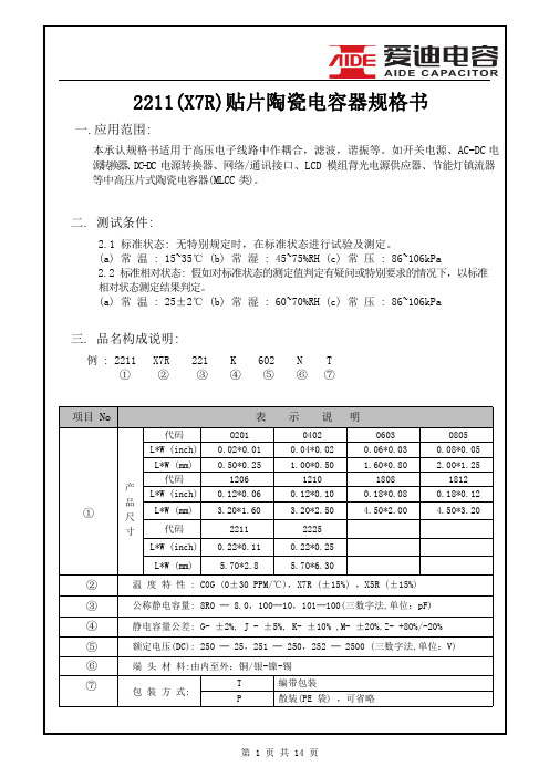
2 倍额定电压
电压 250V<V<1KV 1.5 倍额定电压
1KV≤V
1.2 倍额定电压
在常温常湿下放置 48±4 小时后再测试.
注:NO3,11,12,13 电容的初值测定:先放在 150℃预热 1 小时,再常温常压放置48 小时测试。
第 5 页 共 14 页
No 项 目
规格
测试方法
使用混合焊锡将电容器焊接在图1 的夹具(玻璃 环氧树脂)上,然后再图 2 所释放向加力. 焊接应 用回流焊进行,避免焊接不均及热冲击等不良 现象.
第 8 页 共 14 页
第 9 页 共 14 页
第 10 页 共 14 页
第 11 页 共 14 页
第 12 页 共 14 页
第 13 页 共 14 页
第 14 页 共 14 页
6
耐电压
无介质被击穿或损伤
Ur=450/500/630V,1.5倍额定电压
(DC)
1KV≤Ur≤2KV,........ 1.2倍额定电压
2KV<Ur,............... 1.1 倍额定电压 升压时间为:1~3S 保压时间为:5S
7
可焊性
■上锡率应大于 95% ■外观无可见损伤
将电容器在 80-120℃预热 10-30 秒,无铅焊料,使用 助焊剂;焊锡温度:245±5℃
测试电压:额定电压测
试时间:60±5 秒测试
5
绝缘电阻
IR≥4*109Ω,C≤25nF
湿度:≤75% 测试
IR*Cr≥100*1012Ω,C>25nF 温度:25±5℃
测试充放电电流:≤50mA
Ur=100V,............. 2.5 倍额定电压
Ur=200V/250V,.... 2.0 倍额定电压
HCPL-0211-500E中文资料

DescriptionThe HCPL-22XX, HCPL-02XX, and HCNW22XX are optical-ly-coupled logic gates. The HCPL-22XX, and HCPL-02XX contain a GaAsP LED while the HCNW22XX contains an AlGaAs LED. The detectors have totem pole output stag-es and optical receiver input stages with built-in Schmitt triggers t o p rovide l ogic-compatible w aveforms, e liminat-ing the need for additional waveshaping.A superior internal shield on the HCPL-2211/12, HCPL-0211, HCPL-2232 and HCNW2211 guarantees common mode transient immunity of 10 kV/µs at a common mode voltage of 1000 volts.Functional DiagramCAUTION: It is advised that normal static precautions be taken in handling and assembly of this component to prevent damage and/or degradation which may be induced by ESD.A 0.1 µF bypass capacitor must be connected between pins 5 and 8.NC ANODE CATHODE NC GNDV CC V O NC HCPL-2201/11HCPL-0201/11HCPL-2201 Functional Diagram NC ANODE CATHODE NC GNDV CC V O NC ANODE 1CATHODE 1CATHODE 2ANODE 2GNDV CC V O1V O2TRUTH TABLE (POSITIVE LOGIC)LED ON OFF V O HIGH LOWHCPL-2201, HCPL-2202, HCPL-2211,HCPL-2212, HCPL-2231, HCPL-2232, HCPL-0201, HCPL-0211, HCNW2201, HCNW2211Very High CMR, Wide V CC Logic Gate OptocouplersData SheetFeatures• 10 kV/µs minimum Common Mode Rejection(CMR) at V CM = 1000 V (HCPL-2211/2212/0211/2232, HCNW2211)• Wide operating V CC range: 4.5 to 20 Volts• 300 ns propagation delay guaranteed over the full temperature range• 5 Mbd typical signal rate• Low input current (1.6 mA to 1.8 mA)• Hysteresis• Totem pole output (no pullup resistor required)• Available in 8-Pin DIP , SOIC-8, widebody packages • Guaranteed performance from -40°C to 85°C • Safety approval– UL recognized -3750 V rms for 1 minute (5000 V rms for 1 minute for HCNW22XX) per UL1577– CSAapproved– IEC/EN/DIN EN 60747-5-2 approved with V IORM = 630 V peak (HCPL-2211/2212 Option 060 only) and V IORM = 1414 V peak (HCNW22XX only)• MIL-PRF-38534 hermetic version available (HCPL-52XX/62XX)Applications• Isolation of high speed logic systems• Computer-peripheral interfaces • Microprocessor system interfaces • Ground loop elimination• Pulse transformer replacement • High speed line receiver • Power control systemsSchematicHCPL-2201 SchematicHCPL-2201/02/11/12HCPL-0201/11HCNW2201/11V CCV OGNDV V CCV O1HCPL-2231/32V V O2GNDThe electrical and switching characteristics of the HCPL-22XX, HCPL-02XX and HCNW22XX are guaranteed from -40°C to +85°C and a V CC from 4.5 volts to 20 volts. Low I F and wide V CC range allow compatibility with TTL, LSTTL,and CMOS logic and result in lower power consumption compared to other high speed couplers. Logic signals are transmitted with a typical propagation delay of 150 ns.Small- Widebody Minimum CMR I nput 8-Pin DIP (300 Mil) Outline SO-8 (400 Mil) Hermetic On- Single Dual Single Single Single and dV/dt Current Channel Channel Channel Channel Dual Channel (V/µs) V CM (V) (mA) Package Package Package Package Packages1,000 50 1.6 HCPL-2200[1,2] HCPL-0201HCNW2201HCPL-2201 HCPL-2202 1.8 HCPL-22312,500 400 1.6 HCPL-2219[1,2] 5,000[3] 300[3] 1.6 HCPL-2211 HCPL-0211HCNW2211HCPL-2212 1,000 50 2.0 HCPL-52XX [2]HCPL-62XX [2]Notes:1. HCPL-2200/2219 devices include output enable/disable function.2. Technical data for the HCPL-2200/2219, HCPL-52XX and HCPL-62XX are on separate Avago publications.3. Minimum CMR of 10 kV/µs with V CM = 1000 V can be achieved with input current, I F , of 5 mA.Selection GuideOrdering InformationHCPL-2201, HCPL-2202, HCPL-2211, HCPL-2212, HCPL-2231, HCPL-2232, HCPL-0201, HCPL-0211 are UL Recognized with 3750 Vrms for 1 minute per UL1577.HCNW2201 and HCNW2211 are UL Recognized with 5000 Vrms for 1 minute per UL1577.All devices listed above are approved under CSA Component Acceptance Notice #5, File CA 88324.Part numberOptionPackageSurfaceMountGullWingTape &ReelUL 5000Vrms/ 1MinuteratingIEC/EN/DIN EN60747-5-2Quantity RoHSCompliantNon RoHSCompliantHCPL-2201 HCPL-2202 HCPL-2211 HCPL-2212-000E No option300milDIP-850 per tube -300E-300 X X50 per tube -500E-500X X X1000 per reel -060E-060X50 per tube -360E-360X X X50 per tube -560E-560X X X X1000 per reelHCPL-2231 HCPL-2232-000E No option50 per tube -300E-300 X X50 per tube -500E-500X X X1000 per reelHCPL-0201 HCPL-0211-000E No optionSO-8100 per tube -500E-500X X X1500 per reel -060E-060X100 per tube -560E-560X X X X1500 per reelHCNW2201 HCNW2211-000E No option400milWidebodyDIP-842 per tube -300E-300 X X42 per tube -500E-500X X X750 per reelTo order, choose a part number from the part number column and combine with the desired option from the option column to form an order entry.Example 1:HCPL-2202-560E to order product of 300mil DIP Gull Wing Surface Mount package in Tape and Reel packaging with IEC/EN/DIN EN 60747-5-2 Safety Approval in RoHS compliant.Example 2:HCPL-2202 to order product of 300mil DIP package in tube packaging and non RoHS compliant.Option datasheets are available. Contact your Avago sales representative or authorized distributor for information. Remarks: The notation ‘#XXX’ is used for existing products, while (new) products launched since 15th July 2001 and RoHS compliant option will use ‘-XXXE‘.Package Outline Drawings8-Pin DIP Package (HCPL-2201/02/11/12/31/32)8-Pin DIP Package with Gull Wing Surface Mount Option 300 (HCPL-2201/02/11/12/31/32)+ 0.076- 0.051(0.010+ 0.003)- 0.002)DIMENSIONS IN MILLIMETERS AND (INCHES).UR * MARKING CODE LETTER FOR OPTION NUMBERS "V" = OPTION 060OPTION NUMBERS 300 AND 500 NOT MARKED.NOTE: FLOATING LEAD PROTRUSION IS 0.25 mm (10 mils) MAX.1.080 ± 0.320(0.100)BSCDIMENSIONS IN MILLIMETERS (INCHES).LEAD COPLANARITY = 0.10 mm (0.004 INCHES).NOTE: FLOATING LEAD PROTRUSION IS 0.25 mm (10 mils) MAX.+ 0.076- 0.051+ 0.003)- 0.002)Small-Outline SO-8 Package (HCPL-0201/11)8-Pin Widebody DIP Package (HCNW2201/11)(0.012)MIN.5.207 ± 0.254 (0.205 ± 0.010)DIMENSIONS IN MILLIMETERS (INCHES).LEAD COPLANARITY = 0.10 mm (0.004 INCHES) MAX.NOTE: FLOATING LEAD PROTRUSION IS 0.15 mm (6 mils) MAX.*1.78 ± 0.15(0.070 ± 0.006)TYP.NOTE: FLOATING LEAD PROTRUSION IS 0.25 mm (10 mils) MAX.+ 0.076- 0.0051+ 0.003)- 0.002)8-Pin Widebody DIP Package with Gull Wing Surface Mount Option 300 (HCNW2201/11)Solder Reflow Temperature Profile1.78 ± 0.15(0.070 ± 0.006)MAX.BSCDIMENSIONS IN MILLIMETERS (INCHES).LEAD COPLANARITY = 0.10 mm (0.004 INCHES).NOTE: FLOATING LEAD PROTRUSION IS 0.25 mm (10 mils) MAX.TIME (SECONDS)T E M P E R A T U R E (°C )ROOM TEMPERATURENOTE:NON-HALIDE FLUX SHOULD BE USED.Regulatory InformationThe HCPL-22XX/02XX and HCNW22XX have been approved by the following organizations:ULRecognized under UL 1577, Component Recognition Program, File E55361.CSAApproved under CSA Component Acceptance Notice #5, File CA 88324.IEC/EN/DIN EN 60747-5-2Approved under:IEC 60747-5-2:1997 + A1:2002 EN 60747-5-2:2001 + A1:2002DIN EN 60747-5-2 (VDE 0884 Teil 2):2003-01(Option 060 and HCNW only)Recommended Pb-Free IR ProfileInsulation and Safety Related Specifications 8-pin DIP Package 8-Pin DIP Widebody (300 Mil) SO-8 (400 Mil) Parameter Symbol ValueValueValueUnitsConditionsMinimum External L(101) 7.1 4.9 9.6 mm Measured from input terminals Air Gap (External to output terminals, shortest Clearance) distance through air.Minimum External L(102) 7.4 4.8 10.0 mm Measured from input terminals Tracking (External to output terminals, shortest Creepage) distance path along body. Minimum Internal 0.08 0.08 1.0 mm Through insulation distance, Plastic Gapconductor to conductor, usually (Internal Clearance) the direct distance between the photoemitter and photodetectorinside the optocoupler cavity. Minimum Internal NA NA 4.0 mm Measured from input terminals Tracking (Internal to output terminals, along Creepage) internal cavity.Tracking Resistance CTI200200200VoltsDIN IEC 112/VDE 0303 Part 1(Comparative Tracking Index) Isolation Group IIIa IIIa IIIa Material Group(DIN VDE 0110, 1/89, Table 1)Option 300 - surface mount classification is Class A in accordance with CECC 00802.T LT smax T smin25T p TIMET E M P E R A T U R ENOTES:THE TIME FROM 25°C to PEAK TEMPERATURE =8MINUTES MAX.T smax =200°C,T smin =150°CNOTE:NON-HALIDE FLUX SHOULD BE USED.*RECOMMENDED PEAK TEMPERATUREFOR WIDEBODY 400mils PACKAGE IS 245°C(HCPL-2211/2212 Option 060 ONLY) DescriptionSymbolCharacteristicUnitsInstallation classification per DIN VDE 0110/1.89, Table 1 Climatic Classification55/85/21Pollution Degree (DIN VDE 0110/1.89) 2 Maximum Working Insulation VoltageV IORM 630 V peak Input to Output Test Voltage, Method b*V IORM x 1.875 = V PR , 100% Production Test with t m = 1 sec, V PR1181V peakPartial Discharge < 5 pCInput to Output Test Voltage, Method a* V IORM x 1.5 = V PR , Type and sample test, V PR945V peakt m = 60 sec, Partial Discharge < 5 pC Highest Allowable Overvoltage* (Transient Overvoltage, t ini = 10 sec) V IOTM6000V peakSafety Limiting Values(Maximum values allowed in the event of a failure, also see Figure 12, Thermal Derating curve.) Case Temperature T S175 °C Input Current I S,OUTPUT 230 mAOutput PowerP S,OUTPUT 600 mW Insulation Resistance at T S , V IO = 500 VR S≥109Ω*Refer to the front of the optocoupler section of the current catalog, under Product Safety Regulations section IEC/EN/DIN EN 60747-5-2, for a detailed description.Note: Isolation characteristics are guaranteed only within the safety maximum ratings which must be ensured by protective circuits in applica-tion.(HCNW22XX ONLY) DescriptionSymbolCharacteristicUnitsfor rated mains voltage ≤600 V rms I-IV Climatic Classification55/100/21Pollution Degree (DIN VDE 0110/1.89) 2 Maximum Working Insulation VoltageV IORM 1414 V peak Input to Output Test Voltage, Method b*V IORM x 1.875 = V PR , 100% Production Test with t m = 1 sec, V PR2652V peakPartial Discharge < 5 pCInput to Output Test Voltage, Method a* V IORM x 1.5 = V PR , Type and sample test, V PR2121V peakt m = 60 sec, Partial Discharge < 5 pC Highest Allowable Overvoltage* (Transient Overvoltage, t ini = 10 sec) V IOTM8000V peakSafety Limiting Values(Maximum values allowed in the event of a failure, also see Figure 12, Thermal Derating curve.) Case TemperatureT S150 °C Current (Input Current I F , P S = 0) I S,INPUT 400 mAOutput PowerP S,OUTPUT 700 mW Insulation Resistance at T S , V IO = 500 VR S≥109Ω*Refer to the front of the optocoupler section of the current catalog, under Product Safety Regulations section IEC/EN/DIN EN 60747-5-2, for a detailed description.Note: Isolation characteristics are guaranteed only within the safety maximum ratings which must be ensured by protective circuits in applica-tion.Absolute Maximum RatingsParameter Symbol Min. Max. Units Note-55 125 °CStorage Temperature TS-40 85 °C Operating Temperature TA10 mA 1 Average Forward Input Current IF(AVG)Peak Transient Input Current< 1% Duty Cycle)25 mA 1 Average Output Current IOSupply Voltage V0 20 VCCOutput Voltage V-0.5 20 V 1OOutput Power Dissipation PSee Figure 7 1OLead Solder Temperature (Through Hole Parts Only) 260°C for 10 sec.,Solder Reflow Temperature Profile See Package Outline Drawings section(Surface Mount Parts Only)Recommended Operating ConditionsParameter Symbol Min. Max. Units Power Supply Voltage V4.5 20 VCCForward Input Voltage (OFF) V- 0.8 VF(OFF)-40 85 °C Operating Temperature TAJunction Temperature T-40 125 °CJFan Out N 4 TTL Loads*The initial switching threshold is 1.6 mA or less. It is recommended that 2.2 mA be used to permit at least a 20% LED degradation guardband.†The initial switching threshold is 1.8 mA or less. It is recommended that 2.5 mA be used to permit at least a 20% LED degradation guardband.Electrical Specifications-40°C ≤ T A ≤ 85°C, 4.5 V ≤ V CC ≤ 20 V, 1.6 mA ≤ I F(ON)* ≤ 5 mA, 0 V ≤ V F(OFF) ≤ 0.8 V, unless otherwise specified.All Typicals at T A = 25°C. See Note 7. ParameterSym.Min.Typ.Max.UnitsTest Conditions F ig.NoteLogic Low Output Voltage V OL 0.5 V I OL = 6.4 mA (4 TTL Loads) 1, 3 1Input Reverse Breakdown BV 5 V I = 10 µA 1*For HCPL-223X, 1.8 mA ≤ I F(ON) ≤ 5 mA.**Typical V OH = V CC - 2.1 V.ParameterSym.DeviceMin.UnitsTest Conditions Fig.NoteLogic High|CM H | HCPL-2201/02 1,000 V/µs |V CM | = 50 V V CC = 5 V 101, 7Common Mode HCPL-0201I F = 1.6 mA †T A = 25°CTransient HCPL-2231CM HCNW2211 I F = 5.0 mA Logic Low|CM L | HCPL-2201/02 1,000 V/µs |V CM | = 50 V V F = 0 V 101, 7Common Mode HCPL-0201 V CC = 5 V Transient HCPL-2231T = 25°CHCPL-2232HCNW2211*For HCPL-223X, 1.8 mA ≤ I F(ON) ≤ 5 mA.†I F = 1.8 mA for HCPL-2231.‡I F = 1.8 mA for HCPL-2232.Switching Specifications (AC)-40°C ≤ T A ≤ 85°C, 4.5 V ≤ V CC ≤ 20 V, 1.6 mA ≤ I F(ON)* ≤ 5 mA, 0 V ≤ V F(OFF) ≤ 0.8 V.All Typicals at T A = 25°C, V CC = 5 V, I F(ON) = 3 mA unless otherwise specified. ParameterSym.Min.Typ.Max.UnitsTest ConditionsFig.NotePropagation Delay Time t 110 ns Without Peaking Capacitor 5, 6 1, 6Output Rise Time (10-90%) t r 30 ns 5, 9 1 Output Fall Time (90-10%)t f7ns5, 91Notes:1. Each channel.2. Derate total package power dissipation, P T , linearly above 70°C free-air temperature at a rate of 4.5 mW/°C.3. Duration of output short circuit time should not exceed 10 ms.4. For single devices, input capacitance is measured between pin 2 and pin 3.5. Device considered a two-terminal device: pins 1, 2, 3, and 4 shorted together and pins 5, 6, 7, and 8 shorted together.6. The t PLH propagation delay is measured from the 50% point on the leading edge of the input pulse to the 1.3 V point on the leading edge ofthe output pulse. The t PHL propagation delay is measured from the 50% point on the trailing edge of the input pulse to the 1.3 V point on the trailing edge of the output pulse.7. CM H is the maximum slew rate of the common mode voltage that can be sustained with the output voltage in the logic high state, V O > 2.0 V.CM L is the maximum slew rate of the common mode voltage that can be sustained with the output voltage in the logic low state, V O < 0.8 V. 8. For HCPL-2202/12, V O is on pin 6.9. Use of a 0.1 µF bypass capacitor connected between pins 5 and 8 is recommended.10. In accordance with UL 1577, each optocoupler is proof tested by applying an insulation test voltage ≥4500 V rms for one second (leakagedetection current limit, I I-O ≤5 µA). This test is performed before the 100% production test for partial discharge (Method b) shown in the IEC/EN/DIN EN 60747-5-2 Insulation Characteristics Table, if applicable.11. In accordance with UL 1577, each optocoupler is proof tested by applying an insulation test voltage ≥6000 V rms for one second (leakagedetection current limit, I I-O ≤5 µA). This test is performed before the 100% production test for partial discharge (Method b) shown in the IEC/EN/DIN EN 60747-5-2 Insulation Characteristics Table.12. For HCPL-2231/32 only. Measured between pins 1 and 2, shorted together, and pins 3 and 4, shorted together.Package Characteristics ParameterSym.Min.Typ.Max.UnitsTest ConditionsFig.Note12A Input-Input Insulation I I-I0.005 µA Relative Humidity = 45%, 12 Leakage Current t = 5 s, V I-I = 500 V Resistance (Input-Input) R I-I 1011 Ω V I-I = 500 V 12 Capacitance (Input-Input)C I-I0.25pFf = 1 MHz12*The Input-Output Momentary Withstand Voltage is a dielectric voltage rating that should not be interpreted as an input-output continuousvoltage rating. For the continuous voltage rating refer to the IEC/EN/DIN EN 60747-5-2 Insulation Characteristics Table (if applicable), your equip-ment level safety specification or Avago Application Note 1074 entitled “Optocoupler Input-Output Endurance Voltage,” publication number 5963-2203I O H – H I G H L E V E L O U T P U T C U R R E N T – m A-8T A – TEMPERATURE – °C HCPL-2201 fig 2-5-3-1-6-7-4-2V O – O U T P U T V O L T A G E– VI F – INPUT CURRENT – mAHCPL-2201 fig 3Figure 1. Typical logic low output voltage vs. tem-perature.Figure 2. Typical logic high output current vs. tem-perature.Figure 3. Typical output voltage vs. forward input current.I F – F O R W A R D C U R R E N T – m A0.001V F – FORWARD VOLTAGE – V 1.0HCPL-2201 fig 4a10000.010.110100HCPL-22XX I F – F O R W A R D C U R R E NT – m A0.001V F – FORWARD VOLTAGE – V1.0HCPL-2201 fig 4b10000.010.110100Figure 4. Typical input diode forward characteristic.Figure 5. Circuit for t PLH , t PHL , t r , t f .HCPL-2201 fig 5aΩARE INCLUDED IN C 1 AND C 2.D 2D 3D 4R 1I F (ON)2.15 k Ω1.6 mA 1.10 k Ω3 mA681 Ω5 mA ALL DIODES ARE 1N916 OR 1N3064.HCPL-2201 fig 5bΩARE INCLUDED IN C 1 AND C 2.D 2D 3D 4R 1I F (ON)1.96 k Ω1.8 mA 1.10 k Ω3 mA681 Ω5 mA ALL DIODES ARE 1N916 OR 1N3064.F (ON)OL* 0.1 µF BYPASS — SEE NOTE 9.V O L – L O W L E V E L O U T P U T V O L T A G E – VT A – TEMPERATURE – °CHCPL-2201 fig 11.00.40.60.80.20.10.30.50.70.9t P – P R O P A G A T I O N D E L A Y – n s50T A – TEMPERATURE – °C 200HCPL-2201 fig 6b250100150Figure 6. Typical propagation delays vs. temperature.Figure 7. Maximum output power per channel vs. sup-ply voltage.V O H – H I G H L E V E LO U T P U T V O L T A G E – VV CC – SUPPLY VOLTAGE – V 15HCPL-2201 fig 820510t r , t f – R I S E , F A L LT I M E – n sT A – TEMPERATURE – °CHCPL-2201 fig 910040608020Figure 8. Typical logic high output voltage vs. supply voltage.Figure 9. Typical rise, fall time vs. temperature.Figure 10. Test circuit for common mode transient immunity and typical waveforms.V CM (PEAK)OUTPUT V O * SEE NOTE 7, 9.** I F = 1.8 mA FOR HCPL-2231/32 DEVICES.0 V V OH|V CM |V OLV O (MAX.)*V O (MIN.)*SWITCH AT A: I F = 1.6 mA**SWITCH AT B: V F = 0 V CM(PEAK)OUTPUT V O * SEE NOTE 7, 9.** I F = 1.8 mA FOR HCPL-2231/32 DEVICES.0 VV OH|V CM |V OL V O (MAX.)*V O (MIN.)*SWITCH AT A: I F = 1.6 mA**F = 0 V t P – P R O P AG A T I O N D E L A Y – n sT A – TEMPERATURE – °C HCPL-2201 fig 6aHCPL-22XX P O – M A X I M U M O U T P U T P O W E R P E R C H A N N E L (m W )V CC – SUPPLY VOLTAGE – V60HCPL-2201 fig 7802040HCPL-2201/11HCPL-02XX HCPL-2201 fig 10aO R V FFHCPL-2201 fig 10bO V FFO U T P U T P O W E R – P S , I N P U T C U R R E N T – I S0T S – CASE TEMPERATURE – °C 400600800200100300500700Figure 11. Typical input threshold current vs. temperature.Figure 12. Thermal derating curve, dependence of safety limiting value with case temperature per IEC/EN/DIN EN 60747-5-2.Figure 13a. Recommended LSTTL to LSTTL circuit where 500 ns propagation delay is sufficient.HCPL-2201 fig 13aHCPL-2201/11HCPL-02XX DATA INPUTV CC2 (+5 V)UP TO 16 LSTTL LOADS OR 4 TTL LOADSV CC1DATA OUTPUTI N P U T C U R R E N T T H R E S H O L D – m A0.5T A – TEMPERATURE – °C HCPL-2201 fig 11a1.00.70.80.90.6HCPL-22XXI N P U T C U R R E N T T H R E S H O L D – m AT A – TEMPERATURE – °CHCPL-2201 fig 11bHCNW22XX O U T P U T P O W E R P S , I N P U T C U R R E N T I ST S – CASE TEMPERATURE – °CHCPL-2201 fig 12bFigure 16. Series LED drive with open collector gate (4.7 k resistor shunts I OH from the LED).Figure 14. LSTTL to CMOS interface circuit.HCPL-2201 fig 15HCPL-2201/11HCPL-02XX V CC1Figure 15. Alternative LED drive circuit.HCPL-2201/11HCPL-02XX V CC RESISTOR MAY BE SHORTED WHERE 500 ns PROPAGATION DELAY IS SUFFICIENT.Figure 13b. Recommended LSTTL to LSTTL circuit for applications requiring a maximum allowable propagation delay of 300 ns.HCPL-2201 fig 13bHCPL-2201/11HCPL-02XX DATA INPUTV CC2 (+5 V)UP TO 16 LSTTL LOADS OR 4 TTL LOADSV CC1 DATA OUTPUTHCPL-2201 fig 14V CC2 **0.1 µF BYPASSV CC1 DATA OUTPUTΩRESISTOR MAY BE SHORTED WHERE 500 ns PROPAGATION DELAY IS SUFFICIENT.10 V 15 V 20 V 2.37 k Ω3.83 k Ω5.11 k ΩFor product information and a complete list of distributors, please go to our website: Avago, Avago Technologies, and the A logo are trademarks of Avago Technologies Limited in the United States and other countries. Data subject to change. Copyright © 2005-2008 Avago Technologies Limited. All rights reserved. Obsoletes AV01-0556ENAV02-0674EN - June 20, 2008。
- 1、下载文档前请自行甄别文档内容的完整性,平台不提供额外的编辑、内容补充、找答案等附加服务。
- 2、"仅部分预览"的文档,不可在线预览部分如存在完整性等问题,可反馈申请退款(可完整预览的文档不适用该条件!)。
- 3、如文档侵犯您的权益,请联系客服反馈,我们会尽快为您处理(人工客服工作时间:9:00-18:30)。
1-131HVery High CMR, Wide V CC Logic Gate Optocouplers Technical DataHCPL-2201HCPL-2202HCPL-2211HCPL-2212HCPL-2231HCPL-2232HCPL-0201HCPL-0211HCNW2201HCNW2211Features• 10 kV/µs Minimum Common Mode Rejection (CMR) at V CM = 1000 V(HCPL-2211/2212/0211/2232, HCNW2211)• Wide Operating V CC Range:4.5 to 20 Volts• 300 ns Propagation Delay Guaranteed over the Full Temperature Range• 5 Mbd Typical Signal Rate • Low Input Current (1.6mA to 1.8 mA)• Hysteresis• Totem Pole Output (No Pullup Resistor Required)• Available in 8-Pin DIP,SOIC-8, Widebody Packages • Guaranteed Performance from -40°C to 85°C • Safety ApprovalUL Recognized -2500 V rms for 1 minute (5000V rms for 1 minute forHCNW22XX) per UL1577CSA ApprovedVDE 0884 Approved with V IORM = 630 V peak (HCPL-2211/2212 Option 060 only)and V IORM = 1414 V peak (HCNW22XX only)BSI Certified (HCNW22XX only)• MIL-STD-1772 Version Available(HCPL-52XX/62XX)Applications• Isolation of High Speed Logic Systems• Computer-Peripheral Interfaces• Microprocessor System Interfaces• Ground Loop Elimination • Pulse Transformer Replacement• High Speed Line Receiver • Power Control SystemsDescriptionThe HCPL-22XX, HCPL-02XX,and HCNW22XX are optically-coupled logic gates. TheHCPL-22XX, and HCPL-02XX contain a GaAsP LED while the HCNW22XX contains an AlGaAs LED. The detectors have totem pole output stages and optical receiver input stages with built-in Schmitt triggers to provide logic-compatible waveforms, eliminat-ing the need for additional waveshaping.A superior internal shield on the HCPL-2211/12, HCPL-0211,CAUTION: It is advised that normal static precautions be taken in handling and assembly of this componentto prevent damage and/or degradation which may be induced by ESD.Functional DiagramA 0.1 µF bypass capacitor must be connected between pins 5 and 8.NC ANODE CATHODE NC GNDV CC V O NC HCPL-2201/11 HCPL-0201/11NC ANODE CATHODE NC GNDV CC V O NCANODE 1CATHODE 1CATHODE 2ANODE 2GNDV CC V O1V O2TRUTH TABLE (POSITIVE LOGIC)LED ON OFF V O HIGH LOW5965-3595ESelection GuideNotes:1. HCPL-2200/2219 devices include output enable/disable function.2. Technical data for the HCPL-2200/2219, HCPL-52XX and HCPL-62XX are on separate HP publications.3. Minimum CMR of 10 kV/µs with V CM = 1000 V can be achieved with input current, I F, of 5 mA.Ordering InformationSpecify Part Number followed by Option Number (if desired).Example:HCPL-2211#XXX060 = VDE 0884 V IORM = 630 V peak Option*300 = Gull Wing Surface Mount Option**500 = Tape and Reel Packaging OptionOption data sheets available. Contact your Hewlett-Packard sales representative or authorized distributor for information.*For HCPL-2211/2212 only.**Gull wing surface mount option applies to through hole parts only.SchematicHCPL-2201/02/11/12HCPL-0201/11HCNW2201/11V CCV OGNDVV CCV O1HCPL-2231/32VV O2GNDHCPL-2232 and HCNW2211guarantees common modetransient immunity of 10 kV/µs ata common mode voltage of 1000volts.The electrical and switchingcharacteristics of the HCPL-22XX, HCPL-02XX andHCNW22XX are guaranteed from-40°C to +85°C and a V CC from4.5 volts to 20 volts. Low I F andwide V CC range allow compatibil-ity with TTL, LSTTL, and CMOSlogic and result in lower powerconsumption compared to otherhigh speed couplers. Logic signalsare transmitted with a typicalpropagation delay of 150ns.1-1320.254+ 0.076- 0.051(0.010+ 0.003)- 0.002)DIMENSIONS IN MILLIMETERS AND (INCHES).*MARKING CODE LETTER FOR OPTION NUMBERS"V" = OPTION 060OPTION NUMBERS 300 AND 500 NOT MARKED. Package Outline Drawings8-Pin DIP Package (HCPL-2201/02/11/12/31/32)8-Pin DIP Package with Gull Wing Surface Mount Option 300 (HCPL-2201/02/11/12/31/32)MAX.(0.100)BSCDIMENSIONS IN MILLIMETERS (INCHES).LEAD COPLANARITY = 0.10 mm (0.004 INCHES).+ 0.076- 0.051+ 0.003)- 0.002)1-133Small-Outline SO-8 Package (HCPL-0201/11) 8-Pin Widebody DIP Package (HCNW2201/11)1.78 ± 0.15+ 0.076- 0.0051+ 0.003)- 0.002)(0.012)MIN.DIMENSIONS IN MILLIMETERS (INCHES).LEAD COPLANARITY = 0.10 mm (0.004 INCHES).1-1341-1358-Pin Widebody DIP Package with Gull Wing Surface Mount Option 300 (HCNW2201/11)Note: Use of nonchlorine activated fluxes is highly recommended.240TIME – MINUTEST E M P E R A T U R E – °C220200180160140120100806040200260Solder Reflow Temperature Profile (HCPL-02XX and Gull Wing Surface Mount Option 300 Parts)1.78 ± 0.15 MAX.BSCDIMENSIONS IN MILLIMETERS (INCHES).LEAD COPLANARITY = 0.10 mm (0.004 INCHES).Regulatory Information The HCPL-22XX/02XX and HCNW22XX have been approved by the following organizations: ULRecognized under UL 1577, Component Recognition Program, File E55361.CSAApproved under CSA ComponentAcceptance Notice #5, File CA88324.VDEApproved according to VDE0884/06.92. (HCPL-2211/2212Option 060 and HCNW22XX only)BSICertification according toBS415:1994,(BS EN60065:1994);BS EN60950:1992(BS7002:1992) andEN41003:1993 for Class IIapplications. (HCNW22XX only)Insulation and Safety Related Specifications8-pin DIP Package8-Pin DIP Widebody(300 Mil)SO-8(400 Mil)Parameter Symbol Value Value Value Units Conditions Minimum External L(101)7.1 4.99.6mm Measured from input terminals Air Gap (External to output terminals, shortest Clearance)distance through air. Minimum External L(102)7.4 4.810.0mm Measured from input terminals Tracking (External to output terminals, shortest Creepage)distance path along body. Minimum Internal0.080.08 1.0mm Through insulation distance, Plastic Gap conductor to conductor, usually (Internal Clearance)the direct distance between thephotoemitter and photodetectorinside the optocoupler cavity. Minimum Internal NA NA 4.0mm Measured from input terminals Tracking (Internal to output terminals, along Creepage)internal cavity.Tracking Resistance CTI200200200Volts DIN IEC 112/VDE 0303 Part 1 (ComparativeTracking Index)Isolation Group IIIa IIIa IIIa Material Group(DIN VDE 0110, 1/89, Table 1) Option 300 - surface mount classification is Class A in accordance with CECC 00802.1-136VDE 0884 Insulation Related Characteristics(HCPL-2211/2212 Option 060 ONLY)*Refer to the front of the optocoupler section of the current catalog, under Product Safety Regulations section (VDE 0884), for a detailed description.Note: Isolation characteristics are guaranteed only within the safety maximum ratings which must be ensured by protective circuits in application.1-137VDE 0884 Insulation Related Characteristics (HCNW22XX ONLY)*Refer to the front of the optocoupler section of the current catalog, under Product Safety Regulations section (VDE 0884), for a detailed description.Note: Isolation characteristics are guaranteed only within the safety maximum ratings which must be ensured by protective circuits in application.Absolute Maximum Ratings1-138*The initial switching threshold is 1.6 mA or less. It is recommended that 2.2 mA be used to permit at least a 20% LED degradation guardband.†The initial switching threshold is 1.8 mA or less. It is recommended that 2.5 mA be used to permit at least a 20% LED degradation guardband.Electrical Specifications-40°C ≤ T A≤ 85°C, 4.5 V ≤ V CC≤ 20 V, 1.6 mA ≤ I F(ON)* ≤ 5 mA, 0 V ≤ V F(OFF)≤ 0.8 V, unless otherwise specified. All Typicals at T A = 25°C. See Note 7.*For HCPL-223X, 1.8 mA ≤ I F(ON)≤ 5 mA.**Typical V OH = V CC - 2.1 V.1-139Switching Specifications (AC)-40°C ≤ T A≤ 85°C, 4.5 V ≤ V CC≤ 20 V, 1.6 mA ≤ I F(ON)*≤ 5 mA, 0 V ≤ V F(OFF)≤ 0.8 V. All Typicals at T A = 25°C, V CC = 5 V, I F(ON) = 3 mA unless otherwise specified.*For HCPL-223X, 1.8 mA ≤ I F(ON)≤ 5 mA.†I F = 1.8 mA for HCPL-2231.‡I F = 1.8 mA for HCPL-2232.1-140Package Characteristics*The Input-Output Momentary Withstand Voltage is a dielectric voltage rating that should not be interpreted as an input-output continuous voltage rating. For the continuous voltage rating refer to the VDE 0884 Insulation Characteristics Table (if applicable), your equipment level safety specification or HP Application Note 1074 entitled “Optocoupler Input-Output Endurance Voltage,”publication number 5963-2203E.Notes:1. Each channel.2. Derate total package power dissipation, P T, linearly above 70°C free-air temperature at a rate of 4.5 mW/°C.3. Duration of output short circuit time should not exceed 10 ms.4. For single devices, input capacitance is measured between pin 2 and pin 3.5. Device considered a two-terminal device: pins 1, 2, 3, and 4 shorted together and pins 5, 6, 7, and 8 shorted together.6. The t PLH propagation delay is measured from the 50% point on the leading edge of the input pulse to the 1.3 V point on theleading edge of the output pulse. The t PHL propagation delay is measured from the 50% point on the trailing edge of the input pulse to the 1.3 V point on the trailing edge of the output pulse.7. CM H is the maximum slew rate of the common mode voltage that can be sustained with the output voltage in the logic high state,V O > 2.0 V. CM L is the maximum slew rate of the common mode voltage that can be sustained with the output voltage in the logic low state, V O < 0.8 V.8. For HCPL-2202/12, V O is on pin 6.9. Use of a 0.1 µF bypass capacitor connected between pins 5 and 8 is recommended.10. In accordance with UL 1577, each optocoupler is proof tested by applying an insulation test voltage ≥3000 V rms for one second(leakage detection current limit, I I-O≤5 µA). This test is performed before the 100% production test for partial discharge (Methodb) shown in the VDE 0884 Insulation Characteristics Table, if applicable.11. In accordance with UL 1577, each optocoupler is proof tested by applying an insulation test voltage ≥6000 V rms for one second(leakage detection current limit, I I-O≤5 µA). This test is performed before the 100% production test for partial discharge (Methodb) shown in the VDE 0884 Insulation Characteristics Table.12. For HCPL-2231/32 only. Measured between pins 1 and 2, shorted together, and pins 3 and 4, shorted together.1-1411-142I O H – H I G H L E V E L O U T P U T C U R R E N T – m A-8T A – TEMPERATURE – °C 0-5-3-1-6-7-4-2V O – O U T P U T V O L T A G E –VI F – INPUT CURRENT – mAFigure 1. Typical Logic Low Output Voltage vs. Temperature.Figure 2. Typical Logic High Output Current vs. Temperature.Figure 3. Typical Output Voltage vs.Forward Input Current.I F – F O R W A R D C U R R E N T – m AV F – FORWARD VOLTAGE – VHCPL-22XX I F – F O R W A R D C U R R E N T – m AV F – FORWARD VOLTAGE – VFigure 4. Typical Input Diode Forward Characteristic.Figure 5. Circuit for t PLH , t PHL , t r ,t f .ΩARE INCLUDED IN C 1 AND C 2.D 2D 3D 4R 1I F (ON)2.15 k Ω 1.6 mA 1.10 k Ω 3 mA681 Ω 5 mA ALL DIODES ARE 1N916 OR 1N3064.ΩARE INCLUDED IN C 1 AND C 2.D 2D 3D 4R 1I F (ON)1.96 k Ω 1.8 mA 1.10 k Ω 3 mA681 Ω 5 mA ALL DIODES ARE 1N916 OR 1N3064.F (ON)V OL* 0.1 µF BYPASS — SEE NOTE 9.V O L – L O W L E V E L O U T P U T V O L T A G E – VT A – TEMPERATURE – °C1-143t P – P R O P A G A T I O N D E L A Y – n s50T A – TEMPERATURE – °C 200250100150Figure 6. Typical Propagation Delays vs. Temperature.Figure 7. Maximum Output Power per Channel vs. Supply Voltage.V O H – H I G H L E VE L O U T P U T V O L T A G E – VV CC – SUPPLY VOLTAGE – V 1520510t r , t f – R I S E , F A L LT I M E – n sT A – TEMPERATURE – °CFigure 8. Typical Logic High Output Voltage vs. Supply Voltage.Figure 9. Typical Rise, Fall Time vs.Temperature.Figure 10. Test Circuit for Common Mode Transient Immunity and Typical Waveforms.V CM (PEAK)OUTPUT V O0 VV OH|V CM |V OLV O (MAX.)*V O (MIN.)*SWITCH AT A: I F = 1.6 mA**SWITCH AT B: V F = 0 V* SEE NOTE 7, 9.** I F = 1.8 mA FOR HCPL-2231/32 DEVICES.t P – P R O P A G A T I O N D E L AY – n s50T A – TEMPERATURE – °C 200250100150HCPL-22XX HCPL-02XXP O – M A X I M U M O U T P U T P O W E R P E R C H A NN E L (m W )V CC – SUPPLY VOLTAGE – VHCPL-2201/11 HCPL-02XX O R V FFO V FF1-144O U T P U T P O W E R – P S , I N P U T C U R R E N T – I S0T S – CASE TEMPERATURE – °C 400600800200100300500700Figure 11. Typical Input Threshold Current vs. Temperature.Figure 12. Thermal Derating Curve, Dependence of Safety Limiting Value with Case Temperature per VDE 0884.Figure 13a. Recommended LSTTL to LSTTL Circuit where 500 ns Propagation Delay is Sufficient.HCPL-2201/11 HCPL-02XX DATA INPUTV CC2 (+5 V)UP TO 16 LSTTL LOADS OR 4 TTL LOADSV CC1DATA OUTPUTI N P U T C U R R E N T T H R E S H O L D – m A0.5T A – TEMPERATURE – °C 1.00.70.80.90.6HCPL-22XXI N P U T C U R R E N T T H R E S H O L D – m AT A – TEMPERATURE – °CHCNW22XXO U T P U T P O W E R P S , I N P U T C U R R E N T I S0T S – CASE TEMPERATURE – °C1000400600800200100300500700900HCNW22XX1-145Figure 16. Series LED Drive with Open Collector Gate (4.7k Resistor Shunts I OH from the LED).Figure 14. LSTTL to CMOS Interface Circuit.HCPL-2201/11 HCPL-02XX V CC1Figure 15. Alternative LED Drive Circuit.HCPL-2201/11 HCPL-02XX DATA INPUTV CC RESISTOR MAY BE SHORTED WHERE 500 ns PROPAGATION DELAY IS SUFFICIENT.Figure 13b. Recommended LSTTL to LSTTL Circuit for Applications Requiring a Maximum Allowable Propagation Delay of 300 ns.HCPL-2201/11 HCPL-02XX DATA INPUTV CC2 (+5 V)UP TO 16 LSTTL LOADS OR 4 TTL LOADSV CC1 DATA OUTPUTDATA INPUTV CC2 **0.1 µF BYPASSV DATA OUTPUTMAY BE OMITTED AND 80 ΩRESISTOR MAY BE SHORTED WHERE 500 ns PROPAGATION DELAY IS SUFFICIENT.10 V 15 V 20 V 2.37 k Ω3.83 k Ω5.11 k Ω。