OMAP35x Peripherals Overview Reference Guide
PSD4235G2-70U;PSD4235G2-90U;PSD4235G2-90UI;中文规格书,Datasheet资料
February 2009 Rev 41/129PSD4235G2Flash in-system programmable (ISP)for 16-bit MCUs (5 V supply)Features■Dual bank Flash memories– 4 Mbit of Primary Flash memory (8 uniform sectors, 32K x 16)–256 Kbit Secondary Flash memory with 4 sectors–Concurrent operation: read from onememory while erasing and writing the other ■64 Kbit SRAM■PLD with macrocells–Over 3000 gates of PLD: CPLD and DPLD –CPLD with 16 output macrocells (OMCs) and 24 input macrocells (IMCs)–DPLD - user defined internal chip select decoding ■7 L/O ports with 52 I/O pins–52 individually configurable I/O port pins that can be used for the following functions:–MCU I/Os –PLD I/Os–Latched MCU address output –Special function l/Os–l/O ports may be configured as open-drain outputs ■In-system programming (ISP) with JTAG –Built-in JTAG compliant serial port allows full-chip In-System Programmability–Efficient manufacturing allow easy product testing and programmingUse low cost FlashLINK cable with PC■Page register–Internal page register that can be used to expand the microcontroller address space by a factor of 256–Programmable power management ●High endurance–100,000 Erase/write c ycles of Flash memory–1,000 Erase/WRITE Cycles of PLD –15 Y ear Data Retention ■Single supply voltage –5V ±10%■Memory speed–70ns Flash memory and SRAM access time ■Packages are ECOPACK ®Contents PSD4235G2Contents1Summary description . . . . . . . . . . . . . . . . . . . . . . . . . . . . . . . . . . . . . . . 121.1In-system programming (ISP) via JTAG . . . . . . . . . . . . . . . . . . . . . . . . . . 121.1.1First time programming . . . . . . . . . . . . . . . . . . . . . . . . . . . . . . . . . . . . . 121.1.2Inventory build-up of pre-programmed devices . . . . . . . . . . . . . . . . . . . 121.1.3Expensive sockets . . . . . . . . . . . . . . . . . . . . . . . . . . . . . . . . . . . . . . . . . 121.2In-application programming (IAP) . . . . . . . . . . . . . . . . . . . . . . . . . . . . . . . 121.2.1Simultaneous READ and WRITE to Flash memory . . . . . . . . . . . . . . . . 131.2.2Complex memory mapping . . . . . . . . . . . . . . . . . . . . . . . . . . . . . . . . . . 131.2.3Separate Program and Data space . . . . . . . . . . . . . . . . . . . . . . . . . . . . 131.3PSDsoft™ Express . . . . . . . . . . . . . . . . . . . . . . . . . . . . . . . . . . . . . . . . . . 13 2Pin description . . . . . . . . . . . . . . . . . . . . . . . . . . . . . . . . . . . . . . . . . . . . 163PSD architectural overview . . . . . . . . . . . . . . . . . . . . . . . . . . . . . . . . . . 213.1Memory . . . . . . . . . . . . . . . . . . . . . . . . . . . . . . . . . . . . . . . . . . . . . . . . . . 213.2PLDs . . . . . . . . . . . . . . . . . . . . . . . . . . . . . . . . . . . . . . . . . . . . . . . . . . . . 213.3I/O ports . . . . . . . . . . . . . . . . . . . . . . . . . . . . . . . . . . . . . . . . . . . . . . . . . . 213.4MCU bus interface . . . . . . . . . . . . . . . . . . . . . . . . . . . . . . . . . . . . . . . . . . 223.5ISP via JTAG port . . . . . . . . . . . . . . . . . . . . . . . . . . . . . . . . . . . . . . . . . . . 223.6In-System Programming (ISP) . . . . . . . . . . . . . . . . . . . . . . . . . . . . . . . . . 223.7In-application programming (IAP) . . . . . . . . . . . . . . . . . . . . . . . . . . . . . . . 223.8Page register . . . . . . . . . . . . . . . . . . . . . . . . . . . . . . . . . . . . . . . . . . . . . . 223.9Power management unit (PMU) . . . . . . . . . . . . . . . . . . . . . . . . . . . . . . . . 23 4Development system . . . . . . . . . . . . . . . . . . . . . . . . . . . . . . . . . . . . . . . 24 5PSD register description and address offsets . . . . . . . . . . . . . . . . . . . 266Register bit definition . . . . . . . . . . . . . . . . . . . . . . . . . . . . . . . . . . . . . . . 286.1Data-In registers - port A, B, C, D, E, F, G . . . . . . . . . . . . . . . . . . . . . . . . 286.2Data-out registers - port A, B, C, D, E, F, G . . . . . . . . . . . . . . . . . . . . . . . 286.3Direction registers - ports A, B, C, D, E, F, G . . . . . . . . . . . . . . . . . . . . . . 286.4Control registers . . . . . . . . . . . . . . . . . . . . . . . . . . . . . . . . . . . . . . . . . . . . 28 2/129PSD4235G2Contents6.5Drive registers - Ports A, B, D, E, G . . . . . . . . . . . . . . . . . . . . . . . . . . . . . 296.6Drive registers - Ports C and F . . . . . . . . . . . . . . . . . . . . . . . . . . . . . . . . . 296.7Enable-Out registers - Ports A, B, C, F . . . . . . . . . . . . . . . . . . . . . . . . . . 296.8Input macrocells registers- ports A, B, C . . . . . . . . . . . . . . . . . . . . . . . . . 296.9Output macrocells A/B registers . . . . . . . . . . . . . . . . . . . . . . . . . . . . . . . . 306.10Mask macrocells A/B registers . . . . . . . . . . . . . . . . . . . . . . . . . . . . . . . . . 306.11Flash Memory Protection register . . . . . . . . . . . . . . . . . . . . . . . . . . . . . . 306.12Flash Boot Protection register . . . . . . . . . . . . . . . . . . . . . . . . . . . . . . . . . 316.13JTAG Enable register . . . . . . . . . . . . . . . . . . . . . . . . . . . . . . . . . . . . . . . . 316.14Page register . . . . . . . . . . . . . . . . . . . . . . . . . . . . . . . . . . . . . . . . . . . . . . 316.15PMMR0 register . . . . . . . . . . . . . . . . . . . . . . . . . . . . . . . . . . . . . . . . . . . . 316.16PMMR2 register . . . . . . . . . . . . . . . . . . . . . . . . . . . . . . . . . . . . . . . . . . . . 326.17VM register . . . . . . . . . . . . . . . . . . . . . . . . . . . . . . . . . . . . . . . . . . . . . . . . 336.18Memory_ID0 registers . . . . . . . . . . . . . . . . . . . . . . . . . . . . . . . . . . . . . . . 346.19Memory_ID1 register . . . . . . . . . . . . . . . . . . . . . . . . . . . . . . . . . . . . . . . . 347Detailed operation . . . . . . . . . . . . . . . . . . . . . . . . . . . . . . . . . . . . . . . . . . 357.1Memory blocks . . . . . . . . . . . . . . . . . . . . . . . . . . . . . . . . . . . . . . . . . . . . . 357.2Primary Flash memory and Secondary Flash memory description . . . . . 367.2.1Memory block Select signals . . . . . . . . . . . . . . . . . . . . . . . . . . . . . . . . . 367.2.2Ready/Busy (PE4) . . . . . . . . . . . . . . . . . . . . . . . . . . . . . . . . . . . . . . . . . 367.3Memory operation . . . . . . . . . . . . . . . . . . . . . . . . . . . . . . . . . . . . . . . . . . 368Instructions . . . . . . . . . . . . . . . . . . . . . . . . . . . . . . . . . . . . . . . . . . . . . . . 398.1Power-up condition . . . . . . . . . . . . . . . . . . . . . . . . . . . . . . . . . . . . . . . . . . 398.2Reading Flash memory . . . . . . . . . . . . . . . . . . . . . . . . . . . . . . . . . . . . . . 408.3Read memory contents . . . . . . . . . . . . . . . . . . . . . . . . . . . . . . . . . . . . . . 408.4Read Primary Flash identifier . . . . . . . . . . . . . . . . . . . . . . . . . . . . . . . . . . 408.5Read Memory Sector Protection status . . . . . . . . . . . . . . . . . . . . . . . . . . 408.6Reading the Erase/Program status bits . . . . . . . . . . . . . . . . . . . . . . . . . . 408.7Data Polling (DQ7) - DQ15 for Motorola . . . . . . . . . . . . . . . . . . . . . . . . . . 418.8Toggle flag (DQ6) - DQ14 for Motorola . . . . . . . . . . . . . . . . . . . . . . . . . . 418.9Error flag (DQ5) - DQ13 for Motorola . . . . . . . . . . . . . . . . . . . . . . . . . . . . 428.10Erase timeout flag (DQ3) - DQ11 for Motorola . . . . . . . . . . . . . . . . . . . . . 423/129Contents PSD4235G29Programming Flash memory . . . . . . . . . . . . . . . . . . . . . . . . . . . . . . . . . 439.1Data polling . . . . . . . . . . . . . . . . . . . . . . . . . . . . . . . . . . . . . . . . . . . . . . . 439.2Data toggle . . . . . . . . . . . . . . . . . . . . . . . . . . . . . . . . . . . . . . . . . . . . . . . . 449.3Unlock Bypass . . . . . . . . . . . . . . . . . . . . . . . . . . . . . . . . . . . . . . . . . . . . . 4510Erasing Flash memory . . . . . . . . . . . . . . . . . . . . . . . . . . . . . . . . . . . . . . 4710.1Flash Bulk Erase . . . . . . . . . . . . . . . . . . . . . . . . . . . . . . . . . . . . . . . . . . . 4710.2Suspend Sector Erase . . . . . . . . . . . . . . . . . . . . . . . . . . . . . . . . . . . . . . . 4810.3Resume Sector Erase . . . . . . . . . . . . . . . . . . . . . . . . . . . . . . . . . . . . . . . 4811Specific features . . . . . . . . . . . . . . . . . . . . . . . . . . . . . . . . . . . . . . . . . . . 4911.1Flash Memory Sector Protect . . . . . . . . . . . . . . . . . . . . . . . . . . . . . . . . . . 4911.2Reset . . . . . . . . . . . . . . . . . . . . . . . . . . . . . . . . . . . . . . . . . . . . . . . . . . . . 4911.3Reset (RESET) pin . . . . . . . . . . . . . . . . . . . . . . . . . . . . . . . . . . . . . . . . . . 49 12SRAM . . . . . . . . . . . . . . . . . . . . . . . . . . . . . . . . . . . . . . . . . . . . . . . . . . . . 5013Memory Select signals . . . . . . . . . . . . . . . . . . . . . . . . . . . . . . . . . . . . . . 5113.1Example . . . . . . . . . . . . . . . . . . . . . . . . . . . . . . . . . . . . . . . . . . . . . . . . . . 5113.2Memory Select configuration for MCUs with separateProgram and Data spaces . . . . . . . . . . . . . . . . . . . . . . . . . . . . . . . . . . . . 5113.3Separate space modes . . . . . . . . . . . . . . . . . . . . . . . . . . . . . . . . . . . . . . 5213.4Combined space modes . . . . . . . . . . . . . . . . . . . . . . . . . . . . . . . . . . . . . . 5213.580C51XA memory map example . . . . . . . . . . . . . . . . . . . . . . . . . . . . . . . 53 14Page register . . . . . . . . . . . . . . . . . . . . . . . . . . . . . . . . . . . . . . . . . . . . . . 54 15Memory ID registers . . . . . . . . . . . . . . . . . . . . . . . . . . . . . . . . . . . . . . . . 55 16PLDS . . . . . . . . . . . . . . . . . . . . . . . . . . . . . . . . . . . . . . . . . . . . . . . . . . . . . 56 17Decode PLD (DPLD) . . . . . . . . . . . . . . . . . . . . . . . . . . . . . . . . . . . . . . . . 5918Complex PLD (CPLD) . . . . . . . . . . . . . . . . . . . . . . . . . . . . . . . . . . . . . . . 6118.1Output macrocell (OMC) . . . . . . . . . . . . . . . . . . . . . . . . . . . . . . . . . . . . . 6218.2Product Term Allocator . . . . . . . . . . . . . . . . . . . . . . . . . . . . . . . . . . . . . . . 63 4/129PSD4235G2Contents18.3Loading and Reading the output macrocells (OMC) . . . . . . . . . . . . . . . . 6418.4The OMC Mask register . . . . . . . . . . . . . . . . . . . . . . . . . . . . . . . . . . . . . . 6418.5The output Enable of the OMC . . . . . . . . . . . . . . . . . . . . . . . . . . . . . . . . . 6418.6Input macrocells (IMC) . . . . . . . . . . . . . . . . . . . . . . . . . . . . . . . . . . . . . . . 6518.7External Chip Select . . . . . . . . . . . . . . . . . . . . . . . . . . . . . . . . . . . . . . . . . 6719MCU bus interface . . . . . . . . . . . . . . . . . . . . . . . . . . . . . . . . . . . . . . . . . . 6919.1PSD interface to a multiplexed bus . . . . . . . . . . . . . . . . . . . . . . . . . . . . . . 7019.2PSD interface to a non-multiplexed 8-bit bus . . . . . . . . . . . . . . . . . . . . . . 7119.3Data Byte Enable reference . . . . . . . . . . . . . . . . . . . . . . . . . . . . . . . . . . . 7119.4MCU bus interface examples . . . . . . . . . . . . . . . . . . . . . . . . . . . . . . . . . . 7219.580C196 and 80C186 . . . . . . . . . . . . . . . . . . . . . . . . . . . . . . . . . . . . . . . . 7319.6MC683xx and MC68HC16 . . . . . . . . . . . . . . . . . . . . . . . . . . . . . . . . . . . . 7419.780C51XA . . . . . . . . . . . . . . . . . . . . . . . . . . . . . . . . . . . . . . . . . . . . . . . . . 7519.8H8/300 . . . . . . . . . . . . . . . . . . . . . . . . . . . . . . . . . . . . . . . . . . . . . . . . . . . 7619.9MMC2001 . . . . . . . . . . . . . . . . . . . . . . . . . . . . . . . . . . . . . . . . . . . . . . . . . 7719.10C16x family . . . . . . . . . . . . . . . . . . . . . . . . . . . . . . . . . . . . . . . . . . . . . . . . 7720I/O ports . . . . . . . . . . . . . . . . . . . . . . . . . . . . . . . . . . . . . . . . . . . . . . . . . . 8020.1General port architecture . . . . . . . . . . . . . . . . . . . . . . . . . . . . . . . . . . . . . 8020.2Port operating modes . . . . . . . . . . . . . . . . . . . . . . . . . . . . . . . . . . . . . . . . 8120.3MCU I/O mode . . . . . . . . . . . . . . . . . . . . . . . . . . . . . . . . . . . . . . . . . . . . . 8220.4PLD I/O mode . . . . . . . . . . . . . . . . . . . . . . . . . . . . . . . . . . . . . . . . . . . . . . 8220.5Address Out mode . . . . . . . . . . . . . . . . . . . . . . . . . . . . . . . . . . . . . . . . . . 8220.6Address In mode . . . . . . . . . . . . . . . . . . . . . . . . . . . . . . . . . . . . . . . . . . . 8420.7Data Port mode . . . . . . . . . . . . . . . . . . . . . . . . . . . . . . . . . . . . . . . . . . . . 8420.8Peripheral I/O mode . . . . . . . . . . . . . . . . . . . . . . . . . . . . . . . . . . . . . . . . . 8420.9JTAG in-system programming (ISP) . . . . . . . . . . . . . . . . . . . . . . . . . . . . . 8520.10MCU Reset mode . . . . . . . . . . . . . . . . . . . . . . . . . . . . . . . . . . . . . . . . . . . 8520.11Port Configuration registers (PCR) . . . . . . . . . . . . . . . . . . . . . . . . . . . . . . 8620.12Control register . . . . . . . . . . . . . . . . . . . . . . . . . . . . . . . . . . . . . . . . . . . . . 8620.13Direction register . . . . . . . . . . . . . . . . . . . . . . . . . . . . . . . . . . . . . . . . . . . 8620.14Port Data registers . . . . . . . . . . . . . . . . . . . . . . . . . . . . . . . . . . . . . . . . . . 8820.15Data In . . . . . . . . . . . . . . . . . . . . . . . . . . . . . . . . . . . . . . . . . . . . . . . . . . . 885/129Contents PSD4235G26/12920.16Data Out register . . . . . . . . . . . . . . . . . . . . . . . . . . . . . . . . . . . . . . . . . . . 88 20.17Output macrocells (OMC) . . . . . . . . . . . . . . . . . . . . . . . . . . . . . . . . . . . . . 88 20.18Mask macrocell register . . . . . . . . . . . . . . . . . . . . . . . . . . . . . . . . . . . . . . 88 20.19Input macrocells (IMC) . . . . . . . . . . . . . . . . . . . . . . . . . . . . . . . . . . . . . . . 88 20.20Enable Out . . . . . . . . . . . . . . . . . . . . . . . . . . . . . . . . . . . . . . . . . . . . . . . . 89 20.21Ports A, B and C - functionality and structure . . . . . . . . . . . . . . . . . . . . . 89 20.22Port D - functionality and structure . . . . . . . . . . . . . . . . . . . . . . . . . . . . . . 90 20.23Port E - functionality and structure . . . . . . . . . . . . . . . . . . . . . . . . . . . . . . 91 20.24Port F - functionality and structure . . . . . . . . . . . . . . . . . . . . . . . . . . . . . . 92 20.25Port G - functionality and structure . . . . . . . . . . . . . . . . . . . . . . . . . . . . . . 9221Power management . . . . . . . . . . . . . . . . . . . . . . . . . . . . . . . . . . . . . . . . . 9421.1Automatic Power-down (APD) Unit and Power-down mode . . . . . . . . . . . 9521.2Power-down mode . . . . . . . . . . . . . . . . . . . . . . . . . . . . . . . . . . . . . . . . . . 9521.3Other power saving options . . . . . . . . . . . . . . . . . . . . . . . . . . . . . . . . . . . 9621.4PLD power management . . . . . . . . . . . . . . . . . . . . . . . . . . . . . . . . . . . . . 9621.5PSD Chip Select input (CSI, PD2) . . . . . . . . . . . . . . . . . . . . . . . . . . . . . . 9721.6Input clock . . . . . . . . . . . . . . . . . . . . . . . . . . . . . . . . . . . . . . . . . . . . . . . . 9721.7Input control signals . . . . . . . . . . . . . . . . . . . . . . . . . . . . . . . . . . . . . . . . . 9822Power-on Reset, Warm Reset and Power-down . . . . . . . . . . . . . . . . . . 9922.1Power-on Reset . . . . . . . . . . . . . . . . . . . . . . . . . . . . . . . . . . . . . . . . . . . . 9922.2Warm Reset . . . . . . . . . . . . . . . . . . . . . . . . . . . . . . . . . . . . . . . . . . . . . . . 9922.3I/O pin, register and PLD status at Reset . . . . . . . . . . . . . . . . . . . . . . . . . 9922.4Reset of Flash Memory Erase and Program cycles . . . . . . . . . . . . . . . . . 9923Programming in-circuit using the JTAG serial interface . . . . . . . . . . 10123.1Standard JTAG signals . . . . . . . . . . . . . . . . . . . . . . . . . . . . . . . . . . . . . . 10123.2JTAG extensions . . . . . . . . . . . . . . . . . . . . . . . . . . . . . . . . . . . . . . . . . . . 10223.3Security and Flash memory protection . . . . . . . . . . . . . . . . . . . . . . . . . . 102 24Initial delivery state . . . . . . . . . . . . . . . . . . . . . . . . . . . . . . . . . . . . . . . . 104 25Maximum rating . . . . . . . . . . . . . . . . . . . . . . . . . . . . . . . . . . . . . . . . . . . 105PSD4235G2Contents 26DC and AC parameters . . . . . . . . . . . . . . . . . . . . . . . . . . . . . . . . . . . . . 106 27Package mechanical . . . . . . . . . . . . . . . . . . . . . . . . . . . . . . . . . . . . . . . 124 28Part numbering . . . . . . . . . . . . . . . . . . . . . . . . . . . . . . . . . . . . . . . . . . . 126 Appendix A Pin assignments . . . . . . . . . . . . . . . . . . . . . . . . . . . . . . . . . . . . . . . 127 29Revision history . . . . . . . . . . . . . . . . . . . . . . . . . . . . . . . . . . . . . . . . . . 1287/129List of tables PSD4235G2 List of tablesTable 1.Pin names. . . . . . . . . . . . . . . . . . . . . . . . . . . . . . . . . . . . . . . . . . . . . . . . . . . . . . . . . . . . . . 14 Table 2.Pin description (for the LQFP package) . . . . . . . . . . . . . . . . . . . . . . . . . . . . . . . . . . . . . . . 16 Table 3.PLD I/O. . . . . . . . . . . . . . . . . . . . . . . . . . . . . . . . . . . . . . . . . . . . . . . . . . . . . . . . . . . . . . . . 22 Table 4.JTAG signals on port E. . . . . . . . . . . . . . . . . . . . . . . . . . . . . . . . . . . . . . . . . . . . . . . . . . . . 22 Table 5.Methods of programming different functional blocks of the PSD . . . . . . . . . . . . . . . . . . . . 23 Table 6.Register address offset. . . . . . . . . . . . . . . . . . . . . . . . . . . . . . . . . . . . . . . . . . . . . . . . . . . . 26 Table 7.Data-In registers - Ports A, B, C, D, E, F, G. . . . . . . . . . . . . . . . . . . . . . . . . . . . . . . . . . . . 28 Table 8.Data-Out registers - Ports A, B, C, D, E, F, G . . . . . . . . . . . . . . . . . . . . . . . . . . . . . . . . . . 28 Table 9.Direction registers - Ports A, B, C, D, E, F, G. . . . . . . . . . . . . . . . . . . . . . . . . . . . . . . . . . . 28 Table 10.Control registers - Ports E, F, G. . . . . . . . . . . . . . . . . . . . . . . . . . . . . . . . . . . . . . . . . . . . . 28 Table 11.Drive registers - Ports A, B, D, E, G. . . . . . . . . . . . . . . . . . . . . . . . . . . . . . . . . . . . . . . . . . 29 Table 12.Drive registers - Ports C, F. . . . . . . . . . . . . . . . . . . . . . . . . . . . . . . . . . . . . . . . . . . . . . . . . 29 Table 13.Enable-Out registers - Ports A, B, C, F. . . . . . . . . . . . . . . . . . . . . . . . . . . . . . . . . . . . . . . . 29 Table 14.Input macrocell registers - Port A, B, C . . . . . . . . . . . . . . . . . . . . . . . . . . . . . . . . . . . . . . . 29 Table 15.Output macrocells A register . . . . . . . . . . . . . . . . . . . . . . . . . . . . . . . . . . . . . . . . . . . . . . . 30 Table 16.Output macrocells B register . . . . . . . . . . . . . . . . . . . . . . . . . . . . . . . . . . . . . . . . . . . . . . . 30 Table 17.Mask macrocells A register. . . . . . . . . . . . . . . . . . . . . . . . . . . . . . . . . . . . . . . . . . . . . . . . . 30 Table 18.Mask macrocells B register. . . . . . . . . . . . . . . . . . . . . . . . . . . . . . . . . . . . . . . . . . . . . . . . . 30 Table 19.Flash Memory Protection register. . . . . . . . . . . . . . . . . . . . . . . . . . . . . . . . . . . . . . . . . . . . 30 Table 20.Flash Boot Protection register . . . . . . . . . . . . . . . . . . . . . . . . . . . . . . . . . . . . . . . . . . . . . . 31 Table 21.JTAG Enable register. . . . . . . . . . . . . . . . . . . . . . . . . . . . . . . . . . . . . . . . . . . . . . . . . . . . . 31 Table 22.Page register . . . . . . . . . . . . . . . . . . . . . . . . . . . . . . . . . . . . . . . . . . . . . . . . . . . . . . . . . . . 31 Table 23.PMMR0 register . . . . . . . . . . . . . . . . . . . . . . . . . . . . . . . . . . . . . . . . . . . . . . . . . . . . . . . . . 31 Table 24.PMMR2 register . . . . . . . . . . . . . . . . . . . . . . . . . . . . . . . . . . . . . . . . . . . . . . . . . . . . . . . . . 32 Table 25.VM register. . . . . . . . . . . . . . . . . . . . . . . . . . . . . . . . . . . . . . . . . . . . . . . . . . . . . . . . . . . . . 33 Table 26.Memory_ID0 register . . . . . . . . . . . . . . . . . . . . . . . . . . . . . . . . . . . . . . . . . . . . . . . . . . . . . 34 Table 27.Memory_ID1 register . . . . . . . . . . . . . . . . . . . . . . . . . . . . . . . . . . . . . . . . . . . . . . . . . . . . . 34 Table 28.Memory block size and organization . . . . . . . . . . . . . . . . . . . . . . . . . . . . . . . . . . . . . . . . . 35 Table 29.Instructions. . . . . . . . . . . . . . . . . . . . . . . . . . . . . . . . . . . . . . . . . . . . . . . . . . . . . . . . . . . . . 37 Table 30.Status bits. . . . . . . . . . . . . . . . . . . . . . . . . . . . . . . . . . . . . . . . . . . . . . . . . . . . . . . . . . . . . . 41 Table 31.Status bits for Motorola. . . . . . . . . . . . . . . . . . . . . . . . . . . . . . . . . . . . . . . . . . . . . . . . . . . . 41 Table 32.DPLD and CPLD inputs . . . . . . . . . . . . . . . . . . . . . . . . . . . . . . . . . . . . . . . . . . . . . . . . . . . 56 Table 33.Output macrocell Port and Data bit Assignments. . . . . . . . . . . . . . . . . . . . . . . . . . . . . . . . 63 Table 34.MCUs and their control signals. . . . . . . . . . . . . . . . . . . . . . . . . . . . . . . . . . . . . . . . . . . . . . 69 Table 35.16-bit data bus with BHE . . . . . . . . . . . . . . . . . . . . . . . . . . . . . . . . . . . . . . . . . . . . . . . . . . 71 Table 36.16-bit data bus with WRH and WRL. . . . . . . . . . . . . . . . . . . . . . . . . . . . . . . . . . . . . . . . . . 72 Table 37.16-bit data bus with SIZ0, A0 (Motorola MCU). . . . . . . . . . . . . . . . . . . . . . . . . . . . . . . . . . 72 Table 38.16-bit data bus with LDS, UDS (Motorola MCU). . . . . . . . . . . . . . . . . . . . . . . . . . . . . . . . . 72 Table 39.Port operating modes. . . . . . . . . . . . . . . . . . . . . . . . . . . . . . . . . . . . . . . . . . . . . . . . . . . . . 82 Table 40.Port operating mode settings . . . . . . . . . . . . . . . . . . . . . . . . . . . . . . . . . . . . . . . . . . . . . . . 83 Table 41.I/O port latched address output assignments. . . . . . . . . . . . . . . . . . . . . . . . . . . . . . . . . . . 84 Table 42.Port Configuration registers (PCR). . . . . . . . . . . . . . . . . . . . . . . . . . . . . . . . . . . . . . . . . . . 86 Table 43.Port Pin Direction Control, output Enable P.T. not defined. . . . . . . . . . . . . . . . . . . . . . . . . 87 Table 44.Port Pin Direction Control, output Enable P.T. defined. . . . . . . . . . . . . . . . . . . . . . . . . . . . 87 Table 45.Port direction assignment example. . . . . . . . . . . . . . . . . . . . . . . . . . . . . . . . . . . . . . . . . . . 87 Table 46.Drive register pin assignment. . . . . . . . . . . . . . . . . . . . . . . . . . . . . . . . . . . . . . . . . . . . . . . 87 Table 47.Port Data registers . . . . . . . . . . . . . . . . . . . . . . . . . . . . . . . . . . . . . . . . . . . . . . . . . . . . . . . 88 Table 48.Effect of Power-down mode on ports . . . . . . . . . . . . . . . . . . . . . . . . . . . . . . . . . . . . . . . . . 95 8/129PSD4235G2List of tables Table 49.PSD timing and standby current during Power-down mode. . . . . . . . . . . . . . . . . . . . . . . . 96 Table 50.APD counter operation. . . . . . . . . . . . . . . . . . . . . . . . . . . . . . . . . . . . . . . . . . . . . . . . . . . . 98 Table 51.Status During Power-On Reset, Warm Reset and Power-down mode. . . . . . . . . . . . . . . . 99 Table 52.JTAG port signals. . . . . . . . . . . . . . . . . . . . . . . . . . . . . . . . . . . . . . . . . . . . . . . . . . . . . . . 102 Table 53.Absolute maximum ratings. . . . . . . . . . . . . . . . . . . . . . . . . . . . . . . . . . . . . . . . . . . . . . . . 105 Table 54.Example of PSD typical power calculation at V CC = 5.0V (with Turbo mode on). . . . . . . 107 Table 55.Example of PSD typical power calculation at V CC = 5.0V (with Turbo mode off). . . . . . . 108 Table 56.Operating conditions. . . . . . . . . . . . . . . . . . . . . . . . . . . . . . . . . . . . . . . . . . . . . . . . . . . . . 109 Table 57.AC signal letters for PLD timings . . . . . . . . . . . . . . . . . . . . . . . . . . . . . . . . . . . . . . . . . . . 109 Table 58.AC signal behavior symbols for PLD timings . . . . . . . . . . . . . . . . . . . . . . . . . . . . . . . . . . 109 Table 59.AC measurement conditions. . . . . . . . . . . . . . . . . . . . . . . . . . . . . . . . . . . . . . . . . . . . . . . 110 Table 60.Capacitance . . . . . . . . . . . . . . . . . . . . . . . . . . . . . . . . . . . . . . . . . . . . . . . . . . . . . . . . . . . 110 Table 61.DC characteristics. . . . . . . . . . . . . . . . . . . . . . . . . . . . . . . . . . . . . . . . . . . . . . . . . . . . . . . 111 Table 62.CPLD Combinatorial timing . . . . . . . . . . . . . . . . . . . . . . . . . . . . . . . . . . . . . . . . . . . . . . . 112 Table 63.CPLD macrocell Synchronous clock mode timing . . . . . . . . . . . . . . . . . . . . . . . . . . . . . . 113 Table 64.CPLD macrocell Asynchronous clock mode timing . . . . . . . . . . . . . . . . . . . . . . . . . . . . . 114 Table 65.Input macrocell timing. . . . . . . . . . . . . . . . . . . . . . . . . . . . . . . . . . . . . . . . . . . . . . . . . . . . 115 Table 66.Program, WRITE and Erase times. . . . . . . . . . . . . . . . . . . . . . . . . . . . . . . . . . . . . . . . . . 116 Table 67.READ timing. . . . . . . . . . . . . . . . . . . . . . . . . . . . . . . . . . . . . . . . . . . . . . . . . . . . . . . . . . . 117 Table 68.WRITE timing . . . . . . . . . . . . . . . . . . . . . . . . . . . . . . . . . . . . . . . . . . . . . . . . . . . . . . . . . . 119 Table 69.Port F Peripheral Data Mode Read timing . . . . . . . . . . . . . . . . . . . . . . . . . . . . . . . . . . . . 121 Table 70.Port F Peripheral Data Mode Write timing . . . . . . . . . . . . . . . . . . . . . . . . . . . . . . . . . . . . 121 Table 71.Reset (RESET) timing . . . . . . . . . . . . . . . . . . . . . . . . . . . . . . . . . . . . . . . . . . . . . . . . . . . 121 Table 72.Power-down timing. . . . . . . . . . . . . . . . . . . . . . . . . . . . . . . . . . . . . . . . . . . . . . . . . . . . . . 122 Table 73.ISC timing. . . . . . . . . . . . . . . . . . . . . . . . . . . . . . . . . . . . . . . . . . . . . . . . . . . . . . . . . . . . . 123 Table 74.LQFP80 - 80-lead plastic thin, quad, flat package mechanical data. . . . . . . . . . . . . . . . . 124 Table 75.Ordering information scheme. . . . . . . . . . . . . . . . . . . . . . . . . . . . . . . . . . . . . . . . . . . . . . 126 Table 76.PSD4235G2 LQFP80. . . . . . . . . . . . . . . . . . . . . . . . . . . . . . . . . . . . . . . . . . . . . . . . . . . . 127 Table 77.Document revision history . . . . . . . . . . . . . . . . . . . . . . . . . . . . . . . . . . . . . . . . . . . . . . . . 1289/129。
CES-AM335X 产品手册说明书

深圳市海天雄电子有限公司Shenzhen Haitianxiong Electronic Co., Ltd. CES-AM335X产品手册TI系列开发平台Rev. V1.0Date:2016-08-03平台简介CES-AM335X开发平台是海天雄研发的一款工业级开发平台,基于TI公司Sitara系列的ARM处理器AM335X,在设计上采用高集成度的系统模块形式的核心板,核心板上集成了容量512MB的DDR3颗粒,容量1GB的SLC NandFlash 和电源管理芯片。
CES-AM335X开发平台由核心板、底板、显示驱动板、开发辅助工具组成,核心板采用AM3354,是产品定位最清晰的一个工业控制MCU,最高运行频率可达800MHz,集成了基于ARM Cortex-A8的微处理器单元、两路MAC控制器和POWERVR SGXTM图形加速器,在图像、图形处理、外设方面进行了增强,保证系统在低功耗运行的同时拥有高性能,核心板可直接用于目标产品,从而节省开发时间和开发成本;底板由各功能单元和扩展模块组成,功能单元包括常用的UART 串行数据口、USB主/从设备通用串行数据口、以太网接口、I2C通信接口、CAN通信接口、RS485通信接口、MMC/SDIO 接口、McASP接口、ADC接口、AUIAO、LVDS和RGB双路显示控制接口、GPIO输入输出功能及其他功能。
CES-AM335X开发平台可选7英寸电阻触摸液晶显示屏和10.1英寸电容触摸液晶显示屏,提供配套的开发工具包和软件程序包。
丰富的资源、优化的软硬件,完全满足大多数产品的应用,适用于工业控制、医疗电子、节能环保、智能交通、能源节能、电力系统、通讯系统、数控行业、汽车电子、工业触摸屏控制系统、机器人视觉、媒体处理无线应用、数字家电、车载设备、通信设备、网络终端等环境恶劣场合。
平台特点◆TI Cortex-A8 AM3354处理器;◆搭载512MB DDR3内存和1GB SLC NandFlash;◆支持7英寸RGB 24位电阻触摸显示屏(800*480)及10.1英寸LVDS(1024*600)显示屏;◆支持双路千兆以太网接口,包含RS485、CAN总线、USB等,满足工业应用;◆支持Linux3.2、Android4.2操作系统;功能接口核心板硬件参数软件参数——Linux 3.2软件参数——Android 4.2USB 摄像头驱动 支持USB 摄像头的预览和拍照功能 CAN 驱动 支持CAN 通讯 RS485驱动 支持RS485通讯 SPI 驱动支持SPI 通讯产品配置清单开发平台(扩展板+核心板)用户光盘串口线触摸笔网线10.1英寸电容触摸显示屏USB 线7英寸RGB 电阻显示屏(选配)电源适配器SD 卡(选配)服务支持技术支持联系方式:电话:*************86325376邮箱:************************技术支持服务时间:周一至周五:9:00~12:00,13:30~18:00免责声明本手册信息仅供用户参考使用,对于所作修改,恕不另行通知。
基于TPS65217C的Cortex-A8 AM335x芯片电源系统设计

基于TPS65217C的Cortex-A8 AM335x芯片电源系统设
计
王晓君;曹文沛
【期刊名称】《电气自动化》
【年(卷),期】2018(040)005
【摘要】随着ARM芯片的功能日益强大,对相应的电源系统也提出了更高的要求.AM335x作为Cortex-A8架构的代表芯片,对电源系统提出了多种类、大功率、可编程、可电池管理和可上电顺序控制的要求.同时,还要求具备一定的智能逻辑交
互能力,TPS65217C这款电源管理芯片就是为AM335x特别订做的.首先深入分析了AM335x系列ARM芯片的电源需求,然后在介绍了TPS65217C的基本工作原
理基础上,给出了由TPS65217C给AM335x供电的电路原理图,分析了上电时序,
最后介绍了芯片的多种运行模式.事实证明,由于TPS65217C的特殊设计,它与
AM335x是自然、无缝的连接.
【总页数】3页(P13-15)
【作者】王晓君;曹文沛
【作者单位】河北科技大学信息科学与工程学院,河北石家庄 050018;河北科技大
学信息科学与工程学院,河北石家庄 050018
【正文语种】中文
【中图分类】TN965.5
【相关文献】
1.基于UC3909芯片的电源系统设计 [J], 何丽佳;周新志;魏煜帆
2.基于AM335X的液晶显示控制系统设计 [J], 凌秀泽;周俊;王俊仁
3.基于SoC-FC芯片的电源管理系统设计与实现 [J], 黎小玉;田泽;王泉;蔡叶芳;李攀;杨海波
4.基于AM335X车辆速度显示记录系统设计与实现 [J], 余军军;王勇
5.基于AM335X的农作物气象自动观测系统设计 [J], 李要中;刘钧;马尚昌
因版权原因,仅展示原文概要,查看原文内容请购买。
EM35x 开发套件用户指南

UG110 E MBER®EM35X D EVELOPMENT K IT U SER G UIDEThis document describes the Ember EM35x Development Kit and explains how to set up its hardware and use the Debug Adapter (ISA3). This revision also includes instructions to get started developing applications using the EmberZNet PRO stack and for debugging applications using Nodetest. For information about developing applications with other stacks and protocols, see QSG105, Getting Started with Silicon Labs Wireless Network Software, and the help and documentation included with your development environment. For software installation instructions, see the stack’s release notes.New in This RevisionContent reorganized. Updated to reflect kit updates and terminology changes.Contents1About This Guide (4)1.1Purpose (4)1.2Audience (4)1.3Documentation Conventions (4)2Introducing the EM35x Development Kit (4)2.1Overview (4)2.2Support (5)2.3Documentation (5)2.4Hardware Requirements (5)2.5Before You Begin (5)3Development Kit Hardware Components (6)3.1Overview (6)3.2EM35x Breakout Board (7)3.3EM35x Module (8)3.4Debug Adapter (ISA3) (9)3.5Other Kit Components (9)4Acceptable Power Sources for Normal Operation (9)4.1Power-Over-Ethernet (PoE) Switch (10)4.2USB Power Supply with Adapters (11)5Setting up Hardware Components (13)5.1Overview (13)5.2EM35x Radio Communications Module (RCM) (13)UG1105.3Connecting the Breakout Board and RCM (14)5.4Breakout Board Power Configurations (15)5.5Breakout Board Serial Configurations (18)5.6Common Hardware Configurations (19)5.7Connecting the RF Cable to the RCM (23)6Using the Debug Adapter (ISA3) (24)6.1Overview (24)6.2Connectivity and Power (24)6.3Ethernet Settings (24)6.4Using the Admin Interface over USB (25)6.5Using the Admin Interface over Ethernet (25)6.6Using the Serial Ports (25)6.7Updating the Firmware (26)7Debug Adapter (ISA3) Commands (26)7.1Syntax Conventions (26)7.2Entering Commands (26)7.3Command List (27)7.3.1button (27)7.3.2debug (27)7.3.3config (28)7.3.4connections (28)7.3.5help (28)7.3.6hostname (28)7.3.7ip (28)7.3.8port (29)7.3.9power (29)7.3.10reset (29)7.3.11usbaddr (29)7.3.12version (30)8Software Tools Overview (31)8.1Using the EM35x Nodetest Application (31)8.2Running a Packet Error Test (31)8.3Testing Deep Sleep Current (32)8.4Example of Opening, Building, and Programming an Application Builder Scenario Application forEmberZNet PRO (34)8.5Programming your Application on the EM35x (35)UG110 8.6Programming Manufacturing Tokens (35)8.7Using the Debugger in IAR Embedded Workbench with an Ember Debug Adapter (ISA3) (35)UG1101 About This Guide1.1 PurposeThis document describes the Ember EM35x Development Kit and explains how to set up its hardware and use the Debug Adapter (ISA3).1.2 AudienceThis document is intended for embedded software and hardware engineers who are responsible for developing wireless applications with the Ember EM35x Development Kit. This document assumes that the reader has a solid understanding of embedded systems design and programming in the C language. Experience with networking and radio frequency systems is useful but not expected.1.3 Documentation ConventionsNotation Meaning ExampleItalics Identifies on-screen software menuoptions.ConnectUPPERCASE Identifies a keyboard key. ENTERRight-angle bracket Delimits a series of software programmenu options to be clicked.Open > SaveCourier Identifies software code and, in body text,variables. void Main(String[] argv) the buffer variableCourier Italics Identifies a variable name. ipAddressBold-underline Identifies a link to a different section ofthe documentDocumentation2 Introducing the EM35x Development Kit2.1 OverviewThe EM35x Development Kit is used for application design and development. The Development Kit contains a variety of hardware for quickly creating a hardware prototype, links to Silicon Labs stack software such as EmberZNet or Silicon Labs Thread, and various tools that enable the development of your application software. In general, Silicon Labs’ stacks provide a common API (Application Programming Interface) that supports the following layers of the OSI model (Open System Interconnection Reference Model).•PHY: radio control•MAC: medium access•LINK: route discovery•NETWORK: routing, association•APPLICATION: Application profile support for reliable message deliveryFor example, the EmberZNet stack is used to build ZigBee PRO-based applications. Applications that are built on this stack benefit from the following features:•PHY and MAC layers comply with the IEEE 802.15.4-2003 standard•LINK and NETWORK layers comply with the latest ZigBee PRO specification•The APS layer provides the interface to the application for data transfer and management, including reliable transport and binding.UG110 The Development Kit includes a development environment, such as Ember Desktop, which facilitates application development and debugging. A compiler, such as IAR-EWARM, is also one of the kit’s software components. Debug Adapters (ISA3s) incorporate Power-over-Ethernet (PoE) capability, which can simplify node deployment in the test environment. Breakout Boards provide a direct connection for debugging customer-designed hardware. For more information, see document TS6, the EM35x Breakout Board Technical Specification.2.2 SupportOnce you receive your development kit, register to download development software on Silicon Labs’ technical support portal, https:///support/Pages/default.aspx. Use the support portal to contact Customer Support for any questions you might have during the development process.2.3 DocumentationQSG101, EM35x Development Kit Quick Start Guide, is shipped with the EM35x Development Kit. The stack installer provides a documentation index (in documentation/index.htm and also linked from a Start Menu entry) that contains links to documentation locations and brief descriptions of each document’s purpose. Documents are also available through the support portal as Adobe PDF files.2.4 Hardware RequirementsTo use the EM35x Development Kit you will need:•PC with Ethernet connectivity•Network hub with DHCP server2.5 Before You BeginThe EM35x Development Kit is designed only for the operating conditions and interfaces specified in documents TS7, the Debug Adapter (ISA3) Technical Specification, TS6, the EM35x Breakout Board Technical Specification, and TS8, the EM3x Module Technical Specification. Any modifications or alterations to the hardware are liable to cause irreparable damage to the EM35x Development Kit, and shall render its warranty null and void.If you wish to use the EM35x Development Kit in a non-standard fashion, consult with Silicon Labs Customer Support or Sales before starting custom development. This is especially true if you are embarking on an aggressive development cycle, plan to use custom hardware, or wish to use alternate software configuration files, images, or hardware configurations. Contact us and describe your plan, so we can help you minimize the risk of delays in your development cycle.UG1103 Development Kit Hardware Components3.1 OverviewFigure 1 shows the components in the EM35x Series Development Kit.Figure 1. EM35x Series Development KitThe inventory of development kit components is included in the development kit’s Quick Start Guide (UG101). This section describes the use for each of the major components.The EM35x Development Kit development board set has three major hardware components:•EM35x Breakout Board•EM35x Module•Debug Adapter (ISA3)The EM35x Development Kit also includes the following components:•US-to-Multinational AC Plug Power Adapter Kit•Power-Over-Ethernet (PoE) Switch•USB Power Adapters•Miscellaneous Cables (USB, DEI, Packet Trace Port, and RF Coax)UG110 3.2 EM35x Breakout BoardFigure 2. EM35x Breakout BoardThe Breakout Board (Figure 2) serves as test beds for network hardware and applications. Each Breakout Board has an associated EM35x Module, which can be deployed as a node within a network application. Each Breakout Board connects with a Debug Adapter (ISA3) through two communication links: the Packet Trace Port and the DEI Port. This allows the Breakout Board’s EM35x Module to interface with the development environment through the Debug Adapter (ISA3)’s Packet Trace Port and its wired Ethernet connection. The Breakout Board also has a prototype breadboard area for application-specific hardware development.The Breakout Board has the following components:•External power supply connectors•One DB-9 serial port connector for RS-232 serial communication•One USB connector for EM35x SC1 virtual COM port serial communication•One USB connector for EM358x USB virtual COM port serial communication•One header with TTL-compliant UART signals for EM35x SC1 SPI serial communication• A buzzer, two buttons, two LEDs, and a temperature sensor for application development purposes•External serial flash for application bootloader purposes (via either EM35x SC1 or SC2)•Hardware reset buttons for the EM35x moduleUG110•Prototype or bread-boarding area (28 x 20, 0.1” pitch array) for application-specific hardware development •One data emulation interface connectorFor detailed information about the Breakout Board, see document TS6, the EM35x Breakout Board Technical Specification.3.3 EM35x ModuleThe EM35x Module (Figure 3) contains the Ember EM35x System-on-Chip (SoC) solution providing a complete radio and microcontroller solution. All modules are pin-compatible, and they can be directly attached to a Breakout Board. The kit includes both EM357 and EM3588 module variants.The EM35x module is used together with the Development Kit Breakout Board to prototype customer hardware, and to develop and debug application software. Its low-power design represents a good starting point for your own product design.EM35x ModuleFigure 3. EM35x Breakout Board with EM35x Module InstalledThe EM35x Module includes these components:•The Ember EM35x SoC (IEEE 802.15.4-compliant, 2.4 GHz radio transceiver with ARM® Cortex -M3 microcontroller).•All off-chip components required for optimum SoC performance•Two LEDs•Packet Trace Port connectorUG110For detailed information about the modules, see document TS8, the EM3x Module Technical Specification.Once you move away from the EM35x Module and toward application-specific hardware, refer to the extensive reference design library available through the Silicon Labs support portal. Each reference design provides a schematic, Bill of Materials (BOM), characterization data, and layout files. They are designed and delivered in a manner that reduces both time to market and hardware implementation risk. For assistance in locating the best design for your needs, contact Customer Support.3.4 Debug Adapter (ISA3)A Debug Adapter (ISA3) connects a Breakout Board to the Ethernet. Each adapter transmits network data collected through its Packet Trace Port and conveys it over its Ethernet connection to the development environment. It also picks up any messages or new software that is addressed to this Breakout Board. The ISA3 functions as a source-level debugger for EM3x devices, providing single-stepping and breakpoint support via IAR EWARM.The Debug Adapter (ISA3) provides an efficient and configurable debug interface to the EM35x Development Kit Breakout Board for processing emulation and debug commands. It also provides an interface to the development environment for monitoring and managing network data.The Debug Adapter (ISA3) has the following components:•Debug Port interface to the Breakout Board’s Extended Debug Interface Connector•Packet Trace Port interface to the radio communication module, providing programming and debugging services•TCP/IP 10/100 Ethernet interface with Power-over-Ethernet functionality•USB InterfaceThe Packet Trace Port is a cabled communication link between the Debug Adapter (ISA3) and the EM35x Module mounted on the Breakout Board.3.5 Other Kit Components•Packet Trace Port Cables connect each Debug Adapter (ISA3) to a Breakout Board.•AAA Battery Pack attaches to a Breakout Board and enables deployment of battery-operated nodes.•USB Power Supply with Adapters power Breakout Boards and / or Debug Adapters (ISA3s) from wall sockets.•Ethernet Cables connect Debug Adapters (ISA3s) to an Ethernet subnet and the PoE Switch to your PC or network.•Data Emulation Interface (DEI) cables provide a peripheral interface connection between the Debug Adapter (ISA3) and Breakout Board. The DEI cable supports UART functionality.4 Acceptable Power Sources for Normal OperationTable 1 lists all of the components and the acceptable combinations of power sources that yield normal operation. Potential power sources include the following:•Power-Over-Ethernet (PoE) Switch•AAA battery pack (3 VDC)•USB cable•Connected to PC•Connected to USB Power Supply with AdaptersUG110•Power over Packet Trace Port on Debug Adapter (ISA3) (the target power select switch on the front panel must be set to Int (Internal)).•From RCM dedicated power•External DC adapter (not supplied with the Development Kit)Table 1. Safe Combination of Operating PowerPoE External DC AAA BatteryPackPacketTrace PortUSBBreakoutBoardDebug Adapter (ISA3) X N/A N/A N/A X N/AEM35x Module N/A N/A N/A X1N/A XEM35x Breakout Board N/A X2X X3X N/A4.1 Power-Over-Ethernet (PoE) SwitchThe EM35x Development Kit contains a NETGEAR 8-port Power-over-Ethernet (PoE) switch that supplies power to a Debug Adapter (ISA3) over a standard TIA/EIA-568 category 5 cable. The Debug Adapter (ISA3) can, in turn, supply power to an EM35x Breakout Board and the Module that is mounted on it. Thus, you can place Breakout Boards wherever an Ethernet cable connection is available.The dc operating power for data terminal units is fed through unused pairs 7/8 and 4/5. For more information about the NETGEAR switch, see its online technical specifications.The NETGEAR PoE Switch that is supplied in the EM35x Development Kit is certified by Silicon Labs. If you wish to use a different PoE switch, consult Customer Support.1 Power is sourced from the Debug Adapter (ISA3) to the RCM module using the Packet Trace Port cable connected to the Debug Adapter (ISA3) with its target power select switch set to Int (Internal).2 External dc power between 4 V and 20 V can be connected to clip leads J1 (+) and J32 (-) on the EM35xx Breakout Board.3 Power is sourced from the Debug Adapter (ISA3) to the EM35x Breakout Board using the Packet Trace Port cable connected to the Debug Adapter (ISA3) with its target power select switch set to Int (Internal).The US-to-Multinational AC Plug Power Adapter Kit (Figure 4) is a set of three power adapters for use with the NETGEAR PoE Switch. These three interchangeable plugs are provided with various port configurations suitable for North America, Europe, the United Kingdom, and Australia.Figure 4. US-to-Multinational AC Plug Power Adapter Kit4.2 USB Power Supply with AdaptersThe USB power adapter (Figure 5) is a linear regulated wall plug power supply with 5 V DC at 1 A regulated output. It has a USB type-B connector for connecting power via a USB cable to the USB port of the Debug Adapter (ISA3)or Breakout Board. Four interchangeable snap-in input plugs are provided with various port configurations suitable for North America, Europe, the United Kingdom, and Australia.Figure 5. USB Power Supply with Interchangeable AC Adapters5 Setting up Hardware Components5.1 OverviewThis chapter contains the following sections:•EM35x Radio Communications Module (RCM)•Hardware Connections•Connecting the Breakout Board and RCM•Breakout Board Power Configurations•Breakout Board Serial Configurations•Common Hardware Configurations•Connecting the RF Cable to the RCM5.2 EM35x Radio Communications Module (RCM)The EM35x Development Kit contains various types of EM35x RCMs designed by Silicon Labs’ partner, California Eastern Laboratories (CEL). These modules contain either the EM357 or EM3588 IC and are configured to use either the PCB antenna or the on-board RF connector (U.FL). Some module variants also include a power amplifier. These configuration options are noted in the Module Product Label, as shown the example label in Figure 6. This label can be found on the bottom of the module. The top line contains the Silicon Labs Part Number, while the bottom line contains the Module Serial Number. The Module Serial Number is also listed in the Hardware Identification List attached to the QSG101, EM35x Development Kit Quick Start Guide. You can determine the EUI-64 of each module based on this list.Figure 6. Module Product Serial Number LabelThe modules shipped already installed on Breakout Boards are module variant EM3588-M-AN-C. Other module variants are contained in the Module Variety Pack. Refer to Table 2 for configuration comparisons of the modules included in your development kit.Table 2. Module Product Variant MatrixSilicon Labs Part Number CEL Part Number SiliconLabsProductNumber ICAntennaorConnectorPA ornon-PAQtyIncludedin KitEM357-MOD-ANT-C ZICM357SP0-1-SL 0730 EM357 Antenna Non-PA 1 EM357-MOD-RF-C ZICM357SP0-1C-SL 0731 EM357 Connector Non-PA 1 EM357-MOD-LR-RF-C ZICM357SP2-1C-SL 0732 EM357 Connector PA 1 EM357-MOD-LR-ANT-C ZICM357SP2-1-SL 0733 EM357 Antenna PA 1 EM3588-M-AN-C ZICM3588SP0-1-SL 0734 EM3588 Antenna Non-PA 3 EM3588-M-RF-C ZICM3588SP0-1C-SL 0735 EM3588 Connector Non-PA 1 EM3588-MLR-RF-C ZICM3588SP2-1C-SL 0736 EM3588 Connector PA 1 EM3588-MLR-AN-C ZICM3588SP2-1-SL 0737 EM3588 Antenna PA 05.3 Connecting the Breakout Board and RCMRefer to document QSG101, EM35x Development Kit Quick Start Guide, included in the development kit, for detailed step-by-step instructions for setting up your hardware.Two hardware modules attach to the EM35x Breakout Board:•Radio Communication Module (RCM)•Debug Adapter (ISA3)CAUTION: Observe electrostatic discharge (ESD) precautions when removing, handling, or replacing RF communication modules.To attach the radio communication module:Align the radio communication module to its footprint outline on the Breakout Board, and then press it into place. To avoid communication problems, verify that each RCM is firmly seated in its Breakout Board connector, and its Packet Trace Port cable is properly seated.To remove the radio communication module:Carefully pull the RCM away from the Breakout Board.To attach the Debug Adapter (ISA3):1. Plug the Packet Trace Port cable into the Debug Adapter (ISA3).2. Plug one end of the Packet Trace Port cable into the 10-pin Packet Trace Port (J31) on the BreakoutBoard, and the other end into the Debug Adapter (ISA3). If desired, the Packet Trace Port cable may be connected directly to the RCM instead of the Breakout Board, but the Breakout Board connector allows for straight cable paths and more convenient swapping of modules.3. Verify that the Debug Adapter (ISA3)’s Target Power Select switch is set to Int (Internal).To remove the Debug Adapter (ISA3):1. Unplug the Packet Trace Port cable from the Breakout Board (or RCM).2. Unplug the Packet Trace Port cable from the Debug Adapter (ISA3).5.4 Breakout Board Power ConfigurationsThe Breakout Board may be powered in one of five ways:•Breakout Board Power Supplied by Debug Adapter (ISA3) (Figure 7): The default configuration is to supply power via the Debug Adapter (ISA3) and Packet Trace Port cable. Ensure the power switch on the Debug Adapter (ISA3) is in the INT (Internal) position. The power supply of the Debug Adapter (ISA3) is alsocontrolled via the admin interface. You may need to connect to the admin port of the Debug Adapter(ISA3) and issue the “power on” command. No external power supply should be connected to theBreakout Board when supplying power from the Debug Adapter (ISA3). The power supply jumper on the Breakout Board should be in the horizontal position, connecting V_ISA to the center pin. The V_ISA LED (DS3) will illuminate when power is applied.Figure 7. Breakout Board Power Supplied by Debug Adapter (ISA3) •Breakout Board Power Supplied by USB (Figure 8): The Breakout Board may also be powered through the USB connector (J5), either using a USB cable plugged in to the USB power adapter included in thedevelopment kit, or by connecting it to your PC. The power supply jumper on the Breakout Board should be in the lower vertical position, connecting V_REG to the center pin. The V_FTDI LED (DS2) willilluminate when power is applied. When powering the Breakout Board in this way, ensure the power switch on the Debug Adapter (ISA3) is in the EXT (External) position.Figure 8. Breakout Board Power Supplied by USB (J5)•Breakout Board Power Supplied by DC Jumpers (Figure 9): The Breakout Board may also be powered by an external power source that provides 4-20 V dc. The power supply should be connected to jumpers J1 (+ supply) and J32 (ground). The power supply jumper on the Breakout Board should be in the lower vertical position, connecting V_REG to the center pin. The VIN LED (DS1) will illuminate when power is applied. When powering the Breakout Board in this way, ensure the power switch on the Debug Adapter (ISA3) is in the EXT (External) position.Figure 9. Breakout Board Power Supplied by DC Jumpers•Breakout Board Power Supplied by Battery Connector (Figure 10): The Breakout Board may also be powered via the battery connector (J8), using the supplied battery pack and 2x AAA batteries. The power supply jumper should be in the upper vertical position, connecting V_BATT to the center pin. The V_BAT LED (DS5) will illuminate when power is applied. When powering the Breakout Board in this way, ensure the power switch on the Debug Adapter (ISA3) is in the EXT (External) position.Figure 10. Breakout Board Power Supplied by Battery Connector•Figure 11. Breakout Board Power Supplied by EM3588 USB (J39) (Figure 11): Finally, the Breakout Board may also be powered through the EM3588 USB connector (J39), either using a USB cable plugged in to the USB power adapter included in the development kit, or by connecting it to your PC. The power supply jumper on the Breakout Board should be in the lower vertical position, connecting V_REG to the centerpin. The V_EM358 LED (DS8) will illuminate when power is applied. When powering the Breakout Board in this way, ensure the power switch on the Debug Adapter (ISA3) is in the EXT (External) position.Figure 11. Breakout Board Power Supplied by EM3588 USB (J39)The V_MOD LED (DS4) on the Breakout Board will also illuminate to indicate that power is properly applied to the board and the RCM.5.5 Breakout Board Serial ConfigurationsSerial connectivity to the Breakout Board can be made in a number of ways. The default configuration of your development kit will match your expected usage scenario.•To use the pass-through UART feature of the Debug Adapter (ISA3): Plug the larger 12-pin DEI cable into the DEI header on the Breakout Board and the connector on the Debug Adapter (ISA3). Ensure that jumpers are installed across the 8th (PB2) and 10th (PB1) rows of headers next to the DEI port on theBreakout Board to pass the UART RX and TX signals through. The serial port selection jumpers between the USB and DB-9 connectors should be removed, or placed on their center pins. Connection to the UART pass-through port can then be made using either of the two options below:a. Connect to the Debug Adapter (ISA3) using the development environment. Launch the console.Choose the Serial 1 tab.b. Run a terminal application (for example, Microsoft Telnet Client, HyperTerminal, PuTTY). Connect toport 4901 on the Debug Adapter (ISA3).•To use the RS-232 interface: Connect a serial cable to the DB-9 connector on the Breakout Board.Ensure the four jumpers above the DB-9 connector are positioned towards the DB-9 connector to send theUART signals to the RS-232 transceiver, and remove the jumpers from the row of headers next to the DEI port or make sure the DEI cable is disconnected.•To use the USB interface: Install the FTDI USB drivers as described in the stack release notes, and connect a USB cable to J5 of the Breakout Board and to your PC. Ensure the four jumpers above the DB-9 connector are positioned towards the USB connector to send the UART signals to the FTDI chip, andremove the jumpers from the row of headers next to the DEI port or make sure the DEI cable isdisconnected.•To use the EM358x USB interface: Install the Silicon Labs USB drivers as described in the stack release notes, and connect a USB cable to J39 of the Breakout Board and to your PC. Ensure the USB_ENjumper J40 to the left of the J39 USB connector is positioned on the top 2 pins (USB position).5.6 Common Hardware ConfigurationsCommon configurations of the Breakout Board and Debug Adapter (ISA3) can be seen in Figure 12, Figure 13, Figure 14, Figure 15, and Figure 16.Figure 12. Debug Adapter (ISA3) Supplying Power; Pass-through UART Being Used for SerialCommunicationFigure 13. Debug Adapter (ISA3) Supplying Power; RS-232 Serial CommunicationFigure 14. Power Supplied Via USB Connector; Pass-through UART Being Used for CommunicationFigure 15. Debug Adapter (ISA3) Supplying Power; FTDI Serial <-> USB Converter Used for CommunicationFigure 16. Debug Adapter (ISA3) Supplying Power; EM358x USB Used for Communication5.7 Connecting the RF Cable to the RCMAs detailed in Table 2, depending on the configuration of the module, some RCMs include a PCB antenna while others include an RF connector (type U.FL) where an external antenna can be connected via an RF adapter cable. See Figure 17 for an example of a module with a PCB antenna. The RF connector may also be used as a connection to test equipment. The development kit contains an RF adapter cable (type U.FL) that plugs into the RF Connector on these modules. See Figure 18 for an example of a module with this RF connector.Figure 17. Module with PCB AntennaFigure 18. Module with U.FL RF Connector6 Using the Debug Adapter (ISA3)6.1 OverviewThe Debug Adapter (ISA3) provides an Ethernet connection to EM35x devices. You can use the Debug Adapter (ISA3) to perform the following tasks:•Program and debug using Serial Wire or JTAG.•Monitor packets sent and received by the radio.•Send and receive serial port data.•Send and receive debugging data.•Turn power on and off.•Control reset, bootloader and GPIO signals.6.2 Connectivity and PowerAll the features of the Debug Adapter (ISA3) are available via the Ethernet connection. The Debug Adapter (ISA3) can also be connected to a PC via USB to change the Ethernet settings.When connected via USB, the Debug Adapter (ISA3) will also be powered via USB. It should be connected to a powered USB hub, or port on your PC that is capable of supplying full power to connected devices.When connected via Ethernet, the Debug Adapter (ISA3) may be powered in one of two ways:1. Using an Ethernet switch that supplies Power Over Ethernet (PoE).2. Using a USB power supply.The Debug Adapter (ISA3) will also supply power to the connected EM35x device when the power switch is in the INT (Internal) position. If the connected EM35x device has its own power supply, ensure the power switch is kept in the EXT (External) position.You can connect via Ethernet to the ports listed in Table 3 using either the Silicon Labs development environment or a terminal application (for example, Microsoft Telnet Client, HyperTerminal, or PuTTY).Table 3. Debug Adapter (ISA3) PortsPort Use4900 Virtual serial port on EM35x via Packet Trace Port cable.4901 Physical serial port on EM35x via Data Emulation Interface cable.4902 or 23 Admin interface.6.3 Ethernet SettingsBy default, Debug Adapters (ISA3)s are configured to get an IP address via DHCP. They are assigned hostnames of EM-ISA3-00, EM-ISA3-01, etc. You can use the development environment to discover the Debug Adapters (ISA3) on the network and see their IP addresses.If you are unable to use DHCP, the ISA3 Ethernet configuration may be changed using the admin interface over USB as described in section 6.4, Using the Admin Interface over USB. The following example changes the settings to a static IP address of 192.168.1.100 with a netmask of 255.255.255.0 and a gateway of 192.168.1.1.>em3xx_isa.exe --admin "ip static 192.168.1.100 255.255.255.0 192.168.1.1"em3xx_isa version 1.0.9DLL version 1.0.13, compiled Aug 19 2009 19:42:00Success: ip: (after reboot) Static 192.168.1.100 255.255.255.0 192.168.1.1。
电源管理

电源管理 Management 指南 Guide
汽车 通信 计算 消费类电子 高可靠性 工业
/power
2010 年
2
电源管理指南
目录
典型电源应用 . . . . . . . . . . . . . . . . . . . . . . . . . . . . . . . . . . . . . . . . . . 3
线性与低压降稳压器 (LDO) . . . . . . . . . . . . . . . . . . . . . . . . . . . . . . . . . . . . . . . . . . . . . . . . . . 27
插入式电源模块 . . . . . . . . . . . . . . . . . . . . . . . . . . . . . . . . . . . . . . 24 线性稳压器 . . . . . . . . . . . . . . . . . . . . . . . . . . . . . . . . . . . . . . . . . . . 27
非隔离式开关 DC/DC 稳压器 . . . . . . . . . . . . . . . . . . . . . . . . . . . . 31
DC/DC 控制器 (外接开关) . . . . . . . . . . . . . . . . . . . . . . . . . . . . . . . . . . . . . . . . . . . . . . . . . . . 31 DC/DC 转换器 (集成开关) . . . . . . . . . . . . . . . . . . . . . . . . . . . . . . . . . . . . . . . . . . . . . . . . . . . 33 无电感器 DC/DC 稳压器 (充电泵) . . . . . . . . . . . . . . . . . . . . . . . . . . . . . . . . . . . . . . . . . . . . . 38
OMAP3530技术参考手册
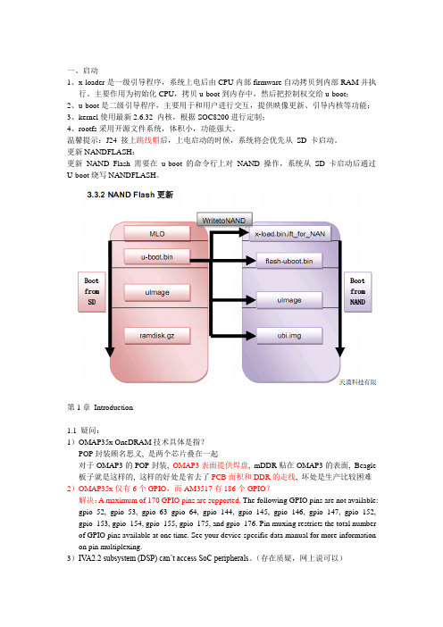
一、启动1、x-loader是一级引导程序,系统上电后由CPU内部firmware自动拷贝到内部RAM并执行。
主要作用为初始化CPU,拷贝u-boot到内存中,然后把控制权交给u-boot;2、u-boot是二级引导程序,主要用于和用户进行交互,提供映像更新、引导内核等功能;3、kernel使用最新2.6.32 内核,根据SOC8200进行定制;4、rootfs采用开源文件系统,体积小,功能强大。
温馨提示:J24 接上跳线帽后,上电启动的时候,系统将会优先从SD 卡启动。
更新NANDFLASH:更新NAND Flash 需要在u-boot 的命令行上对NAND操作,系统从SD卡启动后通过U-boot烧写NANDFLASH。
第1章Introduction1.1 疑问:1)OMAP35x OneDRAM技术具体是指?POP封装顾名思义, 是两个芯片叠在一起对于OMAP3的POP封装, OMAP3表面提供焊盘, mDDR贴在OMAP3的表面, Beagle 板子就是这样的, 这样的好处是省去了PCB面积和DDR的走线, 坏处是生产比较困难2)OMAP35x仅有6个GPIO,而AM3517有186个GPIO?解决:A maximum of 170 GPIO pins are supported. The following GPIO pins are not available: gpio_52, gpio_53, gpio_63 gpio_64, gpio_144, gpio_145, gpio_146, gpio_147, gpio_152, gpio_153, gpio_154, gpio_155, gpio_175, and gpio_176. Pin muxing restricts the total number of GPIO pins available at one time. See your device-specific data manual for more information on pin multiplexing.3)IV A2.2 subsystem (DSP) can’t access SoC peripherals。
omega PHB-357 pH 电容器说明书

PHB-357, $995, shown smaller than actual size.
pH electrode and temperature probe included.
For a complete selection of compatible laboratory pH electrodes, see page C-13 of the GREEN BOOK® section of this handbook.
AVAILABLE FOR FAST DELIVERY!
To Order (Specify Model Number)
Model No.
Price
Description
PHB-357
$995
Micro processor-based benchtop pH meter
PHE-4201
53
Replacement general purpose pH electrode
Temperature Probe Connection: 3 pole, 3.5 mm diameter jack
Reference Electrode Connection: 4 mm diameter
Meter Dimensions: 211 L x 150 W x 89 mm H (8.3 x 5.9 x 3.5") Meter Weight (Including Batteries): 590 g (1.3 lb)
ORE-1411
91
Double junction ORP probe
MN1604
3
9V replacement battery
ES-2139
TI OMAP平台roadmap

First broad sampling of ARM® Cortex™-A8 core provides a 4x improvement over ARM9 and achieves laptop-like performance at handheld power levels
Samples Available Today
L3/L4 Interconnect Peripherals
Connectivity
USB 2.0 HS OTG Controller USB 2.0 Host Controller SDRC GPMC
System
Security Acc (HS only) Timers GP x12 WDT x3
Features
Core
Cortex A-8 DSP based TMS320C64x+ DSP and video accelerators* 600 MHz / 430 MHz @ 1.35V, 550 MHz / 400 MHz @ 1.27V 500 MHz / 360 MHz @ 1.2V NEON™ SIMD Coprocessor 2D/3D Graphics Engine Up to 5M polygons per second
OMAP™
OMAP3503
Begin application development with extensible OMAP35x Evaluation Module
Order EVM Today
3
OMAP™ 35x Scalable Generation of Single-Chip Devices for Complete Portfolio
- 1、下载文档前请自行甄别文档内容的完整性,平台不提供额外的编辑、内容补充、找答案等附加服务。
- 2、"仅部分预览"的文档,不可在线预览部分如存在完整性等问题,可反馈申请退款(可完整预览的文档不适用该条件!)。
- 3、如文档侵犯您的权益,请联系客服反馈,我们会尽快为您处理(人工客服工作时间:9:00-18:30)。
OMAP35x Peripherals OverviewTexas Instruments OMAP™Family of Products Reference GuideLiterature Number:SPRUFN0AJanuary20102SPRUFN0A–January2010Submit Documentation FeedbackCopyright©2010,Texas Instruments IncorporatedPreface (5)1Overview (6)2Memory Management Units(MMU) (7)3System Direct Memory Access(SDMA) (7)4General-Purpose Memory Controller(GPMC) (8)5SDRAM Controller Subsystem(SDRC) (8)6Camera Interface Subsystem(ISP) (8)72D/3D Graphics Accelerator(SGX) (9)8Image Video and Audio Accelerator Subsystem(IVA2.2) (9)9Display Interface Subsystem (10)10Timers (10)11Universal Asynchronous Receiver/Transmitter Module(UART) (11)12Infrared Data Association Module(IrDA) (11)13Consumer Infrared Module(CIR) (11)14Inter-Integrated Circuit Module(I2C) (12)15Multi-channel Serial Port Interface(McSPI) (13)16HDQ/1-Wire Module (13)17Multi-Channel Buffered Serial Port(McBSP) (13)18Multimedia Card/Secure Digital/Secure Digital I/O Card Interface(MMC/SD/SDIO) (14)19High-Speed Universal Serial Bus(USB)OTG Controller and High-Speed USB Host Subsystem (15)20General-Purpose I/O Interface(GPIO) (16)3 SPRUFN0A–January2010Table of Contents Submit Documentation FeedbackCopyright©2010,Texas Instruments IncorporatedList of FiguresList of Tables1Breakdown of OMAP35x Technical Reference Manual (6)4List of Figures SPRUFN0A–January2010Submit Documentation FeedbackCopyright©2010,Texas Instruments IncorporatedPrefaceSPRUFN0A–January2010Read This FirstAbout This ManualThis document provides an overview and briefly describes the peripherals available on the OMAP35xApplications Processor.Related Documentation From Texas InstrumentsThe following documents describe the OMAP35x Applications Processor.The OMAP35x ApplicationsProcessor,related peripherals,and other technical collateral,is available in the OMAP DSP product folder at:/omap.SPRUF98—OMAP35x Technical Reference Manual.Collection of documents providing detailed information on the OMAP3architecture including power,reset,and clock control,interrupts,memory map,and switch fabric interconnect.Detailed information on the microprocessor unit(MPU)subsystem,the image,video,and audio(IVA2.2)subsystem,as well a functional descriptionof the peripherals supported on OMAP35x devices is also included.SPRU732—TMS320C64x/C64x+DSP CPU and Instruction Set Reference Guide.Describes the CPU architecture,pipeline,instruction set,and interrupts for the TMS320C64x and TMS320C64x+digitalsignal processors(DSPs)of the TMS320C6000DSP family.The C64x/C64x+DSP generationcomprises fixed-point devices in the C6000DSP platform.The C64x+DSP is an enhancement ofthe C64x DSP with added functionality and an expanded instruction set.SPRU871—TMS320C64x+DSP Megamodule Reference Guide.Describes the TMS320C64x+digital signal processor(DSP)megamodule.Included is a discussion on the internal direct memory access(IDMA)controller,the interrupt controller,the power-down controller,memory protection,bandwidthmanagement,and the memory and cache.SPRU889—High-Speed DSP Systems Design Reference Guide.Provides recommendations for meeting the many challenges of high-speed DSP system design.These recommendations includeinformation about DSP audio,video,and communications systems for the C5000and C6000DSPplatforms.OMAP is a trademark of Texas Instruments.CORTEX is a trademark of ARM Limited.ARM is a registered trademark of ARM Limited.1-Wire is a registered trademark of Dallas Semiconductor Corp.5 SPRUFN0A–January2010Preface Submit Documentation FeedbackCopyright©2010,Texas Instruments IncorporatedReference GuideSPRUFN0A–January2010OMAP35x Peripherals Overview1OverviewThis document provides an overview and briefly describes the peripherals available on the OMAP35xApplications Processor.The OMAP35x Technical Reference Manual(literature number SPRUF98)describes all peripherals indetail and provides additional information about the OMAP35x applications processors.Table1provides a list of the information contained in the chapters of the OMAP35x Technical Reference Manual.The OMAP35x Technical Reference Manual can be downloaded as a single document or it can bedownloaded on a chapter-by-chapter basis by using the literature numbers given in Table1.The sections that follow provide an overview of the peripherals and other modules available in theOMAP35x applications processors.NOTE:Some features may not be available or supported in your particular device.For moreinformation,see Chapter1,the OMAP35x Family section,and your device-specific datamanual.Table1.Breakdown of OMAP35x Technical Reference Manual6OMAP35x Peripherals Overview SPRUFN0A–January2010Submit Documentation FeedbackCopyright©2010,Texas Instruments Incorporated Memory Management Units(MMU) Table1.Breakdown of OMAP35x Technical Reference Manual(continued)2Memory Management Units(MMU)The OMAP35x device contains three memory management units(MMU):•Microprocessor unit(MPU)MMU.•Camera MMU.•Image Video and Audio accelerator(IVA2.2)MMU.The camera MMU and IVA2.2MMU share the same architecture and are both described in this chapter.The MPU MMU,which implements a different architecture,is covered in the ARM®CORTEX™-A8Technical Reference Manual.NOTE:The MMUn prefix provides information about the register instantiation,where n=1for thecamera MMU,and n=2for the IVA2.2MMU.The MMU instances include the following main features:•N entries fully associative translation look-aside buffer(TLB)with N=8for the camera MMU and N= 32for the IVA2.2MMU.•1interrupt line out to the MPU subsystem.•32-bit virtual addresses,32-bit physical address.•Mapping size:4KB and64KB pages,1MB section,and16MB supersection.•Predefined(static)or table-driven(hardware table walker)software translation strategies.For more information about the memory management units,please refer to the Memory ManagementUnits(MMU)chapter of the OMAP35x Technical Reference Manual.3System Direct Memory Access(SDMA)The System Direct Memory Access(SDMA),also called DMA4,performs high-performance data transfers between memories and peripheral devices without microprocessor unit(MPU)support during transfer.A DMA transfer is programmed through a logical DMA channel,which allows the transfer to be optimallytailored to the requirements of the application.The DMA controller includes the following main features:•Data transfer support in either direction between:–Memory and memory–Memory and peripheral device•32logical DMA channels supporting:–Multiple concurrent transfers–Independent transfer profile for each channel–8-bit,16-bit,or32-bit data element transfer size–Software-triggered or hardware-synchronized transfers–Flexible source and destination address generation–Burst read and write–Chained multiple-channel transfers7 SPRUFN0A–January2010OMAP35x Peripherals Overview Submit Documentation FeedbackCopyright©2010,Texas Instruments IncorporatedGeneral-Purpose Memory Controller(GPMC) –Endianism conversion–Per-channel secure transaction attribute(not available on GP device)•First-come,first-serve DMA scheduling with fixed priority•Up to96DMA requests•Constant fill•Transparent copy•Four programmable interrupt request output lines•Software or hardware enabling•FIFO depth:256x32-bits•Data buffering•FIFO budget allocation•Power-management support•Auto-idle power-saving support•Implementation of retention flip-flops(RFFs)to support dynamic power saving(DPS)between system power modes without MPU involvement•Initiators for secure transactions on the L3and L4interconnect(not available on GP device)The SDMA module has two ports—one read and one write—and provides multiple logical channelsupport.A dynamically allocated FIFO queue memory pool provides buffering between the read and write ports.For more information about the system DMA,please refer to the System Direct Memory Access(SDMA) chapter of the OMAP35x Technical Reference Manual.4General-Purpose Memory Controller(GPMC)The general-purpose memory controller(GPMC)is dedicated to interfacing external memory devices:•Asynchronous SRAM-like memories and application-specific integrated circuit(ASIC)devices•Asynchronous,synchronous,and page mode(only available in non-muxed mode)burst NOR flash devices•NAND flash•Pseudo-SRAM devicesFor more information about the GPMC,please refer to the Memory Subsystem chapter of the OMAP35x Technical Reference Manual.5SDRAM Controller Subsystem(SDRC)The SDRC subsystem module provides connectivity between the OMAP Applications Processor andexternal discrete or POP-ed low-power double-data-rate SDRAM(LPDDR).The SDRC subsystem provides a high-performance interface to a variety of fast memory devices.Itcomprises two submodules:•The SDRAM Memory Scheduler(SMS),consisting of scheduler,security firewall,and virtual rotated frame-buffer(VRFB)modules.•The SDRAM Controller.For more information about the SDRC,please refer to the Memory Subsystem chapter of the OMAP35x Technical Reference Manual.6Camera Interface Subsystem(ISP)The camera ISP is a key component for imaging and video applications such as video preview,videorecord,and still-image capture with or without digital zooming.The camera ISP provides the system interface and the processing capability to connect RAWimage-sensor modules to the OMAP35x Applications Processor.The camera ISP can support the following features:8OMAP35x Peripherals Overview SPRUFN0A–January2010Submit Documentation FeedbackCopyright©2010,Texas Instruments Incorporated2D/3D Graphics Accelerator(SGX)•Image sensor.•Parallel interface:The parallel interface supports two modes.•Video processing:The video-processing hardware removes the need for expensive camera modules to perform processing functions.The video-processing hardware contains a real-time image-pipeline andresizer.•Statistic collection modules(SCM):The host CPU uses statistics to adjust various parameters for processing image data.The SCM provides statistics in real-time.•Central-resource shared buffer logic(SBL):Buffers and schedules memory accesses requested by camera ISP modules.•Circular buffer:Prevents storage of full image frames in memory when data must be postprocessed and/or preprocessed by software.•Memory management unit(MMU):Manages virtual-to-physical address translation for external addresses and solves the memory-fragmentation issue.Enables the camera driver to dynamicallyallocate and deallocate memory;the MMU handles memory fragmentation.•Clock generator:Generates two independent clocks that can be used by two external image sensors.•Secure mode:Used to store sensitive captured images.•Timing control.•Open core protocol(OCP)compliant.For more information about the camera ISP,please refer to the Camera Interface Subsystem(ISP)chapter of the OMAP35x Technical Reference Manual.72D/3D Graphics Accelerator(SGX)The2D/3D graphics accelerator subsystem accelerates2-dimensional(2D)and3-dimensional(3D)graphics applications.The SGX subsystem is based on the SGX core from Imagination Technologies.SGX is a new generation of programmable PowerVR graphics and video IP cores.The PowerVR SGX architecture is scalable and can target all market segments from mainstream mobile devices to high-end desktop graphics.Targeted applications include feature phone,PDA,and hand-held games.The SGX graphics accelerator efficiently processes a number of various multimedia data typesconcurrently:•Pixel data•Vertex data•Video data•General-purpose processingThis is achieved using a multithreaded architecture using two levels of scheduling and data partitioning enabling zero overhead task switching.For more information about the2D/3D graphics accelerators,please refer to the2D/3D GraphicsAccelerator(SGX)chapter of the OMAP35x Technical Reference Manual.8Image Video and Audio Accelerator Subsystem(IVA2.2)The image video and audio accelerator(IVA2.2)is based on the TMS320DMC64X+VLIW digital signal processor(DSP)core.The internal architecture is an assembly of the following components:•High-performance TI DSP(TMS320DMC64X+)integrated in a megacell,including local L1/L2cache and memory controllers•L1RAM and L2RAM and ROM•Video hardware accelerator•Dedicated enhanced data memory access(EDMA)engine to download/upload data from/to memories and peripherals external to the sub-chip•Dedicated memory management unit(MMU)for accessing level3(L3)interconnect address space •Local interconnect network9 SPRUFN0A–January2010OMAP35x Peripherals Overview Submit Documentation FeedbackCopyright©2010,Texas Instruments IncorporatedDisplay Interface Subsystem •Dedicated modules SYSC and WUGEN in charge of power management,clock generation,and connection to the power,reset,and clock manager(PRCM)moduleFor more information about the IVA2.2subsystem,please refer to the Image Video and Audio Accelerator Subsystem(IVA2.2)chapter of the OMAP35x Technical Reference Manual.9Display Interface SubsystemThe display interface subsystem provides the logic to display a video frame from the memory frame buffer (either SDRAM or SRAM)on a liquid-crystal display(LCD)panel or a TV set.The display subsystemintegrates the following elements:•Display controller(DISPC)module•Remote frame buffer interface(RFBI)module•NTSC/PAL video encoderFor more information about the display interface subsystem,please refer to the Display InterfaceSubsystem chapter of the OMAP35x Technical Reference Manual.10TimersThe device has12GP timers:GPTIMER1through GPTIMER12.Each timer can be clocked from either the system clock(12,13,16.8,19.2,26,or38.4MHz)or the32-kHz clock.The selection of the clock source is made at the power,reset,clock management(PRCM) module level.GPTIMER1has its GPT1_EVENT_CAPTURE pin tied to the32-kHz clock and can be used to gauge the system clock input;it detects its frequency among12,13,16.38,19.2,26,or38.4MHz.Each timer can provide an interrupt to the microprocessor unit(MPU)subsystem.In addition,GPTIMER5 through GPTIMER8also have interrupts connected to the IVA2.2subsystem.GPTIMER1,GPTIMER2,and GPTIMER10include specific functions to generate accurate tick interrupts to the operating system.GPTIMER8through GPTIMER11are connected to external pins by their PWMoutput or their event capture input pin(for external timer triggering).The following are the main features of the GP timers controllers:•L4slave interface support:–32-bit data bus width–32-/16-bit access supported–8-bit access not supported–10-bit address bus width–Burst mode not supported–Write nonposted transaction mode supported•Interrupts generated on overflow,compare,and capture•Free-running32-bit upward counter•Compare and capture modes•Autoreload mode•Start/stop mode•Programmable divider clock source(2n with n=[0:8])•Dedicated input trigger for capture mode and dedicated output trigger/PWM signal•Dedicated output signal for general-purpose using GPTi_GPOCFG signal•On-the-fly read/write register(while counting)•1-ms tick with32,768Hz functional clock generated(only GPTIMER1,GPTIMER2,and GPTIMER10) For more information about the timers,please refer to the Timers chapter of the OMAP35x TechnicalReference Manual.10OMAP35x Peripherals Overview SPRUFN0A–January2010Submit Documentation FeedbackCopyright©2010,Texas Instruments Incorporated Universal Asynchronous Receiver/Transmitter Module(UART) 11Universal Asynchronous Receiver/Transmitter Module(UART)The OMAP35x Applications Processor contains three universal asynchronous receiver/transmitter(UART) devices controlled by the microprocessor unit(MPU).•Two UART-only modules,UART1and UART2,are pinned out for use as UART devices only.UART1and UART2must be programmed by setting the UARTi.MDR1_REG[2:0]MODE_SELECT field to one of the three UART operating modes.•UART3,which adds infrared communication support,is pinned out for use as a UART,infrared data association(IrDA),or consumer infrared(CIR)device,and can be programmed to any availableoperating mode.The UARTs(UART1,UART2,and UART3when in UART mode)include the following key features:•16C750compatibility•64-byte FIFO for receiver and64-byte FIFO for transmitter•Programmable interrupt trigger levels for FIFOs•Baud generation based on programmable divisors N(N=1…16,384)operating from a fixed functional clock of48MHzOversampling is programmed by software as16or13;thus,the baud rate computation is either:•Baud rate=(functional clock/16)/N•Baud rate=(functional clock/13)/NThis software programming mode enables higher baud rates with the same error amount without changing the clock source:•Break character detection and generation•Configurable data format–Data bit:5,6,7,or8bits–Parity bit:Even,odd,none–Stop-bit:1,1.5,2bit(s)•Flow control:Hardware(RTS/CTS)or software(XON/XOFF)The UART clocks are connected to produce a baud rate of up to3.6M bits/s.For more information about the UARTs,please refer to the Universal Asynchronous Receiver/Transmitter Module(UART)chapter of the OMAP35x Technical Reference Manual.12Infrared Data Association Module(IrDA)The IrDA(UART3only)includes the following key features:•Support of IrDA1.4slow infrared(SIR),medium infrared(MIR),and fast infrared(FIR)communications –Frame formatting:Addition of variable beginning-of-frame(xBOF)characters and end-of-frame (EOF)characters–Uplink/downlink cyclic redundancy check(CRC)generation/detection–Asynchronous transparency(automatic insertion of break character)–Eight-entry status FIFO(with selectable trigger levels)to monitor frame length and frame errors–Framing error,CRC error,illegal symbol(FIR),and abort pattern(SIR,MIR)detection For more information about the IrDA,please refer to the Infrared Data Association Module(IrDA)chapter of the OMAP35x Technical Reference Manual.13Consumer Infrared Module(CIR)The CIR mode uses a variable pulse-width modulation(PWM)technique(based on multiples of aprogrammable t period)to encompass the various formats of infrared encoding for remote-controlapplications.The CIR logic transmits and receives data packets based on a user-definable frame structure and packet content.The CIR(UART3only)includes the following key features to provide CIR support for remote controlapplications:11 SPRUFN0A–January2010OMAP35x Peripherals Overview Submit Documentation FeedbackCopyright©2010,Texas Instruments IncorporatedInter-Integrated Circuit Module(I2C)•Transmit and receive•Free data format(supports any remote-control private standards)•Selectable bit rate•Configurable carrier frequency•1/2,5/12,1/3,or1/4carrier duty cycleFor more information about the CIR,please refer to the Consumer Infrared Module(CIR)chapter of the OMAP35x Technical Reference Manual.14Inter-Integrated Circuit Module(I2C)The OMAP35x Applications Processor contains three multimaster high-speed(HS)inter-integrated circuit (I2C)controllers(I2Ci modules,where I=1,2,3),each of which provides an interface between a localhost(LH),such as the MPU subsystem,and any I2C-bus-compatible device that connects through the I2C serial bus.External components attached to the I2C bus can serially transmit/receive up to8bits of data to/from the LH device through the2-wire I2C interface.Each multimaster HS I2C controller can be configured to act like a slave or master I2C-compatible device.Moreover,each multimaster HS I2C controller can be configured in serial camera control bus(SCCB)mode(the SCCB is a serial bus developed by Omnivision Technologies,Inc.)to act as a master on a2-wire SCCB bus.Only multimaster HS I2C controllers I2C2and I2C3can be configured in SCCB mode to act as a master device on a3-wire SCCB bus.The device contains an additional master transmitter HS I2C interface(I2C4)in the PRCM module toperform dynamic voltage control and power sequencing.Texas Instruments Inc.provides a global solution with the device connected to power chips(TPS65950device).For details about the TPS65950device, contact your TI representative.The three multimaster HS I2C controllers have the following features:•Compliance with Philips I2C specification version2.1•Support for standard mode(up to100K bits/s)and fast mode(up to400K bits/s)•Support for HS mode for transfer up to3.4M bits/s•Support for3-wire/2-wire SCCB master mode for I2C2and I2C3modules,2-wire SCCB master mode for I2C1module,up to100K bits/s•7-bit and10-bit device addressing modes•General call•Start/restart/stop•Multimaster transmitter/slave receiver mode•Multimaster receiver/slave transmitter mode•Combined master transmit/receive and receive/transmit mode•Built-in FIFO for buffered read or write–8bytes for I2C1and I2C2–64bytes for I2C3•Module enable/disable capability•Programmable clock generation•8-bit-wide data access•Low-power consumption design•Two DMA channels•Wide interrupt capabilityThe master transmitter HS I2C controller I2C4has the following features:•Support of HS and fast modes•7-bit addressing mode only•Master transmitter mode only•Start/restart/stop12OMAP35x Peripherals Overview SPRUFN0A–January2010Submit Documentation FeedbackCopyright©2010,Texas Instruments Incorporated Multi-channel Serial Port Interface(McSPI) For more information about the I2C,please refer to the Inter-Integrated Circuit Module(I2C)chapter of the OMAP35x Technical Reference Manual.15Multi-channel Serial Port Interface(McSPI)The multichannel serial port interface(McSPI)is a master/slave synchronous serial bus.There are four separate McSPI modules(SPI1,SPI2,SPI3,and SPI4)in the device.The McSPI modules differ asfollows:SPI1supports up to four peripherals,SPI2and SPI3support up to two peripherals,and SPI4supports only one peripheral.The McSPI instances include the following main features:•Serial clock with programmable frequency,polarity,and phase for each channel•Wide selection of SPI word lengths ranging from4bits to32bits•Up to four master channels or single channel in slave mode•Master multichannel mode:–Full duplex/half duplex–Transmit-only/receive-only/transmit-and-receive modes–Flexible I/O port controls per channel–Two direct memory access(DMA)requests(read/write)per channel•Single interrupt line for multiple interrupt source events•Power management through wake-up capabilities•Enable the addition of a programmable start-bit for SPI transfer per channel(start-bit mode)•Support start-bit write command•Support start-bit pause and break sequence•64bytes built-in FIFO available for a single channelFor more information about the McSPI,please refer to the Multi-channel Serial Port Interface(McSPI)chapter of the OMAP35x Technical Reference Manual.16HDQ/1-Wire ModuleThe HDQ/1-Wire module implements the hardware protocol of the master functions of the BenchmarkHDQ and the Dallas Semiconductor1-Wire®protocols.These protocols use a single wire forcommunication between the master(HDQ/1-Wire controller)and the slave(HDQ/1-Wire externalcompliant device).The HDQ and1-Wire module has a generic L4interface and is intended to be used in an interrupt-driven fashion.The one-pin interface is implemented as an open-drain output at the device level.The HDQ operates from a fixed12-MHz functional clock provided by the PRCM module.Only the MPU subsystem uses the HDQ/1-Wire module.The main features of the HDQ/1-Wire module support the following:•Benchmark HDQ protocol•Dallas Semiconductor1-Wire®protocol•Power-down modeFor more information about the HDQ/1-wire module,please refer to the HDQ/1-Wire Module chapter of the OMAP35x Technical Reference Manual.17Multi-Channel Buffered Serial Port(McBSP)The multi-channel buffered serial port(McBSP)provides a full-duplex direct serial interface between the device and other devices in a system such as other application chips(digital base band),audio and voice codec(TPS65950device),etc.Because of its high level of versatility,it can accommodate a wide range of peripherals and clocked frame oriented protocols.The OMAP35x device provides five instances of the McBSP modules,called McBSP1,McBSP2,McBSP3, McBSP4,and McBSP5.13 SPRUFN0A–January2010OMAP35x Peripherals Overview Submit Documentation FeedbackCopyright©2010,Texas Instruments IncorporatedMultimedia Card/Secure Digital/Secure Digital I/O Card Interface(MMC/SD/SDIO)The main features of the McBSP modules are:•L4interconnect slave interface supports:–32-bit data bus width–32-bit access supported–16-/8-bit access not supported–10-bit address bus width–Burst mode not supported–Write nonposted transaction mode supported•128x32-bit words(512bytes)for each buffer for transmit/receive operations(McBSP1,3,4,5)•5K bytes(1024x32bits for audio buffer+256×32bits for buffer)for each buffer for transmit/receive audio operations(McBSP2only)•Interrupts configurable in legacy mode(2requests)or PRCM compliant(1request)•Transmit and receive DMA requests triggered with programmable FIFO thresholds•SIDETONE core support:Audio loopback capability(McBSP2and3only)•Multidrop support•Serial interface description–6pin configuration(McBSP1only)–4pin configuration(McBSP2,3,4,5)–Full-duplex communication–Multichannel selection modes•Support to enable or block transfers in each of the channels•128channels for transmission and for reception–Direct interface to industry-standard codecs,analog interface chips(AICs),and other serially connected A/D and D/A devices:•Inter-IC sound(I2S)compliant devices•Pulse code modulation(PCM)devices•Time division multiplexed(TDM)bus devices–A wide selection of data sizes:8,12,16,20,24,and32bits–Bit reordering(send/receive least significant bit[LSB])•Clock and frame-synchronization generation support:–Independent clocking and framing for reception and for transmission up to48MHz–Support for external generation of clock signals and frame-synchronization(frame-sync)signals–A programmable sample rate generator for internal generation and control of clock signals and frame-sync signals–Programmable polarity for frame-sync pulses and for clock signalsFor more information about the McBSP,please refer to the Multi-Channel Buffered Serial Port(McBSP) chapter of the OMAP35x Technical Reference Manual.18Multimedia Card/Secure Digital/Secure Digital I/O Card Interface(MMC/SD/SDIO)The OMAP35x Applications Processor contains three multimedia card high-speed/secure data/securedigital I/O(MMC/SD/SDIO)host controller which provides an interface between a local host(LH)such asa microprocessor unit(MPU)or digital signal processor(DSP)and either MMC,SD memory cards,orSDIO cards and handles MMC/SD/SDIO transactions with minimal LH intervention.The application interface manages transaction semantics.The MMC/SD/SDIO host controller deals with MMC/SD/SDIO protocol at transmission level,data packing,adding cyclic redundancy checks(CRC),start/end bit,and checking for syntactical correctness.The application interface can send every MMC/SD/SDIO command and either poll for the status of the adapter or wait for an interrupt request,which is sent back in case of exceptions or to warn of end ofoperation.14OMAP35x Peripherals Overview SPRUFN0A–January2010Submit Documentation FeedbackCopyright©2010,Texas Instruments Incorporated。