IC datasheet pdf-TPIC44L01,pdf (4-Channel Serial And Parallel Low-Side Pre-FET Driver )
IC datasheet pdf-MX25L1005C pdf,datasheet

MX25L1005C DATASHEET1M-BIT [x 1] CMOS SERIAL FLASH FEATURESGENERAL• Serial Peripheral Interface compatible -- Mode 0 and Mode 3• 1,048,576 x 1 bit structure• 32 Equal Sectors with 4K byte each- Any Sector can be erased individually• 2 Equal Blocks with 64K byte each- Any Block can be erased individually• Single Power Supply Operation- 2.7 to 3.6 volt for read, erase, and program operations• Latch-up protected to 100mA from -1V to Vcc +1VPERFORMANCE• High Performance- Fast access time: 85MHz serial clock- Fast program time: 1.4ms(typ.) and 5ms(max.)/page (256-byte per page)- Fast erase time: 60ms(typ.)/sector (4K-byte per sector) ; 1s(typ.) and 2s(max.)/block (64K-byte per block)• Low Power Consumption- Low active read current: 12mA(max.) at 85MHz and 4mA(max.) at 33MHz- Low active programming current: 15mA (max.)- Low active erase current: 15mA (max.)- Low standby current: 10uA (max.)• Minimum 100,000 erase/program cycles• 20 years data retentionSOFTWARE FEATURES• I nput Data Format- 1-byte Command code• Block Lock protection- The BP0~BP1 status bit defines the size of the area to be software protected against Program and Erase instructions.• A uto Erase and Auto Program Algorithm- Automatically erases and verifies data at selected sector- Automatically programs and verifies data at selected page by an internal algorithm that automatically times the program pulse widths (Any page to be programed should have page in the erased state first)• Status Register Feature• Electronic Identification- JEDEC 2-byte Device ID- RES command, 1-byte Device IDHARDWARE FEATURES• S CLK Input- Serial clock input• SI Input- Serial Data Input• SO Output- Serial Data Output• WP# pin- Hardware write protection• HOLD# pin- pause the chip without diselecting the chip• PACKAGE- 8-pin SOP (150mil)- 8-land USON (2x3x0.6mm)- All Pb-free devices are RoHS CompliantGENERAL DESCRIPTIONMX25L1005C is a CMOS 1,048,576 bit serial Flash memory, which is configured as 131,072 x 8 internally.The MX25L1005C feature a serial peripheral interface and software protocol allowing operation on a simple 3-wire bus. The three bus signals are a clock input (SCLK), a serial data input (SI), and a serial data output (SO). Serial access to the device is enabled by CS# input.The MX25L1005C provide sequential read operation on whole chip.After program/erase command is issued, auto program/ erase algorithms which program/ erase and verify the speci-fied page or sector/block locations will be executed. Program command is executed on page (256 bytes) basis, and erase command is executes on chip or sector(4K-bytes) or block(64K-bytes).To provide user with ease of interface, a status register is included to indicate the status of the chip. The status read command can be issued to detect completion status of a program or erase operation via WIP bit.When the device is not in operation and CS# is high, it is put in standby mode and draws less than 10uA DC cur-rent.The MX25L1005C utilize Macronix's proprietary memory cell, which reliably stores memory contents even after 100,000 program and erase cycles.PIN CONFIGURATIONSPIN DESCRIPTION8-PIN SOP (150mil)8-LAND USON (2x3mm)CS#SO WP#GNDVCC HOLD#SCLK SICS#SO WP#GNDVCC HOLD#SCLK SISYMBOL DESCRIPTION CS#Chip SelectSI Serial Data Input SO Serial Data Output SCLK Clock InputHOLD#Hold, to pause the device without deselecting the device VCC + 3.3V Power Supply GNDGroundDATA PROTECTIONThe MX25L1005C is designed to offer protection against accidental erasure or programming caused by spurious system level signals that may exist during power transition. During power up the device automatically resets the state machine in the standby mode. In addition, with its control register architecture, alteration of the memory con-tents only occurs after successful completion of specific command sequences. The device also incorporates sev-eral features to prevent inadvertent write cycles resulting from VCC power-up and power-down transition or system noise.• Valid command length checking: The command length will be checked whether it is at byte base and completed on byte boundary.• Write Enable (WREN) command: WREN command is required to set the Write Enable Latch bit (WEL) before other command to change data. The WEL bit will return to reset stage under following situation:- Power-up- Write Disable (WRDI) command completion- Write Status Register (WRSR) command completion- Page Program (PP) command completion- Sector Erase (SE) command completion- Block Erase (BE) command completion- Chip Erase (CE) command completion• Software Protection Mode (SPM): by using BP0-BP1 bits to set the part of Flash protected from data change.• Hardware Protection Mode (HPM): by using WP# going low to protect the BP0-BP1 bits and SRWD bit from data change.• Deep Power Down Mode: By entering deep power down mode, the flash device also is under protected from writing all commands except Release from deep power down mode command (RDP) and Read Electronic Sig-nature command (RES).Table 1. Protected Area SizesHOLD FEATUREHOLD# pin signal goes low to hold any serial communications with the device. The HOLD feature will not stop the operation of write status register, programming, or erasing in progress.The operation of HOLD requires Chip Select(CS#) keeping low and starts on falling edge of HOLD# pin signal while Serial Clock (SCLK) signal is being low (if Serial Clock signal is not being low, HOLD operation will not start until Serial Clock signal being low). The HOLD condition ends on the rising edge of HOLD# pin signal while Se-rial Clock(SCLK) signal is being low( if Serial Clock signal is not being low, HOLD operation will not end until Serial Clock being low), see Figure 1.Figure 1. Hold Condition OperationThe Serial Data Output (SO) is high impedance, both Serial Data Input (SI) and Serial Clock (SCLK) are don't care during the HOLD operation. If Chip Select (CS#) drives high during HOLD operation, it will reset the internal logic of the device. To re-start communication with chip, the HOLD# must be at high and CS# must be at low.Status bitProtect level 1Mb BP1 BP00 0 0 (none) None 0 1 1 (1 block) Block 1 1 0 2 (2 blocks) All 113 (All)AllTable 2. COMMAND DEFINITION(1) ADD=00H will output the manufacturer's ID first and ADD=01H will output device ID first.(2) It is not allowed to adopt any other code which is not in the above command definition table.Command (byte)WREN (write enable)WRDI (write disable)RDID (read identification)RDSR (read status register)WRSR (write status register)READ (read data)FAST READ(fast readdata)SE (sectorerase)1st byte 06 (hex)04 (hex)9F (hex)05 (hex)01 (hex)03 (hex)0B (hex)20 (hex)2nd byte AD1 AD1AD13rd byte AD2 AD2AD24th byte AD3 AD3AD35th byte xAction sets the (WEL) write enable latch bit resets the (WEL) write enable latch bit outputs JEDEC ID: 1-byte Manufacturer ID & 2-byte Device IDto read out the values of the status register to write new values of the status registern bytes read out until CS# goes high n bytes read out until CS# goes high to erase the selected sectorCommand(byte)BE (block erase)CE (chip erase)PP (page program)DP (Deep power down)RDP (Releasefrom deeppower down)RES (read electronic ID)REMS (readelectronicmanufacturer &device ID)1st byte D8 (hex)60 or C7 (hex)02 (hex)B9 (hex)AB (hex)AB (hex)90 (hex)2nd byte AD1 AD1 x x 3rd byte AD2 AD2 x x 4th byteAD3 AD3x ADD (1)Actionto erase the selected block to erase whole chip to program the selected pageenters deeppower down moderelease from deep power down mode to read out 1-byte Device ID output the Manufacturer ID & Device IDTable 3. Memory OrganizationBlock Sector Address Range13101F000h01FFFFh ::: 16010000h010FFFh01500F000h00FFFFh ::: 3003000h003FFFh 2002000h002FFFh 1001000h001FFFh 0000000h000FFFhDEVICE OPERATION1. Before a command is issued, status register should be checked to ensure device is ready for the intended op-eration.2. When incorrect command is inputted to this LSI, this LSI becomes standby mode and keeps the standby mode until next CS# falling edge. In standby mode, SO pin of this LSI should be High-Z.3. When correct command is inputted to this LSI, this LSI becomes active mode and keeps the active mode until next CS# rising edge.4. Input data is latched on the rising edge of Serial Clock(SCLK) and data shifts out on the falling edge of SCLK. The difference of Serial mode 0 and mode 3 is shown as Figure 2.5. For the following instructions: RDID, RDSR, READ, FAST_READ, RES and REMS the shifted-in instruction se-quence is followed by a data-out sequence. After any bit of data being shifted out, the CS# can be high. For the following instructions: WREN, WRDI, WRSR, SE, BE, CE, PP , RDP and DP the CS# must go high exactly at the byte boundary; otherwise, the instruction will be rejected and not executed.6. During the progress of Write Status Register, Program, Erase operation, to access the memory array is neglect-ed and not affect the current operation of Write Status Register, Program, Erase.Figure 2. Serial Modes SupportedNote:CPOL indicates clock polarity of Serial master, CPOL=1 for SCLK high while idle, CPOL=0 for SCLK low while not transmitting. CPHA indicates clock phase. The combination of CPOL bit and CPHA bit decides which Serial mode is supported.SCLKMSBCPHA shift inshift outSI 01CPOL(Serial mode 0)(Serial mode 3)1SO SCLKMSBCOMMAND DESCRIPTION(1) Write Enable (WREN)The Write Enable (WREN) instruction is for setting Write Enable Latch (WEL) bit. For those instructions like PP, SE, BE, CE, and WRSR, which are intended to change the device content, should be set every time after the WREN in-struction setting the WEL bit.The sequence of issuing WREN instruction is: CS# goes low→ sending WREN instruction code→ CS# goes high. (see Figure 11)(2) Write Disable (WRDI)The Write Disable (WRDI) instruction is for resetting Write Enable Latch (WEL) bit.The sequence of issuing WRDI instruction is: CS# goes low→ sending WRDI instruction code→ CS# goes high. (see Figure 12)The WEL bit is reset by following situations:- Power-up- Write Disable (WRDI) instruction completion- Write Status Register (WRSR) instruction completion- Page Program (PP) instruction completion- Sector Erase (SE) instruction completion- Block Erase (BE) instruction completion- Chip Erase (CE) instruction completion(3) Read Identification (RDID)The RDID instruction is for reading the manufacturer ID of 1-byte and followed by Device ID of 2-byte. The MXIC Manufacturer ID is C2(hex), the memory type ID is 20(hex) as the first-byte device ID, and the individual device ID of second-byte ID is as followings: 11(hex) for MX25L1005C.The sequence of issuing RDID instruction is: CS# goes low→ sending RDID instruction code → 24-bits ID data out on SO→ to end RDID operation can use CS# to high at any time during data out. (see Figure. 13)While Program/Erase operation is in progress, it will not decode the RDID instruction, so there's no effect on the cy-cle of program/erase operation which is currently in progress. When CS# goes high, the device is at standby stage.(4) Read Status Register (RDSR)The RDSR instruction is for reading Status Register Bits. The Read Status Register can be read at any time (even in program/erase/write status register condition) and continuously. It is recommended to check the Write in Progress (WIP) bit before sending a new instruction when a program, erase, or write status register operation is in progress. The sequence of issuing RDSR instruction is: CS# goes low→ sending RDSR instruction code→ Status Register data out on SO (see Figure. 14)The definition of the status register bits is as below:WIP bit. The Write in Progress (WIP) bit, a volatile bit, indicates whether the device is busy in program/erase/write status register progress. When WIP bit sets to 1, which means the device is busy in program/erase/write status register progress. When WIP bit sets to 0, which means the device is not in progress of program/erase/write status register cycle.WEL bit. The Write Enable Latch (WEL) bit, a volatile bit, indicates whether the device is set to internal write enable latch. When WEL bit sets to 1, which means the internal write enable latch is set, the device can accept program/erase/write status register instruction. When WEL bit sets to 0, which means no internal write enable latch; the de-vice will not accept program/erase/write status register instruction.BP1, BP0 bits. The Block Protect (BP1, BP0) bits, non-volatile bits, indicate the protected area(as defined in table 1) of the device to against the program/erase instruction without hardware protection mode being set. To write the Block Protect (BP1, BP0) bits requires the Write Status Register (WRSR) instruction to be executed. Those bits define the protected area of the memory to against Page Program (PP), Sector Erase (SE), Block Erase (BE) and Chip Erase(CE) instructions (only if all Block Protect bits set to 0, the CE instruction can be executed)SRWD bit. The Status Register Write Disable (SRWD) bit, non-volatile bit, is operated together with Write Protec-tion (WP#) pin for providing hardware protection mode. The hardware protection mode requires SRWD sets to 1 and WP# pin signal is low stage. In the hardware protection mode, the Write Status Register (WRSR) instruction is no longer accepted for execution and the SRWD bit and Block Protect bits (BP1, BP0) are read only.Note: 1. See the table "Protected Area Sizes".2. The endurance cycles of protect bits are 100,000 cycles; however, the tW time out spec of protect bits isrelaxed as tW = N x 15ms (N is a multiple of 10,000 cycles, ex. N = 2 for 20,000 cycles) after 10,000 cycles on those bits.bit7bit6bit5bit4bit3bit2bit1bit0SRWD (status register write protect)00)BP1 (level of protected block)BP0 (level of protected block)WEL (write enable latch)WIP (write inprogress bit)1=status register write disable(note 1)(note 1)1=write enable 0=not write enable 1=write operation 0=not in write operation(5) Write Status Register (WRSR)The WRSR instruction is for changing the values of Status Register Bits. Before sending WRSR instruction, the Write Enable (WREN) instruction must be decoded and executed to set the Write Enable Latch (WEL) bit in ad-vance. The WRSR instruction can change the value of Block Protect (BP1, BP0) bits to define the protected area of memory (as shown in table 1). The WRSR also can set or reset the Status Register Write Disable (SRWD) bit in accordance with Write Protection (WP#) pin signal. The WRSR instruction cannot be executed once the Hardware Protected Mode (HPM) is entered.The sequence of issuing WRSR instruction is: CS# goes low→ sending WRSR instruction code→ Status Register data on SI→ CS# goes high. (see Figure 15)The WRSR instruction has no effect on b6, b5, b4, b1, b0 of the status register.The CS# must go high exactly at the byte boundary; otherwise, the instruction will be rejected and not executed. The self-timed Write Status Register cycle time (tW) is initiated as soon as Chip Select (CS#) goes high. The Write in Progress (WIP) bit still can be check out during the Write Status Register cycle is in progress. The WIP sets 1 during the tW timing, and sets 0 when Write Status Register Cycle is completed, and the Write Enable Latch (WEL) bit is reset.Table 4. Protection ModesNote:1. As defined by the values in the Block Protect (BP1, BP0) bits of the Status Register, as shown in Table 1.As the above table showing, the summary of the Software Protected Mode (SPM) and Hardware Protected Mode (HPM). Software Protected Mode (SPM):- When SRWD bit=0, no matter WP# is low or high, the WREN instruction may set the WEL bit and can changethe values of SRWD, BP1, BP0. The protected area, which is defined by BP1, BP0, is at software protected mode (SPM).- When SRWD bit=1 and WP# is high, the WREN instruction may set the WEL bit can change the values ofSRWD, BP1, BP0. The protected area, which is defined by BP1, BP0, is at software protected mode (SPM)Note: If SRWD bit=1 but WP# is low, it is impossible to write the Status Register even if the WEL bit has previously been set. It is rejected to write the Status Register and not be executed.ModeStatus register condition WP# and SRWD bit status Memory Software protectionmode(SPM)Status register can be written in (WEL bit is set to "1") andthe SRWD, BP0-BP1bits can be changed WP#=1 and SRWD bit=0, or WP#=0 and SRWD bit=0, or WP#=1 and SRWD=1The protected areacannotbe program or erase.Hardware protectionmode (HPM)The SRWD, BP0-BP1 of status register bits cannot bechangedWP#=0, SRWD bit=1The protected areacannotbe program or erase.Hardware Protected Mode (HPM):- When SRWD bit=1, and then WP# is low (or WP# is low before SRWD bit=1), it enters the hardware protected mode (HPM). The data of the protected area is protected by software protected mode by BP1, BP0 and hard-ware protected mode by the WP# to against data modification.Note: to exit the hardware protected mode requires WP# driving high once the hardware protected mode is entered. If the WP# pin is permanently connected to high, the hardware protected mode can never be entered; only can use software protected mode via BP1, BP0.(6) Read Data Bytes (READ)The read instruction is for reading data out. The address is latched on rising edge of SCLK, and data shifts out on the falling edge of SCLK at a maximum frequency fR. The first address byte can be at any location. The address is automatically increased to the next higher address after each byte data is shifted out, so the whole memory can be read out at a single READ instruction. The address counter rolls over to 0 when the highest address has been reached.The sequence of issuing READ instruction is: CS# goes low→ sending READ instruction code→ 3-byte address on SI→data out on SO→ to end READ operation can use CS# to high at any time during data out. (see Figure. 16) (7) Read Data Bytes at Higher Speed (FAST_READ)The FAST_READ instruction is for quickly reading data out. The address is latched on rising edge of SCLK, and data of each bit shifts out on the falling edge of SCLK at a maximum frequency fC. The first address byte can be at any location. The address is automatically increased to the next higher address after each byte data is shifted out, so the whole memory can be read out at a single FAST_READ instruction. The address counter rolls over to 0 when the highest address has been reached.The sequence of issuing FAST_READ instruction is: CS# goes low→ sending FAST_READ instruction code→3-byte address on SI→1-dummy byte address on SI→data out on SO→ to end FAST_READ operation can use CS# to high at any time during data out. (see Figure. 17)While Program/Erase/Write Status Register cycle is in progress, FAST_READ instruction is rejected without any im-pact on the Program/Erase/Write Status Register current cycle.(8) Sector Erase (SE)The Sector Erase (SE) instruction is for erasing the data of the chosen sector to be "1". A Write Enable (WREN) in-struction must execute to set the Write Enable Latch (WEL) bit before sending the Sector Erase (SE). Any address of the sector (see table 3) is a valid address for Sector Erase (SE) instruction. The CS# must go high exactly at the byte boundary (the latest eighth of address byte been latched-in); otherwise, the instruction will be rejected and not executed.Address bits [Am-A12] (Am is the most significant address) select the sector address.The sequence of issuing SE instruction is: CS# goes low→ sending SE instruction code→ 3-byte address on SI →CS# goes high. (see Figure 19)The self-timed Sector Erase Cycle time (tSE) is initiated as soon as Chip Select (CS#) goes high. The Write in Progress (WIP) bit still can be check out during the Sector Erase cycle is in progress. The WIP sets 1 during the tSE timing, and sets 0 when Sector Erase Cycle is completed, and the Write Enable Latch (WEL) bit is reset. If the page is protected by BP1, BP0 bits, the Sector Erase (SE) instruction will not be executed on the page.(9) Block Erase (BE)The Block Erase (BE) instruction is for erasing the data of the chosen block to be "1". A Write Enable (WREN) in-struction must execute to set the Write Enable Latch (WEL) bit before sending the Block Erase (BE). Any address of the block (see table 3) is a valid address for Block Erase (BE) instruction. The CS# must go high exactly at the byte boundary (the latest eighth of address byte been latched-in); otherwise, the instruction will be rejected and not executed.The sequence of issuing BE instruction is: CS# goes low→ sending BE instruction code→ 3-byte address on SI → CS# goes high. (see Figure 20)The self-timed Block Erase Cycle time (tBE) is initiated as soon as Chip Select (CS#) goes high. The Write in Progress (WIP) bit still can be check out during the Sector Erase cycle is in progress. The WIP sets 1 during the tBE timing, and sets 0 when Sector Erase Cycle is completed, and the Write Enable Latch (WEL) bit is reset. If the page is protected by BP1, BP0 bits, the Block Erase (BE) instruction will not be executed on the page.(10) Chip Erase (CE)The Chip Erase (CE) instruction is for erasing the data of the whole chip to be "1". A Write Enable (WREN) instruc-tion must execute to set the Write Enable Latch (WEL) bit before sending the Chip Erase (CE). Any address of the sector (see table 3) is a valid address for Chip Erase (CE) instruction. The CS# must go high exactly at the byte boundary( the latest eighth of address byte been latched-in); otherwise, the instruction will be rejected and not ex-ecuted.The sequence of issuing CE instruction is: CS# goes low→sending CE instruction code→ CS# goes high. (see Fig-ure 20)The self-timed Chip Erase Cycle time (tCE) is initiated as soon as Chip Select (CS#) goes high. The Write in Progress (WIP) bit still can be check out during the Chip Erase cycle is in progress. The WIP sets 1 during the tCE timing, and sets 0 when Chip Erase Cycle is completed, and the Write Enable Latch (WEL) bit is reset. If the chip is protected by BP1, BP0 bits, the Chip Erase (CE) instruction will not be executed. It will be only executed when BP1, BP0 all set to "0".(11) Page Program (PP)The Page Program (PP) instruction is for programming the memory to be "0". A Write Enable (WREN) instruction must execute to set the Write Enable Latch (WEL) bit before sending the Page Program (PP). If the eight least sig-nificant address bits (A7-A0) are not all 0, all transmitted data which goes beyond the end of the current page are programmed from the start address if the same page (from the address whose 8 least significant address bits (A7-A0) are all 0). The CS# must keep during the whole Page Program cycle. The CS# must go high exactly at the byte boundary( the latest eighth of address byte been latched-in); otherwise, the instruction will be rejected and not executed. If more than 256 bytes are sent to the device, the data of the last 256-byte is programmed at the request page and previous data will be disregarded. If less than 256 bytes are sent to the device, the data is programmed at the request address of the page without effect on other address of the same page.The sequence of issuing PP instruction is: CS# goes low→ sending PP instruction code→ 3-byte address on SI→at least 1-byte on data on SI→CS# goes high. (see Figure 18)The self-timed Page Program Cycle time (tPP) is initiated as soon as Chip Select (CS#) goes high. The Write in Progress (WIP) bit still can be check out during the Page Program cycle is in progress. The WIP sets 1 during the tPP timing, and sets 0 when Page Program Cycle is completed, and the Write Enable Latch (WEL) bit is reset. If the page is protected by BP1, BP0 bits, the Page Program (PP) instruction will not be executed.(12) Deep Power-down (DP)The Deep Power-down (DP) instruction is for setting the device on the minimizing the power consumption (to enter-ing the Deep Power-down mode), the standby current is reduced from ISB1 to ISB2). The Deep Power-down mode requires the Deep Power-down (DP) instruction to enter, during the Deep Power-down mode, the device is not ac-tive and all Write/Program/Erase instruction are ignored. When CS# goes high, it's only in standby mode not deep power-down mode. It's different from Standby mode.The sequence of issuing DP instruction is: CS# goes low→ sending DP instruction code→CS# goes high. (see Fig-ure 22)Once the DP instruction is set, all instruction will be ignored except the Release from Deep Power-down mode (RDP) and Read Electronic Signature (RES) instruction. (RES instruction to allow the ID been read out). When Power-down, the deep power-down mode automatically stops, and when power-up, the device automatically is in standby mode. For RDP instruction the CS# must go high exactly at the byte boundary (the latest eighth bit of instruction code been latched-in); otherwise, the instruction will not executed. As soon as Chip Select (CS#) goes high, a delay of tDP is required before entering the Deep Power-down mode and reducing the current to ISB2.(13) Release from Deep Power-down (RDP), Read Electronic Signature (RES)The Release from Deep Power-down (RDP) instruction is terminated by driving Chip Select (CS#) High. When Chip Select (CS#) is driven High, the device is put in the Stand-by Power mode. If the device was not previously in the Deep Power-down mode, the transition to the Stand-by Power mode is immediate. If the device was previously in the Deep Power-down mode, though, the transition to the Stand-by Power mode is delayed by tRES2, and Chip Select (CS#) must remain High for at least tRES2(max), as specified in Table 6. Once in the Stand-by Power mode, the device waits to be selected, so that it can receive, decode and execute instructions.RES instruction is for reading out the old style of 8-bit Electronic Signature, whose values are shown as table of ID Definitions. This is not the same as RDID instruction. It is not recommended to use for new design. For new deisng, please use RDID instruction. Even in Deep power-down mode, the RDP and RES are also allowed to be executed, only except the device is in progress of program/erase/write cycle; there's no effect on the current program/erase/ write cycle in progress.The sequence is shown as Figure 23,24.The RES instruction is ended by CS# goes high after the ID been read out at least once. The ID outputs repeat-edly if continuously send the additional clock cycles on SCLK while CS# is at low. If the device was not previously in Deep Power-down mode, the device transition to standby mode is immediate. If the device was previously in Deep Power-down mode, there's a delay of tRES2 to transit to standby mode, and CS# must remain to high at least tRES2(max). Once in the standby mode, the device waits to be selected, so it can be receive, decode, and execute instruction.The RDP instruction is for releasing from Deep Power Down Mode.。
拓品微 TP5410 1A 锂电池充电和 5V 1A 升压控制芯片数据手册说明书
南京拓品微电子有限公司NanJing Top Power ASIC Corp.数据手册DATASHEETTP5410(1A锂电池充电和5V/1A升压控制芯片)特点★典型值高达1000mA 的可编程充电电流,最大可达到1.2A;★高达1A 的升压输出电流(Vbat=3.3V),最高输出1.5A(Vbat=3.8v);★自动频率调整(VFM),适应不同升压负载(5V空载待机电流小于10uA),无需按键启动低电池电压(小于2.7V)自动停止升压;·用于单节锂离子电池移动电源专用电路;·升压高效率:88%(Typ),最大92%;·恒定电流/恒定电压操作,并具有可在无过热危险的情况下实现充电速率最大化的热调节功能;·精度达到±1%的4.2V 预设充电电压;·精度达到±2.5%的5V 预设升压精度,5V 电压可通过外接电阻微调;·最高输入可达10V;·2个充电状态指示:开漏输出驱动LED;·C/5充电终止电流;·2.9V以下涓流充C/5;·充电软启动减少浪涌电流;·无需MOSFET 、检测电阻器或隔离二极管;·8引脚ESOP 散热加强型封装。
应用·移动电源·便携设备绝对最大额定值·输入电源电压(V CC ):-0.3V~12V ·PROG :-0.3V~V CC +0.3V ·BAT :0V~7V·LX :-2V~10V ·VOUT :-0.3V~10V ·CHRG :-0.3V~10V ·BAT 短路持续时间:连续·BAT 引脚电流:1200mA·升压最大输出电流1.8A/5V·最大结温:145℃·工作环境温度范围:-40℃~85℃·贮存温度范围:-65℃~125℃·引脚温度(焊接时间10秒):260℃完整的充电循环(1000mAh电池)描述TP5410为一款移动电源专用的单节锂离子电池充电器和恒定5V 升压控制器,充电部分集高精度电压和充电电流调节器、预充、充电状态指示和充电截止等功能于一体,可以输出最大1A 充电电流。
IC datasheet pdf-REF1004,pdf(Micropower Voltage Reference)

The REF1004 is offered in an 8-lead Plastic SOIC package and shipped in anti-static rails or tape and reel.
Typical Operating Circuit
NC 1 NC 2 NC 3 Anode 4
IR = 100µA
10Hz ≤ IR ≤ 10kHz
60
120
µV
LONG TERM STABILITY
IR = 100µA
TA = 25°C ± 0.1°C
20
2 (1) This specification applies over the full operating temperature range of 0°C ≤ TA ≤ 70°C. (2) This specification applies over the full operating temperature range of 40°C ≤ TA ≤ +85°C. (3) Denotes the specifications which apply over the full operating temperature range.
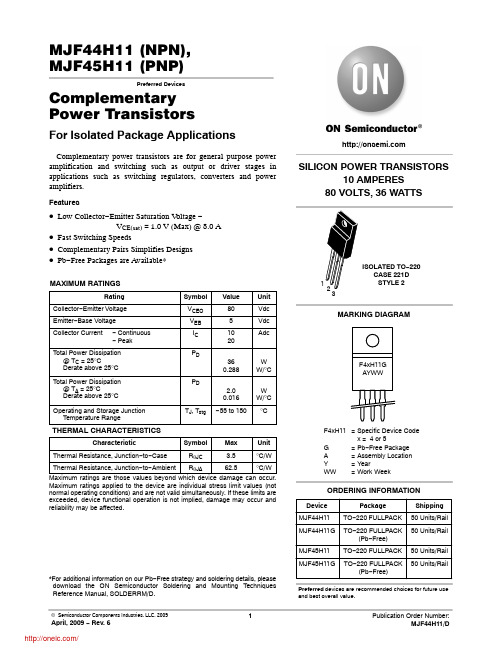
MJD44H11

MJD44H11 Rev. B1
4
Dimensions in Millimeters
TRADEMARKS
The following includes registered and unregistered trademarks and service marks, owned by Fairchild Semiconductor and/or its global subsidiaries, and is not intended to be an exhaustive list of all such trademarks.
LIFE SUPPORT POLICY
FAIRCHILD’S PRODUCTS ARE NOT AUTHORIZED FOR USE AS CRITICAL COMPONENTS IN LIFE SUPPORT DEVICES OR SYSTEMS WITHOUT THE EXPRESS WRITTEN APPROVAL OF FAIRCHILD SEMICONDUCTOR CORPORATION.
As used herein:
1. Life support devices or systems are devices or systems which, (a) are intended for surgical implant into the body or (b) support or sustain life, and (c) whose failure to perform when properly used in accordance with instructions for use provided in the labeling, can be reasonably expected to result in a significant injury of the user.
MJF44H11G;MJF45H11G;MJF44H11;MJF45H11;中文规格书,Datasheet资料
20 30 50 70 100
VCE, COLLECTOR-EMITTER VOLTAGE (VOLTS)
Figure 2. Maximum Rated Forward Bias Safe Operating Area
There are two limitations on the power handling ability of a transistor: average junction temperature and second breakdown. Safe operating area curves indicate IC − VCE limits of the transistor that must be observed for reliable operation; i.e., the transistor must not be subjected to greater dissipation than the curves indicate.
−
−
500
−
−
500
−
−
140
−
−
100
−
Unit Vdc mA mA Vdc Vdc
−
pF MHz
ns ns ns
r(t), TRANSIENT THERMAL RESISTANCE (NORMALIZED)
1.0 0.7 D = 0.5 0.5
0.3 0.2
0.2
0.1 0.1
0.07
0.05
0.05 0.02
MJF44H11 MJF45H11
Symbol VCEO(sus)
ICES IEBO VCE(sat) VBE(sat) hFE
IC datasheet pdf-TL1431,pdf(Precision Programmable Reference)

(5) Maximum power dissipation is a function of TJ(max), θJC, and TC. The maximum allowable power dissipation at any allowable case temperature is PD = (TJ(max) – TC)/θJC. Operating at the absolute maximum TJ of 150°C can affect reliability.
2
PRODUCTION DATA information is current as of publication date. Products conform to specifications per the terms of the Texas Instruments standard warranty. Production processing does not necessarily include testing of all parameters.
FEATURES
1
•2 0.4% Initial Voltage Tolerance • 0.2-Ω Typical Output Impedance • Fast Turnon…500 ns
D PACKAGE (TOP VIEW)
CATHODE 1 ANODE 2 ANODE 3 NC 4
II(ref)
Reference input current range
θJA
44A0111型号双层结构电缆说明书

44A0111-22-444A0111-18-044A0111-26-244 wire44 cable (twisted pair)Specifications/ApprovalsMil-W-81044, Mil-C-27500 (Cables)Def Stan. 61-12 Part 18 Issue 4 - Type 1 pliable (Maintenance Range)Def Stan. 61-12 Part 26 Issue 2 Type 1, 2, 3, 7, 8, 9 & METS 7, 8 & 9VG 95218 Parts 20, 21, 22, 23 and 1000NATO Stock numbers (NSN's) exist for most standard constructions Civil Aviation Authority Accessory Approval E11623Lloyds Register of Shipping NASA Preferred Product List Raychem Specification 44ConductorPrimary Insulation -Radiation Crosslinked,Extruded Polyalkene Jacket -Radiation Crosslinked,Modified PVDF•Dual wall construction•600, 1000 and 2500 voltage rating •Small size, light weight •Low smoke and low corrosive gas generation•Resistant to most chemicals and electrical arc trackingSpec 44Wire and cableSpec 44 wire has a dual wall construction which combines the outstanding physical and electrical characteristics of radiation crosslinked polyalkene with the excellent mechanical and chemical properties of radiation cross-linked polyvinylidene fluoride (PVDF).The result is a wire insulation system that offers a 150°C temperature rating, small size, light weight,solder iron resistance, and resistance to most solvents, fuels and lubricants. Spec 44 wire and cable is highly flame retardant, non-melting, does not cold flow, and though mechanically very tough, is easy to handle and install using conventional tools.Originally developed for aerospace and military requirements in applications of high density and complex circuitry, Spec 44 wire and cable now finds wide use throughout industry, in commercial and military electronics, avionics, on satellites, aircraft, helicopters, ships, trains, and offshore platforms where environmental conditions demand consistently reliable performance. In airframe applications Spec 44 constructions can offer a modern dimensional replacement for PVC/Nylon/Glass braid type wire and cables. Spec 44 wire is offered in a wide range of sizes in stranded conductors, standard materials available being tin or silver-plated copper and high strength copper alloy. Voltage ratings of 600, 1000 and 2500 volts are available as standard. Shielded and jacketed versions include single and multi-conductor constructions and flat braid shields where further size and weight savings are achieved.Spec 44Physical characteristicsTypical propertiesEnvironmental performanceFire hazard performanceSmall sizeSpec 44 equipment wire, 600 volt rated has a 0.19 mm nominal wall thickness compared to 0.25 mm and 0.38 mm for equivalent PTFE and PVC wires in MIL-W-16878, MIL-W-22759 or BS G210.Light weightBecause of the thin wall and low density of the insulation materials considerable weight savings are made over similarly rated PTFE wires, eg:-44A0111-22AWG equipment wire 4.62 grams/metre max22AWG PTFE equipent wire, MIL-W-227595.54 grams/metre max General handlingThe flexibility of Spec 44 and the ease with which it takes a 'set' makes it one of the easiest of the 'high performance' wires to install. Stripping is done with conventional die blade strippers.For details of appropriate tools see separate wire handling guide. The tin-plated conductor usually specified is easily soldered or crimped. The insulation may be hot stamp marked or printed and does not need etching before potting.LengthsSpec 44 is available in long continuous lengths and can be supplied for use on automatic cut and strip wire preparation machines.Temperature rating -65°C to +150°C Voltage rating (thin wall)600 V Voltage rating (thick wall)2500 VTensile strength and elongation of insulation 30 N/mm 2, 230%Notch propagation, 0.05mm notch Pass Solder iron resistance (370°C, 1 minute) Pass Shrinkage, 200°C <1%Low temperature bend -65°C Voltage withstand (thin wall)2500 VInsulation resistance (20°C)1500 M ohms for 1 km Resistance: fuels, oils, solventsPassTemperature ratingSpec 44 wire and cable is rated for continuous operation from -65°C to +150°C and for short periods at temperatures as high as 300°C. Heat ageing tests are routinely performed attemperatures of 200°C (168 h) and 300°C (6 h). In addition Spec 44's insulation will not shrink back under repeated cycling.Mechanical performanceSpec 44 wire provides better cut through resistance than some wires with much thicker walls. 600 volt equipment wire 44A0111 (0.19 mm wall) has 40% greater cut throughresistance than 600 volt PTFE insulated wire (0.25 mm wall).Solder iron/Overload resistanceThe radiation crosslinking of the materials used in Spec 44 makes them non-melting at high temperature. As a result Spec 44 wire isresistant to prolonged contact with solder irons and is resistant to current overloads which would melt most thermoplastic insulations.Chemical resistanceThe irradiated dual wall construction of Spec 44 wire is highly resistant to many acids, alkalis, hydrocarbon solvents,fuels, lubricants, water and many missile fuels and oxidisers.Cold flowRadiation cross-linking of Spec 44 prevents cold flow of the insulation - a recognised problem of some uncrosslinked materials.Voltage ratingsStandard available voltage ratings for Spec 44 wire are 600 volts (0.19 mm wall thickness), 1000 volts (0.28 mm wall) and 2500 volts (0.48 mm wall).Electrical arc track resistanceSpec 44 insulation demonstrates a totalresistance to arc tracking under both wet and dry conditions at aircraft system voltages.Low outgassingFor use in space applications, specialconstructions of Spec 44 wire are available with low outgassing characteristics, for use in an environment of high vacuum and high temperature.FlammabilityBS4066 vertical flammability Pass S424 14751 (Swedish chimney)Pass NFC 32070 (2) (French chimney)Pass IEC 332 part 3 (Cable ladder)PassSmoke/Toxicity IndexSmoke Index, Def Stan 61-12 (18) 6 per metre of wire Toxicity Index, Def Stan 61-12 (18)0.8 per metre of wire Oxygen Index, NES 71430% Oxygen Temperature Index, NES 715>300°CSpec 44Spec 44 wire and cable - nominal sizes, strandings and weights Primary wires/Twisted pair44A011X (600 V)primary wire44A021X (1000 V)primary wire 44A031X (2500 V)primary wire 44A081X (600 V)airframe wire44A012X (600 V)twisted pairSize Stranding (mm)CSA (mm 2)OD (mm)Weight(g/m)OD (mm)Weight (g/m)OD (mm)Weight (g/m)OD (mm)Weight (g/m)OD (mm)Weight (g/m)307/0.100.060.68 1.00 1.37 2.12287/0.130.090.76 1.36 1.49 1.52 2.9026*19/0.100.150.86 1.98 1.02 2.23 1.73 4.102419/0.130.25 1.02 2.97 1.17 3.43 1.44 4.18 1.37 3.73 2.03 6.082219/0.160.40 1.19 4.38 1.37 4.92 1.75 6.12 1.57 5.52 2.388.912019/0.200.60 1.40 6.50 1.577.30 1.988.651.787.912.7913.301819/0.25 1.00 1.659.90 1.8510.90 2.2312.38 2.0311.49 3.3020.211619/0.29 1.25 1.8312.58 2.0613.88 2.4615.37 2.2614.32 3.6525.731419/0.36 2.002.2619.65 2.4920.90 2.9223.13 2.7422.084.5240.151237/0.32 3.00 2.7430.68 2.9831.34 3.3234.32 3.2032.235.4862.631037/0.40 5.00 3.2846.28 3.7350.4 4.0954.02 3.9451.808133/0.295.2387.65.5696.20 5.4492.94*For 44A0211-26 the stranding is 7/0.16mmScreened and jacketed cable44A111X (600 V)1 conductor44A121X (6000 V)1 conductor44A181X (600 V)1 conductor44A112X (600 V)2 conductorsSize Stranding (mm)OD (mm)Weight (g/m)OD (mm)Weight (g/m)OD(mm)Weight (g/m)OD (mm)Weight (g/m)307/0.10 2.238.20287/0.13 1.60 5.33 2.389.402619/0.10 1.57 5.82 1.73 6.51 2.5912.052419/0.13 1.838.20 1.989.18 2.2611.69 2.9916.122219/0.16 2.0010.30 2.2412.35 2.5715.39 3.3521.502019/0.20 2.2614.02 2.5417.40 2.7719.09 3.7627.971819/0.25 2.6219.70 2.8222.61 3.0223.98 4.3238.241619/0.29 2.7923.40 3.0226.63 3.2527.97 4.6744.931419/0.36 3.2232.50 3.4536.15 3.7338.48 5.5364.281237/0.32 3.7045.67 4.1449.55 4.1952.106.5091.51Size 10 to 4 also available in some constructions depending on conductor type and construction required.Spec 44 wire and cable (Def Stan 61-12 Part 18 Issue 4 Type 1) (Maintenance)Limited fire hazard equipment wire (pliable)Cable electrical - Type 1SBM screened and jacketedConductor size Stranding (mm)Diameter over insulation (mm)Weight (gm/m)Raychem part number Diameter over screen (mm)Diameterover jacket (mm)Weight (gm/m)Raychempart number 307/0.100.68 1.0044M9976-30-†287/0.120.73 1.4044M9976-28-†2619/0.100.88 2.0044M9976-26-† 1.33 1.807.544M9995-26-†-†2419/0.120.98 3.0044M9976-24-† 1.43 1.909.244M9995-24-†-†2219/0.15 1.13 4.4044M9976-22-† 1.58 2.0511.144M9995-22-†-†2019/0.20 1.40 6.5544M9976-20-† 1.83 2.3014.644M9995-20-†-†1819/0.25 1.659.9044M9976-18-† 2.08 2.5519.344M9995-18-†-†1619/0.30 1.9014.1544M9976-16-† 2.48 2.9524.944M9995-16-†-†1437/0.25 2.2518.6244M9976-14-† 2.65 3.1330.944M9995-14-†-†1237/0.30 2.6025.7044M9976-12-† 3.00 3.4843.444M9995-12-†-†The cable jackets on type 1SBM are specified black to Def. Stan. 61-12 pt 31, other colours are available.†Colour code suffix - see part numbering system. Single and multicore screened and jacketed cables are available using Type1 components.Spec 44All of the above information, including illustrations, is believed to be reliable. Users, however, should independently evaluate the suitability of each product for their application. Tyco Electronics makes no warranties as to the accuracy or completeness of the information and disclaims any liability regarding its use. Tyco Electronics only obligations are those in the Standard Terms and Conditions of Sale for this product and in no case will Tyco Electronics be liable for any incidental, indirect or consequential damages arising from the sale, resale, use or misuse of the product. Tyco Electronics Specifications are subject to change without notice. In addition Tyco Electronics reserves the right to make changes in materials or processing, without notification to the Buyer, which do not affect compliance with any applicable specification.WC0007.0200Raychem and Spec 44 are trademarks of Tyco Electronics Corporation.Tyco Electronics Corporation 300 Constitution DriveMenlo Park, CA 94025-1164USATel:(800)-926 2425 (US and Canada)Tel: +1 650 361 3860 (All other countries)Tyco Electronics Raychem K.K.3816 Noborito, Tama-ku KawasakiKanagawa 214-8533JapanTel:+81 44 900 5102Raychem Singapore PTE Ltd.26 Ang Mo Kio Industrial Park 2Singapore 569507Tel: +65 4866151Tyco Electronics UK Ltd Faraday Road, Dorcan,Swindon, Wiltshire SN3 5HH Tel:(44)-1793-528171Part numbering system44XXXXX-Size-X/X-XTypical ordering example 3 conductors, brown, yellow with green stripe, blue, white jacket. If 600 volt, round braid, 20 AWG tinned conductor, total part number is 44A1131-20-1/45/6-9.Ordering informationStandard equipment wires (44A0111 12 to 30 AWG) in most common AWGs and colours are kept in stock. In addition, many of the most commonly used single/pair and triple screened cables are also stock items, as are some airframe constructions.Other constructions and custom designed wire and cable are available on request.Jacket colour(in accordance with MIL-STD-681,white preferred)Primary wire insulation colour (in accordance with MIL-STD-681)0=Black 3=Orange 7=Violet 1=Brown 4=Yellow 8=Grey 2=Red 5=Green 9=White 2L=Pink 6=BlueAdditional number after base colour indicates stripe Conductor sizeConductor type 1 - Tin-plated copper 2 - Silver-plated copper4 - Silver-plated high strength copper alloy (SPHSCA)Number of conductors 1 - 9Class of wire1 - 600 V equipment wire2 - 1000 V equipment wire3 - 2500 V equipment wire4 - Space wire 600 V8 - Airframe wire - medium weight Constructions0 - Primary wire & unscreened,unjacketed cables1 - Round braid screened & jacketed †2 - Flat braid screened & jacketed †3 - Round braid, screened, no jacket †4 - Jacketed, no screen5 - Spirally screened & jacket 7 - 9 Special constructions †Screen material same as conductor material except screen for type 4conductor is tinned copper TypeA- AWG conductor M - Metric conductor AM - SpecialCD - Custom Design B - Special/ - Space & specialsD - Defence Standard 61-12 Part 26Basic specification number44A0111-22-444A0111-18-044A0111-26-2。
ICS557-01 Datasheet说明书

PCI-EXPRESS CLOCK SOURCEDescriptionThe ICS557-01 is a clock chip designed for use inPCI-Express Cards as a clock source. It provides a pair of differential outputs at 100 MHz in a small 8-pin SOIC package.Using IDT’s patented Phase-Locked Loop (PLL) techniques, the device takes a 25 MHz crystal input and produces HCSL (Host Clock Signal Level) differential outputs at 100 MHz clock frequency. LVDS signal levels can also be supported via an alternative termination scheme.Features•Supports PCI-Express TM HCSL Outputs0.7 V current mode differential pair •Supports LVDS Output Levels•Packaged in 8-pin SOIC•RoHS 5 (green ) or RoHS 6 (green and lead free) compliant packaging•Operating voltage of 3.3 V•Low power consumption•Input frequency of 25 MHz•Short term jitter 100 ps (peak-to-peak)•Output Enable via pin selection•Industrial temperature range availableBlock DiagramPin Assignment Pin DescriptionsPin NumberPinNamePinTypePin Description1OE Input Output Enable signal(H = outputs are enabled, L = outputs are disabled/tristated).Internal pull-up resistor.2X1Input Crystal or clock input. Connect to a 25 MHz crystal or single ended clock. 3X2XO Crystal Connection. Connect to a parallel mode crystal.Leave floating if clock input.4GND Power Connect to ground.5IREF Output A 475Ω precision resistor connected between this pin and groundestablishes the external reference current.6CLK Output HCSL differential complementary clock output.7CLK Output HCSL differential clock output.8VDD Power Connect to +3.3 V.Applications Information External ComponentsA minimum number of external components are required for proper operation.Decoupling CapacitorsDecoupling capacitors of 0.01 μF should be connected between VDD and the ground plane (pin 4) as close to the VDD pin as possible. Do not share ground vias between components. Route power from power source through the capacitor pad and then into IDT pin.CrystalA 25 MHz fundamental mode parallel resonant crystal with C L = 16 pF should be used. This crystal must have less than 300 ppm of error across temperature in order for theICS557-01 to meet PCI Express specifications.Crystal CapacitorsCrystal capacitors are connected from pins X1 to ground and X2 to ground to optimize the accuracy of the output frequency.C L= Crystal’s load capacitance in pFCrystal Capacitors (pF) = (C L- 8) * 2For example, for a crystal with a 16 pF load cap, each external crystal cap would be 16 pF. (16-8)*2=16.Current Source (Iref) Reference Resistor - R RIf board target trace impedance (Z) is 50Ω, then R R = 475Ω(1%), providing IREF of 2.32 mA. The output current (I OH) is equal to 6*IREF.Output TerminationThe PCI-Express differential clock outputs of the ICS557-01 are open source drivers and require an external series resistor and a resistor to ground. These resistor values and their allowable locations are shown in detail in thePCI-Express Layout Guidelines section.The ICS557-01can also be configured for LVDS compatible voltage levels. See the LVDS Compatible Layout Guidelines sectionGeneral PCB Layout RecommendationsFor optimum device performance and lowest output phase noise, the following guidelines should be observed.1. Each 0.01µF decoupling capacitor should be mounted on the component side of the board as close to the VDD pin as possible.2. No vias should be used between decoupling capacitor and VDD pin.3. The PCB trace to VDD pin should be kept as short as possible, as should the PCB trace to the ground via. Distance of the ferrite bead and bulk decoupling from the device is less critical.4. An optimum layout is one with all components on the same side of the board, minimizing vias through other signal layers (any ferrite beads and bulk decoupling capacitors can be mounted on the back). Other signal traces should be routed away from the ICS557-01.This includes signal traces just underneath the device, or on layers adjacent to the ground plane layer used by the device.PCI-Express Layout GuidelinesFigure 1: PCI-Express Device RoutingTypical PCI-Express (HCSL) WaveformLVDS Compatible Layout GuidelinesFigure: LVDS Device RoutingTypical LVDS WaveformAbsolute Maximum RatingsStresses above the ratings listed below can cause permanent damage to the ICS557-01. These ratings are stress ratings only. Functional operation of the device at these or any other conditions above those indicated in the operational sections of the specifications is not implied. Exposure to absolute maximum rating conditions for extended periods can affect product reliability. Electrical parameters are guaranteed only over the recommended operating temperature range.DC Electrical CharacteristicsUnless stated otherwise, VDD = 3.3 V ±5%, Ambient Temperature -40 to +85°C1 Single edge is monotonic when transitioning through region.2 Inputs with pull-ups/-downs are not included.ItemRatingSupply Voltage, VDD, VDDA 5.5 VAll Inputs and Outputs-0.5 V to VDD+0.5 V Ambient Operating Temperature (commercial)0 to +70°C Ambient Operating Temperature (industrial)-40 to +85°C Storage Temperature -65 to +150°C Junction Temperature 125°C Soldering Temperature 260°CESD Protection (Input)2000 V min. (HBM)ParameterSymbolConditions Min.Typ.Max.UnitsSupply Voltage V 3.135 3.465Input High Voltage 1V IH 2.0VDD +0.3V Input Low Voltage 1V IL VSS-0.30.8V Input Leakage Current 2I IL 0 < Vin < VDD-55μA Operating Supply Current I DD With 50Ω and 2 pF load 55mA I DDOE OE =Low35mA Input Capacitance C IN Input pin capacitance 7pF Output Capacitance C OUT Output pin capacitance 6pF Pin Inductance L PIN 5nH Output Resistance Rout CLK outputs 3.0k ΩPull-up ResistorR PUPOE60k ΩAC Electrical Characteristics - CLK/CLKUnless stated otherwise, VDD=3.3 V ±5%, Ambient Temperature -40 to +85°C1 Test setup is R L =50 ohms with2 pF , R R = 475Ω (1%).2 Measurement taken from a single-ended waveform.3 Measurement taken from a differential waveform.4Measured at the crossing point where instantaneous voltages of both CLKOUT and CLKOUT are equal.5 CLKOUT pins are tri-stated when OE is low asserted. CLKOUT is driven differential when OE is high.Thermal Characteristics (8-pin SOIC)ParameterSymbolConditions Min.Typ.Max.UnitsInput Frequency 25MHz Output Frequency 100MHzOutput High Voltage 1,2V OH 660700850mV Output Low Voltage 1,2V OL-150027mV Crossing Point Voltage 1,2Absolute250350550mV Crossing Point Voltage 1,2,4Variation over all edges140mV Jitter, Cycle-to-Cycle 1,380ps Rise Time 1,2t OR From 0.175 V to 0.525 V 175332700ps Fall Time 1,2t OFFrom 0.525 V to 0.175 V175344700ps Rise/Fall Time Variation 1,2125ps Duty Cycle 1,34555%Output Enable Time 5All outputs 30µs Output Disable Time 5All outputs30µs Stabilization Time t STABLEFrom power-up VDD=3.3 V3.0ms Spread Change Timet SPREAD Settling period after spread change3.0msParameterSymbolConditionsMin.Typ.Max.UnitsThermal Resistance Junction to AmbientθJA Still air150°C/W θJA 1 m/s air flow 140°C/W θJA 3 m/s air flow120°C/W Thermal Resistance Junction to CaseθJC40°C/WMarking Diagram (ICS557M-01LF) Marking Diagram (ICS557MI-01LF)Notes:1. ###### is the lot code.2. YYWW is the last two digits of the year, and the week number that the part was assembled.3. “L ” designates Pb (lead) free packaging.4. “I” denotes industrial temperature.5. Bottom marking: (orgin). Origin = country of origin if not USA.Package Outline and Package Dimensions (8-pin SOIC, 150 Mil. Narrow Body) Package dimensions are kept current with JEDEC Publication No. 95Ordering InformationPart / Order Number Marking Shipping Packaging Package Temperature 557M-01LF See Page 8Tubes8-pin SOIC0 to +70° C557M-01LFT Tape and Reel8-pin SOIC0 to +70° C557MI-01LF Tubes8-pin SOIC-40 to +85° C557MI-01LFT Tape and Reel8-pin SOIC-40 to +85° C"LF" suffix to the part number are the Pb-Free configuration and are RoHS compliant.While the information presented herein has been checked for both accuracy and reliability, Integrated Device Technology (IDT) assumes no responsibility for either its use or for the infringement of any patents or other rights of third parties, which would result from its use. No other circuits, patents, or licenses are implied. This product is intended for use in normal commercial applications. Any other applications such as those requiring extended temperature range, high reliability, or other extraordinary environmental requirements are not recommended without additional processing by IDT. IDT reserves the right to change any circuitry or specifications without notice. IDT does not authorize or warrant any IDT product for use in life support devices or critical medical instruments.Corporate HeadquartersIntegrated Device Technology, For Sales800-345-7015408-284-8200Fax: 408-284-2775For Tech Support/go/clockhelpInnovate with IDT and accelerate your future networks. Contact:www.IDT .com。
- 1、下载文档前请自行甄别文档内容的完整性,平台不提供额外的编辑、内容补充、找答案等附加服务。
- 2、"仅部分预览"的文档,不可在线预览部分如存在完整性等问题,可反馈申请退款(可完整预览的文档不适用该条件!)。
- 3、如文档侵犯您的权益,请联系客服反馈,我们会尽快为您处理(人工客服工作时间:9:00-18:30)。
TPIC44L01,4ĆCHANNEL SERIAL AND PARALLEL LOWĆSIDETPIC44L01,4ĆCHANNEL SERIAL AND PARALLEL LOWĆSIDETPIC44L01,4ĆCHANNEL SERIAL AND PARALLEL LOWĆSIDETPIC44L01,4ĆCHANNEL SERIAL AND PARALLEL LOWĆSIDETPIC44L01,4ĆCHANNEL SERIAL AND PARALLEL LOWĆSIDEPACKAGING INFORMATIONOrderable Device Status (1)Package Type Package Drawing Pins Package Qty Eco Plan (2)Lead/Ball Finish MSL Peak Temp (3)TPIC44L01DB ACTIVE SSOP DB 2460TBD CU NIPDAU Level-1-220C-UNLIM TPIC44L01DBG4ACTIVE SSOP DB 2460Green (RoHS &no Sb/Br)CU NIPDAU Level-1-260C-UNLIM TPIC44L01DBR ACTIVE SSOP DB 242000TBDCU NIPDAU Level-1-220C-UNLIM TPIC44L01DBRG4ACTIVE SSOP DB 242000Green (RoHS &no Sb/Br)CU NIPDAU Level-1-260C-UNLIM TPIC44L02DB ACTIVE SSOP DB 2460Green (RoHS &no Sb/Br)CU NIPDAU Level-1-260C-UNLIM TPIC44L02DBG4ACTIVE SSOP DB 2460Green (RoHS &no Sb/Br)CU NIPDAU Level-1-260C-UNLIM TPIC44L02DBR ACTIVE SSOP DB 242000Green (RoHS &no Sb/Br)CU NIPDAU Level-1-260C-UNLIM TPIC44L02DBRG4ACTIVE SSOP DB 242000Green (RoHS &no Sb/Br)CU NIPDAU Level-1-260C-UNLIM TPIC44L03DB OBSOLETE SSOP DB 24TBD Call TI Call TI TPIC44L03DBROBSOLETESSOPDB24TBDCall TICall TI(1)The marketing status values are defined as follows:ACTIVE:Product device recommended for new designs.LIFEBUY:TI has announced that the device will be discontinued,and a lifetime-buy period is in effect.NRND:Not recommended for new designs.Device is in production to support existing customers,but TI does not recommend using this part in a new design.PREVIEW:Device has been announced but is not in production.Samples may or may not be available.OBSOLETE:TI has discontinued the production of the device.(2)Eco Plan -The planned eco-friendly classification:Pb-Free (RoHS),Pb-Free (RoHS Exempt),or Green (RoHS &no Sb/Br)-please check /productcontent for the latest availability information and additional product content details.TBD:The Pb-Free/Green conversion plan has not been defined.Pb-Free (RoHS):TI's terms "Lead-Free"or "Pb-Free"mean semiconductor products that are compatible with the current RoHS requirements for all 6substances,including the requirement that lead not exceed 0.1%by weight in homogeneous materials.Where designed to be soldered at high temperatures,TI Pb-Free products are suitable for use in specified lead-free processes.Pb-Free (RoHS Exempt):This component has a RoHSexemption for either 1)lead-based flip-chip solder bumps used between the die and package,or 2)lead-based die adhesive used between the die and leadframe.The component is otherwise considered Pb-Free (RoHS compatible)as defined above.Green (RoHS &no Sb/Br):TI defines "Green"to mean Pb-Free (RoHS compatible),and free of Bromine (Br)and Antimony (Sb)based flame retardants (Br or Sb do not exceed 0.1%by weight in homogeneous material)(3)MSL,Peak Temp.--The Moisture Sensitivity Level rating according to the JEDEC industry standard classifications,and peak solder temperature.Important Information and Disclaimer:The information provided on this page represents TI's knowledge and belief as of the date that it is provided.TI bases its knowledge and belief on information provided by third parties,and makes no representation or warranty as to the accuracy of such information.Efforts are underway to better integrate information from third parties.TI has taken and continues to take reasonable steps to provide representative and accurate information but may not have conducted destructive testing or chemical analysis on incoming materials and chemicals.TI and TI suppliers consider certain information to be proprietary,and thus CAS numbers and other limited information may not be available for release.In no event shall TI's liability arising out of such information exceed the total purchase price of the TI part(s)at issue in this document sold by TI to Customer on an annual basis.PACKAGE OPTION ADDENDUM15-Jun-2009Addendum-Page 1IMPORTANT NOTICETexas Instruments Incorporated and its subsidiaries(TI)reserve the right to make corrections,modifications,enhancements,improvements, and other changes to its products and services at any time and to discontinue any product or service without notice.Customers should obtain the latest relevant information before placing orders and should verify that such information is current and complete.All products are sold subject to TI’s terms and conditions of sale supplied at the time of order acknowledgment.TI warrants performance of its hardware products to the specifications applicable at the time of sale in accordance with TI’s standard warranty.Testing and other quality control techniques are used to the extent TI deems necessary to support this warranty.Except where mandated by government requirements,testing of all parameters of each product is not necessarily performed.TI assumes no liability for applications assistance or customer product design.Customers are responsible for their products and applications using TI components.To minimize the risks associated with customer products and applications,customers should provide adequate design and operating safeguards.TI does not warrant or represent that any license,either express or implied,is granted under any TI patent right,copyright,mask work right, or other TI intellectual property right relating to any combination,machine,or process in which TI products or services are rmation published by TI regarding third-party products or services does not constitute a license from TI to use such products or services or a warranty or endorsement e of such information may require a license from a third party under the patents or other intellectual property of the third party,or a license from TI under the patents or other intellectual property of TI.Reproduction of TI information in TI data books or data sheets is permissible only if reproduction is without alteration and is accompanied by all associated warranties,conditions,limitations,and notices.Reproduction of this information with alteration is an unfair and deceptive business practice.TI is not responsible or liable for such altered rmation of third parties may be subject to additional restrictions.Resale of TI products or services with statements different from or beyond the parameters stated by TI for that product or service voids all express and any implied warranties for the associated TI product or service and is an unfair and deceptive business practice.TI is not responsible or liable for any such statements.TI products are not authorized for use in safety-critical applications(such as life support)where a failure of the TI product would reasonably be expected to cause severe personal injury or death,unless officers of the parties have executed an agreement specifically governing such use.Buyers represent that they have all necessary expertise in the safety and regulatory ramifications of their applications,and acknowledge and agree that they are solely responsible for all legal,regulatory and safety-related requirements concerning their products and any use of TI products in such safety-critical applications,notwithstanding any applications-related information or support that may be provided by TI.Further,Buyers must fully indemnify TI and its representatives against any damages arising out of the use of TI products in such safety-critical applications.TI products are neither designed nor intended for use in military/aerospace applications or environments unless the TI products are specifically designated by TI as military-grade or"enhanced plastic."Only products designated by TI as military-grade meet military specifications.Buyers acknowledge and agree that any such use of TI products which TI has not designated as military-grade is solely at the Buyer's risk,and that they are solely responsible for compliance with all legal and regulatory requirements in connection with such use. TI products are neither designed nor intended for use in automotive applications or environments unless the specific TI products are designated by TI as compliant with ISO/TS16949requirements.Buyers acknowledge and agree that,if they use any non-designated products in automotive applications,TI will not be responsible for any failure to meet such requirements.Following are URLs where you can obtain information on other Texas Instruments products and application solutions:Products ApplicationsAmplifiers AudioData Converters AutomotiveDLP®Products BroadbandDSP Digital ControlClocks and Timers MedicalInterface MilitaryLogic Optical NetworkingPower Mgmt SecurityMicrocontrollers TelephonyRFID Video&ImagingRF/IF and ZigBee®Solutions WirelessMailing Address:Texas Instruments,Post Office Box655303,Dallas,Texas75265Copyright©2009,Texas Instruments Incorporated。