黄宏大Android外文翻译
手机词汇中俄文对照
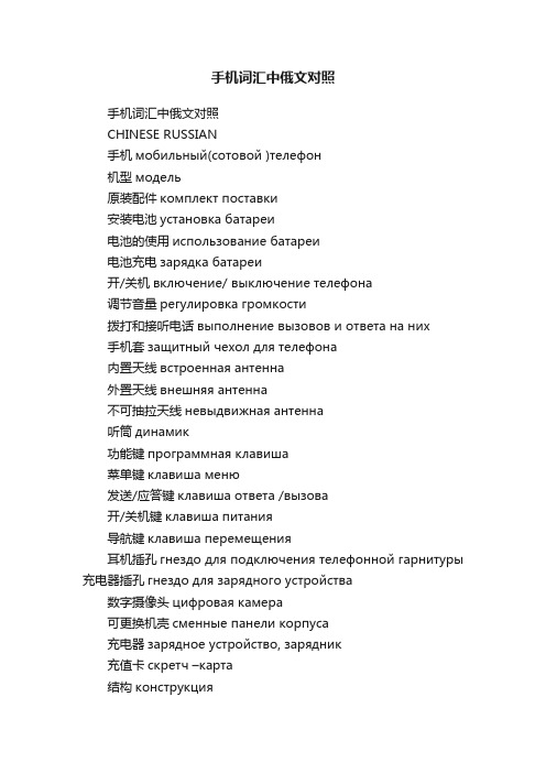
手机词汇中俄文对照手机词汇中俄文对照CHINESE RUSSIAN手机мобильный(сотовой )телефон机型модель原装配件комплект поставки安装电池установка батареи电池的使用использование батареи电池充电зарядка батареи开/关机включение/ выключение телефона调节音量регулировка громкости拨打和接听电话выполнение вызовов и ответа на них手机套защитный чехол для телефона内置天线встроенная антенна外置天线внешняя антенна不可抽拉天线невыдвижная антенна听筒динамик功能键программная клавиша菜单键клавиша меню发送/应答键клавиша ответа /вызова开/关机键клавиша питания导航键клавиша перемещения耳机插孔гнездо для подключения телефонной гарнитуры充电器插孔гнездо для зарядного устройства数字摄像头цифровая камера可更换机壳сменные панели корпуса充电器зарядное устройство, зарядник充值卡скретч –карта结构конструкция机壳外形:折叠式/翻盖тип корпуса: раскладной.с флипом屏幕(彩屏)дисплей(цветной)屏幕清晰度(宽×高)(像素)разрешения дисплея(Ш×В), (пикс)按键кнопка行数количество строек防尘防潮пылевлагостойкость耐击性ударопрочность电池类型тип батареи电池容量(毫安)?мкость батареи(мАч)天线类型тип антенны新聊天室новый чат聊天室名称имя чата呼叫对方вызов партн?ра呼叫号码вызывать номер到最前переход в начало到最后переход в конец聊天内容текст сеанса聊天记录журнал сеанса обмена сообщениями 清除记录очистка журнала结束聊天закончить чат网内通话внутрисетевой переговор网际通话междусетевой переговор漫游роуминг, доставка звонков自动漫游автоматическая доставка звонка来电входящие звонки已接电话полученные (принятые)звонки未接电话пропущенные звонки已拨电话исходящие звонки号码速记блокнот存储号码сохранить номер通话时间время работы в режиме разговора通话指示индикатор?в работе?漫游指示индикатор роуминга信号强度指示индикатор уровня сигналов文字输入指示индикатор ввода текста信息未读指示индикатор ожидающего сообщения电池电量指示индикатор уровня заряда батареи退出键клавиша выхода编辑键клавиша редактирования待机时间время работы в режиме ожидания菜单меню选取выбор阅读читать删除удалить查看смотреть回拨ответ调用вывод最近拨出电话последние набранные номера已接来电принятые номера未接来电не отвеченные номера锁定键盘заблокировать клавиатуру输入создать通讯录телефонный справочник查看通讯录条目просмотр записи справочника存储通讯录条目сохранение записи в справочнике语音提示录制通讯录речевая метка для записи справочника拨听通讯录中的号码набор номера из справочника编辑通讯录条目редактирование записи справочника通讯录条目排序сортировка записей справочника复制通讯录条目копирование справочника检查通讯录容量проверка ?мкости справочника我的电话号码мои номера短信息сообщение新信息новоесообщение文字信息текстовые сообщения图片浏览器картинки или просмотр изображений信息服务информационные службы信息明细параметры сообщения已发短信息список при?ма待发短信息список отправки已读信息прочитанное сообщения未读信息непрочитанное сообщения编写信息составление сообщения发送短信息послать сообщение重复发送повтор отправки发送中выполняется отправка发送失败доставка не выполнена已发送доставлено保存短信息сохранение сообщения删除信息удаление сообщения阅读信息чтение сообщения锁定信息блокировка сообщения短信息服务功能设定параметры小区广播短信息трансляция短信息存储собственная память на SMS短信息写入简化系统система упрощения ввода SMS预制短信息SMS-заготовки快捷方式быстрый доступ发信箱исходящие сообщения收件箱входящие сообщения草稿箱черновики存入草稿箱сохранить в черновиках呼叫等待режим удержания呼叫服务сервис звонков呼叫时间таймеры разговора呼叫费用стоимость вызова数据计时器время данных数据量объ?мы данных通话计时таймер разговора末次通话计时последний вызов累计通话计时все вызовы主叫号码显示идентификация限制本机号码显示передавать ID计费设定стоимость разговора呼叫转移переадресация语音呼入голосовые вызовы传真呼入факсовые вызовы数据呼入посылка данных取消所有设定отменить вс?查看已设状态статус保密авторизация保密设置защита手机锁блокировка телефона锁定键盘блокировка клавиатуры锁定应用блокировка приложения解锁键盘разблокировка клавиатуры禁止呼叫блокировка вызова更改密码новые пароли固定拨号фиксированный набор设机锁定блокировка телефона呼叫限制запрет вызовов转移状态состояние переадресации全部取消отменить вс?手机状态состояние телефона本机号码мой телефонный номер选择线路активная линия电池电量индикатор батареи其他信息другие сведения拨号限制功能запретить вызов新网络новая сеть搜索方式режим поиска网络清单список сетей用户设定персонификация选择语言язык鸣音功能тоны时钟功能функция часов鸣音模式параметры сигналов显示设置установка дисплея车载в автомобиле问候语приветствие默认设定值предустановка单键速拨功能горит клавишный набор充值пополнение сч?та记事簿записная книжка群组功能группировка списка абонентов铃声数量количество типов звонков和弦полифонические мелодии自编和弦数目количество программируемых мелодий呼叫振动вибровызов秒表секундомер倒计时器таймер обратного отсч?та通话时长计时器таймеры продолжительного разговора通话时长语音提示звуковая сигнализация продолжительного разговора货币换算конвертер валют自动键盘锁автоматическая блокировка клавиатуры个人电脑接口подключение к ПК内置调制解调器встроенный модем蓝牙Bluetooth ,синий зуб录音,语音记事диктофон内置FM调节器встроенный FM-тюнер内置MP3播放器встроенный MP3 плеерJava 支持поддержка Java-приложений游戏数目количество встроенных игр支持BMP格式图片поддержка картинок в формате BMP支持Midi格式的和弦铃声поддержка мелодий в формате Midi俄文菜单/记事本русификация(или русское ) меню俄文WAP русификация WAP辅助信息вспомогательная информация收/发俄文短信息русификация входящих SMS /исходящих SMS 语音拨号вызов голосом声控拨号голосовой набор语音指令(指令数量)управление голосом (количество команд)语音邮件,语音留言голосовая почта语音信箱голосовой ящик媒体中心медиа - центр主题тема我的铃声мои мелодииMoto 混音器синтезатор мелодий MotoMixer 铃音类型стили звонки高音铃音высокий звонок轻柔铃音тихий звонок振动вибровызов静音бесшумный工具箱офисные средства日程表ежедневник游戏игры选择并开始新游戏выбор и запуск новой игры结束游戏прекращение игры游戏规则правила игры游戏等级уровень игры通话设置настройка In-Call呼叫费用设置настройка стоимости вызова本机号码限制мой идентир-тор通话与传真разговор и факс应答选项параметры ответа初始设置исходная настройка时间与日期время и дата单键拨号набор в одно касаниеTTY设置настройка TTY背景光подсветка滚动прокрутка动画анимация省电模式экономия батареи主清除общая очистка主复位общий сброс调节对比度настройка контрастности其它设置другие настройки个性化персонализация主菜单главное меню颜色样式цветовая палитра屏幕保护заставка快速拨号ускоренный набор问候语персональное приветствие选择提示铃音выбор звонка и сигнала оповещения自动应答автоматический ответ车载设置настройка для авто服务拨号вызов служб选择提示模式выбор профиля оповещения使用免提настройка телефона для использования без помощи рук通话管理управление вызовами发送双音多频音отправка сигналов DTMF网络功能сетевые функции查看手机使用情况сведения об использование телефона。
安卓内置APK程序中英文对照表

*AllowUsbDebuggingCritically.apk 不可删除,不知道是什么程序,但是估计和USB连接电脑有关.建议不删除。
AntHalService.apk 选删,无线电服务,跟收音机相关ApplicationsProvider 选删,搜索应用提供商,删除后不能与电脑进行电话本同步等操作*atfwd.apk 不可删除,未知,我没有删,不知道有什么用的.BackupAndRestore。
apk 选删,备份与恢复,不重要,感觉没啥用。
BackupRestoreConfirmation.apk 选删,备份还原,不用谷歌备份的留着没啥用BackupRestoreRemoteService。
apk 选删,备份恢复远程服务,与上面两个关联BasicDreams.apk 选删,休眠模式2、BlackGestureCustom.apk 选删,建议不删, 黑屏手势,双击开屏,黑屏打开闪光灯等都要这个Blacklist.apk 选删,来电拦截,用第三方的可以删除BluetoothExt 选删蓝牙相关Browser 选删,游览器,可以用第三方C2U.apk 选删,虽然不知道什么用,但是我没用删除,看看大小54KB。
还是不删除吧。
CABLService.apk 选删,有的说是传感相关有的说是自动调整亮度,但是个人建议不删除。
Calculator 选删,计算器Calendar.apk 选删,日历。
CalendarProvider。
apk 选删,日历相关,用来添加在日历中添加的事项,备忘等,日历删了就删除吧~CertInstaller.apk 选删,建议不删除.证书服务,证书再比如使用移动支付这一类可能就会需要删除他主进程后依然会主动加载,不过也不会奔溃,点击设置里面的证书服务会FC Clock 选删,时钟,如果需要闹钟,建议不删。
*com。
qualcomm。
location.apk 不可删除。
高能CPU情景模式,不能删除.删除后CPU一直工作在固定频率*Contacts 不可删除, 联系人*ContactsProvider 不可删除联系人存储,不能删除,否则不能保存电话本DayD 删除,看看大小54KB.还是不删除吧。
HBC-GoogleAndroid

C ASE : SM-176D ATE : 07/28/09Amanda Silverman and Christof Wittig, with the assistance of David Hoyt, prepared this case under the supervision of Professor Robert A. Burgelman as the basis for class discussion rather than to illustrate either effective or ineffective handling of an administrative situation.Copyright © 2009 by the Board of Trustees of the Leland Stanford Junior University. All rights reserved. To order copies or request permission to reproduce materials, e-mail the Case Writing Office at: cwo@ or write: Case Writing Office, Stanford Graduate School of Business, 518 Memorial Way, Stanford University, Stanford, CA 94305-5015. No part of this publication may be reproduced, stored in a retrieval system, used in a spreadsheet, or transmitted in any form or by any means –– electronic, mechanical, photocopying, recording, or otherwise –– without the permission of the Stanford Graduate School of Business.G OOGLE ’S A NDROID : W ILL IT S HAKE UP THE W IRELESSI NDUSTRY IN 2009 AND B EYOND ?We want people out there to use the Internet on their phones a lot. It actually doesn’t matter if itis Android, the iPhone or something else. —Sergey Brin, Cofounder, Google 1I NTRODUCTIONOn September 24, 2008, Open Handset Alliance (OHA) partners Google and T-Mobile reached a milestone. They unveiled the T-Mobile G1, the first mobile phone to use Google’s Android open source operating system. The phone was due to ship in a month’s time.2Since the Alliance came together in November 2007, consumers and industry participants speculated about the impact Android would have on the wireless market, and whether Google’s participation would disrupt the industry landscape. An analyst explained, “I am not sure people are going to be lining up at stores for this device. The iPhone was a game changer from a consumer perspective. The Google phone may be more of a game changer from an industry perspective.”3 Some industry participants even felt that the iPhone was the important trigger event, as it provided an extremely user-friendly interface and easy Internet access, while Android was simply riding in its wake.Rich Miner, manager of Google’s mobile platform group, also contemplated the question of what would come of Android. He wondered whether Google and its OHA partners would achieve the success they each had planned by their participation in Android. Had they put together an 1 Miguel Helft and Saul Hansell, “Google Introduces an iPhone Rival Open to Whims,” The New York Times , September 24, 2008. 2 Ibid. 3 Ibid.ecosystem that would result in a rich source of mobile applications, an unparalleled mobile Internet experience, and the breakaway success of Android-enabled smartphones?G OOGLE’S E NTRY I NTO M OBILE T ELECOMMUNICATIONSAt the end of 2007, Google was the largest search engine on the Internet. The company’s core search engine product maintained an index of data gathered from web sites, news sites, images, books, and other global sources, and organized this information, making it freely available to its users. Larry Page and Sergey Brin originally founded the company while studying together at Stanford University in September 1998. In 2001, Eric Schmidt was brought on as the new CEO, and in 2004, the company went public. In 2008, Google reported revenues of $21.8 billion, compared to $16.6 billion in 2007. The vast majority of revenue (99 percent in 2007 and 97 percent in 2008) came from the company’s core advertising products, which appeared on Google’s search pages. (See Exhibits 1-3 for Google financial data, forecasted revenue, and biographies of Schmidt, Page, and Brin.)Google’s principal product was Adwords, a service in which companies, or advertisers, could purchase ads space on Google sites and its advertising networks. Companies who advertised using this service paid only when web users clicked on their ads.4 Adsense was a related service, in which partners, or companies with their own websites, joined the Adsense network. Through the program, these partners relied on Google to provide them ad content, which they would place on their own websites. The partners split the proceeds of banner advertisements placed with Google. Fees included payments on a per click and per impression basis.5 In addition to these core products, Google was expanding its product portfolio, in part through an aggressive acquisition strategy that began in 2001 and included notable acquisitions like YouTube (video content) and Google Maps (interactive maps).6Google’s New Growth Opportunity in Mobile TelecommunicationsGoogle’s interest in mobile telecommunications was driven by the explosive growth in mobile subscribers, and the development of mobile technology to enable a wide range of new mobile applications.By 2007, there were 3.5 billion mobile phone subscribers worldwide and the base was expected to grow to 5.4 billion by 2011.7,8 (See Exhibit 4 for mobile phone subscribers by geography.) In4 “Adwords,” Google website, /select/Login (September 28, 2008).5 Per click fees were paid when a user clicked on an advertisement. Per impression fees were paid when an advertisement appeared on a web page viewed by a user.6In addition to Adsense and Adwords, Google’s product portfolio included: Google Talk (instant messaging product); Froogle (comparison shopping services); Google Images (online image library); Google Video and YouTube (video content); Google News (news feeds); Google Finance (financial news and information); Google Maps (interactive maps); Google Groups (Internet discussion groups); Gmail (free e-mail service), Orkut (social networking), Blogger (a web-based publishing tool for blogs), and Google Apps (free, hosted word processing and spreadsheet applications).7 “Phoning, the World Over,” , October 25, 2007, /2007/10/25/mobile-market-subscription-technology-personaltech-cz_1025mobilemap.html, (January 26, 2009).2007, 1 billion handsets had shipped and volumes were expected to grow to 1.9 billion handsets by the end of 2012, representing a compound annual growth rate of 13.5 percent over the period.9 By 2007, while the subscriber base in the Americas, including the U.S., represented around 20 percent of subscribers worldwide, this market accounted for 40 percent of the total worldwide market by value as measured by revenues from handset sales.10,11 (See Exhibit 4 for subscribers by geography and Exhibit 5 for global market segmentation by value.)Demand for particular phone models varied by geography and wealth class. In emerging markets, most consumers acquired low-end mobile phones to simply access basic voice telephony services, and sometimes also cherished their mobile device as an affordable luxury and a symbol of status. Demand for a new type of high-end mobile phone, the so-called “smartphone” (further discussed later in this case), emerged from a new segment of wealthier and better educated customers who began to perceive the mobile phone as a pocketable computer, which could potentially replace all other portable electronic devices. The smartphone segment accounted for around 13 percent of all mobile phones sold in 2008.12 Worldwide sales for smartphones were expected to grow to 619 million in 2012.13 (See Exhibit 6 for yearly forecasts of worldwide smartphone unit sales.) Google saw an extraordinary growth opportunity in facilitating new types of advertising on these devices.Google’s Strategic Intent in Mobile TelecommunicationsGoogle had already begun offering mobile services in 2001. At that time, several wireless markup languages, such as “wireless application protocol” (WAP), enabled Google’s services to be accessed through a mobile phone’s Internet browser.14 These languages were used to translate standard websites into websites compatible with mobile phone browsers. While available on a mobile device, it was generally understood by industry experts that these websites were unsuitable for the small screen size and slow connection speeds of these devices, or they were too limited to offer a compelling user experience.By July 2007, Google had begun testing mobile ads with its U.S. partners, websites that enrolled in its Adsense online advertising program. The company announced:As part of our efforts to develop new and improved AdSense products for ourpartners, we will begin a limited beta test for AdSense for mobile. AdSense for8 “Worldwide Mobile Subscriber Forecast,” Shosteck Group and Mobile World, October 31, 2007, /071031-141648.html (January 26, 2009).9 “Global Mobile Phones: Industry Profile,” DataMonitor, December 2008.10 Ibid.11 In 2007, the global mobile phone market was valued at $114.3 billion. “Global Mobile Phones: Industry Profile,” DataMonitor, December 2008.12 “Smartphones – Smart Revenues,” Juniper Research, February 2009.13Roberta Cozza, “Forecast: Smartphones by Operating System, Interface and End User Segment, Worldwide, 2006-2012,” Gartner, December 11, 2008.14 WAP browsers provide access to WAP sites or websites that are written or dynamically converted to WML, the Wireless Markup Language. WAP, or Wireless Application Protocol, is the open international standard for the application layer that enables wireless communication, mainly access to the Internet, from a mobile phone.mobile allows publishers to monetize their mobile websites through the placementof targeted text ads. Publishers can take advantage of the fast-growing mobileadvertising market and benefit from our targeting technology.15On November 5, 2007, Google announced its partnership in the Open Handset Alliance (discussed in more detail later in this case). In January 2008, Google participated in the Federal Communications Commission’s (FCC) 700 MHz spectrum auction, unexpectedly placing a bid of $4.5 billion for the spectrum. The 700 MHz spectrum became available as part of the switch to digital television, making frequencies once used for analog television broadcasting available for other uses.16Meanwhile, Google also led an effort to bind together advocacy groups and lobby the FCC to adopt open-access rules that would require the winner of the spectrum auction to allow any device or application to connect over the spectrum. While Google lost the bid to Verizon, the FCC ultimately gave in to Google’s lobby, requiring Verizon to adopt open access for the awarded spectrum. Industry experts suggested that Google gained what the company may have wanted from their participation in the auction, a fast, open network for all its applications and services, including Android-based devices. Following the auction, Verizon announced that it would open its existing mobile network to any cell phone and allow subscribers to run third-party applications on their phones beginning in November.17During December 2007, traffic to Google’s mobile services surged from a new subscriber base using the Apple’s iPhone, surpassing traffic levels from any other type of mobile device,18 though at the time iPhone users accounted for just 2 percent of smartphones worldwide compared to Symbian’s 63 percent.Later, in August 2008, Google’s Schmidt described the opportunity to make money in mobile computing, as contrasted to its revenues at the time which were primarily in desktop, saying: “We can make more in mobile than [in] desktop eventually. The reason is because the mobile computer is more targeted. Think about it, you carry your phone everywhere. It knows all about you. We can do a very, very targeted ad. Over time, we will make more money from mobile advertising.”1915 Stephen Wellman, “Google Tests Mobile Version of AdSense for the U.S.,” , July 15, 2007,/blog/main/archives/2007/07/google_tests_mo.html;jsessionid=AXMO2AQZKDH34QSNDLOSKH0CJUNN2JVN, (September 28, 2008).16 “About Lower 700 MHz,” FCC, /services/index.htm?job=about&id=lower700, (May 14, 2009).17 Elinor Mills, “Spectrum Auction: Google Wins by Losing,” CNET News, March 20, 2008, /8301-10784_3-9900190-7.html, (November 30, 2008).18 Miguel Helft, “Google Sees Surge in iPhone Traffic,” The New York Times, January 14, 2008, /2008/01/14/technology/14apple.html (September 28, 2008).19 Henry Blodget, “Google Still Dreaming of $50 Billion Mobile Ad Market,” , August 13, 2008, /2008/8/google-dreaming-of-50-billion-mobile-ad-market, (September 28, 2008).A NDROID AND G OOGLEAndroid began as a start-up company developing an open source operating system for digital cameras. However with its purchase by Google, and the later formation of the Open Handset Alliance, the mission evolved to delivering an open source operating system for smartphone devices.Early DaysAndroid began as a stand-alone company founded by Andy Rubin and Chris White. They were developing an operating system for digital cameras, but had difficulty demonstrating the market need, and in securing financing. Meanwhile, Rich Miner was working at Orange Ventures, a venture capital group associated with Orange, a part of France Telecom. There, he observed the need for carriers to have a new, more powerful handset platform that could be deeply branded. It also needed to be truly open. At Orange, he had worked on the Microsoft Windows Mobile launch with some of his portfolio companies, and noted that “Microsoft was dictating what apps you could and couldn’t have on the handset and the extent that the handset could be customized. We had no ability to get source code to fix bugs or influence the platform in any significant way.”20At the time, the industry was not well positioned to deliver on this opportunity. Miner commented, “The carriers felt they were losing their ability to influence some of the larger handset OEMs or platform providers. And the handset OEMs themselves felt they were not in a position where they could deliver on the carriers’ expectations for the handsets they wanted.” The current open source Linux operating system was not sufficient to remedy the problem. What began as one version of free Linux became 20 different versions licensed by different companies. The result was a fragmented environment, where one company’s Linux handset was completely different from another’s, and very complex integration tasks were required in order to compete with mainstream platforms like Windows and Symbian.Soon, Miner met with Rubin, who had started to wonder if his idea of an open operating system was more suitable for the mobile phone than the digital camera. They began to retarget the Android effort toward the mobile phone. Miner recalled:We jelled very quickly on a unified vision―that having an open, powerful,advanced mobile phone platform that we could get adopted by a lot of the handsetOEMs by being very open―was important. And it was at a time when there waspull from carriers. The handset OEMs also needed it because they were beingpushed by the carriers to deliver powerful handsets with carrier-based brandingand e-branding.2120 Quotations from interviews with the authors, unless otherwise specified.21 E-branding is branding on the Internet, with the primary tool being the corporate website.Google Acquisition and Open Handset AllianceIn July 2005, the team sold Android to Google and stayed on after the acquisition. Much speculation ensued as Android remained a stealth project until November 2007, when Google led the unveiling of the Open Handset Alliance (OHA), and made the announcement of Android as an open source mobile operating system for smartphone devices. Distinct from LiMo,22 whose Foundation’s members were collaborating to build its operating system, the OHA members were furnished with Android as a completed operating system.23 As part of the announcement, Schmidt stated:This partnership will help unleash the potential of mobile technology for billionsof users around the world. A fresh approach to fostering innovation in the mobileindustry will help shape a new computing environment that will change the waypeople access and share information in the future. Today’s announcement is moreambitious than any single ‘Google Phone’ that the press has been speculatingabout over the past few weeks. Our vision is that the powerful platform we’reunveiling will power thousands of different phone models.24The OHA had 34 partners including mobile carriers, chipset and handset manufacturers, and application providers. (See Exhibit 7 for a listing of members.) Most prominent were China Mobile, the world’s largest carrier by subscribers, T-Mobile, Intel, Motorola, HTC, Qualcomm, and Samsung. Nokia, the dominant handset manufacturer, and AT&T and Vodafone, both major carriers, did not join the Alliance initially. An announcement stated the group’s mission: This alliance shares a common goal of fostering innovation on mobile devices andgiving consumers a far better user experience than much of what is available ontoday’s mobile platforms. By providing developers a new level of openness thatenables them to work more collaboratively, Android will accelerate the pace atwhich new and compelling mobile services are made available to consumers.25Android Developer CommunityOn November 13, 2007, the first release of the Android software development kit (SDK) became available for free download. As an open source rather than proprietary operating system, the development community could build mobile applications that could run on smartphones that had Android installed on them, without any hurdles to obtaining access to the SDK and the Application Developer Interfaces (APIs), or paying a license fee for shipping the software on the devices with the respective operating system. Typical developer SDKs in the industry usually required expensive certification and often high membership fees. License fees of comparable 22 LiMo was a version of Mobile Linux, and was supported by the LiMo Foundation, which was established in January 2007.23 Richard Adhikari, “LiMo and Android: Is This Town Big Enough for Both?,” LinuxInsider, February 14, 2008, /story/61685.html?wlc=1240252610, (April 20, 2009).24 “Industry Leaders Announce Open Platform for Mobile Devices,” Google website, November 5, 2008, /intl/en/press/pressrel/20071105_mobile_open.html (September 28, 2008).25 Ibid.operating systems retailed at $0.50 to $25.00 per handset shipped, which were paid by manufacturers.The SDK included the entire software package needed to operate the hardware of an Android-enabled mobile handset, and allowed for advanced features through powerful APIs, including location-based services and data portability.26 Compared to other platforms, the development community characterized Android by its ease of use; programming for the Android was analogous to that of a PC or the web. In contrast to Symbian, which was often regarded by industry participants as an odd development environment for experts only, Android offered one that was compelling even for current college graduates who had been programming on Linux and Java and using open source tools.27 Key features appealed to developers as well; these included the always-on Internet and location-aware services, including GPS, which worked like a compass recognizing the subscribers’ geographical position. Altogether, the SDK offered the average software developer, trained in the popular Java software programming language, the ability to write and test simple mobile applications in a matter of days.In addition, chipset providers that built the components managed by the Android operating system could use the open standard to develop very powerful reference platforms. Reference platforms were akin to an implementation template for a chipset for a typical phone, without requiring a full implementation. Chipset designers often used these for testing, deriving their own implementations, and understanding the best design approach. Thus, they would be able to bring up new chipsets with greater ease and better performance on a level playing field.With the release of the Android SDK, Google also announced a $10 million Android Developer Challenge, during which a panel of industry judges would select the best applications written for Android devices. Within less than three months, 500,000 copies of the SDK had been downloaded. The first of two separate $5 million challenge events took place from January to August 2008, with submissions due by April 2008, and plans for 50 finalist teams, including ten $275,000 and ten $100,000 prize winners. The first Challenge was intended to give developers an “opportunity to explore their ideas using the early SDK, and build prototypes,” while the second Challenge would give developers a chance to polish their applications once the mobile handset hardware became available.28 By August, plans for the Android application marketplace (“Android Market”) were announced.Unveiling the First Android PhoneAs noted earlier, in September 2008, Google and T-Mobile unveiled the G1, the first smartphone with the embedded Android operating system. It was forecasted that Android-enabled smartphones would account for 30 percent of Linux enabled smartphone shipments worldwide in 2009 and grow to 80 percent by 2012.29 At the unveiling, Rubin, now Google’s senior director 26 A location-based service (LBS) is a mobile service that makes use of the geographical position of the device. Data portability is the ability to control, share, and move data from one system to another.27 Information based on interviews by the author (Silverman) with industry personnel.28 “Android – an Open Handset Alliance Project,” Google Website, /android/roadmap.html (September 28, 2008).29 Roberta Cozza, op. cit.of mobile platforms, remarked, “Google was obviously a company that was founded on the Internet. It’s the Internet that provides collaboration, openness, and that, of course, yields innovation. With Android, today, we’re bringing some of those advances and strategies to the mobile phone.”30However, Google had much to do before achieving its vision of success for Android. Miner described this vision:We really want to see Android adopted by a very large percentage of mobilehandsets, especially ones that are more feature-rich handsets. The goal is thatthere are a billion-plus mobile phones sold every year and Google would like tosee the majority of those being a very powerful and great phone, [with a]connected data experience, and be very open. That’s the reason we’re makingthis investment.By 2008, Google claimed not to have a business model of its own for Android. Google was clear, however, that it would always bundle its dominant Internet search engine firmly into the fabric of this ecosystem, driving traffic and advertising revenue. Google believed that the future was about phones that were not only great for communication, but were also highly connected data devices. Google claimed it simply wanted to have the opportunity to compete on a level playing field, and the ability to compete on its strengths of technical superiority.Creating a level playing field also meant removing the restrictions imposed by the proprietary platforms, such as their reluctance to provide access to source code to fix bugs, strong control over the development of the platform, and making it difficult for carriers to provide a deeply brandable handset. For example, while Orange (part of French Telecom) worked with Windows Mobile, Microsoft dictated which applications would and would not be on the handset and to what extent the handset could be customized. With these restrictions removed, Android could compete on best-in-class products, as well as by building a strong developer community with a common open standard and a single Android market, where developers could launch their applications to the world.31 While removing entry barriers to the mobile industry would, in principle, drive innovation, it would also challenge traditional business models of some technology start-ups. For example, by giving away a free browser, called “Chrome,”32 for Android, Google would make it unsustainable for startup companies such as Opera, Access, or Openwave to charge a licensing fee for their mobile browser clients, undermining the ability of these firms to attract funds for further innovation.30 “Introducing T-Mobile G1 with Google,” T-Mobile website, September 23, 2008, /g1-announcement.aspx, (September 28, 2008).31 Interview with Rich Miner, Google.32 Chrome was a free, open source web browser developed by Google, and first released in a beta version in September 2008. Google Press Release, “Google Chrome, A New Take on the Browser,” September 2, 2008 (/intl/en/press/pressrel/20080902_chrome.html (July 21, 2009).T HE M OBILE I NDUSTRY L ANDSCAPE IN 2008The mobile communications industry comprised companies from various sectors, including mobile telecommunications operators or carriers, mobile handset manufacturers, chipset manufacturers, software providers, and application developers.Providing Mobile Services in the U.S. MarketWireless services revenues for the U.S.-based mobile carriers in the second quarter of 2008 were around $39 billion, with data service accounting for 21 percent of revenues.33 Traditionally, the consumer obtained wireless services by subscribing to a plan offered by the carriers. Carriers often competed for customers by providing better wireless coverage and reselling the latest mobile devices at a deep, subsidized discount. In 2007, over 70 percent of U.S. mobile subscribers obtained their handset through their carrier, with much of the cost subsidized by the operator. Most carriers viewed offering the phone at a reduced price as strategic in retaining control of the channel to the customers. The expense was simply considered part of the customer acquisition cost, and carriers usually believed they could make up for the loss in the recurring fees from monthly service subscriptions.In addition to this customer acquisition cost, carriers had to recoup their investments for costly mobile network infrastructure. For example, T-Mobile, launched an “Enhanced Data rates for GSM Evolution” (EDGE) network to support data services in 2005, and acquired new spectrum licenses in 2006 for $4.18 billion.34,35,36 By 2007, U.S. carriers had spent $24 billion on wireless infrastructure to provide better territorial coverage, additional spectrum, and upgrades to newer generation networks with higher and faster data transmission capacities.In order to get a good return on these major investments, the carriers sought to increase their average revenue per user (ARPU)—particularly the wireless data ARPU, since they had to contend with decreasing wireless voice ARPU. From 2004 to 2007, the average wireless data ARPU among top U.S. carriers (Sprint, Verizon, and AT&T) increased from $3 to $10 per month, while the average wireless voice ARPU declined from $55 to $42.50.37 (See Exhibit 8 for ARPU and other statistics for major U.S. wireless carriers.) Fees from early data services add-ons, such as downloadable ring tones and Java games, provided carriers with an initial opportunity to supplement revenues from voice minute plans.The carriers provided this new mobile content to subscribers, who used so-called “feature phones,” through their own portals. For example, Verizon spent $35 billion on its network33 Stacey Higginbotham, “More Proof That the Internet Will Save Wireless Carriers,” GigaOM, August 11, 2008, /2008/08/11/more-proof-that-the-internet-will-save-wireless-carriers/, (September 28, 2008).34 EDGE, a digital mobile phone technology that allows improved data transmission rates, is an extension of the top standard Global Systems for Mobile communications (GSM), and is backward-compatible.35 “Wireless Telecommunications Carriers in the US: 51332,” IBISWorld, February 2, 2009.36 T-Mobile was awarded 120 Advanced Wireless Service (AWS) spectrum licenses in the 1700 MHz and 2100 MHz frequency bands, for which the company paid $4.18 billion. “Wireless Telecommunications Carriers in the US: 51332,” IBISWorld, February 2, 2009.37US Wireless Data Market, March 2008.。
Android毕设外文资料和译文

东北大学东软信息学院专业:计算机科学与技术(嵌入式软件开发方向)班级:计嵌入式000000姓名:XXXX学号:08111XXXXX指导教师:XXXX 教授2011 年12 月18 日译文这篇文档主要讲述 An droid 应用框架的核心原则。
站在高层来说,以用户为中心来设 计良好的交互程序,对于应用设计者或是开发者来说是非常重要的。
下面用例子来阐述了 activities 和tasks 的一些底层原则和机制,例如导航,多任 务,activity 重用,意图和activity栈。
这篇文档也着重讨论了一些设计决策,针对如何利用好它们去设计你的应用程序UI 。
这篇文档中的例子均是An droid 应用程序,包括默认应用程序 (比如拨号器)、Google应用程序(比如地图)。
你可以自己在 An droid 模拟器上或是 An droid 手机上去试验这些例 子。
如果你使用An droid 手机试验时,可能未提供本文档中的某些例子。
App lications, Activities, Activity Stack and Tasks理解An droid 系统中的四个基本概念对你是很有帮助的,它们分别是:App licati ons (应用)Activities(活动)Activity Stack (活动堆栈)Tasks (任务)App licati ons一个An droid 应用程序其实就是由一个或者多个Activity 组成。
它们被捆绑在一起并存放进.apk 文件中,这就是 An droid 应用程序。
An droid 中有着丰富的应用程序,比如邮 件、日历、地图定位、文本消息、联系人、照相机、打电话、音乐播放器,系统设置等应 用。
一般情况下,桌面上都会有 An droid 应用程序快捷图标,用户可以选择某一个图标来启动应用程序。
ActivitiesActivity 是An droid 应用程序的主要组成部分,activity 可以是你自己创建的,当然, 。
android各国语言对应的缩写

android各国语⾔对应的缩写android资源⽂件夹的写法规则: 语⾔缩写-国家地区缩写语⾔缩写藏语:bo_CN en英⽂ en_US英⽂ (美国) ar阿拉伯⽂ ar_AE阿拉伯⽂ (阿拉伯联合酋长国) ar_BH阿拉伯⽂ (巴林) ar_DZ阿拉伯⽂ (阿尔及利亚) ar_EG阿拉伯⽂ (埃及) ar_IQ阿拉伯⽂ (伊拉克) ar_JO阿拉伯⽂ (约旦) ar_KW阿拉伯⽂ (科威特) ar_LB阿拉伯⽂ (黎巴嫩) ar_LY阿拉伯⽂ (利⽐亚) ar_MA阿拉伯⽂ (摩洛哥) ar_OM阿拉伯⽂ (阿曼) ar_QA阿拉伯⽂ (卡塔尔) ar_SA阿拉伯⽂ (沙特阿拉伯) ar_SD阿拉伯⽂ (苏丹) ar_SY阿拉伯⽂ (叙利亚) ar_TN阿拉伯⽂ (突尼斯) ar_YE阿拉伯⽂ (也门) be⽩俄罗斯⽂ be_BY⽩俄罗斯⽂ (⽩俄罗斯) bg保加利亚⽂ bg_BG保加利亚⽂ (保加利亚) ca加泰罗尼亚⽂ ca_ES加泰罗尼亚⽂ (西班⽛) ca_ES_EURO加泰罗尼亚⽂ (西班⽛,Euro) cs捷克⽂ cs_CZ捷克⽂ (捷克共和国) da丹麦⽂ da_DK丹麦⽂ (丹麦) de德⽂ de_AT德⽂ (奥地利) de_AT_EURO德⽂ (奥地利,Euro) de_CH德⽂ (瑞⼠) de_DE德⽂ (德国) de_DE_EURO德⽂ (德国,Euro) de_LU德⽂ (卢森堡) de_LU_EURO德⽂ (卢森堡,Euro) el希腊⽂ el_GR 希腊⽂ (希腊) en_AU 英⽂ (澳⼤利亚) en_CA 英⽂(加拿⼤) en_GB 英⽂ (英国) en_IE 英⽂ (爱尔兰) en_IE_EURO英⽂ (爱尔兰,Euro) en_NZ英⽂ (新西兰) en_ZA英⽂ (南⾮) es 西班⽛⽂ es_BO西班⽛⽂ (玻利维亚) es_AR西班⽛⽂ (阿根廷) es_CL西班⽛⽂ (智利) es_CO西班⽛⽂ (哥伦⽐亚) es_CR西班⽛⽂ (哥斯达黎加) es_DO西班⽛⽂ (多⽶尼加共和国) es_EC 西班⽛⽂ (厄⽠多尔) es_ES西班⽛⽂ (西班⽛) es_ES_EURO 西班⽛⽂ (西班⽛,Euro) es_GT西班⽛⽂ (危地马拉) es_HN西班⽛⽂ (洪都拉斯) es_MX西班⽛⽂ (墨西哥) es_NI西班⽛⽂ (尼加拉⽠) et爱沙尼亚⽂ es_PA西班⽛⽂ (巴拿马) es_PE西班⽛⽂ (秘鲁) es_PR西班⽛⽂ (波多黎哥) es_PY西班⽛⽂ (巴拉圭) es_SV西班⽛⽂ (萨尔⽡多) es_UY西班⽛⽂ (乌拉圭) es_VE西班⽛⽂ (委内瑞拉) et_EE爱沙尼亚⽂ (爱沙尼亚) fi芬兰⽂ fi_FI芬兰⽂ (芬兰) fi_FI_EURO芬兰⽂ (芬兰,Euro) fr法⽂ fr_BE 法⽂(⽐利时) fr_BE_EURO法⽂ (⽐利时,Euro) fr_CA法⽂ (加拿⼤) fr_CH法⽂ (瑞⼠) fr_FR法⽂ (法国) fr_FR_EURO法⽂ (法国,Euro) fr_LU法⽂ (卢森堡) fr_LU_EURO法⽂ (卢森堡,Euro) hr克罗地亚⽂ hr_HR克罗地亚⽂ (克罗地亚) hu匈⽛利⽂ hu_HU匈⽛利⽂ (匈⽛利) is冰岛⽂ is_IS冰岛⽂ (冰岛) it意⼤利⽂ it_CH意⼤利⽂ (瑞⼠) it_IT意⼤利⽂ (意⼤利) it_IT_EURO 意⼤利⽂ (意⼤利,Euro) iw希伯来⽂ iw_IL希伯来⽂ (以⾊列) ja⽇⽂ ja_JP⽇⽂ (⽇本) ko朝鲜⽂ ko_KR朝鲜⽂ (南朝鲜) lt⽴陶宛⽂ lt_LT⽴陶宛⽂ (⽴陶宛) lv拉托维亚⽂(列托) lv_LV拉托维亚⽂(列托) (拉脱维亚) mk 马其顿⽂ mk_MK马其顿⽂ (马其顿王国) nl荷兰⽂ nl_BE荷兰⽂ (⽐利时) nl_BE_EURO 荷兰⽂ (⽐利时,Euro) nl_NL荷兰⽂ (荷兰) nl_NL_EURO荷兰⽂ (荷兰,Euro) no挪威⽂ no_NO挪威⽂ (挪威) no_NO_NY挪威⽂ (挪威,Nynorsk) pl波兰⽂ pl_PL波兰⽂ (波兰) pt葡萄⽛⽂ pt_BR葡萄⽛⽂ (巴西) pt_PT葡萄⽛⽂ (葡萄⽛) pt_PT_EURO葡萄⽛⽂ (葡萄⽛,Euro) ro罗马尼亚⽂ ro_RO 罗马尼亚⽂ (罗马尼亚) ru 俄⽂ ru_RU 俄⽂ (俄罗斯) sh塞波尼斯-克罗地亚⽂ sh_YU塞波尼斯-克罗地亚⽂ (南斯拉夫) sk斯洛伐克⽂ sk_SK斯洛伐克⽂ (斯洛伐克) sl斯洛⽂尼亚⽂ sl_SI斯洛⽂尼亚⽂ (斯洛⽂尼亚) sq阿尔巴尼亚⽂ sq_AL阿尔巴尼亚⽂ (阿尔巴尼亚) sr塞尔维亚⽂ sr_YU塞尔维亚⽂ (南斯拉夫) sv瑞典⽂ sv_SE瑞典⽂ (瑞典) th泰⽂ th_TH泰⽂ (泰国) tr⼟⽿其⽂ tr_TR⼟⽿其⽂ (⼟⽿其) uk乌克兰⽂ uk_UA乌克兰⽂ (乌克兰) zh中⽂ zh_CN中⽂ (中国) zh_HK中⽂ (⾹港) zh_TW中⽂ (台湾)android在android⼯程的对应关系:中⽂(中国):values-zh-rCN中⽂(台湾):values-zh-rTW中⽂(⾹港):values-zh-rHK英语(美国):values-en-rUS英语(英国):values-en-rGB英⽂(澳⼤利亚):values-en-rAU英⽂(加拿⼤):values-en-rCA英⽂(爱尔兰):values-en-rIE英⽂(印度):values-en-rIN英⽂(新西兰):values-en-rNZ英⽂(新加坡):values-en-rSG英⽂(南⾮):values-en-rZA阿拉伯⽂(埃及):values-ar-rEG 阿拉伯⽂(以⾊列):values-ar-rIL 保加利亚⽂: values-bg-rBG加泰罗尼亚⽂:values-ca-rES捷克⽂:values-cs-rCZ丹麦⽂:values-da-rDK德⽂(奥地利):values-de-rAT德⽂(瑞⼠):values-de-rCH德⽂(德国):values-de-rDE德⽂(列⽀敦⼠登):values-de-rLI 希腊⽂:values-el-rGR西班⽛⽂(西班⽛):values-es-rES 西班⽛⽂(美国):values-es-rUS 芬兰⽂(芬兰):values-fi-rFI法⽂(⽐利时):values-fr-rBE法⽂(加拿⼤):values-fr-rCA法⽂(瑞⼠):values-fr-rCH法⽂(法国):values-fr-rFR希伯来⽂:values-iw-rIL印地⽂:values-hi-rIN克罗⾥亚⽂:values-hr-rHR匈⽛利⽂:values-hu-rHU印度尼西亚⽂:values-in-rID意⼤利⽂(瑞⼠):values-it-rCH意⼤利⽂(意⼤利):values-it-rIT ⽇⽂:values-ja-rJP韩⽂:values-ko-rKR⽴陶宛⽂:valueslt-rLT拉脱维亚⽂:values-lv-rLV挪威博克马尔⽂:values-nb-rNO荷兰⽂(⽐利时):values-nl-BE荷兰⽂(荷兰):values-nl-rNL波兰⽂:values-pl-rPL葡萄⽛⽂(巴西):values-pt-rBR葡萄⽛⽂(葡萄⽛):values-pt-rPT 罗马尼亚⽂:values-ro-rRO俄⽂:values-ru-rRU斯洛伐克⽂:values-sk-rSK斯洛⽂尼亚⽂:values-sl-rSI塞尔维亚⽂:values-sr-rRS瑞典⽂:values-sv-rSE泰⽂:values-th-rTH塔加洛语:values-tl-rPH⼟⽿其⽂:values--r-rTR乌克兰⽂:values-uk-rUA越南⽂:values-vi-rVN缅甸语: values-my(补充⼀种新语⾔)声明欢迎转载,但请保留⽂章原始出处:CSDN:⾬季o莫忧离:Language English Name ChineseNameCode GB ICS JB KKاﻟﻌﺮﺑﻴﺔArabic(Israel) 阿拉伯语(以⾊列)ar_IL Y Y Y Y Arabic(Egypt) 阿拉伯语(埃及) ar_EGGD_MN GD_MN GD_MN GD_MN中⽂ChineseSimplified中⽂简体zh_TW Y Y Y YChinese Tradition 中⽂繁体zh_CN Y Y Y YChinese 中⽂(⾹港)zh_HK N N72/82/92 GD_MNNederlands Dutch(Netherlands) 荷兰语nl_NL Y Y Y Y Dutch(Netherlands)荷兰语(⽐利时)nl_BEGD_MN GD_MN GD_MN GD_MNEnglish English(UnitedStates)英语(美国)en_US Y Y Y YEnglish(Australia) 英语(澳⼤利亚)en_AUGD_MN GD_MN GD_MN GD_MNEnglish(Canada) 英语(加拿⼤)en_CAGD_MN GD_MN GD_MN GD_MNEnglish(India) 英语(印度)en_INGD_MN GD_MN GD_MN GD_MNEnglish(Ireland) 英语(爱尔兰)en_IEGD_MN GD_MN GD_MN GD_MNEnglish(NewZealand)英语(新西兰)en_NZGD_MN GD_MN GD_MN GD_MNEnglish(Singapore) 英语(新加波)en_SGGD_MN GD_MN GD_MN GD_MNEnglish(SouthAfrica)英语(南⾮)en_ZAGD_MN GD_MN GD_MN GD_MNEnglish(UnitedKingdom)英语(英国)en_GBGD_MN GD_MN GD_MNYFrançais French 法语fr_FR Y Y Y Y French 法语(⽐利时)fr_BEGD_MN GD_MN GD_MN GD_MNFrench 法语(加拿⼤)fr_CAGD_MN GD_MN GD_MN GD_MNFrench 法语(瑞⼠)fr_CHGD_MN GD_MN GD_MN GD_MNDeutsch German 德语de_DE Y Y Y Y German 德语(列⽀敦斯登)de_LIGD_MN GD_MN GD_MN GD_MN German 德语(奥地de_ATGD_MN GD_MN GD_MNYDeutschGerman 德语(奥地利) de_ATGD_MN GD_MN GD_MNYGerman 德语(瑞⼠) de_CHGD_MN GD_MN GD_MN GD_MNItaliano Italian 意⼤利语it_IT Y Y Y YItalian 意⼤利语(瑞⼠)it_CHGD_MN GD_MN GD_MN GD_MNProtuguês Portuguese 葡萄⽛语(巴西)pt_BR Y Y Y YPortuguese 葡萄⽛语pt_PT Y Y Y YEspañol Spanish 西班⽛语es_ES Y Y Y YSpanish 西班⽛语(美国)es_USGD_MN GD_MN 72/82/92YBengali 孟加拉语bn_BD Y N N NBengali 孟加拉语(印度)bn_IN Y Y Y Yhrvatski Croatian 克罗地亚语hr_HRGD_MN GD_MN 72/82/92Yčeština Czech 捷克语cs_CZ Y Y Y YDansk Danish 丹麦语da_DK GD_MN GD_MN 72/82/92YελληνικάGreek 希腊语el_GR GD_MNY Y YעבריתHebrew 希伯来语(以⾊列)he_ILGD_MN GD_MN GD_MN GD_MNHebrew 希伯来语(以⾊列)iw_ILGD_MN GD_MNY YHindi 印度语hi_IN Y Y Y YMagyar Hungarian 匈⽛利语hu_HUGD_MNY Y YIndonesian 印度尼西亚语in_ID Y Y Y Y⽇本語の⾔語Japanese ⽇语ja_JPGD_MN GD_MN 72/82/92 GD_MNKorean 韩语(朝鲜语)ko_KRGD_MN GD_MNY YBahasaMelayuMalay 马来语ms_MY Y Y Y YﻓﺎرﺳﯽPerisan 波斯语fa_IR (fa-rIR)Y Y Y YPolski Polish 波兰语pl_PL GD_MN GD_MN 72/82/92Yromâna Romanian 罗马尼亚语ro_ROGD_MNY Y YРусский Russian 俄罗斯语ru_RU Y Y Y Yсрпски Serbian 塞尔维亚语sr_RSGD_MN GD_MN 72/82/92 GD_MNSvenska Swedish 瑞典语sv_SE GD_MN GD_MN 72/82/92YThai 泰语th_TH Y Y Y Y Türkçe Turkey ⼟⽿其语tr_TR Y Y Y YاردوUrdu 乌尔都语ur_PK Y Y Y Y tiếng việt Vietnamese 越南语vi_VN Y Y Y Ycatalá Catalan 加泰隆语(西班⽛) ca_ESGD_MN GD_MN 72/82/92 GD_MNlatviešu Latviesu 拉脱维亚语lv_LVGD_MN GD_MN 72/82/92YLietuvių Lithuanian ⽴陶宛语lt_LTGD_MN GD_MN 72/82/92YNorsk bokmal Norwegian 挪威语nb_NO GD_MN GD_MN 72/82/92YSlovenčina slovencina 斯洛伐克语sk_SKGD_MN GD_MN 72/82/92YSlovenščina Slovenian 斯洛⽂尼亚sl_SIGD_MN GD_MN 72/82/92 GD_MNSlovenščina Slovenian 斯洛⽂尼亚语sl_SIGD_MN GD_MN 72/82/92 GD_MNбългарски bulgarian 保加利亚语bg_BGGD_MN GD_MN 72/82/92Yукраїнська Ukrainian 乌克兰语uk_UAGD_MN GD_MN 72/82/92YTagalog Filipino 菲律宾语tl_PHGD_MNY Y YSuomi Finnish 芬兰语fi_FI GD_MN GD_MN 72/82/92YAfrikaans Afrikaans 南⾮语af_ZA NGD_MN GD_MN GD_MNRumantsch Romansh 罗曼什语(瑞⼠) rm_CHGD_MN GD_MN GD_MN GD_MNBurmese(Zawgyi) 缅甸语my_ZG N N 72/82/92 N Burmese 缅甸语my_MM N N Y Y Khmer 柬埔寨语km_KH N N Y YAmharic 阿姆哈拉语(埃塞俄⽐亚)am_ET NGD_MN GD_MN GD_MNбеларуская Belarusian ⽩俄罗斯语be_BY NGD_MN GD_MN GD_MNeesti Estonian 爱沙尼亚语et_EE NGD_MN 72/82/92 GD_MNKiswahili Swahili 斯⽡希⾥语(坦桑尼亚)sw_TZ NGD_MN GD_MN GD_MNisiZulu Zulu 祖鲁语(南⾮) zu_ZA NGD_MN GD_MN GD_MNazərbaycanca Azerbaijani 阿塞拜疆语az_AZ N N NGD_MNՀայերէնArmenian 亚美尼亚语(亚美尼亚)hy_AM N N72/82/92 GD_MNქართულიGeorgian 格鲁吉亚语(格鲁吉亚)ka_GE N N NGD_MNລາວLaotian ⽼挝语(⽼挝) lo_LA N N NGD_MNМонгол Mongolian 蒙古语mn_MN N N NGD_MNNepali 尼泊尔语ne_NP N N NGD_MNқазақ тілі Kazakh 哈萨克语kk_KZ N N72/82/92NSinhala 僧加罗语(斯⾥兰卡) si_LK N N NGD_MN1、标记“ N ”表⽰当前版本不⽀持;标记“ Y ”表⽰mtk、google均⽀持;标记“ GD_MN ”表⽰Google默认⽀持,MTK不⽀持。
Android系统应用程序中英文对照表
htccalendarwidgetsHTC日历桌面小插件
HTCCamera照相机(没人想把它删了吧)
HtcClockWidget闹钟小插件
HtcCompressViewer
HtcContacts联系人
CertInstaller证书安装器(貌似不能删)
CheckinProvider签入服务
Clicker键盘校准(貌似是)
com.htc.FMRadioWidget桌面收音机插件(插件类都可以删,自己决定)
com.htc.FriendStreamWidget好友流小插件(可删)
com.htc.MusicWidget桌面音乐插件
HtcScreenTimeoutWidget.apk调节屏幕延时插件
HtcSettingsProvider.apk HTC设置
htcsettingwidgets.apk HTC设置小插件,WIFI、移动网络、GPS、飞行模式、蓝牙的开关(好用)
HTCSetupWizard.apk HTC安装向导
GoogleFeedback谷歌反馈(反馈啥,直接干掉)
GooglePartnerSetup Google助手(直接干掉)
GoogleQuickSearchBox谷歌搜索(删了影响到桌面的搜索插件,自启动,干掉他)
GoogleServicesFramework谷歌同步支持服务框架(删了不能同步联系人,不能登录google,我留着呢)
HtcPushMedia.apk
pk
HtcRecommendsWidget.apk
HtcRingtoneTrimmer.apk铃声剪辑(无视,删了)
安卓APK程序中英文对照表
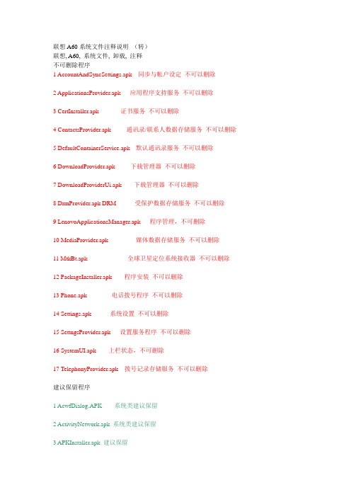
联想A60系统文件注释说明(转)联想, A60, 系统文件, 卸载, 注释不可删除程序1 AccountAndSyncSettings.apk 同步与帐户设定不可以删除2 ApplicationsProvider.apk 应用程序支持服务不可以删除3 CertInstaller.apk 证书服务不可以删除4 ContactsProvider.apk 通讯录/联系人数据存储服务不可以删除5 DefaultContainerService.apk 默认通讯录服务不可以删除6 DownloadProvider.apk 下载管理器不可以删除7 DownloadProviderUi.apk 下载管理器不可以删除8 DrmProvider.apk DRM 受保护数据存储服务不可以删除9 LenovoApplicationsManager.apk 程序管理,不可删除10 MediaProvider.apk 媒体数据存储服务不可以删除11 MtkBt.apk 全球卫星定位系统接收器不可以删除12 PackageInstaller.apk 程序安装不可以删除13 Phone.apk 电话拨号程序不可以删除14 Settings.apk 系统设置不可以删除15 SettngsProvider.apk 设置服务程序不可以删除16 SystemUI.apk 上栏状态,不可删除17 TelephonyProvider.apk 拨号记录存储服务不可以删除建议保留程序1 AcwfDialog.APK 系统类建议保留2 ActivityNetwork.apk 系统类建议保留3 APKInstaller.apk 建议保留4 CellConnService.apk 系统类建议保留5 Bluetooth.apk 蓝牙(删了就没有蓝牙了)建议保留6 Calculator.apk 计算器(自带计算器较弱,可用其他替代)7 CameraOpen.apk 自带相机(用360的可删)8 Contacts.apk 通讯录/联系人(用第三方通讯录的可删)9 DataDialog.apk 数据对话框不确定,没删10 EngineerMode.apk 工程师模式不确定,没删11 EngineerModeSim.apk sim卡模式,建议保留12 fmradio.apk 收音机(可删)13 Gallery3D.apk 相机相框(可删)14 Launcher2.apk 主题,可用其他主题替换15 LenovoSDAC.apk 系统相关,建议保留16 LenovoClock.apk 自带闹钟(用第三方闹钟的可删)17 LenovoSystemInformation.apk 系统信息,建议保留18 Mms.apk 自带信息(可删,用第三方短信的就删了吧19 MobileLog.apk 可删除20 ModemLog.apk 可删除21 Music.apk 自带音乐(可删,换成其他播放器)22 SmsReg.apk sms存储,建议保留23 Provision.apk 开机引导程序24 v*p*nServices.apk v*p*n服务(v*p*n服务,建议保留)25 YGPS.apk GPS相关,建议保留可删除程序1 116114.apk 联通的116114,可删除2 A8MusicWidget.apk 音乐播放,可删除3 Browser.apk 谷歌浏览器(喜欢UC的可用UC替代)4 Calendar.apk 日历(不用日历的可删)5 CalendarProvider.apk 日历(不用日历的可删)6 Citynum.apk 来电地区查询,可删除7 FileBrowser.apk 文件管理,不用可删除,也可用第三方替代8 Email.apk email(不用自带email接受邮件的可删)9 FilterList.apk 防扰助手,类似防火墙,可删除。
A new high-speed high resolution open-loop CMOS sample and hold

A new high-speed,high-resolution open-loop CMOS sample and holdAlireza Abolhasani •Mohammad Tohidi •Khayrollah Hadidi •Abdollah KhoeiReceived:16September 2012/Revised:8May 2013/Accepted:11September 2013/Published online:25September 2013ÓSpringer Science+Business Media New York 2013Abstract A new open loop,high resolution CMOS sample and hold (S/H)circuit is introduced in this article.This circuit is constructed based on a new method which leads to a great reduction in dependency of the storing charge of the holding capacitors to the charge injection of transistors.It is a combination of dummy switches and auxiliary capacitors in order to decrease the voltage spikes that are produced during the sampling mode.Due to the high linearity feature of our proposed design in comparison with previous works,it is reached to a great improvement in signal to noise and distortion ratio up to about 15dB and it’s ENOB is equivalent with about 16bits.Another advantages of our proposed design are it’s lower power dissipation and it’s high input voltage range.Also the optimum functionality of our proposed circuit does not damaged by the threshold voltage’s variations in different corners.As our proposed S/H circuit has been designed in open loop structure,it is suitable for high speed applications.Keywords Sample and hold circuit ÁHigh linear ÁHigh speed sampling ÁAnalog to digital converter1IntroductionNowadays,as the demand for high speed signal processing applications such as medical imaging and broadband communications,efforts have been focused on improving functionality of their constitutive elements.One of these key elements is the analog to digital converter (ADC).Achieving to a high speed highly resolution ADC requires a great improvement on its structure and fundamental blocks.Sample and hold circuits are one of these compo-nents.Improving the speed and the linearity of the sample and hold circuits upgrades the speed and resolution of ADCs.Different methods are utilized to design S/H cir-cuits.One of these methods is the closed-loop structure.As this structure includes the feedback loop,its speed and stability considerations confront with great limitations.Also,due to the lack of buffering capability of these S/H structures,it is required to utilize switched-capacitor architectures to construct the ADCs with these S/H circuits.It should be noted that these ADCs have the speed limitation.Another prominent method is the open loop structure.The most important advantages of these structures are their simple architecture,high speed operation and also main-taining with wide range of inputs,as explicated in [1,2,3].A major disadvantage of the open loop structure is its relatively poor linearity.A modification is applied in [3]to improve the linearity;however its linearity is limited,too.In the proposed circuit in this article,high intrinsic linearity is obtained by utilizing dummy transistors to remove the voltage spikes during sampling mode.The rest of this article is organized as follows:Sect.2concentrates on the previous works.Section 3presents the proposed design and its advantages.Section 4illustrates the simulation results and gives a brief comparison ofA.Abolhasani (&)ÁM.Tohidi ÁK.Hadidi ÁA.Khoei Microelectronics Research Laboratory,Urmia University,Urmia,Irane-mail:a.abolhasany@ M.Tohidie-mail:m.tohidi.urmia@ K.Hadidie-mail:kh.hadidi@urmia.ac.ir A.Khoeie-mail:a.khoie@urmia.ac.irAnalog Integr Circ Sig Process (2014)78:409–419DOI 10.1007/s10470-013-0158-zprevious works with proposed design.Finally,Sect.5 includes the concluding remarks in thefinal section.2Previous works2.1Closed loop structureAs shown in Fig.1,a closed-loop sample and hold circuit that relies on negative loop feedback is introduced.This structure leads to a highly linear functionality in compar-ison with open loop cases.As the sampling switch is located inside the feedback loop,so,the voltage swing of sampling switch is much smaller than output and input voltage swings.This interest reduces the nonlinearity of sampling switch’s functionality,too.Although this archi-tecture is suitable for high linear cases,but due to the utilizing of the negative loop feedback,it requires the compensation that causes inherent limitations to use of this architecture in high-speed applications.As depicted in Fig.1and by considering C hold as a miller capacitance at the output of G m amplifier,the dominant pole of S/H circuit which is located in node X is equivalent with:P Dominant¼12p r o C hold1þA0ðÞð1Þwhere r o is the output resistance of G m block and A0is open loop DC gain of A block.To obtain the high linear output, this dominant pole should provide enough phase margins. Due to the including of the negative loop feedback in this structure and also,because of contribution of multiple non-dominant poles by both G m and A amplifiers,the compen-sation is obligatory which in turn restricts the speed of this structure,considerably.Also,as the signal path from input to output goes through input capacitances of G m amplifier,so,it causes hold mode feed-through effects that influence on the overall signal to noise ratio of this structure.2.2Open loop structureThe main interests of the open loop structure are its sta-bility and highly potential speed.As the circuit does not rely on any feedback and any considerable compensation, so,it can be utilized for high speed applications.One of the other prominent advantages of utilizing open loop struc-tures are their simplicity;due to the simple buffer structure and utilizing of no feedback,the required area for this simple structure considerably reduces.Also we can reach to a great reduction of power dissipation while obtaining to the high linear and high speed functionalities.Previously, due to the lack of a highly linear open loop buffer in CMOS technology,most of high linear open loop sample and hold architectures were constructed as in BiCMOS process and rely on bipolar devices for high sampling rates[4,5].Later, based on a highly linear CMOS buffer presented in[6]and also based on a passive differential sampling,an open loop CMOS sample and hold circuit proposed in[1]without utilizing of negative loop feedback.The proposed sample and hold circuit achieved to a high sampling rate while maintaining high linearity.Also another new sample and hold architecture was presented in[2]to enhance the lin-earity and speed of the proposed structure in[1]with a great improvement on the functionality of the CMOS buffer’s structure and also,utilizing dummy switches.Atfirst,we discuss about the S/H circuit with input switch sampling and then,we talks about the sample and hold circuit with grand plate sampling.Finally the proposed S/H architecture in[3]will be explained.Figure2shows a basic open loop CMOS S/H circuit.Even with assuming ideal buffers,we consider with two main drawbacks which degrades the linearity of this structure.The main factor is the voltage-dependent charge injection of the input switch.For low and medium input voltage frequencies,the charge injection of the sampling switch is almost equal for both sides and has less dependency to analog input voltage;but for higher frequencies,the sampling switch’s charge is divided according to the impedance that it sees from each side.Thus,the charge injection of input sampling switch on each side is dependent to the input voltage causing odd harmonics at least,which deteriorates the linearity of this structure.Due to this fact,an error voltage is caused which is input dependent.It is assumed that almost the half of the accumulation charge in the gate channel goes through the holding capacitance that is verified by following equations:D V error1¼1=2D QCð2Þand so on,it is obtained as:D V error1¼À1=2ÁW swÁL swÁC oxðV ddÀV inÀV thÞC holdþC diffþC gdð3Þwhere V dd is the supply voltage,V in is the input signal amplitude,V th is the threshold voltage of input NMOS switch,W and L are the width and length of NMOS switch, C ox,C diff and C gd are the gate oxide,drain to bulk and gate to drain capacitors,respectively.It should be noted that the variation of threshold voltage of NMOS switch due to the transistor’s body effects and other process limitations and also the different amounts of input signal amplitude in positive and negative peaks lead to the different values of error voltage,introduced by the charge injection,as shown in Eq.(3).So it can be divided into two parts:1.By the lowest amount of threshold voltage and theinput voltage amplitude in negative peak,the largest amount of error voltage is achieved.2.By the highest amount of threshold voltage and theinput voltage amplitude in positive peak,the smallest amount of error voltage is obtained.As the error voltage produced by the mentioned charge injection is not the same at positive and negative peaks, hence even harmonics are generated too.So,this event degrades the linearity.The next mismatch is the switch driving signal’s influ-ence on the value of holding capacitor through the C gd.It can be named as clock feed-through which generates the second error voltage as following equation:D V error2¼ÀC gdC holdþC diffþC gdV ddð4ÞAs shown in Eq.(4),the value of second error voltage can be reduced by enlarging the holding capacitor.If the second error voltage is decreased by enlarging the holding capacitor and besides,if it is required to obtain the high speed ADCs, the size of NMOS input switch should be enlarged in order to obtain the low sampling time.But according to Eq.(3), enlarging the size of input NMOS switch increases the value of the error voltage which was produced by the injection charge.Also,it causes large parasitic capacitors from the source and drain to gate and bulk nodes as another drawback for the speed of ADCs.So enlarging the holding capacitor and the size of input switch are not suitable for eliminating the mentioned error voltages.If we ignore the values of C gd and C diff versus the value of the holding capacitor by considering it large enough,its value can be estimated.It is similar to a RCfilter.The total resistor thermal noise powerat the output of thefilter is equivalent with P n;out¼KThold ascalculated in[7],where K is the Boltzmann constant,T is the Kelvin temperature and C hold is the holding capacitor.It should be less that at least a square of total error power.Thetotal error power is equivalent with P error¼q212,which is calculated in[8],where q is the one least significant bit andis equivalent with¼V ref2n.V ref is the input voltage’s range and n is the resolution bit.So,the following equations are concluded:KTC hold\14Âq212ð5ÞAnd so on,it is obtained as:C hold[KTÂ48Â22nV2refð6ÞIt should be noted that the input switch have a resistance like role in high frequencies.Due to the variation of threshold voltage and also the different values of negative and positive amplitudes of input analog voltage,the resistance value of the input switch is different in both opposite voltage peaks.So,the size of the input switch should be considered at the best optimized value.Utilizing large switches generates more error voltage that is produced by charge injection.Also,utilizing the smaller switches causes great changes in the value of the resistance of the input switch.So,the value of the mentioned resistance is obtained according to the required precession of the holding capacitor’s settling time.It should be less than the expected resolution of the ADC.So the following equations are admitted:V refÁeÀT=RC hold\V refÁ2Ànð7ÞAnd so on,it is obtained as:R\TC holdÁnÁln2ð8Þwhere T is the conversion time of the ADC.As depicted in Fig.3,a dummy switch is replaced between the input switch and the holding capacitor to alleviate the mentioned problem.To overcome on the error voltage produced by charge injection,it’s size is considered as a half of the input switch’s size and also it is turned on with a little delay after sampling of the input switch.But due to the random mismatch between sampling and dummy switches,and also because of non-equal division of charge injection of input switch,as mentioned before,the perfect cancellation of charge injection is not guaranteed.It should be noted that the error voltage which was produced by clock-feed-through is almost degraded by constructing the input and dummy switches by three unit transistors rather than constructing them with one and two of unit transistors.In this case,as the drain and source of dummy switch areconnected to each other,it’s gate to drain and gate to source capacitors can cancel the contribution of charging coming from the other two unit input transistor’s gate to drain capacitors.So this modification will enhance the performance of the circuit.Finally,it should be noted that if a differential structure is utilized,the even harmonic effects and also many of other nonlinear mismatches that are produced by the input switches will be detracted.As depicted in Fig.4,the open loop sample and hold circuit with ground plate sampling is presented to reduce the error voltage produced by charge injection of the input switches.It is assumed that if sampling switches open slightly before than input switches,there will be no channel to the injection of the charge to the holding capacitors.But in practice,there are drain diffusion capacitors of M0,M1 and M2at nodes X1and X2.Hence the capacitor C eq is obtained after opening these sampling switches which is equivalent capacitor of parasitic capacitors in series with holding capacitor(C hold).Although the error voltage by charge injection is not perfectly eliminated,but it is reduced due to the smaller C eq than C hold.The following equations show the differential error voltage produced by charge injection where a is the uncanceled fraction of it: Vþerror¼Àa C ox WL V ddÀV inþÀV th1ðÞ2C holdVÀerror¼Àa C ox WL V ddÀV inÀÀV th2ðÞ2C holdV errorj j¼VþerrorÀVÀerrorV errorj j¼a C ox WL V inþD V thðÞ2C holdð9Þwhere V in¼VþinÀVÀin;D V th¼V th1ÀV th2:Figure5shows the prior S/H open loop circuit with two auxiliary capacitors which is introduced in[3].The effectof C0hold on removing the charge produced by opening input switches will be explained in the next section.3Our proposed S/H circuitFigure6shows the new proposed sample and hold circuit. Additional dummy switches are utilized in Fig.6in com-parison with the design of[3](shown in Fig.5),to enhance the linearity and resolution of the sample and hold circuit’s output.As shown in proposed work(Fig.6),there is a single differential switch M0as a differential sampler in the circuit which operates at ground potential.When it opens,it produces equal charge injection on both sides.To remove this devastative effect,the dummy switches M1 and M2are utilized.Also the opening of the sampling switches M3and M4at the ground potential injects the charge which is independent from the input voltage and treats as an offset voltage.By using of the switches M5and M6,the value of the mentioned offset voltage is degraded. Also,when M7and M8are opened to remove C0hold capacitors,they create charge injection,too.The error voltage which is produced due to the charge injection leaves deteriorative effects on the sampled and output signal.To alleviate this problem,the dummy switches M9 and M10are utilized.Finally,it should be noted that the most possible amount of voltage spikes derived from the charge injections are degraded inherently by using of the mentioned added switches.3.1Functionality of the proposed structureAs shown in Fig.6,thefirst step is the tracking mode in which all switches are closed and output voltage tracks the input voltage.In the next mode,sampling mode,atfirst M0 is opened and then the dummy switches M1and M2are closed to eliminate the some sort of this single differential switch’s charge injection.Also,M3and M4are opened in this stage that they produce a constant offset voltage due to the generating of the charge injection.Then M5and M6are closed to reduce this deteriorative effect.So,according to the following equations,the destructive effects of injected charge on the output nodes by opening M0,M3and M4 switches are degraded with these dummy switches,where a is the extant fraction of charge:V X1¼Àa C ox WL V ddÀV X1ÀV th1ðÞðC hold jj C0holdÞþC p1¼C holdC holdþC p1Vþerror V X2¼Àa C ox WL V ddÀV X2ÀV th2ðÞðC hold jj C0holdÞþC p2¼C holdC holdþC p2VÀerror V errorj j¼VþerrorÀVÀerror¼a C ox WL V XþD V thðÞðC hold jj C0holdÞþC pð10Þwhere C p=C p1=C p2are parasitic capacitors and V X=V X1-V X2.It should be noted that C hold is considered large enough in comparison with C p.In the next mode,named‘‘input switch opening’’,M11and M12 are opened and then dummy switches M13and M14are closed to cancel a percentage of their charge injection. Also,as shown in Fig.6,two capacitors remain on each side to absorb the remaining charge injection.One of them is C0hold and the other one is C eq which is the equivalent capacitor of C p in series with C hold.Since C eq is much smaller than C0hold,the largest fraction of the charge injection is absorbed by C0hold.So,the following equations verify the great reduction of charge injection error,where a is the uncanceled fraction of the charge injection:V þerror ¼À12a C ox WL V dd ÀV in þÀV th 1ðÞC eqðC 0hold þC eq Þ2V Àerror ¼À12a C ox WL V dd ÀV in ÀÀV th 2ðÞC eqðC 0hold þC eq Þ2V error j j ¼V þerror ÀV ÀerrorV error j j ¼a C ox WL V in þD V th ðÞC eq2ðC 0hold þC eq Þ2ð11Þwhere V in ¼V þin ÀV Àin and D V th ¼V th1ÀV th2:For the next operation,M7and M8are opened toremove the C 0hold capacitors and then M9and M10are closed as dummy switches to remove the effects of charge on output nodes as following equations:V þerror¼À12a C ox WL V dd ÀV th 1ðÞðC 0hold jj C pÞV Àerror ¼À12a C ox WL V dd ÀV th 2ðÞðC 0hold jj C pÞV error j j ¼V þerror ÀV Àerror ¼12a C ox WL D V th ðÞðC 0hold jj C 0pÞð12Þwhere C 0p is the equivalent capacitor of the drain and dif-fusion capacitors of M7and M8after opening.Finally the switches M3and M4are closed and M5and M6are opened to buffering the sampled voltage to the output.3.2Clocking of the proposed S/H circuitAs shown in Fig.6,our proposed S/H circuit requires six clocks to have the optimized function.Figure 7shows the clock generator of our proposed architecture.It is con-structed of same inverters as simple logic gates and only an ‘‘OR’’gate.These entire clock signals have been made from one input clock signal.Also,as shown in Fig.6,we utilize four inverters separately to generate the clock signals of dummy switches M1,M2and M13,M14from the generated clock signals of the clock generator.The simulation results of all generated clock signals by the proposed clock generator are depicted in Fig.8.3.3Buffers of the new proposed S/H circuitWe utilize the two simple buffers that are depicted in Fig.9in our proposed S/H circuit due to their enhanced linearity.They are proposed in [9].The main reason for the distortion of these buffers is the unity gain variation along with the input signal variation.The gain of these buffers is equiv-alent with:A v ¼g m 1Ár ds 1r ds 21þg m 1Ár ds 1r ds 2ð13Þwhere g m is the transconductance of the driver device and r ds is the dynamic drain-source resistance of the driver and the load devices.The variation of the r ds of the driver device along with V in ,is in opposite direction of the variations of the g m of the driver device and the r ds of the load device along with V in .This event causes the product of g m Ár ds to be stayed almost constant.Also according to the given proofs in [3],we can conclude that the g m of the driver devices and the total r ds of the driver and load devices stay almost constant along with the variation of theinput signal.So,the unity gain of this buffer stays almost fixed despite the input signal’s variation.As depicted in Fig.10,the differential output amplitude value of this buffer is945mv when the differential input signal is2V peak to peak.Thus,the nonlinearity effect of these buffers will be negligible on achieved output signals of the new proposed S/H circuit.The only condition is that the length and width of two devices of the buffers should be the same and output bias point should be V out=V dd/2.As shown in Fig.9,the bulk nodes of PMOS driver transistors are connected to their sources.So,the source to bulk voltages of these transistors are equivalent with zero. Consequently,according to the following equation,the body effect is removed[7]:V th¼V th0þcffiffiffiffiffiffiffiffiffiffiffiffiffiffiffiffiffiffiffiffiffiffiffiffi2u FþV SBj jpÀffiffiffiffiffiffiffiffiffiffiffi2u Fj jpð14Þwhere c is the body effect coefficient,V SB is the source to bulk potential difference and u F is the Fermi level.4Comparison and simulation resultsOur proposed S/H circuit,shown in Fig.6,is designed in a 0.18l m poly double CMOS technology.The sizes of uti-lized transistors are given in Table1.As it is shown,the sizes of dummy switches are considered about a half of the sizes of the switches that were injected the charge into the circuit by opening.Also,the sizes of the C0hold capacitors are considered as about a twentieth value of the holding capacitors.All of these considerations are taken in order to degrade the dete-riorative effects of the charge injection and the clock feed-through on the linearity of the new proposed S/H circuit.The holding capacitors are equivalent with1pf in this circuit.The transient outputs of the proposed S/H before and after the buffer is depicted in Figs.11and12respectively,for an input sinusoidal signal of2V p–p with input fre-quency of20MHz and with the sampling frequency of 200MHz.It should be noted that,based on our proposed S/H circuit shown in Fig.6,dummy switches and auxiliary capacitors are utilized to remove the voltage spikes.So,as shown in Fig.11,a great linearity in the proposed S/H circuit’s output is achieved.Figure13shows the output spectra of this circuit’s output and the total harmonic dis-tortion(THD)is reached to a high value as-93.79dB. Also the output is reached to a high resolution with ENOB=15.28bits.To the author’s best knowledge,due to release of the driving problem of the next stage,this linear output should be passed through a buffer.So,the most important factor is the use of a highly linear buffer to overcome the nonlinear effects of the utilized buffer on the output of the proposed S/H circuit.Figure12shows the proposed circuit’s output after buffer.As shown in Fig.14, the utilized buffer has negligible nonlinear effects,since the THD achieves to only-83.9dB,which shows that the THD and linearity remain high enough after passing through the buffer.Also the ENOB degrades a very low amount into13.64bits.Table1Sizes of the transistors used in the S/H circuit Transistor W/L(l m)Transistor W/L(l m)M030/0.18M89/0.18M110/0.18M95/0.18M210/0.18M105/0.18M39/0.18M1120/0.18M49/0.18M1220/0.18M55/0.18M1310/0.18M65/0.18M1410/0.18M79/0.18Figures15and16show the THD and ENOB of the outputs of the proposed S/H circuit,before and after buffer, respectively,for different input frequencies(1,5,20,and 40MHz)and with200MHz sampling frequency.To the author’s best knowledge,the precision of any analog circuit depends on the process variations.The threshold voltage of the CMOS transistors is one of the main factors which can be changed due to the non-uniform doping or thin-oxide thickness.With respect to the‘‘TT’’which stands for typical–typical case,the variation parameters are categorized to four corners as follows:‘‘SS’’corresponds for slow–slow‘‘SF’’corresponds for slow–fast ‘‘FS’’corresponds for fast–slow ‘‘FF’’corresponds for fast–fastIn the mentioned corners,thefirst letter refers to NMOS transistors and second one to PMOS transistors.It should be noted that the threshold voltage has the most and theFig.15THD comparison of the proposed S/H output,before and after buffer,for different input frequencies and200MHz sampling frequencyFig.16ENOB comparison of the proposed S/H output,before and after buffer,for different input frequencies and200MHz sampling frequencyleast values along with the slow and the fast corners, respectively.So it is essential to perform corner analysis. Table2summarizes the results of the four corners for an input sinusoidal signal of1V p–p with input frequency of 20MHz and with the sampling frequency of200MHz.It shows that the new proposed S/H circuit’s functionality is almost invariant by process variations.Another advantage of our proposed S/H circuit is it’s lower power dissipation in comparison with other designs [2].Simulation results by Hspice,demonstrate that the whole power dissipation of the new proposed S/H circuit is about5.8MW at a3.3V power supply for TSMC0.18l m CMOS technology.A summary of the results with a comparison with our prior designs are gathered in Table3. Also,Table4shows the comparison of our work with previous reported works.Table2Corner analysis of the new S/H circuitTHD SNDR ENOBTT-93.7993.9115.28 SS-91.390.914.94 FF-96.49615.7 SF-91.891.7115FS-9595.415.6Table3Dynamic performance of the new S/H and our previous works[2],[3]Sampling rate125MHz200MHz500MHzInput freq.(MHz)220402040This work HD3-109.94-93.91-91.1-82-78 SNDR109.9493.590.5781.277.5ENOB17.9715.2814.7713.413.1 [3]HD3-83-79-76-79-74.3SNDR7976.8707569ENOB–––––[2]HD3-82-80-77-83-80SNDR6864606359.7ENOB–––––Table4Comparison between our new proposed S/H with previous worksWork Structure Tech(l m)Power Fin Fs SFDR SNR SNDR THD(dB)ENOB(bits)This work Open-loop0.18 5.8mw1M200M––106.1-106.4217.385M200M––102.32-102.7416.7720M200M––93.5-93.7915.2840M200M––90.57-90.7114.7720M500M––81.2-81.5413.440M500M––77.5-77.8113.1[10]Closed loop0.13 1.84l w50K1M–72–-408.7[11]Closed loop0.18 6.5mw2M100M–––64.510[12]Close loop0.1812.04l w1kHz128kHz–––-75.9612.62[13]Closed loop0.18 4.15mw10M80M–––-6010[14]Open-loop0.3570mw50M70M 185M–––-62-6210[15]Closed loop0.35 2.6mw 2.5M5M 50M–––-58.2-54.69[16]Closed loop0.356mw 1.3M13M–60–-66–[17]Open-loop0.356mw1M100M–62–-7713[18]Open-loop0.1815mw40M500M62–––9.6[19]Open-loop0.35 3.1mw20M200M––72––40M200M––64––5ConclusionThis paper presents a new open loop S/H circuit.The most prominent advantage of this design are its high linearity and its high speed.Due to the utilizing of auxiliary capacitors and dummy switches in this structure,the most part of the voltage spikes are removed which were pro-duced due to the charge injection,clock feed through or constant error voltages.As a result,a great improvement in signal to noise and distortion ratio(SNDR)up to15dB is obtained.Also,it’s ENOB is equivalent with about16bits. Next,the circuit operates up to200and500MHz of sampling frequencies with the HD3better than-93.91and -82dB,respectively for a2V p–p,20MHz input frequency.References1.Hadidi,K.H.,Sasaki,M.,Watanabe,T.,Muramatsu,D.,&Matsumoto,T.(1998).An open-loop full CMOS103MHz -61dB THD S/H circuit.The IEEE Custom Integrated Circuits Conference(pp.381–3).Santa Clara,USA.2.Hadidi,K.H.,Muramatsu,D.,Oue,T.,&Matsumoto,T.(1999).A500MS/s-54dB THD S/H circuit in a0.5um CMOS pro-cess.25th European solid-state circuits conference(pp.158–61).Duisburg,Germany.3.Mousazadeh,M.,Hadidi,K.H.,&Khoei,A.(2008).A novelopen-loop high-speed CMOS sample-and-hold.AEU Interna-tional Journal of Electronics and Communi-cations,62(8), 588–596.4.Schillaci,L.,Baschirotto, A.,&Castello,R.(1997).A3-V5.4mW BiCMOS track and hold circuit with sampling frequencyup to150MHz.IEEE Journal of Solid-State Circuits,32, 926–932.5.Razavi,B.,&Sung J.(1995).A200MHz BICMOS sample-and-hold amplifier with3V supply.IEEE Internati-onal Solid-state Circuits Conference,Digest of Technical Papers(pp.56–57).San Francisco,CA.6.Hadidi,K.H.,&Khoei,A.(1996).A highly linear cascade driverCMOS source follower buffer.Proceedings of Third Interna-tional Conference on Electronics,Circuits and Systems(pp.128–132).Rodos,Greece.7.Razavi,B.(2001).Design of analog CMOS integrated circuit.McGraw-Hill Series in Electrical and Computer Engineering.8.Razavi,B.(1995).Principles of data conversion system design.New York:IEEE Press.9.Hadidi,K.H.,Sobhi,J.,Hasankhan, A.,Muramatsu, D.,&Matsumoto,T.(1998).A novel highly linear cmos buffer.The5th IEEE International Conference on Electronics,Circuit and Sys-tems(pp.369–71).Lisbon,Portugal.10.Sawigun,C.,&Serdijn,W.A.(2011).Analysis and design of alow-voltage,low-power,high-precision,class-AB current-mode subthreshold CMOS sample and hold circuit.IEEE Transactions on Circuits and Systems I,58,1615–1626.11.Trivedi,R.(2006).Low power and high speed sample-and-holdcircuit.IEEE International Midwest Symposium on Circuits and Systems.MWSCAS‘06.49th,vol.1,pp.453–456.12.Mah,S.L.Chan,P.K.&Mishra,S.K.(2010).A precision low-power mismatch-compensated sample-and-hold circuit for bio-medical applications.IEEE Asia Pacific Conference on Circuits and Systems(APCCAS)(pp.192–195).13.Reddy,Y.S.G.,&Liter,S.(2012).A1.2V80MS/S sample andhold for ADC applications.International Conference on Devices, Circuits and Systems(ICDCS)(pp.15–19).14.Boni,A.,Pierazzi,A.,&Morandi,C.(2001).A10-b185MS/strack-and-hold in0.35l m CMOS.IEEE Journal of Solid-State Circuits,36(2),195–203.15.Lee,T.-S.,&Lu,C.-C.(2005).A1.5-V50-MHz pseudodiffer-ential CMOS sample-and-hold circuit with low hold pedestal.IEEE Transactions on Circuits and Systems I,52,1752–1757.16.Balachandran,G.K.,&Allen,P.E.(2001).Fully differentialswitched-current memory cell with low charge-injection errors.IEE Proceedings Circuits Devices and Systems,148(3),157–163.17.Sugimoto,Y.,&Haigh,D.G.(2008).A current-mode circuitwith a linearized input V/I conversion scheme and the realization of a2/2.5V operational,100MS/s,MOS SHA.IEEE Transac-tions on Circuits and Systems I,55(8),2178–2187.18.Harpe,P.,&Zanikopoulos, A.,Hegt,H.van Roermund,A.(2006).A62dB SFDR,500MSPS,15mW open-loop track-and-hold circuit.24th Norchip Conference(pp.103–106).19.Sadollahy,M.,&Hadidi,K.(2008).High-speed highly-linearCMOS S/H circuit.International Conference on Computer and Communication Engineering(ICCCE)(pp.550–553).Alireza Abolhasani was bornin Urmia,Iran,in1988.Hereceived the B.S.degree inElectrical Engineering fromUrmia Azad University,Iran in2010(with honor)and currently,he is M.S.student of electricalengineering in Urmia Univer-sity.His research interests areanalog and digital integratedcircuit design and DC–DC con-verters for portable applications,fuzzy systems and neural net-works.He is currently withElectrical Engineering Depart-ment and Microelectronics Research Laboratory in Urmia University, Urmia,Iran.Mohammad Tohidi was bornin Urmia,Iran,in1988.Hereceived the B.S.degree inElectrical Engineering fromUrmia University,Iran in2010(with honor)and currently,he isM.S.student of electrical engi-neering in Urmia University.His research interests are analogand digital integrated circuitdesign,fuzzy systems and neu-ral networks.He is currentlywith Electrical EngineeringDepartment and Microelectron-ics Research Laboratory in Ur-mia University,Urmia,Iran.。
- 1、下载文档前请自行甄别文档内容的完整性,平台不提供额外的编辑、内容补充、找答案等附加服务。
- 2、"仅部分预览"的文档,不可在线预览部分如存在完整性等问题,可反馈申请退款(可完整预览的文档不适用该条件!)。
- 3、如文档侵犯您的权益,请联系客服反馈,我们会尽快为您处理(人工客服工作时间:9:00-18:30)。
1 什么是Android1.1 主要技巧和思想●历史的嵌入式器件编程●开放手机联盟的解释●第一眼看到Android的主屏幕可以这么说,暂时,传统的桌面应用程序开发者已经被惯坏了。
这个不是说桌面应用程序开发比其他形式的开发很简单。
总之,作为传统桌面的应用程序开发者,凡是我们能想象到的各种应用程序,我们就一定有能力创造。
包括我自己,因为我也是从做桌面程序开始的。
一方面已经使得桌面程序更容易理解就是我们已经有能力去跟桌面操作系统相互作用,因此,任何底部的硬件很自由的相互作用。
这种类型独立自主的程序编制,然而,对于很小的开发者团体来说是不敢冒险的去搞手机发展这样浑浊的技术的。
注解:我提到两种不同的开发商在此讨论:传统的桌面应用程序开发,他们能在任何语言环境下工作,而且最终的产品和程序是用来运行“桌面”操作系统的;还有Android 程序开发者,那些开发Android平台开发工具的JAVA程序开发人员。
这不是说跟其他人比起来谁好谁坏。
其实,区别目的仅仅在于想说明并比较Android桌面操作系统环境的开发风格,工具。
1.2 嵌入式器件编程的简要历史有很长一段时间,手机的开发者由大的著名嵌入式的开发团队中的少数人组成,作为嵌入式设备的开发者。
相对于桌面开发或者后续的网络开发,被视作更少“魅力”,而且嵌入式设备的开发通常因为硬件和操作系统而处于劣势。
因为嵌入式设备的制造商们太小气,他们要保护他们硬件方面的秘密,所以他们给开发者们非常有限的库去运行当他们尝试去让一些特定的设备去相互作用。
嵌入设备与桌面系统显著不同的一部分是嵌入设备是个有特色的“芯片上的电脑”。
例如:考虑你的标准电话遥控。
这个并不是一个非常强大并且复杂性的技术。
当任何的按钮被按下去,一个芯片解释一个信号以一种方式已经被编程进了这个设备。
这个允许设备知道什么是从输入设备(键盘)来的需要。
并且如何的响应这些命令(比如,打开电视机)。
这个是一个简单的嵌入式设备的编程。
总之,不管你相不相信,像这样的简单设备绝对的和早期的手机设备开发的根源有着紧密的联系。
大多数的嵌入式设备运行(有些仍然还在运行)在私有的操作系统。
原因是选择创建一个私有的操作系统而不是用任何消费系统是产品的需要。
简单的设备不需要非常健全和优化的操作系统。
作为一个产品的演化,更多复杂的嵌入式设备,如早期的PDA,家庭安全系统和GPS 等。
5年前某种程度上都转移标准的操作系统平台上。
小的操作系统如Linux,甚至一个微软版本的嵌入式平台,已经在嵌入设备上变得普遍了。
设备改革的这段时间里,手机从其他嵌入式设备中分支出去。
走上了自己的轨道,这个分支是显而易见的当你去调查他们的体系结构。
在他们最初开始的时候,手机作为一个外围设备并且运行私有软件,而这些软件被制造商们所拥有和控制,而且几乎可以被认为是一个“关闭”的系统。
习惯使用私有操作系统主要是制造商自己开发硬件,或者至少定义了开发的目的只是用来运行手机。
最终的结果就是使开放成为不可能。
现有的软件包或者解决方案会可靠的和他们的硬件交互。
而且,制造商想要保护他们硬件的商业秘密。
以防允许进入而发现设备软件的水准。
所以风尚就是,而且大多数仍然是使用完全私有并且关闭的软件来运行他们的设备。
任何人想为手机开发程序必须需要详尽的私有环境来运行软件的知识。
而解决方案就是直接从制造商那里购买昂贵的开发工具。
这就孤立了很多的“自制软件”的开发者。
注解:一个关于自制软件开发的文化包含了手机程序的开发。
“自制软件”是指开发者通常不是工作在手机开发公司内,通常利用自己的时间在他们的设备上生产小的,一次性的产品。
另外,使手机开发无法出手的是硬件制造商对于“内存和需要”左右为难的解决方案。
直到最近,手机才能执行比打出和接听电话,查找联系人,发送和接收短消息。
不是今天“瑞士军刀”的技术。
及时在2002年,在消费者的手上,带照相机的手机还是不多见。
在1997年,小的应用程序如计算器和游戏爬进了手机内,但是强大的功能仍然是手机的拨号盘本身。
手机还不想今天一样是一个多用途,多功能工具。
没有人预见互联网浏览的需求,MP3播放,或者更多的是我们今天定制的功能。
在1997年,手机制造商们没有预见消费者需要的是一个一体化的设备。
但是,即使这个需求展现出来,设备内存和存储容量还是一个需要克服的大的障碍。
更多的人可能想要他们的设备是一个多功能一体化的工具,但是制造商们不许跨越他们的障碍。
让问题变得简单,就要在任何的设备让内存来存储并运行程序,包括手机。
手机作为一个设备,直到最近还没有足够多内存来执行“额外”的程序。
在最近的两年里,内存的价格已经达到了非常低的水平。
设备制造商们有足够的能力压低价格来包含更多的内存。
很多的现在的手机标准内存已经超过了90年代中期电脑内存。
于是,现在我们有需求,而且有内存。
我们可以直接跳到为手机开发酷的应用程序了,对吗?不完全是这样。
设备的制造商们仍然紧密的保护他们的操作系统。
有一些在手机上开放JAVA为基础的小运行环境。
更多的是不允许。
即使允许运行JAVA应用程序但还是不允许进入核心的系统。
而这些是桌面开发者习惯于拥有的。
1.3 开放手机联盟和Android这个对于应用程序开发的障碍开始在2007年的11月份被打破,当Google在开放手机联盟下发布Android。
开放手机联盟是一个硬件和软件开发者的集合,包括谷歌,NTT DoCoMo, Sprint Nextel和HTC。
他们的目标是创建一个更多的开放手机环境。
在开放联盟第一个被发布的产品就是移动设备操作系统Android。
(更多关于开放手机联盟的信息,见:)。
对于这个Android的发布,谷歌使很多开发工具和向导成为可能来帮助在新系统上可能的开发者。
帮助系统,平台软件开发包(SDK),甚至一个开发者的论坛,可以在谷歌的Android的网站上找到,/android.这个网站应该是你的起点,而且我极度推荐你去访问。
注解:谷歌为了推动这个新的Android操作系统,甚至为寻找新的Android程序而设立了1000万美元的奖金。
当手机运行Linux, Windows或者即使Palm OS的手机是很容易找到,如本文所述,没有硬件平台已经宣告可以来运行Android.HTC,LG电子,摩托罗拉和三星都是开发手机成员,在Android的发布下,我们希望在不久的将来有一些Android为基的设备。
在2007年11月发布时,系统自身还仍旧是一个测试版的程序。
这是个对开发者的好新闻因为它给了我们一个罕见的提前看到将来的设备和有机会来开始开发应用程序,而当硬件发布时就可以运行。
注解:这个策略明确的给了开放手机联盟一个大的优势,超越其它手机操作系统开发者。
因为当第一代设备发布时会有数不尽的可用开发程序可以运行。
1.4 介绍AndroidAndroid,作为一个系统,是一个运行在Linux2.6核心上的JAVA基础的操作系统。
系统是非常轻量型的而且全特性。
Android应用程序用JAVA开发而且很容易被放置到新的平台上。
如果你没有下载JAVA或者不确定那一个版本你需要,我在第二章详细列出了开发环境的安装。
其他Android的特点包括一个加速3-D图形引擎(基于硬件支持),被SQLite推动的数据库支持,和一个完整的网页浏览器。
如果你熟悉JAVA编程或者是任何种类的OOP开发者,你可能使用程序用户接口(UI)开发-那就是,UI安置是直接在程序代码中有句柄的。
Android,识别并许可UI开发,而且支持新生,XML为基础的UI布局。
XMLUI 布局对普通桌面开发者是一个非常新的概念。
我会在本书的相关章节里描述XMLUI布局和程序化UI开发。
Android另一个更令人激动和关注的特点是因为它的样式,第三方应用程序---包括“自制的”---会和系统捆绑的有着同样的优先权。
这是和大多数系统不同之处,但是给了嵌入式系统程序一个比由第三方开发者创建的线性优先权大的优先执行权。
而且,每一个应用程序在虚拟计算机上以一个非常轻量的方式按照自己的线路执行。
除了大量的SDK和成型的类库可以用之外,对激动人心的特性对于Android的开发者来说是我们现在可以进入到操作系统可以进入的地方。
也就是说,如果你要创建一个应用程序打一个电话,你已经进入到电话的拨号盘。
加入你要创建一个应用程序来使用电话内部的GPS(如果安装了),你已经进入了。
对于开发者创建动态和令人好奇的程序已经敞开大门。
Android的一些特征和上面这些可用的特点相同,谷歌已经非常迫切的奉送一些特性。
Android的开发者可以将自己的应用程序和谷歌提供的如谷歌地图和无所不在的谷歌搜索绑在一起。
假设你要写程序在谷歌地图上显示一个来电话者的的位置,或者你要储存一般的搜索结果到你的联系人中。
在Android中,这个门已经完全打开。
2 应用程序:Hello World2.1 主要技巧和思想●创建新的Android项目●用View工作●用一个TextView●修改main.xml文件●在Android虚拟机上运行一个应用程序在这一章中,你将创建你的第一个Android活动,这一章从头到尾的检查应用程序的创建过程,我将给你们演示怎么去创建一个Android项目在Eclipese,在最初的文件里添加代码,并且在Android虚拟机上运行最终的应用程序,在Android环境下运行的最终结果的应用将是一个完全的功能项目实际上,当你看到这一章,你将不止创建一个Android的活动,在计算机编程的传统规定中,你的第一个应用将是典型的Hello World!应用程序,所以在第一节的内容中你将创建一个标准的Hello World!应用程序,仅仅使用一个空白的背景和一个“Hello World!”文本。
然后,为了让您更好的了解该语言,下一节详细的解释Android为了你的Hello World!应用程序自动的产生文件。
在这个活动中你将创建两个重复的过程,每一个都是使用不同技术信息显示在屏幕上,而且你建创建两个不同版本的Hello World!应用程序将展示“Hello World!”信息的画面,这将给你一个很好的介绍关于Android的控制和内部的工作。
注解:你将经常看到“application”和“Activity”相互交换着应用,他们两个之间的不同就是应用程序可以有多个活动,但是一个应用程序必须至少有一个活动。
你的应用程序的每一个窗口或者是屏幕就是一个分开的活动。
因此,如果你创建了一个相当简单的应用程序仅仅使用了一个屏幕的数据(就像在这一章中的Hello World!应用程序),那就只有一个活动,在后来的章节里面你将创建许许多多的活动。
为了确保你可以完全很好的看到Android程序的整体,在第六章你将在Android软件开发包命令行编译在微软windows和Linux环境下同时创建这些应用程序。