LTC6401IUD-20TRPBF中文资料
6400系列产品说明书

66251270-EN - V1.4 - 15/06/1616400 SeriesArt. 6488 - Installation instructionsArt. 6488 4.3" hands free colour display digital videophone
27mm191mm
111mm
BUS1BUS2GND12MGNDVACNO-DOL+DOLGND ALBALPT3PT267812354
ONSW1SW31234ONSW2
PT1
PT4
JP1Fig. 1 DESCRIPTIONAn intelligent hands free videophone using 4.3” full colour active matrix LCD monitor for VX2300.Including 4 buttons “service”, “privacy/bus relay activation”, “door-open/intercommunicating call” and “answer/camera recall” plus 3 LED’s for visual indication of all functions.Adjustments & programmable options: call tone volume on 3 levels (low, medium, high), picture hue, brightness and contrast, call tone melody, number of rings, privacy duration and address. Also includes a local bell function. The Art. 6488 is surface mount.
PUSH BUTTONS (FIG. 1)Service push button.When pressed it links internally the terminals “C” and “NO” on the connection terminals.
仪表芯片资料

符号 VDD(VDDA)—VSS(VSSA)
Tstg Temp Time
定额 -0.2V~4V -0.3V~VDD +0.3V
±2mA -50℃~+ 150℃
300℃ 10 秒
500mW
8.2 推荐工作条件
符号Βιβλιοθήκη 参数VDD电源电压
VSS
电源电压
时钟晶振
XT
外振荡 频率
陶瓷振荡器
石英晶振
测试条条件 所有外围组件及 CPU
17
PT1.7,PSDO,BZ
I/O, O
数 据 输 入 / 输 出 口 , 蜂 鸣 器 输 出 ,OTP 读 / 写 接 口 (PSDO)。
18
PT1.6,SCK
I/O 数据输入/输出口,SPI 通讯输出接口(SCK)。
19
PT1.5,SDO
I/O, O 数据输入/输出口,SPI 通讯输出接口(SDO)。
20
PT1.4,TX
I/O, O 数据输入/输出口,EUART 通讯接口(TX)。
21
PT1.3,RC,TST
I
数据输入口, EUART 通讯接口(RC) ,测验模式致能。
22
PT1.2,SDI
I/O, I 数据输入/输出口,SPI 通讯接口(SDI)。
23
PT1.1 SCE,PSDI,INTI
I/O I
PDF 文件使用 "pdfFactory Pro" 试用版本创建
Dream Tech International
4 应用领域
4.1 自动量程/手动量程掌上型数字多用表。 4.2 自动量程/手动量程名片型数字多用表。 4.3 自动量程笔式数字多用表。 4.4 自动量程钳型表。 4.5 数字面板表。
Lite-On LAMP LED 产品数据手册说明书

Absolute Maximum Ratings at Ta=25℃Values ParameterSymbolR G B Test Condition UnitMin1.603.900.41Typ.Luminous Flux1ΦvMax.3.408.470.99R :I F =25mAG :I F =30mA B :I F =15mA lmViewing Angle 2θ1/2Typ.130R :I F =25mA G :I F =30mA B :I F =15mA °Min618517455Typ.Dominant Wavelength2λdMax.629532465R :I F =25mA G :I F =30mA B :I F =15mAnmTyp.x0.68790.1317~0.21500.1555λd (Min)Typ.y0.31150.68900.0283Typ.x0.70550.0805~0.18250.1443Color Coordinateλd (Max)Typ.y 0.29400.78500.0461R :I F =25mAG :I F =30mA B :I F =15mAMinTyp.628523458Peak WavelengthλpMax.R :I F =25mAG :I F =30mA B :I F =15mAnmMin1.8 3.12.6Typ. 2.23.4 3.0Forward V oltage3V F Max.2.53.55 3.4R :I F =25mA G :I F =30mA B :I F =15mAVReverse Current I RMax.10V R =5VμA Spectrum Radiation Bandwidth∆λTyp.203322R :I F =25mAG :I F =30mA B :I F =15mAnmNote :1.Tolerance of Luminous Intensity +/-10%2.Tolerance of Dominant Wavelength +/-1nm3.Tolerance of Forward Voltage +/-0.1V4.Caution in ESD:Static Electricity and surge damages the LED.It is recommend to use a wrist band or anti-electrostatic glove when handling the LED.All devices,equipment and machinery must be properly grounded.5.CAS140B is the test standard for the chromaticity coordinates IV.Bin Code ListLuminous Spec.TableLuminous Flux (lm)I F :R=25mA,G=30mA,B=15mA Ranks Min.Max.W0 5.91 6.41W1 6.417.05W27.057.76W37.768.53W48.539.38Tolerance on each Luminous Intensity bin is +/-10%Color Ranks TableRanks Color bin limitsI F :R=25mA,G=30mA,B=15mA Ranks Color bin limitsI F :R=25mA,G=30mA,B=15mA x 0.24310.25630.25630.2431x 0.25630.26940.26940.2563H4y 0.21420.21860.22740.2230J4y 0.21860.22300.23180.2274x 0.24310.25630.25630.2431x 0.25630.26940.26940.2563H5y 0.22290.22730.23610.2317J5y 0.22730.23170.24050.2361x 0.24310.25630.25630.2431x 0.25630.26940.26940.2563H6y 0.23170.23610.24480.2404J6y 0.23610.24050.24920.2448x 0.24310.25630.25630.2431x 0.25630.26940.26940.2563H7y 0.24040.24480.25360.2492J7y 0.24480.24920.25800.2536x 0.24310.25630.25630.2431x 0.25630.26940.26940.2563H8y 0.24920.25360.26230.2579J8y 0.25360.25800.26670.2623x 0.24310.25630.25630.2431x 0.25630.26940.26940.2563H9y 0.25790.26230.27110.2667J9y 0.26230.26670.27550.2711x 0.26940.28250.28250.2694x 0.28250.29560.29560.2825K4y 0.22300.22740.23610.2318L4y 0.22740.23170.24050.2361x 0.26940.28250.28250.2694x 0.28250.29560.29560.2825K5y 0.23170.23610.24480.2405L5y 0.23610.24040.24920.2448x 0.26940.28250.28250.2694x 0.28250.29560.29560.2825K6y 0.24050.24480.25360.2492L6y 0.24480.24920.25790.2536x 0.26940.28250.28250.2694x 0.28250.29560.29560.2825K7y 0.24920.25360.26230.2580L7y 0.25360.25790.26670.2623x 0.26940.28250.28250.2694x 0.28250.29560.29560.2825K8y 0.25800.26230.27110.2667L8y 0.26230.26670.27540.2711Bin Code ListColor Ranks TableRanks Color bin limitsI F :R=25mA,G=30mA,B=15mA Ranks Color bin limitsI F :R=25mA,G=30mA,B=15mA x 0.26940.28250.28250.2694x 0.28250.29560.29560.2825K9y 0.26670.27110.27980.2755L9y 0.27110.27540.28420.27980.29560.30870.30870.29560.30870.32180.32180.3087M40.23170.23610.24480.2405N40.23610.24040.24920.2449x 0.29560.30870.30870.2956x 0.30870.32180.32180.3087M5y 0.24040.24480.25350.2492N5y 0.24480.24910.25790.2536x 0.29560.30870.30870.2956x 0.32180.30870.30870.3218M6y 0.24920.25350.26230.2579N6y 0.25790.25360.26230.2666x 0.29560.30870.30870.2956x 0.30870.32180.32180.3087M7y 0.25790.26230.27100.2667N7y 0.26230.26660.27540.2711x 0.30870.29560.29560.3087x 0.32180.30870.30870.3218M8y 0.27100.26670.27540.2798N8y 0.27540.27110.27980.2841x 0.29560.30870.30870.2956x 0.30870.32180.32180.3087M9y 0.27540.27980.28850.2842N9y 0.27980.28410.29290.2886Tolerance on each Hue bin (x,y)bin is +/-0.01.C.I.E.1931Chromaticity DiagramH5H6H7H8H9J5J6J7J8J9K5K6K7K8K9L5L6L7L8L9M5M6M7M8M9N5N6N7N8N9H4J4K4L4M4N40.210.220.230.240.250.260.270.280.290.300.240.250.260.270.280.290.300.310.320.33X-coordinateY -c o o r d i n a t eShipping Label Code ListShipping Label CodeLuminous Flux RanksW0W1W2W3W4H 4A1B1C1D1E1H5A2B2C2D2E2H6A3B3C3D3E3H7A4B4C4D4E4H8A5B5C5D5E5H9A6B6C6D6E6J4A7B7C7D7E7J5A8B8C8D8E8J6A9B9C9D9E9J7A10B10C10D10E10J8A11B11C11D11E11J9A12B12C12D12E12K4A13B13C13D13E13K5A14B14C14D14E14K6A15B15C15D15E15K7A16B16C16D16E16K8A17B17C17D17E17K9A18B18C18D18E18L4A19B19C19D19E19L5A20B20C20D20E20L6A21B21C21D21E21L7A22B22C22D22E22L8A23B23C23D23E23L9A24B24C24D24E24M4A25B25C25D25E25M5A26B26C26D26E26M6A27B27C27D27E27M7A28B28C28D28E28M8A29B29C29D29E29M9A30B30C30D30E30N4A31B31C31D31E31N5A32B32C32D32E32N6A33B33C33D33E33N7A34B34C34D34E34N8A35B35C35D35E35C o l o r R a n k sN9A36B36C36D36E36CAUTIONS1.ApplicationThe LEDs described here are intended to be used for ordinary electronic equipment(such as officee q u i p m e n t,c o m m u n i c a t i o n e q u i p m e n t a n d h o u s e h o l d a p p l i c a t i o n s).C o n s u l t L i t e o n’s S a l e s in advance forinformation on applications in which exceptional reliability is required,particularly when the failure or malfunction of the LEDs may directly jeopardize life or health(such as in aviation,transportation,traffic control equipment,medical and life support systems and safety devices).2.StorageThis product is qualified as Moisture sensitive Level3per JEDEC J-STD-020Precaution when handing this moisture sensitive product is important to ensure the reliability of the product.The package is sealed:The LEDs should be stored at30°C or less and90%RH or less.And the LEDs are limited to use within one year,while the LEDs is packed in moisture-proof package with the desiccants inside.The package is opened:The LEDs should be stored at30°C or less and60%RH or less.Moreover,the LEDs are limited tosolder process within168hrs.If the Humidity Indicator shows the pink color in10%even higher or exceed the storage limiting time since opened,that we recommended to baking LEDs at60°C at least 48hrs.To seal the remainder LEDs return to package,it’s recommended to be with workabledesiccants in original package.3.CleaningUse alcohol-based cleaning solvents such as isopropyl alcohol to clean the LED if necessary.4.SolderingRecommended soldering conditions:Reflow soldering Soldering ironPre-heatPre-heat time Soldering Temp. Soldering time 120~150°C120sec.Max.260°C Max.30sec.Max.TemperatureSoldering time300°C Max.3sec.Max.(one time only)5.Drive MethodAn LED is a current-operated device.In order to ensure intensity uniformity on multiple LEDs connected in parallel in an application,it is recommended that a current limiting resistor be incorporated in the drive circuit,in series with each LED as shown in Circuit A below.Circuit model A Circuit model BLED LED(A)Recommended circuit.(B)The brightness of each LED might appear different due to the differences in the I-V characteristicsof those LEDs.6.ESD(Electrostatic Discharge)Static Electricity or power surge will damage the LED.Suggestions to prevent ESD damage:⏹Use of a conductive wrist band or anti-electrostatic glove when handling these LEDs.⏹All devices,equipment,and machinery must be properly grounded.⏹Work tables,storage racks,etc.should be properly grounded.⏹U s e i o n b l o w e r t o n e u t r a l i z e t h e s t a t i c c h a r g e w h i c h m i g h t h a v e b u i l t u p o n s u r f a c e o f t h e L E D’splastic lens as a result of friction between LEDs during storage and handling.ESD-damaged LEDs will exhibit abnormal characteristics such as high reverse leakage current,low forward Voltage,or“no light-up”at low currents.To verify for ESD damage,check for“light up”and Vf of the suspect LEDs at low currents.The Vf of“good”LEDs should be>2.0V@0.1mA for InGaN product.7.Reliability TestITEM TEST ITEM CONDITION DURATION SAMPLE SIZEP1Resistance to soldering heat(RTSH)JEITA ED-4701300301IR soldering according attachedlead free(Refer to J-STD-020D.1)10sec/3x3lots*30P2Temperature cycle(TC)-20~25~85'C/30min each(20mins trans)2500cycles3lots*30P3Steady state life test(SSLT)Ta=60'CIf(RGB)=25/30/15mA20000hrs3lots*30P4Pulse life test(PLT)Ta=60’CIf(RGB)=25/30/15mA20000hrs3lots*308.Suggested Checking ListTraining and Certification1.Everyone working in a static-safe area is ESD-certified?2.Training records kept and re-certification dates monitored?Static-Safe Workstation&Work Areas1.Static-safe workstation or work-areas have ESD signs?2.All surfaces and objects at all static-safe workstation and within1ft measure less than100V?3.All ionizer activated,positioned towards the units?4.Each work surface mats grounding is good?Personnel Grounding1.Every person(including visitors)handling ESD sensitive(ESDS)items wear wrist strap,heel strapor conductive shoes with conductive flooring?2.If conductive footwear used,conductive flooring also present where operator stand or walk?3.Garments,hairs or anything closer than1ft to ESD items measure less than100V*?4.Every wrist strap or heel strap/conductive shoes checked daily and result recorded for all DLs?5.All wrist strap or heel strap checkers calibration up to date?Note:*50V for Blue LED.Device Handling1.Every ESDS items identified by EIA-471labels on item or packaging?2.All ESDS items completely inside properly closed static-shielding containers when not at static-safeworkstation?3.No static charge generators(e.g.plastics)inside shielding containers with ESDS items?4.All flexible conductive and dissipative package materials inspected before reuse or recycle?Others1.Audit result reported to entity ESD control coordinator?2.Corrective action from previous audits completed?3.Are audit records complete and on file?Version Page Content of Change Date Record A1The package layout changed.2010/05/05B3,41.Red min.lumen spec modify from1.61to1.702.White min.lumen spec modify form6.32to6.41(Based onRed min lumen modify)3.Green max.Vf spec modify from3.6to3.552010/05/07C1,6,71.New design solder pin of lead frame modify.2.Typical electrical/optical characteristics curves modify.2010/07/13D3,4,5Luminous flux and color spec modify.2010/08/24E1,3,101.Add the dimensions of pick-up area.2.Green max.Vf spec modify from3.65to3.553.Duration time for RA test modify.(follow2K10)2010/10/22F6Add shipping label code list2010/12/08 G4,5,6Color spec modify2011/01/24。
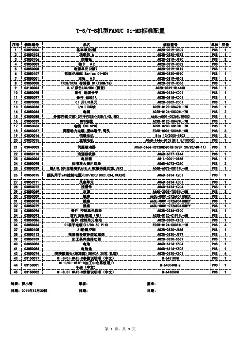
发那科标准配置
国家工程实验室NI PCI-651x系列产品手册说明书

Manufacturer: National InstrumentsBoard Assembly Part Numbers (Refer to Procedure 1 for identification procedure): Part Number and Revision Description191649A-01(L) or later PCI-6510190184A-01(L) or later PCI-6511190359A-01(L) or later PXI-6511190356A-02(L) or later PCI-6512190853A-02(L) or later PXI-6512190356A-01(L) or later PCI-6513190853A-01(L) or later PXI-6513189924A-02(L) or later PCI-6514190318A-02(L) or later PXI-6514189924A-01(L) or later PCI-6515190318A-01(L) or later PXI-6515191649A-02(L) or later PCI-6516191649A-03(L) or later PCI-6517191649A-04(L) or later PCI-6518191649A-05(L) or later PCI-6519192323A-01(L) or later PCI-6520192323A-02(L) or later PCI-6521192320A-01(L) or later PXI-6521Volatile MemoryTarget Data Type Size Backup1Accessible Accessible ProcedureEPM7032AEGlue Logic FPGA IntelEP1C3No No No Cycle Power Non-Volatile Memory (incl. Media Storage)Target Data Type Size BatteryBackupUserAccessibleSystemAccessibleSanitizationProcedureDevice configuration •Device information •FPGA bitstream •Output power-up states (except 6510/11) Flash 128 kB NoNoNoNoYesYesYesNoneNoneNone1 Refer to Terms and Definitions section for clarification of User and System AccessibleProceduresProcedure 1 – Board Assembly Part Number identification:To determine the Board Assembly Part Number and Revision, refer to the “P/N” label applied to the surface of your product as shown below. The Assembly Part Number should be formatted as “P/N: ######a-vvL” where “a” is the letter revision of the Board Assembly (eg. A, B, C…) and the “vv” is the type identifier. If the product is RoHS compliant, “L” can be found at the end of the part number.PCI-6510/16/17/18/19PCI-6511 PXI-6511PCI-6512/13 PXI-6512/13PCI-6514/15PXI-6514/15PCI-6520/21 (Bottom View)PXI-6521Terms and DefinitionsCycle Power:The process of completely removing power from the device and its components and allowing for adequate discharge. This process includes a complete shutdown of the PC and/or chassis containing the device; a reboot is not sufficient for the completion of this process.Volatile Memory:Requires power to maintain the stored information. When power is removed from this memory, its contents are lost. This type of memory typically contains application specific data such as capture waveforms.Non-Volatile Memory:Power is not required to maintain the stored information. Device retains its contents when power is removed.This type of memory typically contains information necessary to boot, configure, or calibrate the product or may include device power up states.User Accessible:The component is read and/or write addressable such that a user can store arbitrary information to the component from the host using a publicly distributed NI tool, such as a Driver API, the System Configuration API, or MAX. System Accessible:The component is read and/or write addressable from the host without the need to physically alter the product. Clearing:Per NIST Special Publication 800-88 Revision 1, “clearing” is a logical technique to sanitize data in all User Accessible storage locations for protection against simple non-invasive data recovery techniques using the same interface available to the user; typically applied through the standard read and write commands to the storage device.Sanitization:Per NIST Special Publication 800-88 Revision 1, “sanitization” is a process to render access to “Target Data” on the media infeasible for a given level of effort. In this document, clearing is the degree of sanitization described.。
芯片24C64中文资料

芯片24C64中文资料I2C总线I2C总线(Inter Integrated Circuit内部集成电路总线)是两线式串行总线,仅需要时钟和数据两根线就能够进行数据传输,仅需要占用微处理器的2个IO引脚,使用时十分方便。
I2C总线还能够在同一总线上挂多个器件,每个器件能够有自己的器件地址,读写操作时需要先发送器件地址,该地址的器件得到确认后便执行相应的操作,而在同一总线上的其它器件不做响应,称之为器件寻址,那个原理就像我们打的原理相当。
I2C总线产生80年代,由PHLIPS公司开发,早期多用于音频和视频设备,现在I2C总线的器件和设备已多不胜数。
最常见的采纳I2C总线的EEPROM也已被广泛使用于各种家电、工业及通信设备中,要紧用于储存设备所需要的配置数据、采集数据及程序等。
生产I2C总线EEPROM的厂商专门多,如ATMEL、Microchip公司,它们差不多上以24来开头命名芯片型号,最常用确实是24C系列。
24C系列从24C01到24C512,C后面的数字代表该型号的芯片有多少K 的储备位。
如ATMEL的24C64,储备位是64K位,也确实是说能够储备8K(8192)字节,它支持1.8V到5V电源,能够擦写1百万次,数据能够保持100年,使用5V电源时时钟能够达到400KHz,同时有多种封装可供选择。
我们能够专门容易的在周围的电器设备中发觉它们的身影,如电视中用于储存频道信息,电脑内存条中储存内存大小等相关信息,汽车里用于储存里程信息等等。
图一确实是ATMEL24C64芯片的PID封装和用于内存条SPD(Serial Presence Detect)上的24芯片。
图1图2图二是ATMEL公司24C64的引脚定义图。
A0-A2用于设置芯片的器件地址,在同一总线上有多个器件时,能够通过设置A0-A2引脚来确定器件地址。
SDA是串行数据引脚,用于在芯片读写时输入或输出数据、地址等,那个引脚是双向引脚,它是漏极开路的,使用时需要加上一个上拉电阻。
HCPL-0601中文资料

HCPL-0601中⽂资料CAUTION: The small device geometries inherent to the design of this bipolar component increase the component's susceptibility to damage from electrostatic discharge (ESD). It is advised that normal static precautions be taken in handling and assembly of this component to prevent damage and/or degradation which may be induced by ESD.Small Outline, 5 Lead, High CMR, High Speed, Logic Gate Optocouplers Technical DataHCPL-M600HCPL-M601HCPL-M611DescriptionThese small outline high CMR,high speed, logic gate optocoup-lers are single channel devices in a five lead miniature footprint.They are electrically equivalent to the following Agilentoptocouplers (except there is no output enable feature):SO-5 Package Standard DIP SO-8 Package HCPL-M6006N137HCPL-0600HCPL-M601HCPL-2601HCPL-0601HCPL-M611HCPL-2611HCPL-0611The SO-5 JEDEC registered (MO-155) package outline does not require “through holes” in a PCB.This package occupies approximately one fourth the footprint area of the standard dual-in-line package. The lead profile is designed to be com-patible with standard surface mount processes.The HCPL-M600/01/11 optically coupled gates combine a GaAsP light emitting diode and an integrated high gain photon detector. The output of thedetector I.C. is an Open-collectorSchottky-clamped transistor. The internal shield provides a guaranteed common modetransient immunity specification of 5,000 V/µs for the HCPL-M601,and 10,000 V/µs for the HCPL-M611.This unique design provides maximum ac and dc circuit isolation while achieving TTL compatibility. The optocoupler ac and dc operational parameters are guaranteed from -40°C to 85°C allowing trouble free system performance.FeaturesSurface MountableVery Small, Low Profile JEDEC Registered Package OutlineCompatible with Infrared Vapor Phase Reflow and Wave Soldering Processes Internal Shield for High Common Mode Rejection (CMR)HCPL-M601: 10,000 V/µs at V CM = 50 VHCPL-M611: 15,000 V/µs at V CM = 1000 VHigh Speed: 10 Mbd LSTTL/TTL Compatible Low Input Current Capability: 5 mAGuaranteed ac and dc Performance overTemperature: -40°C to 85°C ? Recognized under theComponent Program of U.L.(File No. E55361) forDielectric Withstand Proof Test Voltage of 2500 Vac, 1MinuteThe HCPL-M600/01/11 are suitable for high speed logic interfacing, input/outputbuffering, as line receivers in environments that conventionalline receivers cannot tolerate, and are recommended for use inextremely high ground or induced noise environments.Outline Drawing (JEDEC MO-155)ApplicationsIsolated Line Receiver Simplex/Multiplex Data TransmissionComputer-Peripheral InterfaceMicroprocessor System InterfaceDigital Isolation for A/D, D/A ConversionSwitching Power Supply Instrument Input/Output IsolationGround Loop Elimination Pulse Transformer ReplacementPin Location (for reference only)SchematicUSE OF A 0.1 µF BYPASS CAPACITOR MUST BE CONNECTED BETWEEN PINS 6 AND 4 (SEE NOTE 1). V CC V OGNDTRUTH TABLE (POSITIVE LOGIC)LEDONOFFOUTPUT L H65431V CCV OUT GNDANODE 0.71 (0.028)UNDERSIDE OF THE PACKAGEDIMENSIONS IN MILLIMETERS (INCHES) * MAXIMUM MOLD FLASH ON EACH SIDE IS 0.15 mm (0.006) Recommended Operating ConditionsParameterSymbol Min.Max.Units Input Current, Low Level I FL *0250µA Input Current, High Level I FH 515m A Supply Voltage, Output V CC 4.55.5V Fan Out (R L = 1 k ?)N 5TTLLoads Output Pull-Up Resistor R L 3304,000?Operating TemperatureT A-4085°C* The off condition can also be guaranteed by ensuring that V F (off) ≤ 0.8 volts.Absolute Maximum Ratings(No Derating Required up to 85°C)Storage Temperature....................................................-55°C to +125°C Operating Temperature ..................................................-40°C to +85°C Forward Input Current - I F (see Note 2).......................................20 mA Reverse Input Voltage - V R .................................................................5 V Supply Voltage - V CC (1 Minute Maximum)........................................7 V Output Collector Current - I O ........................................................50 mA Output Collector Power Dissipation .. (85)mW Output Collector Voltage - V O ............................................................7 V (Selection for higher output voltages up to 20 V is available)Infrared and Vapor Phase Reflow Temperature.......................see belowMaximum Solder Reflow Thermal Profile.(Note: Use of Non-Chlorine Activated Fluxes is Recommended.)240TIME – MINUTEST E M P E R A T U R E – °C220200180160140120100806040200260Insulation Related SpecificationsParameter Symbol Value Units ConditionsMin. External Air Gap L(IO1)≥5mm Measured from input terminals (Clearance)to output terminalsMin. External Tracking Path L(IO2)≥5mm Measured from input terminals (Creepage)to output terminalsMin. Internal Plastic Gap0.08mm Through insulation distance (Clearance)conductor to conductor Tracking Resistance CTI175V DIN IEC 112/VDE 0303 Part 1 Isolation Group (per DIN VDE 0109)IIIa Material Group DIN VDE 0109 Electrical SpecificationsOver recommended temperature (T A = -40°C to 85°C) unless otherwise specified. (See note 1.)*All typicals at T A = 25°C, V CC = 5 V.Switching SpecificationsOver recommended temperature (T A = -40°C to 85°C), V CC = 5 V, I F = 7.5 mA unless otherwise specified.*All typicals at T A = 25°C, V CC = 5 V.Notes:1. Bypassing of the power supply line is required with a 0.1 µF ceramic disc capacitor adjacent to each optocoupler. The total leadlength between both ends of the capacitor and the isolator pins should not exceed 10mm.2. Peaking circuits may produce transient input currents up to 50 mA, 50 ns maximum pulse width, provided average current does not exceed 20mA.3. Device considered a two terminal device: pins 1 and 3 shorted together, and pins 4, 5 and 6 shorted together.4. In accordance with UL 1577, each optocoupler is proof tested by applying an insulation test voltage ≥3000 V RMS for 1 second(Leakage detection current limit, I I-O≤ 5 µA).5. The t PLH propagation delay is measured from 3.75 mA point on the falling edge of the input pulse to the 1.5 V point on the rising edge of the output pulse.6. The t PHL propagation delay is measured from 3.75 mA point on the rising edge of the input pulse to the 1.5 V point on the falling edge of the output pulse.7. CM H is the maximum tolerable rate of rise of the common mode voltage to assure that the output will remain in a high logicstate (i.e., V OUT > 2.0V).8. CM L is the maximum tolerable rate of fall of the common mode voltage to assure that the output will remain in a low logic state (i.e., V OUT > 0.8 V).9. For sinusoidal voltages, (|dV CM|/dt)max = πf CM V CM(p-p).10. See application section; “Propagation Delay, Pulse-Width Distortion and Propagation Delay Skew” for more information.11. t PSK is equal to the worst case difference in t PHL and/or t PLH that will be seen between units at any given temperature withinthe worst case operating condition range.Figure 5. Low Level Output Current vs. Temperature.Figure 4. Output Voltage vs.Forward Input current.Figure 1. High Level Output Current vs. Temperature.Figure 2. Low Level Output Voltage vs. Temperature.Figure 3. Input Diode Forward Characteristic.Figure 6. Test Circuit for t PHL and t PLH .I O H – H I G H L E V E L O U T P U T C U R R E N T – µAT A – TEMPERATURE – °C101550.4T A – TEMPERATURE – °C 0.30.1V O L – L O W L E V E L O U T P U T V O L T A G E – V0.2V F – FORWARD VOLTAGE – VOLTS10I F – F O R W A R D C U R R E N T – m A100I F – FORWARD INPUT CURRENT – mAV O – O U T P U TV O L T A G E – VI O L – L O W L E V E L O U T P U T C U R R E N T – m A T A – TEMPERATURE – °C60802040OUTPUT V O MONITORING NODEI FV F = 7.5 mAF = 3.75 mAFigure 12. Temperature Coefficient for Forward Voltage vs. Input Current.Figure 10. Rise and Fall Time vs.Temperature.Figure 9. Pulse Width Distortion vs.Temperature.Figure 8. Propagation Delay vs.Pulse Input Current.Figure 7. Propagation Delay vs.Temperature.Figure 11. Test Circuit for Common Mode Transient Immunity and Typical Waveforms.10080T A – TEMPERATURE – °C 600t P – P R O P A G A T I O N D E L A Y – n s402010590I F – PULSE INPUT CURRENT – mA7530t P – P R O P A G A T I O N D E L A Y – n s60454030T A – TEMPERATURE – °C20P W D – P U L S E W I D T H D I S T O R T I O N – n s10-10t r , t f– R I S E , F A L L T I M E – n sT A – TEMPERATURE – °Cd V F /d T – F O R W A R D V O L T A G E T E M P E R A T U R E C O E F F I C I E N T – m V /°C0.1110100I F – PULSE INPUT CURRENT – mA-1.4-2.2-2.0-1.8-1.6-1.2-2.4V O 0.5 VV O (MIN.)5 V0 V SWITCH AT A: I F = 0 mA SWITCH AT B: I F = 7.5 mAV CMCM HCM LV O (MAX.)V CM (PEAK)V O+5 VO GENERATOR Z O = 50 ?Propagation Delay, Pulse-Width Distortion and Propagation Delay Skew Propagation delay is a figure of merit which describes how quickly a logic signal propagates through a system. The propaga-tion delay from low to high (t PLH) is the amount of time required for an input signal to propagate to the output, causing the output to change from low to high. Similarly, the propagation delay from high to low (t PHL) is the amount of time required for the input signal to propagate to the output, causing the output to change from high to low (see Figure 7).Pulse-width distortion (PWD) results when t PLH and t PHL d iffer in value. PWD is defined as the difference between t PLH and t PHL and often determines the maxi-mum data rate capability of a transmission system. PWD can be expressed in percent by dividing the PWD (in ns) by the minimum pulse width (in ns) being transmitted. Typically, PWD on the order of 20-30% of the minimum pulse width is tolerable; the exact figure depends on the particular application (RS232,RS422, T-1, etc.).Propagation delay skew, t PSK, is an important parameter to consider in parallel data appli-cations where synchronization of signals on parallel data lines is a concern. If the parallel data is being sent through a group ofoptocouplers, differences inpropagation delays will cause thedata to arrive at the outputs of theoptocouplers at different times. Ifthis difference in propagationdelays is large enough, it willdetermine the maximum rate atwhich parallel data can be sentthrough the optocouplers.Propagation delay skew is definedas the difference between theminimum and maximumpropagation delays, either t PLH ort PHL, for any given group ofoptocouplers which are operatingunder the same conditions (i.e.,the same drive current, supplyvoltage, output load, andoperating temperature). Asillustrated in Figure 15, if theinputs of a group of optocouplers are switched either ON or OFF at the same time, t PSK is the difference between the shortest propagation delay, either t PLH or t PHL, and the longest propagation delay, either t PLH or t PHL.As mentioned earlier, t PSK can determine the maximum parallel data transmission rate. Figure 11 is the timing diagram of a typical parallel data application with both the clock and the data lines being sent through optocouplers. The figure shows data and clock signals at the inputs and outputs of the optocouplers. To obtain the maximum data transmission rate, both edges of the clock signal are being used to clock the data; if only one edge were used, the clock signal would need to be twice as fast.Propagation delay skew represents the uncertainty of where an edge might be after being sent through an optocoupler. Figure 16 shows that there will be uncertainty in both the data and the clock lines. It is important that these two areas of uncertainty not overlap, otherwise the clock signal might arrive before all of the data outputs have settled, or some ofthe data outputs may start tochange before the clock signalhas arrived. From theseconsiderations, the absoluteminimum pulse width that can besent through optocouplers in aparallel application is twice t PSK. Acautious design should use aslightly longer pulse width toensure that any additionaluncertainty in the rest of thecircuit does not cause a problem.The t PSK specified optocouplersoffer the advantages ofguaranteed specifications forpropagation delays, pulse-widthdistortion and propagation delayskew over the recommendedtemperature, and input current,and power supply ranges.Figure 15. Illustration ofPropagation Delay Skew – t PSK .Figure 13. Input Threshold Current vs. Temperature.Figure 14. Recommended TTL/LSTTL to TTL/LSTTL Interface Circuit. Figure 16. Parallel Data Transmission Example.I T H – I N P U T T H R E S H O L D C U R R E N T – m AT A – TEMPERATURE – °C452316V* DIODE D1 (1N916 OR EQUIVALENT) IS NOT REQUIRED FOR UNITS WITH OPEN COLLECTOR OUTPUT. CC 2I FV OI FV ODATAINPUTS CLOCKDATAOUTPUTSCLOCK/doc/9b0bff6d783e0912a2162a2e.html Data subject to change.Copyright ? 1999 Agilent Technologies Obsoletes 5091-9635E (10/93)5966-4942E (11/99)。
25LC640中文翻译资料

25LC640中文翻译资料山东泰开自动化李凯设备选择表(25AA64025C640)64KSPI总线串口EEPROM:封装类型:方块图特征:低功率COMS工艺-写电流:3mA标准-读电流:500u标准-待机电流:500nA标准8192某8位组织32字节页写周期时间:5mA最大自动同步擦除和写入周期块写入保护-未保护,1/4,1/2,或全部数组内置的写保护-电源开/关数据保护电路-写允许锁存器-写保护管脚连续读高可靠性-耐久度:1M周期(可保证的)-数据保持:大于200年-静电防护:大于4000V8脚PDIP,SOPC,和TSSOP封装温度范围支持;-商业级:(C)0℃至+70℃-工业级:(I)-40℃至+85℃-汽车级:(E)-40℃至+125℃说明:美国微芯科技公司的25AA640/25LC640/25C640(25某某640)是64K 比特电可擦除PROM。
这个存储器的使用通道是简单串行外围接口(SPI)兼容串行总线。
这个总线信号需要时钟输入(SCK)加单独数据在(SI)和数据输出(SO)连线。
进入装置的控制是通过芯片选择(CS)输入。
通信到装置能够暂停通道保持管脚(HOLD)。
虽然装置是暂停,转变在输入将是忽略,除了志片的选择,允许主动服务较高优先级的中断。
1.0电气特性图形1-1:AC测试电路1.1最大等级Vcc.................................7.0V全部输入和输出w.r.t.V...-0.6至Vcc+1.0V储存温度.....................-65℃至150℃引线的焊接温度(10秒).............+300℃静电保护在全部管脚...................4kV注意:强调以上这些列出关于“最大等级”可能引出永久损伤到设备。
这强调的等级仅和设备的功能操作,而且那些或任何其它的条件超出那些声明在说明书的操作表中是未隐含的。
- 1、下载文档前请自行甄别文档内容的完整性,平台不提供额外的编辑、内容补充、找答案等附加服务。
- 2、"仅部分预览"的文档,不可在线预览部分如存在完整性等问题,可反馈申请退款(可完整预览的文档不适用该条件!)。
- 3、如文档侵犯您的权益,请联系客服反馈,我们会尽快为您处理(人工客服工作时间:9:00-18:30)。
1640120fTYPICAL APPLICATIONFEATURESAPPLICATIONSDESCRIPTIONDistortion Differential ADCDriver for 140MHz IFThe LTC ®6401-20 is a high-speed differential amplifi er targeted at processing signals from DC to 140MHz. The part has been specifi cally designed to drive 12-, 14- and 16-bit ADCs with low noise and low distortion, but can also be used as a general-purpose broadband gain block.The LTC6401-20 is easy to use, with minimal support circuitry required. The output common mode voltage is set using an external pin, independent of the inputs, which eliminates the need for transformers or AC-coupling ca-pacitors in many applications. The gain is internally fi xed at 20dB (10V/V).The LTC6401-20 saves space and power compared to alternative solutions using IF gain blocks and transform-ers. The LTC6401-20 is packaged in a compact 16-lead 3mm × 3mm QFN package and operates over the –40°C to 85°C temperature range.■1.3GHz –3dB Bandwidth ■ Fixed Gain of 10V/V (20dB)■ –93dBc IMD 3 at 70MHz (Equivalent OIP 3 = 50.5dBm)■ –74dBc IMD 3 at 140MHz (Equivalent OIP 3 = 41dBm)■ 1nV/√H z Internal Op Amp Noise ■2.1nV/√H z Total Input Noise ■ 6.2dB Noise Figure■ Differential Inputs and Outputs ■ 200Ω Input Impedance■ 2.85V to 3.5V Supply Voltage ■ 50mA Supply Current (150mW)■ 1V to 1.6V Output Common Mode Voltage, Adjustable■ DC- or AC-Coupled Operation■Max Differential Output Swing 4.4V P-P■ Small 16-Lead 3mm × 3mm × 0.75mm QFN Package■Differential ADC Driver ■ Differential Driver/Receiver■ Single Ended to Differential Conversion ■ IF Sampling Receivers ■ SAW Filter InterfacingSingle-Ended to Differential ADC DriverEquivalent Output IP3 vs FrequencyFREQUENCY (MHz)0O U T P U T I P 3 (d B m )70(NOTE 7)605040302010010050150640120 TA01b200LTC6401-202640120fABSOLUTE MAXIMUM RATINGSSupply Voltage (V + – V –) ..........................................3.6V Input Current (Note 2) ..........................................±10mA Operating Temperature Range(Note 3) ...............................................–40°C to 85°C Specifi ed Temperature Range(Note 4) ...............................................–40°C to 85°C Storage Temperature Range ...................–65°C to 150°C Maximum Junction Temperature...........................150°C(Note 1)161514135678TOP VIEW UD PACKAGE16-LEAD (3mm × 3mm) PLASTIC QFN 9101117124321V +V OCM V +V –V –ENABLE V +V ––I N–I N+I N +I N–O U T–O U T F+O U T F+O U TT JMAX = 150°C, θJA = 68°C/W, θJC = 4.2°C/WEXPOSED PAD (PIN 17) IS V –, MUST BE SOLDERED TO PCBORDER INFORMATIONLTC6400 AND LTC6401 SELECTOR GUIDEPART NUMBER GAIN(dB)GAIN (V/V)Z IN (DIFFERENTIAL)(Ω)I CC (mA)LTC6400-20201020090LTC6401-20201020050In addition to the LTC6401 family of amplifi ers, a lower distortion LTC6400 family is available. The LTC6400 is pin compatible to the LTC6401, and has the same low noise performance. The low distortion of the LTC6400 comes at the expense of higher power consumption. Please refer to the separate LTC6400 data sheets for complete details. Other gain versions from 8dB to 26dB will follow.Please check each datasheet for complete details.PIN CONFIGURATIONLEAD FREE FINISH TAPE AND REEL PART MARKING*PACKAGE DESCRIPTIONTEMPERATURE RANGE LTC6401CUD-20#PBF LTC6401CUD-20#TRPBF LCDB 16-Lead (3mm × 3mm) Plastic QFN 0°C to 70°C LTC6401IUD-20#PBFLTC6401IUD-20#TRPBFLCDB16-Lead (3mm × 3mm) Plastic QFN–40°C to 85°CConsult LTC Marketing for parts specifi ed with wider operating temperature ranges. *The temperature grade is identifi ed by a label on the shipping container.Consult LTC Marketing for information on non-standard lead based fi nish parts.For more information on lead free part marking, go to: /leadfree/ For more information on tape and reel specifi cations, go to: /tapeandreel/LTC6401-203640120fDC ELECTRICAL CHARACTERISTICS SYMBOL PARAMETER CONDITIONSMIN TYP MAX UNITS Input/Output CharacteristicG DIFF GainV IN = ±100mV Differential ●19.42020.6dB G TEMP Gain Temperature Drift V IN = ±100mV Differential●1mdB/°CV SWINGMIN Output Swing Low Each Output, V IN = ±400mV Differential ●90170mV V SWINGMAX Output Swing HighEach Output, V IN = ±400mV Differential ●2.3 2.44V V OUTDIFFMAX Maximum Differential Output Swing 1dB Compressed 4.4V P-P I OUT Output Current Drive Single-Ended ●10mAV OS Input Offset Voltage Differential ●–22mV TCV OS Input Offset Voltage DriftDifferential● 1.4μV/°CI VRMIN Input Common Mode Voltage Range, MIN 1V I VRMAX Input Common Mode Voltage Range, MAX 1.6V R INDIFF Input Resistance Differential●170200230ΩC INDIFF Input Capacitance Differential, Includes Parasitic 1pF R OUTDIFF Output Resistance Differential ●182532ΩR OUTFDIFF Filtered Output Resistance Differential●85100115ΩC OUTFDIFF Filtered Output Capacitance Differential, Includes Parasitic2.7pF CMRR Common Mode Rejection Ratio Input Common Mode Voltage 1.1V to 1.4V ●4566dB Output Common Mode Voltage ControlG CM Common Mode GainV OCM = 1V to 1.6V1V/VV OCMMIN Output Common Mode Range, MIN●11.1V V V OCMMAX Output Common Mode Range, MAX●1.61.5V V V OSCM Common Mode Offset Voltage V OCM = 1.1V to 1.5V●–1515mV TCV OSCM Common Mode Offset Voltage Drift ●6μV/°C IV OCM V OCM Input Current ●515μA E N A B L E Pin V IL E N A B L E Input Low Voltage ●0.8V V IH E N A B L E Input High Voltage ●2.4V I IL E N A B L E Input Low Current E N A B L E = 0.8V ●±0.5μA I IHE N A B L E Input High Current E N A B L E = 2.4V●1.23μA Power Supply V S Operating Supply Range ●2.8533.5V I S Supply CurrentE N A B L E = 0.8V ●385062mA I SHDN Shutdown Supply Current E N A B L E = 2.4V ●13mA PSRRPower Supply Rejection Ratio (Differential Outputs)2.85V to3.5V●5584dBThe ● denotes the specifi cations which apply over the full operatingtemperature range, otherwise specifi cations are at T A = 25°C. V + = 3V, V –= 0V, +IN = –IN = V OCM = 1.25V, E N A B L E = 0V, No R L unlessotherwise noted.LTC6401-204640120fAC ELECTRICAL CHARACTERISTICSSpecifi cations are at T A = 25°C. V + = 3V, V – = 0V, +IN and –INfl oating, V OCM = 1.25V, E N A B L E = 0V, No R L unless otherwise noted.SYMBOL PARAMETER CONDITIONS MINTYP MAXUNITS –3dBBW –3dB Bandwidth200mV P-P ,OUT (Note 6) 1.25GHz 0.1dBBW Bandwidth for 0.1dB Flatness 200mV P-P ,OUT (Note 6)130MHz 0.5dBBW Bandwidth for 0.5dB Flatness 200mV P-P ,OUT (Note 6)250MHz 1/f 1/f Noise Corner 12.5kHz SR Slew Rate Differential (Note 6)4500V/μs t S1%1% Settling Time2V P-P ,OUT (Note 6)2ns t OVDR Output Overdrive Recovery Time 1.9V P-P ,OUT (Note 6)7ns t ON Turn-On Time +OUT, –OUT Within 10% of Final Values 78ns t OFF Turn-Off TimeI CC Falls to 10% of Nominal146ns –3dBBW CMCommon Mode Small Signal –3dB BW0.1V P-P at V OCM , Measured Single-Ended at Output (Note 6)15MHz10MHz Input Signal HD 2,10M /HD 3,10MSecond/Third Order HarmonicDistortion2V P-P ,OUT , R L = 400Ω–122/–92dBc 2V P-P ,OUT , No R L –110/–103dBc 2V P-P ,OUTFILT , No R L–113/–102dBc IMD 3,10MThird-Order Intermodulation (f1 = 9.5MHz f2 = 10.5MHz)2V P-P ,OUT Composite, R L = 400Ω–96dBc 2V P-P ,OUT Composite, No R L –108dBc 2V P-P ,OUTFILT Composite, No R L–105dBc OIP 3,10M Third-Order Output Intercept Point (f1 = 9.5MHz f2 = 10.5MHz)2V P-P ,OUT Composite, No R L (Note 7)58dBm P 1dB,10M 1dB Compression Point R L = 375Ω (Notes 5, 7)17.3dBm NF 10M Noise FigureR L = 375Ω (Note 5)6.2dB e IN,10M Input Referred Voltage Noise DensityIncludes Resistors (Short Inputs)2.1nV/√H z e ON,10MOutput Referred Voltage Noise Density Includes Resistors (Short Inputs)21nV/√H z70MHz Input Signal HD 2,70M /HD 3,70MSecond/Third Order Harmonic Distortion2V P-P ,OUT , R L = 400Ω–91/–80dBc 2V P-P ,OUT , No R L –95/–88dBc 2V P-P ,OUTFILT , No R L–95/–88dBc IMD 3,70MThird-Order Intermodulation (f1 = 69.5MHz f2 = 70.5MHz)2V P-P ,OUT Composite, R L = 400Ω–88dBc 2V P-P ,OUT Composite, No R L –93dBc 2V P-P ,OUTFILT Composite, No R L–92dBc OIP 3,70M Third-Order Output Intercept Point (f1 = 69.5MHz f2 = 70.5MHz)2V P-P ,OUT Composite, No R L (Note 7)50.5dBm P 1dB,70M 1dB Compression Point R L = 375Ω (Notes 5, 7)17.3dBm NF 70M Noise FigureR L = 375Ω (Note 5)6.1dB e IN,70M Input Referred Voltage Noise DensityIncludes Resistors (Short Inputs)2.1nV/√H z e ON,70MOutput Referred Voltage Noise Density Includes Resistors (Short Inputs)21nV/√H z140MHz Input SignalHD 2,140M /HD 3,140M Second/Third Order HarmonicDistortion2V P-P ,OUT , R L = 400Ω–80/–57dBc 2V P-P ,OUT , No R L –81/–60dBc 2V P-P ,OUTFILT , No R L–80/–65dBcLTC6401-205640120fAC ELECTRICAL CHARACTERISTICS FREQUENCY (MHz)P H A S E (D E G R E E )1000–100–200–300–400GROUP DELAY (ns)1.51.20.90.60.302004006008001000640120 G03FREQUENCY (MHz)101001000N O R M A L I Z E D G A I N (d B )1.00.8–0.80.6–0.60.4–0.40.2–0.20–1.0640120 G02FREQUENCY (MHz)1010010003000G A I N (d B )2520151050640120 G01Note 1: Stresses beyond those listed under Absolute Maximum Ratings may cause permanent damage to the device. Exposure to any Absolute Maximum Rating condition for extended periods may affect device reliability and lifetime.Note 2: Input pins (+IN, –IN) are protected by steering diodes to either supply. If the inputs go beyond either supply rail, the input current should be limited to less than 10mA.Note 3: The LTC6401C and LTC6401I are guaranteed functional over the operating temperature range of –40°C to 85°C.Note 4: The LTC6401C is guaranteed to meet specifi ed performance from 0°C to 70°C. It is designed, characterized and expected to meet specifi ed performance from –40°C to 85°C but is not tested or QA sampled at thesetemperatures. The LTC6401I is guaranteed to meet specifi ed performance from –40°C to 85°C.Note 5: Input and output baluns used. See Test Circuit A.Note 6: Measured using Test Circuit B.Note 7: Since the LTC6401-20 is a feedback amplifi er with low output impedance, a resistive load is not required when driving an AD converter. Therefore, typical output power is very small. In order to compare the LTC6401-20 with amplifi ers that require 50Ω output load, the LTC6401-20 output voltage swing driving a given R L is converted to OIP 3 and P 1dB as if it were driving a 50Ω load. Using this modifi ed convention, 2V P-P is by defi nition equal to 10dBm, regardless of the actual R L .TYPICAL PERFORMANCE CHARACTERISTICSFrequency ResponseGain 0.1dB FlatnessS21 Phase and Group Delay vs FrequencySYMBOL PARAMETERCONDITIONSMINTYP MAXUNITS IMD 3,140MThird-Order Intermodulation(f1 = 139.5MHz f2 = 140.5MHz)2V P-P ,OUT Composite, R L = 400Ω–71dBc 2V P-P ,OUT Composite, No R L –74dBc 2V P-P ,OUTFILT Composite, No R L –72dBc OIP 3,140M Third-Order Output Intercept Point(f1 = 139.5MHz f2 = 140.5MHz)2V P-P ,OUT Composite, No R L (Note 7)41dBm P 1dB,140M 1dB Compression Point R L = 375Ω (Notes 5, 7)18dBm NF 140M Noise FigureR L = 375Ω (Note 5)6.4dB e IN,140M Input Referred Voltage Noise DensityIncludes Resistors (Short Inputs)2.1nV/√H z e ON,140M Output Referred Voltage Noise Density Includes Resistors (Short Inputs)22nV/√H z IMD 3,130M/150MThird-Order Intermodulation (f1 = 130MHz f2 = 150MHz) Measure at 170MHz2V P-P ,OUT Composite, R L = 375Ω (Note 5)–61–69dBcSpecifi cations are at T A = 25°C. V + = 3V, V – = 0V, +IN and –INfl oating, V OCM = 1.25V, E N A B L E = 0V, No R L unless otherwise noted.LTC6401-206640120fTIME (ns)O U T P U T V O L T A G E (V )2.50.51.02.01.5050100150200640120 G10TIME (ns)S E T T L I N G (%)54321–4–3–2–1–50123546640120 G1105101520TIME (ns)O U T P U T V O L T A G E (V )2.50.51.02.01.5640120 G09TIME (ns)0O U T P U T V O L T A G E (V )1.351.201.251.301.155101520640120 G08FREQUENCY (MHz)10N O I S E F I G U R E (d B )1510241214680113513791INPUT REFERRED NOISE VOLTAGE (nV/√Hz)64201001000640120 G07FREQUENCY (MHz)1I M P E D A N C E M A G N I T U D E (Ω)2502001501005002251751257525IMPEDANCE PHASE (DEGREE)10080604020–80–60–40–200–100101001000640120 G05FREQUENCY (MHz)10S P A R A M E T E R S (d B )0–10–20–30–40–50–60–70–8010010003000640120 G04TYPICAL PERFORMANCE CHARACTERISTICSInput and Output Refl ection and Reverse Isolation vs FrequencyInput and Output Impedance vs FrequencyPSRR and CMRR vs FrequencyOverdrive Transient Response1% Settling Time for 2V Output StepNoise Figure and Input Referred Noise Voltage vs FrequencySmall Signal Transient ResponseLarge Signal Transient ResponseFREQUENCY (MHz)1P S R R , C M R R (d B )1009080706050403001020101001000640120 G06LTC6401-207640120fOUTPUT COMMON MODE VOLTAGE (V)1.01.1 1.2 1.3 1.41.5640120 G18D I S T O R T I O N (d B c )–40–50–60–80–90–70–100FREQUENCY (MHz)T H I R D O R D E R I M D (d B c )640120 G1750100150200–40–50–60–80–90–70–120–110–100–40–50–60–80–90–70–120–110–100050100150200FREQUENCY (MHz)H A R M O N I CD I S T O R T I O N (d B c )640120 G1650100150200–40–50–60–80–90–70–120–110–100FREQUENCY (MHz)H A R M O N I C D I S T O R T I O N (d B c )640120 G15640120 G13FREQUENCY (MHz)H A R M O N I C D I S T O R T I O N (d B c )–40–50–60–80–90–70–120–110–10005010015020050100150200–40–50–60–80–90–70–120–110–100FREQUENCY (MHz)T H I R D O R D E R I M D (d B c )640120 G14FREQUENCY (MHz)H A R M O N I C D I S T O R T I O N (d B c )640120 G1250100150200–40–50–60–80–90–70–120–110–100TYPICAL PERFORMANCE CHARACTERISTICSHarmonic Distortion (Unfi ltered) vs FrequencyHarmonic Distortion (Filtered) vs FrequencyThird Order Intermodulation Distortion vs FrequencyHarmonic Distortion (Unfi ltered) vs FrequencyHarmonic Distortion (Filtered) vs FrequencyThird Order Intermodulation Distortion vs FrequencyHarmonic Distortion vs OutputCommon Mode Voltage (Unfi ltered Outputs)Equivalent Output 1dBCompression Point vs FrequencyFREQUENCY (MHz)50O U T P U T 1d B C O M P R E S S I O N (d B m )20191816171580110140170200640020 G19LTC6401-208640120fTIME (ns)–1000V O L T A G E (V )3.52.02.51.01.53.0–0.50.5100200300400500640120 G22SUPPLY CURRENT (mA)704060–1020305010TIME (ns)–100V O L T A G E (V )3.52.02.51.01.53.0–0.50.50100200300400500640120 G21SUPPLY CURRENT (mA)704060–102030501050100150200FREQUENCY (MHz)640120 G20O U T P U T I P 3 (d B m )706050402010300TYPICAL PERFORMANCE CHARACTERISTICSEquivalent Output Third Order Intercept vs FrequencyTurn-On TimeTurn-Off TimeLTC6401-209640120fBLOCK DIAGRAMPIN FUNCTIONSV + (Pins 1, 3, 10): Positive Power Supply (Normally tied to 3V or 3.3V). All three pins must be tied to the same voltage. Bypass each pin with 1000pF and 0.1μF capaci-tors as close to the pins as possible.V OCM (Pin 2): This pin sets the output common mode voltage. A 0.1μF external bypass capacitor is recom-mended.V – (Pins 4, 9, 12, 17): Negative Power Supply. All four pins must be connected to the same voltage/ground.–OUT, +OUT (Pins 5, 8): Unfi ltered Outputs. These pins have 12.5Ω series resistors.–OUTF, +OUTF (Pins 6, 7): F iltered Outputs. These pins have 50Ω series resistors and a 1.7pF shunt capacitance.E N A B L E (Pin 11): This pin is a logic input referenced to V –. If low, the part is enabled. If high, the part is disabled and draws approximately 1mA supply current. +IN (Pins 13, 14): Positive Input. Pins 13 and 14 are internally shorted together.–IN (Pins 15, 16): Negative Input. Pins 15 and 16 are internally shorted together.Exposed Pad (Pin 17): V –. The Exposed Pad must be con-nected to the same voltage/ground as pins 4, 9, 12.ENABLELTC6401-2010640120fAPPLICATIONS INFORMATIONCircuit OperationThe LTC6401-20 is a low noise and low distortion fully differential op amp/ADC driver with:• Operation from DC to 1.3GHz –3dB bandwidth impedance • Fixed gain of 10V/V (20dB) • Differential input impedance 200Ω • Differential output impedance 25Ω • Differential impedance of output fi lter 100ΩThe LTC6401-20 is composed of a fully differential amplifi er with on chip feedback and output common mode voltage control circuitry. Differential gain and input impedance are set by 100Ω/1000Ω resistors in the feedback network. Small output resistors of 12.5Ω improve the circuit stability over various load conditions. They also provide a possible external fi ltering option, which is often desirable when the load is an ADC.Filter resistors of 50Ω are available for additional fi ltering. Lowpass/bandpass fi lters are easily implemented with just a couple of external components. Moreover, they offer single-ended 50Ω matching in wideband applications and no external resistor is needed.The LTC6401-20 is very fl exible in terms of I/O coupling. It can be AC- or DC-coupled at the inputs, the outputs or both. Due to the internal connection between input and output, users are advised to keep input common mode voltage between 1V and 1.6V for proper operation. If the inputs are AC-coupled, the input common mode voltage is automatically biased close to V OCM and thus no external circuitry is needed for bias. The LTC6401-20 provides an output common mode voltage set by V OCM , which allows driving an ADC directly without external components such as a transformer or AC coupling capacitors. The input signal can be either single-ended or differential with only minor differences in distortion performance.Input Impedance and MatchingThe differential input impedance of the LTC6401-20 is 200Ω. If a 200Ω source impedance is unavailable, thenthe differential inputs may need to be terminated to a lower value impedance, e.g. 50Ω, in order to provide an imped-ance match to the source. Several choices are available. One approach is to use a differential shunt resistor (Figure 1). Another approach is to employ a wideband transformer (Figure 2). Both methods provide a wideband match. The termination resistor or the transformer must be placed close to the input pins in order to minimize the refl ection due to input mismatch. Alternatively, one could apply a narrowband impedance match at the inputs of the LTC6401-20 for frequency selection and/or noise reduction.Referring to F igure 3, LTC6401-20 can be easily confi gured for single-ended input and differential output without a balun. The signal is fed to one of the inputs through a matching network while the other input is connected to the same matching network and a source resistor. Because the return ratios of the two feedback paths are equal, theFigure 1. Input Termination for Differential 50Ω Input Impedance Using Shunt ResistorFigure 2. Input Termination for Differential 50Ω Input Impedance Using a 1:4 BalunLTC6401-2011640120ftwo outputs have the same gain and thus symmetrical swing. In general, the single-ended input impedance and termination resistor R T are determined by the combination of R S , R G and R F . For example, when R S is 50Ω, it is found that the single-ended input impedance is 200Ω and R T is 66.5Ω in order to match to a 50Ω source impedance.The LTC6401-20 is unconditionally stable. However, the overall differential gain is affected by both source imped-ance and load impedance as shown in Figure 4:A V V R R R V OUT IN S L L==++200020025•The noise performance of the LTC6401-20 also depends upon the source impedance and termination. For example, an input 1:4 balun transformer in Figure 2 improves SNR by adding 6dB of gain at the inputs. A trade-off between gain and noise is obvious when constant noise fi gure circle and constant gain circle are plotted within the sameFigure 4. Calculate Differential Gaininput Smith Chart, based on which users can choose the optimal source impedance for a given gain and noise requirement.Output Match and FilterThe LTC6401-20 can drive an ADC directly without external output impedance matching. Alternatively, the differential output impedance of 25Ω can be matched to higher value impedance, e.g. 50Ω, by series resistors or an LC network.The internal low pass fi lter outputs at +OUTF /–OUTF have a –3dB bandwidth of 590MHz. External capacitor can reduce the low pass fi lter bandwidth as shown in F igure 5. A bandpass fi lter is easily implemented with only a few components as shown in F igure 6. Three 39pF capacitors and a 16nH inductor create a bandpass fi lter with 165MHz center frequency, –3dB frequencies at 138MHz and 200MHz.APPLICATIONS INFORMATIONFigure 3. Input Termination for Single-Ended 50Ω Input ImpedanceFigure 5. LTC6401-20 Internal Filter Topology Modifi ed for Low Filter Bandwidth (Three External Capacitors)Figure 6. LTC6401-20 Application Circuit for Bandpass Filtering (Three External Capacitors, One External Inductor)LTC6401-2012640120fOutput Common Mode AdjustmentThe LTC6401-20’s output common mode voltage is set by the V OCM pin, which is a high impedance input. The output common mode voltage is capable of tracking V OCM in a range from 1V to 1.6V. Bandwidth of V OCM control is typically 15MHz, which is dominated by a low pass fi lter connected to the V OCM pin and is aimed to reduce com-mon mode noise generation at the outputs. The internal common mode feedback loop has a –3dB bandwidth around 300MHz, allowing fast common mode rejection at the outputs of the LTC6401-20. The V OCM pin should be tied to a DC bias voltage where a 0.1μF bypass capacitor is recommended. When interfacing with A/D converters such as the LT22xx families, the V OCM can be normally connected to the V CM pin of the ADC.Driving A/D ConvertersThe LTC6401-20 has been specifi cally designed to inter-face directly with high speed A/D converters. In Figure 7, an example schematic shows the LTC6401-20 with a single-ended input driving the LTC2208, which is a 16-bit, 130Msps ADC. Two external 10Ω resistors help eliminate potential resonance associated with stray capacitance of PCB traces and bond wire inductance of either the ADC input or the driver output. V OCM of the LTC6401-20 is connected to V CM of the LTC2208 at 1.25V. Alternatively, a single-ended input signal can be converted to differential signal via a balun and fed to the input of the LTC6401-20. The balun also converts input impedance to match 50Ω source impedance.Figure 7. Single-Ended Input to LTC6401-20 and LTC2208APPLICATIONS INFORMATIONTest CircuitsDue to the fully-differential design of the LTC6401 and its usefulness in applications with differing characteristic specifi cations, two test circuits are used to generate the information in this datasheet. Test Circuit A is DC987B, a two-port demonstration circuit for the LTC6401 family. The schematic and silkscreen are shown below. This circuit includes input and output transformers (baluns) for single-ended-to-differential conversion and imped-ance transformation, allowing direct hook-up to a 2-port network analyzer. There are also series resistors at the output to present the LTC6401 with a 375Ω differential load, optimizing distortion performance. Due to the input and output transformers, the –3dB bandwidth is reduced from 1.3GHz to approximately 1.1GHz.Test Circuit B uses a 4-port network analyzer to measure S-parameters and gain/phase response. This removes the effects of the wideband baluns and associated circuitry, for a true picture of the >1GHz S-parameters and AC characteristics.LTC6401-20 APPLICATIONS INFORMATIONTop Silkscreen13640120fLTC6401-2014640120fVERSIONICR3R4T1SL1SL2SL3-GLTC6401CUD-20OPEN OPENMINI-CIRCUITS TCM4-19 (1:4)6dB20dB14dB640120 TA03J5–OUTSL3(2)J4+OUT TP2V CC2.85V TO3.5VμFTP5V OCMJ7TEST OUTNOTE: UNLESS OTHERWISE SPECIFIED.(1) DO NOT STUFF.(2)SL = SIGNAL LEVELTP3GNDTYPICAL APPLICATIONDemo Circuit 987B Schematic (Test Circuit A)LTC6401-2015640120fInformation furnished by Linear Technology Corporation is believed to be accurate and reliable. However, no responsibility is assumed for its use. Linear Technology Corporation makes no representa-tion that the interconnection of its circuits as described herein will not infringe on existing patent rights.PACKAGE DESCRIPTIONRECOMMENDED SOLDER PAD PITCH AND DIMENSIONSNOTE:1. DRAWING CONFORMS TO JEDEC PACKAGE OUTLINE MO-220 VARIATION (WEED-2)2. DRAWING NOT TO SCALE3. ALL DIMENSIONS ARE IN MILLIMETERS4. DIMENSIONS OF EXPOSED PAD ON BOTTOM OF PACKAGE DO NOT INCLUDEMOLD FLASH. MOLD FLASH, IF PRESENT, SHALL NOT EXCEED 0.15mm ON ANY SIDE 5. EXPOSED PAD SHALL BE SOLDER PLATED6. SHADED AREA IS ONLY A REFERENCE FOR PIN 1 LOCATION ON THE TOP AND BOTTOM OF PACKAGEBOTTOM VIEW—EXPOSED PAD× 45° CHAMFERUD Package16-Lead Plastic QFN (3mm × 3mm)(Reference LTC DWG # 05-08-1691)TYPICAL APPLICATIONTest Circuit B, 4-Port Analysis+LTC6401-2016640120fLinear Technology Corporation1630 McCarthy Blvd., Milpitas, CA 95035-7417(408) 432-1900 ● FAX: (408) 434-0507 ● © LINEAR TECHNOLOGY CORPORA TION 2007LT 0907 • PRINTED IN USARELATED PARTSPART NUMBER DESCRIPTIONCOMMENTSHigh-Speed Differential Amplifi ers/Differential Op AmpsLT1993-2800MHz Differential Amplifi er/ADC Driver A V = 2V/V, OIP3 = 38dBm at 70MHz LT1993-4900MHz Differential Amplifi er/ADC Driver A V = 4V/V, OIP3 = 40dBm at 70MHz LT1993-10700MHz Differential Amplifi er/ADC Driver A V = 10V/V, OIP3 = 40dBm at 70MHzLT1994Low Noise, Low Distortion Differential Op Amp 16-Bit SNR and SFDR at 1MHz, Rail-to-Rail OutputsLT5514Ultralow Distortion IF Amplifi er/ADC Driver with Digitally Controlled GainOIP3 = 47dBm at 100MHz, Gain Control Range 10.5dB to 33dB LT5524Low Distortion IF Amplifi er/ADC Driver with Digitally Controlled GainOIP3 = 40dBm at 100MHz, Gain Control Range 4.5dB to 37dB LTC6400-20 1.8GHz Low Noise, Low Distortion, Differential ADC Driver A V = 20dB, 90mA Supply Current, IMD 3 = –65dBc at 300MHz LT6402-6300MHz Differential Amplifi er/ADC Driver A V = 6dB, Distortion < –80dBc at 25MHz LT6402-12300MHz Differential Amplifi er/ADC Driver A V = 12dB, Distortion < –80dBc at 25MHz LT6402-20300MHz Differential Amplifi er/ADC Driver A V = 20dB, Distortion < –80dBc at 25MHzLTC64063GHz Rail-to-Rail Input Differential Op Amp1.6nV/√Hz Noise, –72dBc Distortion at 50MHz, 18mALT6411Low Power Differential ADC Driver/Dual Selectable Gain Amplifi er16mA Supply Current, IMD3 = –83dBc at 70MHz, A V = 1, –1 or 2High-Speed Single-Ended Output Op AmpsLT1812/LT1813/LT1814High Slew Rate Low Cost Single/Dual/Quad Op Amps8nV/√Hz Noise, 750V/μs, 3mA Supply Current LT1815/LT1816/LT1817Very High Slew Rate Low Cost Single/Dual/Quad Op Amps 6nV/√Hz Noise, 1500V/μs, 6.5mA Supply Current LT1818/LT1819Ultra High Slew Rate Low Cost Single/Dual Op Amps 6nV/√Hz Noise, 2500V/μs, 9mA Supply CurrentLT6200/LT6201Rail-to-Rail Input and Output Low Noise Single/Dual Op Amps0.95nV/√Hz Noise, 165MHz GBW, Distortion = –80dBc at 1MHz LT6202/LT6203/LT6204Rail-to-Rail Input and Output Low Noise Single/Dual/Quad Op Amps 1.9nV/√Hz Noise, 3mA Supply Current, 100MHz GBW LT6230/LT6231/LT6232Rail-to-Rail Output Low Noise Single/Dual/Quad Op Amps 1.1nV/√Hz Noise, 3.5mA Supply Current, 215MHz GBW LT6233/LT6234/LT6235Rail-to-Rail Output Low Noise Single/Dual/Quad Op Amps 1.9nV/√Hz Noise, 1.2mA Supply Current, 60MHz GBWIntegrated Filters LTC1562-2Very Low Noise, 8th Order Filter Building Block Lowpass and Bandpass Filters up to 300kHz LT1568Very Low Noise, 4th Order Filter Building Block Lowpass and Bandpass Filters up to 10MHz LTC1569-7Linear Phase, Tunable 10th Order Lowpass Filter Single-Resistor Programmable Cut-Off to 300kHz LT6600-2.5Very Low Noise Differential 2.5MHz Lowpass Filter SNR = 86dB at 3V Supply, 4th Order Filter LT6600-5Very Low Noise Differential 5MHz Lowpass Filter SNR = 82dB at 3V Supply, 4th Order Filter LT6600-10Very Low Noise Differential 10MHz Lowpass Filter SNR = 82dB at 3V Supply, 4th Order Filter LT6600-15Very Low Noise Differential 15MHz Lowpass Filter SNR = 76dB at 3V Supply, 4th Order Filter LT6600-20Very Low Noise Differential 20MHz Lowpass FilterSNR = 76dB at 3V Supply, 4th Order Filter。