DS-LPC1778核心板用户手册V1.1
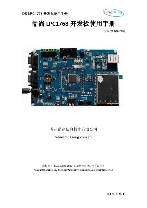
鼎尚 LPC1768 开发板使用手册
串行接口 以太网 MAC 带 RMII 接口和相关的 DMA 控制器; USB 2.0 全速从机/主机/OTG 控制器,带有用于从机、主机功能的片
内 PHY 和相关的 DMA 控制器; 4 个 UART、带小数波特率发生功能、内部 FIFO、DMA 支持和 RS-485
支持。1 个 UART 带有 modem 控制 IO 并支持 RS-485,全部的 UART 都支持 IrDA; CAN 控制器,带有 2 个通道; SPI 控制器,具有同步、串行、全双工通信和可编程的数据长度; 2 个 SSP 控制器,带有 FIFO,可按多种协议进行通信。其中一个可 选择用于 SPI,并且和 SPI 公用中断。SSP 接口可以与 GPDMA 控制器 一起使用。 3 个增强型的 IIC 总线接口。 IIS 接口,用于数字音频输入和输出,具有小数速率控制功能。
1. lpc1768-1_1_led_blinky..........................................................................................13 2. lpc1768-1_2_led_systick.........................................................................................16 3. lpc1768-1_3_led_os................................................................................................17 4. lpc1768-2_1_uart_echo..........................................................................................18 5. lpc1768-2_2_uart_shell ..........................................................................................19 6. lpc1768-2_3_uart_rs485.........................................................................................22 7. lpc1768-3_1_key_scan............................................................................................24 8. lpc1768-4_1_can.....................................................................................................25 9. lpc1768-5_1_i2c ......................................................................................................25 10. lpc1768-6_1_sd_fat ............................................................................................26 11. lpc1768-7_1_ad_da.............................................................................................27 12. lpc1768-8_1_USB_hid.........................................................................................27 13. lpc1768-8_2_USB_cdc.........................................................................................28 14. lpc1768-8_3_ USB _msc......................................................................................30 15. lpc1768-8_4_ USB_host......................................................................................31 16. lpc1768-9_1_eth_ping ........................................................................................32 17. lpc1768- 9_2_eth_stack......................................................................................33 18. lpc1768- 10_1_lcd_photo ...................................................................................37 19. lpc1768- 10_2_lcd_touch....................................................................................38 20. lpc1768- 11_1_flash_spi .....................................................................................38 21. lpc1768- 12_1_rtc ...............................................................................................38 22. lpc1768- 13_1_watchDog ...................................................................................40
路虎LPC17XX开发板使用手册
引脚定义如下:
引脚 信号描述 对应IO 引脚信号描述对应IO引脚信号描述对应IO
1 3V3 电源 2 GND 地 3 DB00
4 DB01 5 DB02 6 DB03
7 DB04 8 DB05 9 DB06
10 DB07 11 DB08 12 DB09
13 DB10 14 DB11 15 DB12
1 485A 2 485B
3 4
3.3 RS232通信接口COM1、COM2定义
RS232 connector COM1、COM2 (front view)
COM1定义
Pin number Description Pin number Description
1 NC 6 NC
丰富的板载资源:
1、2路 RS232串行接口(使用直通串口线、其中一路串口支持 ISP下载程序)
2、2路 CAN总线通信接口(CAN收发器:SN65VHD230)
3、RS485通信接口(485收发器:SP3485)
4、RJ45-10/100M Ethernet网络接口(以太网 PHY:DP83848)
10、IIC接口(24LC02)
11、SPI串行 FLASH接口(AT45DB161D)
12、2个用户按键,2个功能按键 Reset和 INT0按键,8个 LED灯
13、1个五向输入摇杆按键(Joystick)
14、串口 ISP下载功能(无需设置跳线),标准 JTAG下载、仿真调试接口。
Pin number Description Pin number Description
1 5V 4 CAN2H
2 CAN1H 5 CAN2L
ICP DAS WinCon8000 Series 硬件用户手册说明书

• WinCon 8000 Series
The WinCon 8000 is the flagship compact embedded controller manufactured by ICP DAS. Its leading technology gives you all of the best features of both traditional PLCs and Windows capable PCs. The WinCon 8000 system is powered by Windows and brings Windows programming style and skill into the world of PC-based PLCs. Application developers can directly develop their own programs in Microsoft’s Visual Studio .NET and Embedded Visual tools with the WinCon SDK, and then download them into WinCon 8000 for use. Or, they can port their favorite SCADA software onto WinCon 8000 for even easier application development. For SCADA applications, we also provide a product model embedded with InduSoft Web Studio run-time version to meet this need.
创龙SOM-TL5728F 核心板规格书说明书

核心板规格书Revision HistoryDraft Date Revision No.Description 2020/08/10V1.5 1.更新产品订购型。
2020/06/11V1.41.更换封面。
2.完善电气特性。
3.完善机械尺寸参数。
4.更新产品订购型号。
5.优化软硬件参数。
6.删除附录A。
2018/09/07V1.3 1.修改电气特性参数。
2018/06/10V1.21.核心板更新为A2版。
2.内容勘误,修改部分参数说明。
2017/12/27V1.11.内容勘误。
2.修改电气特性参数。
2017/09/01V1.0 1.初始版本。
目录1核心板简介 (4)2典型应用领域 (5)3软硬件参数 (6)4开发资料 (11)5电气特性 (12)6机械尺寸 (12)7产品订购型号 (13)8技术服务 (14)9增值服务 (14)更多帮助 (15)1核心板简介创龙SOM-TL5728F是一款基于TI Sitara系列AM5728双核ARM Cortex-A15+浮点双核DSP C66x+Xilinx Artix-7FPGA处理器设计的高端异构多核工业级核心板。
核心板内部AM5728与Artix-7通过GPMC、I2C通信总线连接,并通过工业级高速B2B连接器引出千兆网口、PCIe、USB 3.0、SATA等接口。
核心板经过专业的PCB Layout和高低温测试验证,稳定可靠,可满足各种工业应用环境。
用户使用核心板进行二次开发时,仅需专注上层运用,降低了开发难度和时间成本,可快速进行产品方案评估与技术预研。
图1核心板正面图图2核心板背面图图3核心板斜视图图4核心板侧视图2典型应用领域✓运动控制✓测试测量✓机器视觉✓智能电力✓视频追踪✓定位导航3软硬件参数硬件框图图5核心板硬件框图图6AM572x处理器功能框图图7Artix-7特性硬件参数表1AM5728端硬件参数CPU CPU:TI Sitara AM57282x ARM Cortex-A15,主频1.5GHz2x DSP C66x,主频750MHz,支持浮点运算2x IPU(Image Processing Unit),每个IPU子系统含2个ARM Cortex-M4核心,共4个ARM Cortex-M4核心2x PRU-ICSS,每个PRU-ICSS子系统含2个PRU(Programmable Real-time Unit)核心,共4个PRU核心,支持EtherCAT等协议1x IVA-HD Video Codec,支持1路1080P60H.264视频硬件编解码2x SGX5443D GPU图形加速器1x GC3202D图形加速器ROM 4/8GByte eMMC32Kbit ATAES132A-SHEQ加密芯片RAM1/2GByte DDR32.5MByte On-Chip MemoryB2B Connector 2x180pin公座高速B2B连接器,2x180pin母座高速B2B连接器,间距0.5mm,合高5mm,共720pinLED 1x电源指示灯2x用户可编程指示灯Sensor1x TMP102AIDRLT温度传感器硬件资源3x VIP(Video Input Ports),支持10路1080P60视频输入1x TV OUTPUT,支持HDMI/DPI1080P603x LCD OUTPUT3x eHRPWM3x eCAP3x eQEP1x NMI1x PCIe Gen2,支持一个双通道端口,或两个单通道端口,每通道最高通信速率5GBaud1x USB2.01x USB3.02x10/100/1000M Ethernet3x MMC/SD/SDIO10x UART1x JTAG2x Watchdog1x SATA1x GPMC5x I2C2x DCAN8x McASP1x QSPI4x SPI备注:B2B、电源、指示灯等部分硬件资源,AM5728与Artix-7共用。
LPC-P1227开发板用户手册说明书

LPC-P1227LPC-P1227 development board USER’S MANUALInitial release, March 2012Designed by OLIMEX Ltd, 2011All boards produced by Olimex LTD are ROHS compliantOLIMEX© 2012LPC-P1227 User's ManualDisclaimer:© 2012 Olimex Ltd. Olimex®, logo and combinations thereof, are registered trademarks of Olimex Ltd. Other terms and product names may be trademarks of others.The information in this document is provided in connection with Olimex products. No license, express or implied or otherwise, to any intellectual property right is granted by this document or in connection with the sale of Olimex products.Neither the whole nor any part of the information contained in or the product described in this document may be adapted or reproduced in any material from except with the prior written permission of the copyright holder.The product described in this document is subject to continuous development and improvements.All particulars of the product and its use contained in this document are given by OLIMEX in good faith. However all warranties implied or expressed including but not limited to implied warranties of merchantability or fitness for purpose are excluded. This document is intended only to assist the reader in the use of the product. OLIMEX Ltd. shall not be liable for any loss or damage arising from the use of any information in this document or any error or omission in such information or any incorrect use of the product.Thank you for purchasing LPC-P1227 development board assembled byOLIMEX LTDOLIMEX© 2012LPC-P1227 User's ManualTable of ContentsCHAPTER 1 (5)OVERVIEW (5)1. Introduction to the chapter (5)1.1 Features (5)1.2 Organization (6)CHAPTER 2 (7)SETTING UP THE LPC-P1227 BOARD (7)2. Introduction to the chapter (7)2.1 Electrostatic warning (7)2.2 Requirements (7)2.3 Powering the board (7)2.4 Prebuilt software (8)CHAPTER 3 (9)LPC-P1227 BOARD DESCRIPTION (9)3. Introduction to the chapter (9)3.1 Layout (top view) (9)CHAPTER 4 (10)THE LPC1227FBD64 MICROCONTROLLER (10)4. Introduction to the chapter (10)4.1 The microcontroller (10)CONTROL CIRCUITY (12)5. Introduction to the chapter (12)5.1 Reset (12)5.2 Clocks (12)CHAPTER 6 (13)HARDWARE (13)6. Introduction to the chapter (13)6.1 PWR Connector (13)6.2 SWD1 connector (13)6.3 SWD2 Header (14)6.4 UEXT (14)6.5 Pads on the proto area (16)6.6 RS232 Null-modem connector (17)6.7 Jumper description (18)6.8 LCD Display (19)OLIMEX© 2012LPC-P1227 User's Manual6.9 Additional hardware components (19)CHAPTER 7 (20)MEMORY AND BLOCK DIAGRAM (20)7. Introduction to the chapter (20)7.1 Memory organization (21)CHAPTER 8 (22)SCHEMATICS (22)8. Introduction to the chapter (22)8.1 Eagle schematic (22)8.2 Physical dimensions (24)CHAPTER 9 (25)REVISION HISTORY (25)9. Introduction to the chapter (25)9.1 Document revision (25)9.2 Web page of your device (25)OLIMEX© 2012LPC-P1227 User's ManualCHAPTER 1OVERVIEW1. Introduction to the chapterThank you for choosing the LPC-P1227 development board from Olimex! This document provides a User’s Guide for the Olimex LPC-P1227 development board. As an overview, this chapter gives the scope of this document and lists the board’s features. The document’s organization is then detailed.The LPC-P1227 development board enables code development of applications running on the LPC1227 Cortex-M0 microcontroller, manufactured by NXP Semiconductors.1.1 Features•MCU: LPC1227 Cortex-M0, up to 45Mhz, 128 kB Flash, 8kB SRAM, 2 UARTs , SPI, I2C,10 bit ADC•RS232•Buzzer•NOKIA 3310 LCD•12 MHz crystal resonator•Power supply circuit•Power-on LED•Debug interface – SWD (Serial Wire Debug)•UEXT connector•Two user leds•Three user buttons•Reset button•Prototype area•FR-4, 1.5 mm, soldermask, component print•Dimensions:80x50mm (3.15 x 1.97")OLIMEX© 2012LPC-P1227 User's Manual 1.2 OrganizationEach section in this document covers a separate topic, organized as follow:–Chapter 1 is an overview of the board usage and features–Chapter 2 provides a guide for quickly setting up the board–Chapter 3 contains the general board diagram and layout–Chapter 4 describes the component that is the heart of the board: the LPC1227FBD64 microcontroller–Chapter 5 is an explanation of the control circuitry associated with the microcontroller to reset. Also shows the clocks on the board–Chapter 6 covers the connector pinout, peripherals and jumper description–Chapter 7 shows the processor diagram and memory map–Chapter 8 provides the schematics–Chapter 9 contains the revision historyOLIMEX© 2012LPC-P1227 User's ManualCHAPTER 2SETTING UP THE LPC-P1227 BOARD2. Introduction to the chapterThis section helps you set up the LPC-P1227 development board for the first time.Please consider first the electrostatic warning to avoid damaging the board, then discover the hardware and software required to operate the board.The procedure to power up the board is given, and a description of the default board behavior is detailed.2.1 Electrostatic warningLPC-P1227 is shipped in a protective anti-static package. The board must not be exposed to high electrostatic potentials. A grounding strap or similar protective device should be worn when handling the board. Avoid touching the component pins or any other metallic element.2.2 RequirementsIn order to set up and program the LPC-P1227, the following items are required:- A source of power – the board can be powered through the PWR jack or through the SWD-1 (SWD-2) interface- In order to program the board you will need a programmer that supports SWD (Serial Wire Debug) interfaceAlso, a host-based software toolchain is required in order to program/debug the LPC-P1227 board. There are also a number of ready IDEs available like IAR Embedded Workbench,Rowley CrossWorks, Code Composer Studio, etc.The only low cost Olimex option at the time writing this guide is available if you use Rowley's Crossworks IDE. You can get any of our ARM-USB debuggers + ARM-JTAG-SWD adapter. As of moment of writing this guide OpenOCD 0.5.0 doesn't support SWD flashing.2.3 Powering the board- Provide between 5V and 9V to the board's PWR jackOLIMEX© 2012LPC-P1227 User's ManualOR- Connect your SWD debugger2.4 Prebuilt softwareOn powering the board the PWR LED should turn on. LED1 and LED2 should start blinking alternatively. The LCD display shows 6 lines of text. You can connect the board to a PC via RS232 Null-modem interface. Then start your favourite terminal program at 115200, 8-N-1 and reset the board. A line with the statuses of 4 buttons (USER3, USER2, USER1, WAKE_UP) and ISP_E jumper appears. Press the buttons to see their state changing or change the jumper position. Pressing escape will disconnect the RS232.OLIMEX© 2012LPC-P1227 User's ManualCHAPTER 3LPC-P1227 BOARD DESCRIPTION3. Introduction to the chapterHere you get acquainted with the main parts of the board. Note the names used on the board differ from the names used to describe them. For the actual names check the LPC-P1227 board itself. 3.1 Layout (top view)CHAPTER 4THE LPC1227FBD64 MICROCONTROLLER4. Introduction to the chapterIn this chapter is located the information about the heart of LPC-P1227 – its microcontroller. The information is a modified version of the datasheet provided by its manufacturers.4.1 The microcontrollerMain processors features:•Processor core✗ARM Cortex-M0 processor, running at 45 MHz (one wait state from flash) or 30 MHz (zero wait states from flash). The LPC122x have a high score of over 45 in CoreMarkCPU performance benchmark testing, equivalent to 1.51/MHz.✗ARM Cortex-M0 built-in Nested Vectored Interrupt Controller (NVIC).✗Serial Wire Debug (SWD).✗System tick timer.•Memory✗8 kB SRAM.✗128 kB on-chip flash programming memory.✗In-System Programming (ISP) and In-Application Programming (IAP) via on-chip bootloader software.✗Includes ROM-based 32-bit integer division routines.•Clock generation unit✗Crystal oscillator with an operating range of 1 MHz to 25 MHz.✗12 MHz Internal RC (IRC) oscillator trimmed to 1 % accuracy that can optionally be used as a system clock.✗PLL allows CPU operation up to the maximum CPU rate without the need for a high-frequency crystal. May be run from the system oscillator or the internal RCoscillator.✗Clock output function with divider that can reflect the system oscillator clock, IRC clock, main clock, and Watchdog clock.✗Real-Time Clock (RTC).•Digital peripherals✗Micro DMA controller with 21 channels.✗CRC engine.✗Two UARTs with fractional baud rate generation and internal FIFO. One UART with RS-485 and modem support and one standard UART with IrDA.✗SSP/SPI controller with FIFO and multi-protocol capabilities.✗I2C-bus interface supporting full I2 C-bus specification and Fast-mode Plus with a data rate of 1 Mbit/s with multiple address recognition and monitor mode. I2C-buspins have programmable glitch filter.✗55 General Purpose I/O (GPIO) pins with programmable pull-up resistor, open-drain mode, programmable digital input glitch filter, and programmable input inverter.✗Programmable output drive on all GPIO pins. Four pins support high-current output drivers.✗All GPIO pins can be used as edge and level sensitive interrupt sources.✗Four general purpose counter/timers with four capture inputs and four match outputs (32-bit timers) or two capture inputs and two match outputs (16-bit timers).✗Windowed WatchDog Timer (WWDT); IEC-60335 Class B certified.•Analog peripherals✗One 8-channel, 10-bit ADC.✗Two highly flexible analog comparators. Comparator outputs can be programmed to trigger a timer match signal or can be used to emulate 555 timer behavior.•Power✗Three reduced power modes: Sleep, Deep-sleep, and Deep power-down.✗Processor wake-up from Deep-sleep mode via start logic using 12 port pins.✗Processor wake-up from Deep-power down and Deep-sleep modes via the RTC.✗Brownout detect with three separate thresholds each for interrupt and forced reset.✗Power-On Reset (POR).✗Integrated PMU (Power Management Unit).•Unique device serial number for identification.• 3.3 V power supplyFor comprehensive information on the microcontroller visit the NXP web page for a datasheet.At the moment of writing the microcontroller datasheet can be found at the following link:/products/lpc1000/datasheet/lpc122x.pdfCHAPTER 5CONTROL CIRCUITY5. Introduction to the chapterHere you can find information about reset circuit, power circuit and quartz crystal locations.5.1 ResetLPC-P1227 reset circuit includes R23 (10 KΩ), R24(330 Ω), LPC1227FB064 pin PIN40 (PIO0_13/RESET) and a RESET button.5.2 Clocks12 MHz quarz crystal Q1 is found at pins 1 and 2 of the processor.Real time clock (RTC) Q2 is connected to pins 57 and 58 of the processor.CHAPTER 6HARDWARE6. Introduction to the chapterIn this chapter are presented the connectors that can be found on the board all together with their pinout. Proto area is shown. Jumpers functions are described. Notes and info on specific peripherals are presented. Notes regarding the interfaces are given.6.1 PWR Connector6.2 SWD1 connectorThe 20 pin SWD (Serial Wire Debug) connector provides the interface for SWDprogramming/debugging. The pinout can be found in the table below.6.3 SWD2 HeaderNote! It doesn't have connector mounted, if you wish to use 20 pin SWD debugger you have to mount connector yourself. Signal between the two SWD interfaces is controlled byCLK_ALT/CLK_DEF and DIO_ALT/DIO_DEF. If you set them in _ALT positions the SWD2 would be enabled.6.4 UEXTLPC-P1227 board has UEXT connector and can interface Olimex's UEXT modules.For more information on UEXT please visit:/dev/OTHER/UEXT.pdf6.5 Pads on the proto areaFor your convenience the pads are named individually near each of them. Please take extra care about the numbering but consider that there might be offset.For full list of pin functions check on the processor data sheet.6.6 RS232 Null-modem connector6.7 Jumper descriptionNote that the jumper configuration is also printed on the back of the board.ISP_EThis jumper controlls the possibility of the ISP mode via UART0 (RS232) supported by the processor. It should be moved together with RST_E.Default state is open.RST_EWhen closed together with ISP_E enables ISP programming via UART0Default state is open.CLK_ALT/CLK_DEF and DIO_ALT/DIO_DEFThese jumpers should be moved together and control whether SWD-1 or SWD-2 interface is used for programming. When in position ALT – SWD-2 will be used.Default positions are CLK_DEF and DIO_DEF.MCU_EIf open disables the supply on the processor.Default state is closed.3.3V_EIf open disables the board's 3.3V power supply.Default state is closed.6.8 LCD DisplayNokia 3310 LCD display 84x48 pixels (38x35 mm).6.9 Additional hardware componentsThe components below are mounted on LPC-P1227 but are not discussed above. They are listed here for completeness:Buzzer5 buttons + RST button2LEDs + power-on LEDCHAPTER 7MEMORY AND BLOCK DIAGRAM7. Introduction to the chapterBelow is located the block diagram of the processor and on the next page you can find a memory map for this family of processors. It is strongly recommended to refer to the original datasheet released by NXP for ones of higher quality.7.1 Memory organizationCHAPTER 8SCHEMATICS8. Introduction to the chapterIn this chapter are located the schematics describing logically and physically LPC-P1227.8.1 Eagle schematicLPC-P1227 schematic is visible for reference here. You can also find them on the web page for LPC-P1227 at our site: /dev/LPC-P1227.html. They are located in HARDWARE section.The EAGLE schematic is situated on the next page for quicker reference.8.2 Physical dimensionsNote that all dimensions are in inches.CHAPTER 9REVISION HISTORY9. Introduction to the chapterIn this chapter you will find the current and the previous version of the document you are reading. Also the web-page for your device is listed. Be sure to check it after a purchase for the latest available updates and examples.9.1 Document revision9.2 Web page of your deviceThe web page you can visit for more info on your device is /dev/LPC-P1227.html. There you can find more info and some examples.ORDER CODES:LPC-P1227 - completely assembled and testedHow to order?You can order to us directly or by any of our distributors.Check our webpage / for more info.LPC-P1227。
超前 LPC1768 KIT 开发板 硬件手册

超前LPC1768 KIT开发板硬件手册修订历史版本日期原因Rev 1.02009/08/19 创建第 1 页目录一、 LPC1768 KIT简介 (4)二、 电路分解介绍1、电源部份: (5)2、JTAG电路: (7)3、USB 模块部份: (8)3.1Device 从机部份电路:USB3.2 USB HOST 部份OTG部份3.3USB4、SD卡部份 (11)5、串口通讯模块(ISP) (12)6、I2C 部份(用EEPROM AT24C16) (14)7、CAN 通讯部份 (15)8. 100M 以太网部份(PHY为DP83848) (16)9、DA输出放大电路—LM386 (17)10、8位LED,LCD12232图形液晶及TFT接口电路 (18)11、AD转接部份 (19)第 2 页12、CPU电路及CPU外引电路: (20)三、开发板原理图--主器件封装库(含SCH,PCB主封装)..22第 3 页一、LPC1768 KIT简介LPC1700系列芯片使用高性能的ARM Cortex-M3 V2版本 32位的RISC内核,工作频率为100 MHz。
它内置高速存储器(高达512K字节的闪存和64K字节的SRAM),丰富的增强I/O端口和联接到两条APB总线的外设。
该板包含8通道12位的ADC和10位的DAC、4个通用16位定时器、电机控制PWM接口以及多个标准和先进的通信接口:多达3个I2C、SPI、2个I2S、1个 SDIO、4个USART、一个USB Host/Device/OTG 接口和两个CAN、Ethernet MAC接口、Quadrature Encoder interface。
LPC1700系列工作于-40°C至+105°C的温度范围,供电电压为2.0V 至3.6V。
它的一系列省电模式突显出了它的低功耗的特点。
丰富的外设配置,使得LPC1700微控制器适合于多种应用领域:* 电机驱动和应用控制* 医疗和手持设备* 汽车电子等领域第 4 页支持 USB方式下载程序无需JTAG或串口,只需一根USB线即可下载程序到FLASH.方便快捷.板载资源:*处理器:LPC1768,主频:100MHz,512KB FLASH Memory(片内),64KB SRAM(片内)1、AD(热敏电阻测温)、DA(USB声卡)转换。
SOM-PH8800核心板用户手册说明书

SOM-PH8800 CoreBoardUser ManualVersion1.1 –December 2016Copyright Statement:●The SOM-PH8800 Core Board design and related intellectual property are owned byShenzhen Embest Technology Co. Ltd.●Copyright © Shenzhen Embest Technology all rights reserved. No part of this documentshall be modified, distributed or duplicated in any way or form without the expresswritten permission of Embest Technology Co., Ltd.Disclaimer:●Shenzhen Embest Technology makes no warranty of any kind, either expressed orimplied, as to the program source code, software and documents in the CD/DVD-ROMsprovided along with the products, and including, but not limited to, warranties offitness for a particular purpose. The entire risk as to the quality or performance of thesoftware is with the user of the products.●Revision History:Version Update Date Note1.0 1.1 2016/03/152016/12/14Original Version.Corrected English grammarmistakes.Table of ContentsChapter 1 Product Overview (1)1.1Brief Introduction (1)1.1.1Packing List (1)1.1.2Product Features (1)1.2System Block Diagram (3)1.3Product Dimensions (4)Chapter 2 Introduction to Hardware System (5)2.1Overview of CPU (5)2.2Introduction to Peripheral Chips (7)2.2.1DDR3L (7)2.2.2eMMC Flash (7)2.2.3KSZ9031 (8)2.2.4EEPROM (8)2.2.5QSPI Flash (8)2.2.6LED (8)2.3Power Distribution (8)2.4Details of Interfaces (9)Technical Support and Warranty (15)Chapter 1 Product Overview 1.1 Brief IntroductionThe SOM-PH8800 has been developed by Embest Technology Co. Ltd, and is based on the Texas Instruments’ AM437x processor. Potential markets are personal healthcare devices, industrial control equipment, communications and other applications. This processor integrates the (up to) 1GHz ARM Cortex™–A9 core and provides several peripheral interfaces.The EVK-PH8800 board provides a series of expansion interfaces, including network interface, audio input and output interface, USB, TF card interface, serial interface, SPI, IIC interface, CAN interface, RS485 interface, ADC interface, TFT screen output, and touch screen and camera interface.The SOM-PH8800 has a very wide range of applications, including gaming peripherals, home and industrial automation, consumer medical devices, printers, intelligent charging systems, intelligent vending machines, weighing systems, education, toys, and many others.1.1.1 Packing List●SOM-PH8800 Core Module X1●Desiccant X1●Antistatic Bag X1●Generic Safety Leaflet X1●Packing Box X11.1.2 Product Features●Electrical Features•Operating Temperature: 0~70°C (Commercial), -40~85°C (Industrial)•Power Supply: 5V•Operating Humidity: 20% ~ 90% (No Condensation)•Main board Size: 70 mm×50 mm•PCB Specification: 8 layer design●Processor Features●1000 MHz ARM Cortex™-A9 32-Bit RISC Microprocessor⏹NEON™ SIMD Coprocessor and Vector Floating Point (VFPv3)Coprocessor⏹32KB of both L1 Instruction and Data Cache⏹256KB of L2 Cache or L3 RAM●SGX530 Graphics Engine●Programmable Real-Time Unit Subsystem and Industrial CommunicationSubsystem (PRU-ICSS)●Real-Time Clock (RTC)●Onboard Memory•1GB DDR3L SDRAM•4GB eMMC Flash•32KB EEPROM•32MB QSPI Flash●Communication Interfaces•Two 90 pin 1.27mm pitch connectors (including I2C, SPI, CAN, UART, MMC, I2S, LCD, Camera, RGMII, GPIO, power signal and so on).●Debugging Interfaces•Supports UART serial debugging1.2 System Block DiagramFigure 1-1 SOM-PH8800 System Block1.3 Product DimensionsFigure 1-2 Product Dimensions (unit: mm)Chapter 2 Introduction toHardware SystemThis chapter will introduce in detail the structure, expansion and peripheral interfaces of the SOM-PH8800 hardware system.2.1 Overview of CPUThe Texas Instruments’ AM437x contains a high performance processor based on the ARM Cortex™–A9 core. The device is essentially a “System on Chip”, or “Soc” which means that it consists of several processor cores, the behavior of which is ultimately defined by the user’s firmware.The AM437x group of processors bridges the gap which until relatively recently delineated the boundary between a “microprocessor”and a “microcontroller”. For example, the de vice has an enhanced 3D graphics accelerator function, which can be used to produce rich graphical user interfaces, and on the same die, a coprocessor for deterministicreal-time processing. The co-processor(s) also support additional interfaces for industrial communication protocols such as EtherCAT, PROFIBUS, EnDat and others. These devices offer an upgrade to systems based on lower performance ARM cores and provide updated peripherals, including memory options such as QSPI-NOR and LPDDR2.The processor contains the subsystem shown in Figure 2-1, and a brief description of each subsystem is given below.The ARM based on Cortex™-A9 core processor subsystem, POWERVR SGX graphics accelerator provides a 3D graphics acceleration function to support the display and provides for advanced user interfaces. The net result is that you can have a rich graphical interface, while running mission-critical real time functions at the same time, without additional intelligence, such as on-board FPGAs.The Programmable Real-Time Unit Subsystem and Industrial Communication Subsystem (PRU-ICSS) is separate from the ARM core, allowing independent operation and clockingfor greater efficiency and flexibility. The PRU-ICSS is essentially two (additional) 32-bit processors linked in a hierarchical arrangement. Generally speaking, the system-level processor core is to be regarded as the master, the PRU-ICSS being additional “slave” computing power, available from the master side through an interface known as the OCP (Open Core Protocol) slave port. This access portal is memory-mapped from the perspective of the system-level core. On the other hand, the PRU-ICSS has access to all the resources on the SoC via the OCP master port.The PRU-ICSS enables additional peripheral interfaces and real-time protocols such as EtherCAT, PROFINET, EtherNet/IP, PROFIBUS, Ethernet Powerlink, Sercos, and others. Additionally, the programmable nature of the PRU-ICSS, along with its access to external pins, events and all system-on-chip (SoC) resources, provides flexibility in implementing fast, real-time responses, specialized data handling operations, custom peripheral interfaces, and in offloading tasks from the other processor cores of the SoC.High-performance interconnects provide high-bandwidth data transfers for multiple initiators to the internal and external memory controllers and to on-chip peripherals. The device also offers a comprehensive clock-management scheme.An on-chip analog-to-digital converter (ADC0) can be combined with the display subsystem, providing integrated touch screen solutions. Another ADC (ADC1) can be combined with the pulse width module, to create a closed-loop motor control solution. The real-time clock (RTC) provides a clock reference on a separate power domain. The clock reference enables a battery-backed clock reference.The camera interface offers configuration for a single- or dual-camera parallel port. Cryptographic acceleration is available in every AM437x device. Secure boot is also available in some devices in the range, for anticloning and illegal software update protection.Figure 2-1Functional Block Diagram2.2 Introduction to Peripheral Chips2.2.1 DDR3LThe AM437x provides a memory controller for the expansion of external dynamic storage space. The SOM-PH8800 extends two DDR3L SDRAM devices from Micron (The part number is MT41K256M16TW-107), and can provide 1GB external RAM access space.2.2.2 eMMC FlashThe AM437x provides three MMC interfaces, which can support the memory card andeMMC memory. The SOM-PH8800 board contains a 4GB eMMC Flash, using the MMC1 bus.2.2.3 KSZ9031The KSZ9031 is low power consumption, high performance Ethernet PHY chip. It has an integrated 10/100/1000 Mbit transceiver. It is single port 10/100/1000 Mbps triple speed Ethernet PHY, and support MAC.TM RGMII interface.2.2.4 EEPROMThe SOM-PH8800 has a 32KB EEPROM, type CAT24C256W. As a non-volatile memory, the memory can be used to store important information, such as the board configuration data.2.2.5 QSPI FlashThe SOM-PH8800 has a QSPI Flash of 32MB, N25Q256A13EF840. It can be used as a high-speed storage device, and can also be used as a boot disk.If the QSPI Flash has been updated with an operating system image, the SOM-PH8800 will boot the system from the Flash by default. A detailed introduction can be found in the software manual.2.2.6 LEDThe SOM-PH8800 has three green LEDs, the D5 is 3.3V power LED, indicated that the system power on; D3 and D4 are programmable LEDs, the user can control the LED using GPIO.2.3 Power DistributionThe SOM-PH8800 board contains the TPS65218 power management chip. The chip is a high-performance PMIC launched by TI for AM437x and AM335x specifically, including multi-channel power output, used to support the various power requirements of theAM437x.Only 5V power and an RTC battery (3V) are needed to supply the SOM-PH8800 from the base (carrier) board. All other power requirements are supported by the PMIC.2.4 Details of InterfacesThe SOM-PH8800 has two 1.27mm 90Pin connectors (as shown in Figure 2-2 J1 and J2) which incorporate the connections needed for power and microprocessor peripherals.Figure 2-2 Expansion ConnectorsThe pin definitions of the two 1.27mm 90 pin connectors are as follows:Table 2-1 Expansion Connector J1 Specification #1Table 2-2Expansion Connector J1 Specification #2Table 2-3Expansion Connector J2 Specification #1Table 2-4Expansion Connector J2 Specification #2Technical Support and WarrantyEmbest Technology provides its product with one-year free technical support including:●Providing software and hardware resources related to the embedded products ofEmbest Technology;●Helping customers properly compile and run the source code provided byEmbest Technology;●Providing technical support service if the embedded hardware products do notfunction properly given that customers operate the product according to theinstructions in the documents provided by us.●Helping customers troubleshoot the products.The following conditions will not be covered by our technical support service. We will take appropriate measures accordingly:●Customers encounter issues related to software or hardware during theirdevelopment process.●Customers encounter issues caused by any unauthorized alteration to theembedded operating system.●Customers encounter issues related to their own applications●Customers encounter issues caused by any unauthorized alteration to thesource code provided by Embest Technology.1)12-month free warranty on the PCB under normal conditions of use since the sale of the product.2)The following conditions are not covered by free services. Embest Technology will charge accordingly:●Customers fail to provide valid purchase vouchers or the product identificationtag is damaged, unreadable, altered or inconsistent with the products.●Usage not in line with the user's manual operation causes damage to theproduct.●Products are damaged in appearance or function caused by natural disasters(flood, fire, earthquake, lightning strike or typhoon) or natural aging ofcomponents or other force majeure.●Products are damaged in appearance or function caused by power failure,external forces, water, animals or foreign materials.●Products malfunction as a result of disassembly or alteration of components bycustomers or, or the product is disassembled or repaired by persons ororganizations unauthorized by Embest Technology, or altered from factoryspecifications, or configured or expanded with components that are not providedor endorsed by Embest Technology and the resulting damage in appearance orfunction.●Product failures caused by the software or systems installed by customers orinappropriate settings of software or computer viruses.●Products purchased from unauthorized sales outlets.●Warranty (including verbal and written) that is not made by Embest Technologyand not included in the scope of our warranty should be fulfilled by the party whocommitted to it. Embest Technology has no responsibility for any third partywarranties.3)Within the period of warranty, the freight for sending products from customers toEmbest Technology will be paid by the customer. The freight from Embest to customers will be paid by us. The freight in any direction that occurs after the expiry of the warranty period shall be paid by the customer.4)Please contact technical support if there is any repair request.Technical SupportTel: +86-755-25635626-872/875/897Email: ***********************Sales InformationTel: +86-755-25635626-860/861/862Fax: +86-755-25616057Email: **************************Company InformationWebsite: Address: Tower B 4/F,Shanshui Building,Nanshan Yungu Innovation Industry Park,Liuxian Ave.No.1183,Nanshan District,Shenzhen,Guangdong,China。
华克仕 K-FT2K-Core 核心板说明书

使用产品之前请仔细阅读产品说明书K-FT2K-Core核心板说明书版本:v1.1版本更新表目录1注意事项 (1)2产品概述 (2)3产品规格 (3)4实物接口介绍 (4)4.1主板正反面图 (4)4.2主板加散热器图 (5)4.3主板尺寸图 (6)5接口功能定义 (7)5.1功能分布图 (7)5.2丝印描述 (8)5.3接口定义 (9)1注意事项商标本手册所提及的商标与名称都归其所属公司所有。
注意1. 使用前,请先详细阅读说明书,避免误操作导致产品损坏;2. 请将此产品放置在-20℃<=工作环境<=+60℃、90%RH的环境下,以免因过冷、热或受潮导致产品损坏;3 请勿将此产品做强烈的机械运动,以及在没有作好静电防护之前对此产品操作;4. 在安装任何外接卡或模组之前,請先关闭电源;5. 禁止对主板产品进行私自更改、拆焊,对此所导致的任何后果我司不承担任何责任;K-FT2K-Core是一款基于飞腾FT-2000/4处理器,采用采用COM Express Basic板型的核心板,尺寸为125*95mm。
K-FT2K-Core采用飞腾FT-2000/4四核芯处理器。
板载2条DDR4 SO-DIMM内存插槽。
K-FT2k-Core的COMe插槽,集成2路MAC,可外加PHY芯片扩展出2路千兆网口;集成1*PCIe-X16、2*PCIe-X8、2*PCIe-X1扩展资源,集成4*UART接口,可扩展RS232串口;集成I2C、LPC、HDA等总线资源。
主板特点:★飞腾FT-2000/4四核芯处理器;★COM Express Basic核心板小尺寸;★板载DDR4笔记本内存插槽;★丰富的PCIe扩展资源;4实物接口介绍4.1主板正反面图4.2主板加散热器图4.3主板尺寸图注意:上图单位统为毫米(mm)5接口功能定义5.1功能分布图5.2丝印描述5.3接口定义主板插针、跳线定义续1。
- 1、下载文档前请自行甄别文档内容的完整性,平台不提供额外的编辑、内容补充、找答案等附加服务。
- 2、"仅部分预览"的文档,不可在线预览部分如存在完整性等问题,可反馈申请退款(可完整预览的文档不适用该条件!)。
- 3、如文档侵犯您的权益,请联系客服反馈,我们会尽快为您处理(人工客服工作时间:9:00-18:30)。
NXP LPC1778核心板
LPC1778核心板是鼎尚嵌入式推出的一款专注于过程控制的系统核心板,适用于通信、工业、医疗、安防、仪器仪表、智能家居等众多领域,对外提供LAN、USB、UART、SPI、I2C、SD、AD、DA、PWM、J-TAG、GPIO等各类外设接口。
使用核心板进行模块化的产品设计,可有效缩短产品的开发过程、降低研发风险。
核心板采用ARM Cortex-M3内核的LPC1778微控制器,芯片内置96KB片内SRAM、512KB Flash,核心板集成10/100M自适应以太网控制器、128KB 片外SRAM、4MB SPI Flash、Micro SD卡卡座。
核心板对外提供3个双排40P的排针接口,其中中间的排针接口引出了EMC总线和SD卡总线,不需要的用户可以不用连接(核心板缺省不安装该排针)。
使用核心板开发产品时,用户只需要专注开发自己的外设电路,降低研发风险,加快产品推向市场的速度。
鼎尚嵌入式为LPC1778核心板提供了快速学习和评估的开发板,开发板为各种外设接口提供了相应的硬件解决方案和应用例程代码。
专门为核心板开发了开源Bootloader程序,可方便、快速的加载各种应用例程,支持使用SD卡、U盘、USB连接电脑等多种程序升级方法。
鼎尚嵌入式也可以根据客户的应用需求提供基于核心板的产品ODM开发服务。
文档修改历史
2014-06-21 V0.9 文档创建
2014-07-10 V1.0 文档审核后发布
2014-07-21 V1.1 增加配套开发板相关描述
目录
二、简要框图 (4)
三、结构与接口 (5)
3.1尺寸图 (5)
3.2 SRAM存储器连接 (6)
3.3板间连接器接口说明 (7)
4.1 以太网接口电路 (9)
4.2 LCD屏驱动电路 (10)
4.3 USB设备接口电路 (11)
4.4 USB主机接口电路 (11)
4.5 RS232串口电路 (12)
4.6 RS485接口电路 (12)
4.7 扬声器电路 (12)
4.8 I2C接口扩展温度传感器 (13)
4.9 CAN接口电路 (13)
五、配套开发板简介 (14)
5.1 开发板规格 (14)
5.2 开发板例程 (15)
一、产品特性
◆ARM Cortex-M3内核的LPC1778微控制器,120MHz主频、96KB SRAM、512KB Flash。
◆板上扩展128KB 片外SRAM、4MB SPI-Flash、以太网控制器LAN8720。
◆板上扩展Micro SD卡卡座,可直接扩展系统存储空间。
◆板上引出3个双排2.54mm间距40P的板间连接器,可扩展丰富外设接口
◆丰富的外设接口
■1个10/100M自适应LAN接口,带PHY。
■2个USB 2.0主机/从机接口,含OTG控制器,带PHY。
■5个UART,带小数波特率发生功能。
带RS485功能支持。
■3个SSP控制器
■3个I2C接口,其中1个具有开漏输出功能,数据速率为1MBit/s的快速模式。
■1个I2S串行音频接口
■2个双通道CAN接口
■1个8通道12位ADC,转换速率高达400kHz,并具有多个结果寄存器。
■1个10位DAC
■1个Motor control PWM,支持三相电机控制。
■4个通用定时器
■1个J-TAG调试接口
■1个SD卡接口,同时支持MMC卡。
(缺省不安装)
■1个16位地址8位数据静态EMC总线接口(缺省不安装)
◆提供开源Bootloader引导程序
◆提供开发板及各种示例程序
核心板板载器件说明:
二、简要框图
三、结构与接口
3.1尺寸图
核心板左、右两侧和下方各有一个双排2.54mm间距40P的排针(下面的排针缺省不安装),核心板通过排针与用户主板连接。
除此以外,另有一个Micro SD卡插槽可以在核心板上直接扩展系统存储空间。
用户主板可以安装2.54mm排座,也可以开排孔直接将核心板焊接在主板上,排孔的直径不小于0.9mm即可。
核心板有一个直径为2mm的固定孔,用户主板在相同位置也应开一个相同的固定孔,两个固定孔通过螺柱连接,可以进一步增强连接的牢固程度。
同时,固定孔也可以作为在安装核心板时的定位孔使用,避免将核心板插反。
3.2 SRAM存储器连接
因为LPC1778FBD144的EMC总线地址线只有16根,所以通过CS0和CS1的组合控制SRAM 芯片A16地址线,CE脚接74HC1G08管脚,SRAM存储器的访问地址空间为0x8FFF 0000~0x9000 FFFF的空间。
每个空间大小为1个字节(8BIT),因此,SRAM的存储空间容量为128KB。
LPC1778集成有10M/100M以太网媒体访问控制器(MAC)。
LPC1778核心板设计时使用Microchip公司的LAN8720作为以太网PHY。
LAN8720是工业级的单端口PHY,支持MII和RMII,LAN8720与LPC1778的硬件连接如上图所示,LAN8720使用RMII接口与LPC1778连接。
3.3板间连接器接口说明
说明:
U403连接器缺省不安装,连接器中EMC管脚与核心板的SRAM复用,需要使用EMC 管脚的用户,不能再使用核心板的SRAM(不焊)。
连接器中的MCI管脚与核心板上的Micro SD卡复用,通过连接器扩展了SD卡的用户,不能再使用核心板的Micro SD卡。
管脚可以根据芯片用户手册配置成多种不同功能。
如果不需要作为功能管脚使用,一般可作为普通IO管脚使用。
四、扩展接口说明
板间连接器可扩展丰富外设接口,包括以太网、LCD 、AD、DA、UART、USB-Host、USB-Device、SPI、I2C、J-TAG、,针对一些典型外设的硬件连接,以下分别进行说明。
4.1 以太网接口电路
核心板上的以太网控制器已经包含了收发器,所以在扩展以太网接口时,仅需将核心板上以太网管脚连接到用户主板的以太网变压器。
上图中,我们选择了内置变压器的以太网端口,因此将核心板的以太网管脚直接与端口相连即可,可进一步节省线路板面积。
4.2 LCD屏驱动电路
1602液晶是一种字符型液晶屏,是一种专门用来显示字母、数字、符号等的点阵型液晶模块。
它由若干个5X7或者5X11等点阵字符位组成,每个点阵字符位都可以显示一个字符,每位之间有一个点距的间隔,每行之间也有间隔,起到了字符间距和行间距的作用。
1602LCD是指显示的内容为16X2,即可以显示两行,每行16个字符的液晶模块(显示字符和数字)。
字符液晶大多数是基于HD44780液晶芯片的,控制原理是完全相同的,因此基于HD44780写的控制程序可以很方便地应用于市面上大部分的字符型液晶。
在实际使用中可以用LPC1778的I/O脚模拟液晶的时序对液晶的显示进行操作。
将核心板的USB设备信号线直接接入USB设备端口USB_D+接1.5K上拉电阻。
如果用户主板独立供电(没有从USB主机接口取电),则可以使用USB CONNECT管脚产生USB_DET 信号,使主机识别出设备进行连接。
4.4 USB主机接口电路
将核心板的USB HOST接口数据线直接连接到USB端口上,使用专门的USB电源管理芯片LM3526对USB设备供电进行精确管理。
核心板一共可以引出5个串口,核心板UART信号接到RS232接口时,使用SP3232芯片将TTL电平转换成RS232电平即可。
4.6 RS485接口电路
核心板提供的5路串口都可以扩展成为485接口功能,核心板UART信号连接RS485时可以使用SP3485芯片。
将TTL信号转换成RS485信号。
4.7 扬声器电路
核心板音频信号输出后,经电容耦合到音频输出端,使用扬声器输出。
音频信号经LM386
放大器放大后输出到扬声器,可直接推动0.5W喇叭。
4.8 I2C接口扩展温度传感器
LM75是一个I2C接口的温度传感器,将核心板的I2C接口管脚接LM75芯片,可以采集当前的环境温度。
4.9 CAN接口电路
核心板提供两路CAN接口,使用时直接将核心板的CAN引脚连接到TJA1040芯片上就可以完成TTL信号和CAN信号之间的转换。
五、配套开发板简介
鼎尚嵌入式为LPC1778核心板提供了快速学习和评估的开发板,开发板为各种外设接口提供了相应的硬件解决方案和应用例程代码。
专门为核心板开发了开源Bootloader程序,可方便、快速的加载各种应用例程,可进行在线升级与维护。
使用开发板可有效提高您的产品研发效率。
开发板详细使用方法请参考【DS-LPC1778开发板用户手册】
5.1 开发板规格
◆1个10/100M自适应以太网接口
◆1个USB主机接口
◆1个USB设备接口
◆1个1602工业字符屏
◆2个RS232串口
◆1个485总线接口
◆1个CAN总线接口
◆1个I2C接口接温度传感器
◆1个AD输入电位器
◆1个DA音频输出接口
◆1个五向按键接口、1个复位按键、1个ISP按键
◆4个高亮LED灯
◆1个标准20P的J-TAG调试接口
◆1个RTC电池座
◆1个扩展14P接口(5V、3.3V、UART、SPI、I2C、GPIO)
◆4个20P排孔的测试点(板间连接器全部管脚)
5.2 开发板例程。