ZXTN19100CFFTA;中文规格书,Datasheet资料
霍尼韦尔 Granit 1910i 产品说明书

Industrial ScannersGranit 1910iIndustrial-Grade Area-Imaging ScannerThe Granit™ 1910i industrial-grade area-imaging scanner isdesigned to withstand the varied demands that exist in harsh working environments. Featuring a custom-built housing that is redefining the standard for scanner reliability, the IP65-rated Granit 1910i scanner is built to survive 5,000 1 m (3.3 ft) tumbles and 50 drops to concrete from 2 m (6.5 ft), even at -30°C (-22°F). As a result, businesses deploying this industry-leading offering can expect to experience minimal device downtime and a lower overall cost of ownership. Powered by sixth-generation Honeywell Adaptus™ imaging technology and its revolutionary decoding architecture, the Granit 1910i scanner provides users with the same exceptional barcode reading performance as the best-in-class Xenon™ series of area-imaging scanners. From poorly printed and damaged codes to low-density linear codes, the Granit 1910i scanner is built to read virtually all barcodes with ease – supporting maximum operator productivity with its enhanced illumination, crisp laser aiming and extended depth of field.Additionally, loud machinery and poor lighting conditions often pose a challenge for operators who rely on scanner feedback as confirmation of “good reads.” The Granit 1910i scanner meets this challenge with bright LEDs, enhanced beeper volume and vibrating feedback response – ensuring rapid decode feedback and eliminating redundant scanning. Created specifically for applications in which high-performance scanning is expected and durability is highly valued, the Granit 1910i scanner is the optimal solutionfor businesses operating in unpredictable conditions.The Granit 1910i scanner delivers class-leading durability and exceptional performance for demanding, arm's length scanning of 1D and 2D barcodes.F E AT U R E S & B E NE F I T SThe custom-built IP65-rated housing is able to withstand 5,000 1 m (3.3 ft) tumbles and survive 50 drops from 2 m (6.5 ft) at -30°C (-22°F), reducing servicecosts and increasing device uptime.Adaptus 6.0 imaging technology provides aggressive barcode reading and unrivaled accuracy, while the scanner feedback is enhanced for use in extreme industrial environments.The TotalFreedom™ area-imagingdevelopment platform enables the loading and linking of multiple applications to enhance image decoding, data formatting and image processing – eliminating the need for host system modifications.With outstanding performance on poor-quality and damaged barcodes, the scanner helps users maintain productivity byproviding a worry-free scanning solution that minimizes manual entry.Scans out-of-reach items with ease and allows users to scan 20 mil linear codes out to 75 cm (29.5 in) without sacrificing performance on 2D codes.Granit 1910i Technical SpecificationsGranit 1910i Data Sheet | Rev C | 02/17© 2017 Honeywell International Inc.For more informationHoneywell Safety and Productivity Solutions9680 Old Bailes Road Fort Mill, SC 29707800-582-4263For a complete listing of all compliance approvals and certifications, please visit /compliance . For a complete listing of all supported barcode symbologies, please visit / symbologies .Adaptus, Granit, TotalFreedom andXenon are trademarks or registered trademarks of Honeywell International Inc. in the United States and/or other countries.All other trademarks are the property of their respective owners.MECHANICALDimensions (L x W x H): 133 mm x 75 mm x 195 mm (5.2 in x 2.9 in x 7.6 in)Weight: 300 g (10.6 oz)ELECTRICALInput Voltage: 4.0V DC to 5.5V DCOperating Power: 2.35 W (470 mA @ 5V DC)Standby Power: 0.5 W (100 mA @ 5V DC)Host System Interfaces: USB, Keyboard Wedge, RS-232 TTL ENVIRONMENTALOperating Temperature*: -30°C to 50°C (-22°F to 122°F)Storage Temperature: -40°C to 70°C (-40°F to 158°F)Humidity: Up to 95% relative humidity, non-condensingDrop: Designed to withstand 50 2 m (6.5 ft) drops to concrete at -30°C (-22°F)Tumble: 5,000 1 m (3.3 ft) tumbles Environmental Sealing: IP65Light Levels: 0 to 100,000 lux (9,290 foot-candles)ESD: ±20 kV air discharge, ±8 kV contact discharge SCAN PERFORMANCEScan Pattern: Area Imager (838 x 640 pixel array)Motion Tolerance: Up to 610 cm/s (240 in/s) at 16.5 cm (6.5 in) and 381 cm/s (150 in/s) at 25 cm (10 in) for 13 mil UPCScan Angle: ER Focus: Horizontal: 31.6°; Vertical: 24.4°Symbol Contrast: 20% minimum reflectance difference Pitch, Skew: 45°, 65°Warranty: Three-year factory warranty* With industrial-grade cable ordered separately.* Performance may be impacted by barcode quality and environmental conditions. ** Data Matrix (DM)。
1910403中文资料

Extract from the onlinecatalogFKC 2,5/ 9-STOrder No.: 1910429The figure shows a 10-position version of the producthttp://eshop.phoenixcontact.de/phoenix/treeViewClick.do?UID=1910429Plug component, nominal current: 12 A, rated voltage: 250 V, pitch: 5.0 mm, no. of positions: 9, type of connection: Spring-cage connectionhttp://Please note that the data givenhere has been taken from theonline catalog. For comprehensiveinformation and data, please referto the user documentation. TheGeneral Terms and Conditions ofUse apply to Internet downloads. Technical dataDimensions / positionsPitch 5 mmDimension a30 mmNumber of positions7Technical dataInsulating material group IRated surge voltage (III/3) 4 kV Rated surge voltage (III/2) 4 kV Rated surge voltage (II/2) 4 kV Rated voltage (III/2)320 V Rated voltage (II/2)630 V Connection in acc. with standard EN-VDE Nominal current I N12 A Nominal voltage U N250 V Nominal cross section 2.5 mm2 Maximum load current12 A Insulating material PA Inflammability class acc. to UL 94V0 Internal cylindrical gage A2 Stripping length10 mmConnection dataConductor cross section solid min.0.2 mm2 Conductor cross section solid max. 2.5 mm2 Conductor cross section stranded min.0.2 mm2 Conductor cross section stranded max. 2.5 mm2 Conductor cross section stranded, with ferrule0.25 mm2 without plastic sleeve min.Conductor cross section stranded, with ferrule2.5 mm2 without plastic sleeve max.Conductor cross section stranded, with ferrule0.25 mm2 with plastic sleeve min.Conductor cross section stranded, with ferrule2.5 mm2 with plastic sleeve max.Conductor cross section AWG/kcmil min.24 Conductor cross section AWG/kcmil max122 conductors with same cross section, stranded,0.5 mm2 TWIN ferrules with plastic sleeve, min.2 conductors with same cross section, stranded,1.5 mm2 TWIN ferrules with plastic sleeve, max.Certificates / ApprovalsApproval logoCSANominal voltage U N300 VNominal current I N10 AAWG/kcmil24-12CULNominal voltage U N300 VNominal current I N10 AAWG/kcmil26-12ULNominal voltage U N300 VNominal current I N10 AAWG/kcmil26-12Certification CB, CSA, CUL, GOST, UL, VDE-PZIAccessoriesItem Designation DescriptionAssembly1876880STZ 8-FKC-5,08Strain relief for snapping into the latching chambers of the plugcomponents, 8-pos.1876877STZ 4-FKC-5,08Strain relief for snapping into the latching chambers of the plugs,4-pos.Marking0804183SK 5/3,8:FORTL.ZAHLEN Marker card, printed horizontally, self-adhesive, 12 identicaldecades marked 1-10, 11-20 etc. up to 91-(99)100, sufficient for120 terminal blocksPlug/Adapter1734634CP-MSTB Coding profile, is inserted into the slot on the plug or invertedheader, red insulating material0201744MPS-MT Test plug, consisting of: Metal part for 2.3 mm diameter sockethole0201647RPS Reducing plug, for transition from 4 mm diameter test plug socket,insulation: grayTools1205053SZS 0,6X3,5Screwdriver, bladed, matches all screw terminal blocks up to 4.0mm² connection cross section, blade: 0.6 x 3.5 mm, without VDEapprovalAdditional productsItem Designation DescriptionGeneral0707154DFK-MSTB 2,5/ 7-G Header, nominal current: 12 A, rated voltage: 320 V, pitch: 5.0mm, no. of positions: 7, mounting: Direct mounting1899896EMSTBA 2,5/ 7-G Header, nominal current: 12 A, rated voltage: 250 V, pitch: 5.0mm, no. of positions: 7, mounting: press in1914904EMSTBVA 2,5/ 7-G Header, nominal current: 12 A, rated voltage: 200 V, pitch: 5.0mm, no. of positions: 7, mounting: press in1762745MDSTB 2,5/ 7-G1Header, nominal current: 10 A, rated voltage: 250 V, pitch: 5.0mm, no. of positions: 7, mounting: Soldering1846564MDSTBA 2,5/ 7-G Header, nominal current: 10 A, rated voltage: 250 V, pitch: 5.0mm, no. of positions: 7, mounting: Soldering1762897MDSTBV 2,5/ 7-G1Header, nominal current: 10 A, rated voltage: 250 V, pitch: 5.0mm, no. of positions: 7, mounting: Soldering1845837MDSTBVA 2,5/ 7-G Header, nominal current: 10 A, rated voltage: 250 V, pitch: 5.0mm, no. of positions: 7, mounting: Soldering1754533MSTB 2,5/ 7-G Header, nominal current: 12 A, rated voltage: 250 V, pitch: 5.0mm, no. of positions: 7, mounting: Soldering1768231MSTB 2,5/ 7-G-LA Header, nominal current: 12 A, rated voltage: 250 V, pitch: 5.0mm, no. of positions: 7, mounting: Soldering1755493MSTBA 2,5/ 7-G Header, nominal current: 12 A, rated voltage: 250 V, pitch: 5.0mm, no. of positions: 7, mounting: Soldering1770533MSTBA 2,5/ 7-G-LA Header, nominal current: 12 A, rated voltage: 250 V, pitch: 5.0mm, no. of positions: 7, mounting: Soldering1753534MSTBV 2,5/ 7-G Header, nominal current: 12 A, rated voltage: 250 V, pitch: 5.0mm, no. of positions: 7, mounting: Soldering1755561MSTBVA 2,5/ 7-G Header, nominal current: 12 A, rated voltage: 250 V, pitch: 5.0mm, no. of positions: 7, mounting: Soldering1736069MSTBW 2,5/ 7-G Header, nominal current: 12 A, rated voltage: 250 V, pitch: 5.0mm, no. of positions: 7, mounting: Soldering1769285SMSTB 2,5/ 7-G Header, nominal current: 12 A, rated voltage: 250 V, pitch: 5.0mm, no. of positions: 7, mounting: Soldering1769858SMSTBA 2,5/ 7-G Header, nominal current: 12 A, rated voltage: 250 V, pitch: 5.0mm, no. of positions: 7, mounting: SolderingDrawingsDimensioned drawingAddressPHOENIX CONTACT GmbH & Co. KGFlachsmarktstr. 832825 Blomberg,GermanyPhone +49 5235 3 00Fax +49 5235 3 41200http://www.phoenixcontact.de© 2008 Phoenix ContactTechnical modifications reserved;。
ZXTN19100CZTA;中文规格书,Datasheet资料

ZXTN19100CZ100V NPN medium power transistor in SOT89SummaryBV CEX > 200V BV CEO > 100V BV ECO > 5V I C(cont) = 5.25A V CE(sat) < 65mV @ 1A R CE(sat) = 44m ⍀P D = 2.4WComplementary part number ZXTP19100CZDescriptionPackaged in the SOT89 outline this new low saturation NPN transistor offers extremely low on state losses making it ideal for use in DC-DC circuits and various driving and power management functions.Features•Higher power dissipation SOT89 package •High peak current •Low saturation voltage •High forward blocking voltageApplications•PSU start up switch •Motor drive•Lamp, relay and solenoid switchesOrdering informationDevice marking1L9DeviceReel size (inches)Tape width (mm)Quantity per reel ZXTN19100CZTA7121000Absolute maximum ratingsThermal resistanceNOTES:(a)For a device surface mounted on 15mm x 15mm x 0.6mm FR4 PCB with high coverage of single sided 1oz copper, in still air conditions.(b)Mounted on 25mm x 25mm x 0.6mm FR4 PCB with high coverage of single sided 1oz copper, in still air conditions.(c)Mounted on 50mm x 50mm x 0.6mm FR4 PCB with high coverage of single sided 2oz copper, in still air conditions.(d)As (c) above measured at t<5 seconds.(e)Junction to case (collector tab). Typical.ParameterSymbol Limit Unit Collector-Base voltageV CBO 200V Collector-Emitter voltage (forward blocking)V CEX 200V Collector-Emitter voltageV CEO 100V Emitter-Collector voltage (reverse blocking)V ECX 6V Emitter-Base voltageV EBO 7V Continuous Collector current (c)I C 5.25A Base current I B 1A Peak pulse currentI CM 10A Power dissipation at T A =25°C (a)Linear derating factorP D1.18.8W mW/°C Power dissipation at T A =25°C (b)Linear derating factorP D 1.814.4W mW/°C Power dissipation at T A =25°C (c)Linear derating factorP D 2.419.2W mW/°C Power dissipation at T A =25°C (d)Linear derating factorP D 4.4635.7W mW/°C Power dissipation at T C =25°C (e)Linear derating factorP D 26.6213W mW/°C Operating and storage temperature rangeT j , T stg -55 to 150°CParameterSymbol Limit Unit Junction to ambient (a)R ⍜JA 117°C/W Junction to ambient (b)R ⍜JA 68°C/W Junction to ambient (c)R ⍜JA 51°C/W Junction to ambient (d)R ⍜JA 28°C/W Junction to case (e)R ⍜JC4.69°C/WThermal characteristicsElectrical characteristics (at T amb = 25°C unless otherwise stated).ParameterSymbol Min.Typ.Max.Unit Conditions Collector-Base breakdown voltageBV CBO 200240V I C = 100μACollector-Emitter breakdown voltage (forward blocking)BV CEX 200240V I C = 100μA, R BE ≤ 1k Ω or -1V < V BE < 0.25V Collector-Emitter breakdown voltage BV CEO 100120V I C = 10mA (*)NOTES:(*)Measured under pulsed conditions. Pulse width ≤ 300µs; duty cycle ≤ 2%.Emitter-Collector breakdown voltage (reverse blocking)BV ECX 68.3V I E = 100μA, R BC ≤ 1k Ω or 0.25V > V BC > -0.25V Emitter-Collector breakdown voltage (reverse blocking)BV ECO 58V I E = 100μA Emitter-Base breakdown voltageBV EBO 78.3V I E = 100μACollector-Base cut-off currentI CBO <1500.5nA μA V CB = 200VV CB = 200V , T amb =100°C Collector-Emitter cut-off currentI CEX 100nA V CE = 200V , R BE ≤ 1k Ω or -1V < V BE < 0.25V Emitter cut-off current I EBO <150nA V EB = 5.6VCollector-Emitter saturation voltage V CE(sat)5010521065140350mV mV mV I C = 1A, I B = 100mA (*)I C = 1A, I B = 20mA (*)I C = 5.25A, I B = 525mA (*)Base-Emitter saturation voltageV BE(sat)10001075mV I C = 5.25A, I B = 525mA (*)Base-Emitter turn-on voltageV BE(on)9301025mVI C = 5.25A, V CE = 2V (*)Static forward current transfer ratio h FE20013030020030500I C = 100mA, V CE = 2V (*)I C = 1A, V CE = 2V (*) I C = 5.25A, V CE = 2V (*)Transition frequency f T 150MHz I C = 50mA, V CE = 10V f = 100MHzInput capacitance C ibo 305400pF V EB = 0.5V, f = 1MHz (*)Output capacitance C obo 15.725pF V CB = 10V, f = 1MHz (*)Delay time t d 28.3ns I C = 500mA, V CC = 10V, I B1 = -I B2 = 50mA Rise time t r 23.6ns Storage time t s 962ns Fall timet f133nsPackage outline - SOT89DIM Millimeters Inches DIM Millimeters Inches Min Max Min Max Min Max Min MaxA 1.40 1.600.5500.630E 2.29 2.600.0900.102B0.440.560.0170.022E1 2.13 2.290.0840.090 B10.360.480.0140.019e 1.50 BSC0.059 BSC C0.350.440.0140.017e1 3.00 BSC0.118 BSCD 4.40 4.600.1730.181H 3.94 4.250.1550.167D1 1.52 1.830.0640.072L0.89 1.200.0350.047 Note: Controlling dimensions are in millimeters. Approximate dimensions are provided in inchesZetex sales offices EuropeZetex GmbHKustermann-park Balanstraße 59D-81541 München GermanyTelefon: (49) 89 45 49 49 0Fax: (49) 89 45 49 49 49europe.sales@AmericasZetex Inc700 Veterans Memorial Highway Hauppauge, NY 11788USATelephone: (1) 631 360 2222Fax: (1) 631 360 8222usa.sales@Asia PacificZetex (Asia Ltd)3701-04 Metroplaza Tower 1Hing Fong Road, Kwai Fong Hong KongTelephone: (852) 26100 611Fax: (852) 24250 494asia.sales@Corporate HeadquartersZetex Semiconductors plcZetex Technology Park, Chadderton Oldham, OL9 9LL United KingdomTelephone: (44) 161 622 4444Fax: (44) 161 622 4446hq@© 2008 Published by Zetex Semiconductors plcDefinitionsProduct changeZetex Semiconductors reserves the right to alter, without notice, specifications, design, price or conditions of supply of any product or service. Customers are solely responsible for obtaining the latest relevant information before placing orders.Applications disclaimerThe circuits in this design/application note are offered as design ideas. It is the responsibility of the user to ensure that the circuit is fit for the user’s application and meets with the user’s requirements. No representation or warranty is given and no liability whatsoever is assumed by Zetex with respect to the accuracy or use of such information, or infringement of patents or other intellectual property rights arising from such use or otherwise. Zetex does not assume any legal responsibility or will not be held legally liable (whether in contract,tort (including negligence), breach of statutory duty, restriction or otherwise) for any damages, loss of profit, business, contract,opportunity or consequential loss in the use of these circuit applications, under any circumstances.Life supportZetex products are specifically not authorized for use as critical components in life support devices or systems without the express written approval of the Chief Executive Officer of Zetex Semiconductors plc. As used herein:A. Life support devices or systems are devices or systems which:1.are intended to implant into the body or2.support or sustain life and whose failure to perform when properly used in accordance with instructions for use provided in the labeling can be reasonably expected to result in significant injury to the user.B. A critical component is any component in a life support device or system whose failure to perform can be reasonably expected tocause the failure of the life support device or to affect its safety or effectiveness.ReproductionThe product specifications contained in this publication are issued to provide outline information only which (unless agreed by the company in writing) may not be used, applied or reproduced for any purpose or form part of any order or contract or be regarded as a representation relating to the products or services concerned. Terms and ConditionsAll products are sold subjects to Zetex’ terms and conditions of sale, and this disclaimer (save in the event of a conflict between the two when the terms of the contract shall prevail) according to region, supplied at the time of order acknowledgement.For the latest information on technology, delivery terms and conditions and prices, please contact your nearest Zetex sales office.Quality of productZetex is an ISO 9001 and TS16949 certified semiconductor manufacturer.To ensure quality of service and products we strongly advise the purchase of parts directly from Zetex Semiconductors or one of our regionally authorized distributors. For a complete listing of authorized distributors please visit: /salesnetworkZetex Semiconductors does not warrant or accept any liability whatsoever in respect of any parts purchased through unauthorized sales channels.ESD (Electrostatic discharge)Semiconductor devices are susceptible to damage by ESD. Suitable precautions should be taken when handling and transporting devices.The possible damage to devices depends on the circumstances of the handling and transporting, and the nature of the device. The extent of damage can vary from immediate functional or parametric malfunction to degradation of function or performance in use over time.Devices suspected of being affected should be replaced.Green complianceZetex Semiconductors is committed to environmental excellence in all aspects of its operations which includes meeting or exceeding reg-ulatory requirements with respect to the use of hazardous substances. Numerous successful programs have been implemented to reduce the use of hazardous substances and/or emissions.All Zetex components are compliant with the RoHS directive, and through this it is supporting its customers in their compliance with WEEE and ELV directives.Product status key:“Preview”Future device intended for production at some point. Samples may be available “Active”Product status recommended for new designs “Last time buy (LTB)”Device will be discontinued and last time buy period and delivery is in effect “Not recommended for new designs”Device is still in production to support existing designs and production “Obsolete”Production has been discontinued Datasheet status key:“Draft version”This term denotes a very early datasheet version and contains highly provisional information, whichmay change in any manner without notice.“Provisional version”This term denotes a pre-release datasheet. It provides a clear indication of anticipated performance.However, changes to the test conditions and specifications may occur, at any time and without notice.“Issue”This term denotes an issued datasheet containing finalized specifications. However, changes tospecifications may occur, at any time and without notice.分销商库存信息: DIODESZXTN19100CZTA。
ZXTP19100CZ Datasheet说明书

100V PNP MEDIUM POWER TRANSISTOR IN SOT89Features∙ BV CEO > -100V ∙ BV ECO > -7V∙ I C = -2A High Continuous Collector Current ∙ I CM = -3A Peak Collector Current ∙ V CE(SAT) < 130mV @ -1A∙ R CE(SAT) = 100mΩ for a Low Equivalent On-Resistance ∙ Complementary NPN Type: ZXTN19100CZ∙ Totally Lead-Free & Fully RoHS Compliant (Notes 1 & 2) ∙ Halogen and Antimony Free. “Green” Device (Note 3) ∙ Qualified to AEC-Q101 Standards for High Reliability ∙ PPAP Capable (Note 4)Mechanical Data∙ Case: SOT89∙ Case Material: Molded P lastic. “Green” Molding Compound UL Flammability Rating 94V-0∙ Moisture Sensitivity: Level 1 per J-STD-020∙ Terminals: Finish - Matte Tin Plated Leads, Solderable per MIL-STD-202, Method 208 ∙Weight: 0.05 grams (Approximate)Notes: 1. No purposely added lead. Fully EU Directive 2002/95/EC (RoHS) & 2011/65/EU (RoHS 2) compliant.2. See /quality/lead_free.html for more information about Diodes Incorporated’s definitions of Halogen - and Antimony-free, "Green" and Lead-free.3. Halogen- and Antimony-free "Green” products are defined as those which contain <900ppm bromine, <900ppm chlorine (<1500ppm total Br + Cl) and <1000ppm antimony compounds.4. Automotive products are AEC-Q101 qualified and are PPAP capable. Refer to /product_compliance_definitions.html.5. For packaging details, go to our website at /products/packages.html.Marking Information1M3 = Product Type Marking CodeTop ViewDevice SymbolTop View Pin OutSOT89CEC B1M3Absolute Maximum Ratings(@T A = +25°C, unless otherwise specified.)Thermal Characteristics (@T A = +25°C, unless otherwise specified.)Notes: 6. For a device mounted with the exposed collector pad on 15mm x 15mm 1oz copper that is on a single-sided 0.6mm FR-4 PCB; device is measured under still air conditions whilst operating in a steady-state.7. Same as Note 6, except the device is mounted on 25mm x 25mm 1oz copper.8. Same as Note 6, except the device is mounted on 50mm x 50mm 2oz copper.9. Same as Note 8, except the device is measured at t<5 seconds.10. Thermal resistance from junction to solder-point (on the exposed collector pad).11. Refer to JEDEC specification JESD22-A114 and JESD22-A115.Thermal Characteristics and Derating Information-ICCollectorCurrent(A)-VCECollector-Emitter Voltage (V)Safe Operating Area 0204060801001201401600.00.51.01.52.02.5Derating CurveTemperature (o C)MaxPowerDissipation(W)Thermal Characteristics and Derating Information (Cont.)020*********120110100010203040506070T h e r m a l R e s i s t a n c e (OC /W )T h e r m a l R e s i s t a n c e (OC /W )T h e r m a l R e s i s t a n c e (OC /W )Pulse Width (s)Pulse Width (s)Transient Thermal Impedance M a x i m u m P o w e r (W )M a x i m u m P o w e r (W )M a x i m u m P o w e r (W )Pulse Power DissipationPulse Width (s)Pulse Width (s)Transient Thermal ImpedancePulse Power DissipationPulse Width (s)Pulse Width (s)Transient Thermal ImpedancePulse Power DissipationNote: 12. Measured under pulsed conditions. Pulse width ≤300μs. Duty cycle ≤ 2%.Typical Electrical CharacteristicsPackage Outline DimensionsPlease see /package-outlines.html for the latest version.SOT89Suggested Pad LayoutPlease see /package-outlines.html for the latest version.SOT89Note:For high voltage applications, the appropriate industry sector guidelines should be considered with regards to creepage and clearance distances between device Terminals and PCB tracking.。
AON6910A;中文规格书,Datasheet资料

VDS ID (at VGS=10V) RDS(ON) (at VGS=10V) RDS(ON) (at VGS = 4.5V)
100% UIS Tested 100% Rg Tested
Q1 30V 37A <14mΩ <20mΩ
Q2 30V 80A <4.1mΩ <5.0mΩ
Top View
DFN5X6B Bottom View
B. The power dissipation P D is based on TJ(MAX)=150°C, using junction-to-case thermal resistance, and is more useful in setting the upper dissipation limit for cases where additional heatsinking is used.
AON6910A
30V Dual Asymmetric N-Channel MOSFET
General Description
Product Summary
The AON6910A is designed to provide a high efficiency synchronous buck power stage with optimal layout and board space utilization.It includes two specialized MOSFETs in a dual Power DFN5x6B package. The Q1 "High Side" MOSFET is desgined to minimze switching losses. The Q2 "Low Side" MOSFET is desgined for low RDS(ON) to reduce conduction losses.Power losses are minimized due to an extremely low combination of RDS(ON) and Crss.In addition,switching behavior is well controlled with a "Schottky style" soft recovery body diode.
ZXA10+C320+xPON+OLT产品介绍
境,简化机房要求
部署距离无限制 可与中心设备星型级联组网 ,也可实现多个POP点之间 的链型组网和环形保护
远端POP点N ZXA10 C320
7
© ZTE Corporation. All rights reserved
FTTM/W:实现快捷和低TCO的固移综合覆盖
方案优势
移动承载网
1588
专业级的安全可靠性
• 设计完善,材料优质,工艺先进 • 长寿命,IP55三防,耐严苛环境 • 远程全面监控,智能联动防侵防损
10
© ZTE Corporation. All rights reserved
OLT和MDU通用的一体化机柜-EC70E
产品配置 尺寸 (H*W*D) 2*ZXA10 C320 1300 mm * 800 mm * 350 mm
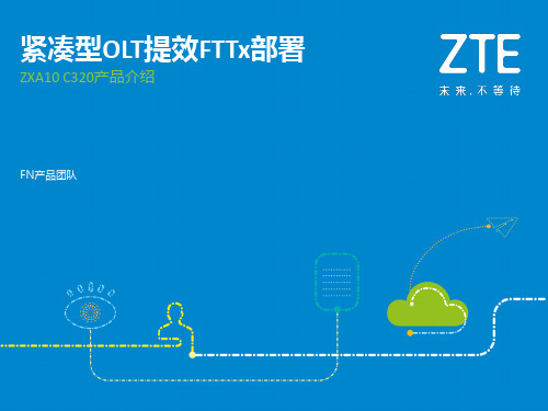
紧凑型OLT提效FTTx部署
ZXA10 C320产品介绍
FN产品团队
引领紧凑型OLT潮流
ZXA10 C320
• 2U高、19英寸宽、270mm深紧凑结构 • EPON/GPON/10G-EPON/XG-PON1/P2P统一 平台
• 用户侧典型配置8/16*PON板,最大提供32 PON
口
电信级高可靠性
以太网GE/10GE
OLT典型覆盖半径 5~10km
中心机房 ZXA10 C300 或汇聚交换机
方案优势
高集成度,容量适中
结构紧凑,便于运输和安装 低功耗、高可靠,降低供备 电、空调等配套要求;可室 外一体化部署,适应严苛环
OLT之间 10/40/80…km
OLT典型覆盖半径 5~10km
远端POP点A ZXA10 C320 远端POP点B ZXA10 C320 以太网10GE 各OLT之间 10/40/80…km 中心机房 ZXA10 C300
中兴ZXA10 xPON产品详细介绍PPT课件( 49页)

尺寸:88.1mm×482.6mm×240mm(高×宽×深) 供电:DC -48V,AC 220V 典型功耗:<75W
工作温度: -30~60℃
安装方式:机架、信息箱、配套室外机柜 业务槽位:支持4个业务槽位混插
(PR30/PRX30) - 光线路CES接口板(2口STM-1或1口STM4) - 32路E1平衡电路仿真板 - 32路T1平衡电路仿真板
面向下一代的中容量光接入平台
ZXA10 C220
面向下一代的EPON/GPON/10G EPON同平台架构设计,平滑演进 提供业界最丰富的GE光电/FE光电/10GE光/E1/STM-1等上联单板和EPON/GPON/10G
NetNumen N31
室外机柜
ODN
室内/外无源分光器 室内/外ONU综合配线产品 ODN器件
GPON MxU EPON MxU
F820 F821 F822 F803G 9806H 9816
F820 F821 F822 F402 F803 F809(电力) F829 9806H 9816
业界典范、共平台的全能产品ZXDSL 9806H
模块化交流/直流电源 交流供电+直流备电
调速风扇
选配EPON/GPON/10G EPON/GE/ 双PON/PON+GE上行
环境监控插座
2GE/FE+14FE用户板 24/48/64路POTS用户板 16/24路VDSL2用户板
24/32路ADSL2+用户板 8路ISDN用户板 4路E1用户板
ETSI:21英寸 IEC:19英寸
23个(21英寸) 21(19英寸)
21英寸:2块主控交换板+16块9U线卡 +2块4.5U上联卡+2块电源卡+1块时钟/
信任 40通道模拟输入场地终端集装箱(FTA)非爆炸性产品概述说明书

PD-T8831 TrustedTrusted 40 Channel Analogue FTA Non-Incendive Product OverviewThe Trusted® 40 Channel Analogue Input Field Termination Assembly (FTA) Non-Incendive T8831 is designed to act as the main interface between a non-incendive field device in a hazardous area generating an analogue signal and the Trusted TMR Analogue Input Module T8431. Features:•40 input channels per FTA.•Industry standard field device connections (2-wire).•Limited power for connection to non-incendive field wiring.•Standard DIN rail compatibility.•Simple installation and connection.•24 Vdc operation.•Fused field power supply per channel.•On-board Light Emitting Diode (LED) indication field power supply integrity.Trusted PD-T8831Page intentionally left blankPREFACEIn no event will Rockwell Automation be responsible or liable for indirect or consequential damages resulting from the use or application of this equipment. The examples given in this manual are included solely for illustrative purposes. Because of the many variables and requirements related to any particular installation, Rockwell Automation does not assume responsibility or reliability for actual use based on the examples and diagrams.No patent liability is assumed by Rockwell Automation, with respect to use of information, circuits, equipment, or software described in this manual.All trademarks are acknowledged.DISCLAIMERIt is not intended that the information in this publication covers every possible detail about the construction, operation, or maintenance of a control system installation. You should also refer to your own local (or supplied) system safety manual, installation and operator/maintenance manuals.REVISION AND UPDATING POLICYThis document is based on information available at the time of its publication. The document contents are subject to change from time to time. The latest versions of the manuals are available at the Rockwell Automation Literature Library under "Product Information" information "Critical Process Control & Safety Systems".TRUSTED RELEASEThis technical manual applies to Trusted Release: 3.6.1.LATEST PRODUCT INFORMATIONFor the latest information about this product review the Product Notifications and Technical Notes issued by technical support. Product Notifications and product support are available at the Rockwell Automation Support Centre atAt the Search Knowledgebase tab select the option "By Product" then scroll down and select the Trusted product.Some of the Answer ID’s in the Knowledge Base require a TechConnect Support Contract. For more information about TechConnect Support Contract Access Level and Features please click on the following link:https:///app/answers/detail/a_id/50871This will get you to the login page where you must enter your login details.IMPORTANT A login is required to access the link. If you do not have an account then you can create one using the "Sign Up" link at the top right of the web page.DOCUMENTATION FEEDBACKYour comments help us to write better user documentation. If you discover an error, or have a suggestion on how to make this publication better, send your comment to our technical support group at SCOPEThis manual specifies the maintenance requirements and describes the procedures to assist troubleshooting and maintenance of a Trusted system. WHO SHOULD USE THIS MANUALThis manual is for plant maintenance personnel who are experienced in the operation and maintenance of electronic equipment and are trained to work with safety systems. SYMBOLSIn this manual we will use these notices to tell you about safety considerations.SHOCK HAZARD: Identifies an electrical shock hazard. If a warning label is fitted, it can be on or inside the equipment.WARNING: Identifies information about practices or circumstances that can cause an explosion in a hazardous environment, which can cause injury or death, property damage or economic loss.ATTENTION: Identifies information about practices or circumstances that can cause injury or death.CAUTION: Identifies information about practices or circumstances that can cause property damage or economic loss.BURN HAZARD: Identifies where a surface can reach dangerous temperatures. If a warning label is fitted, it can be on or inside the equipment.This symbol identifies items which must be thought about and put in place when designing and assembling a Trusted controller for use in a Safety Instrumented Function (SIF). It appears extensively in the Trusted Safety Manual.IMPORTANTIdentifies information that is critical for successful application and understanding of the product.NOTE Provides key information about the product or service.TIP Tips give helpful information about using or setting up the equipment.WARNINGS AND CAUTIONSWARNING: EXPLOSION RISKDo not connect or disconnect equipment while the circuit is live or unless the area is known to be free of ignitable concentrations or equivalentAVERTISSEMENT - RISQUE D’EXPLOSIONNe pas connecter ou déconnecter l’équipement alors qu’il est sous tension, sauf si l’environnement est exempt de concentrations inflammables ou équivalenteMAINTENANCEMaintenance must be carried out only by qualified personnel. Failure to follow these instructions may result in personal injury.CAUTION: RADIO FREQUENCY INTERFERENCEMost electronic equipment is influenced by Radio Frequency Interference. Caution should be exercised with regard to the use of portable communications equipment around such equipment. Signs should be posted in the vicinity of the equipment cautioning against the use of portable communications equipment.CAUTION:The module PCBs contains static sensitive components. Static handling precautions must be observed. DO NOT touch exposed connector pins or attempt to dismantle a module.ISSUE RECORDIssue Date Comments6 Sep 05 Format7 Jun 16 Rebranded and updated to incorporate IEEE standards with correction oftypographical errors and also standardise the Relative Humidity Rangeand Operating Temperature statements in the Specification Section.Page intentionally left blankTrusted 40 Channel Analogue FTA Non-Incendive Table of Contents Table of Contents1.Description (3)2.Installation (5)3.Associated Cable Selection (7)4.Assembly Pinout Connections (9)4.1. PWR TB1 Connections (9)4.2. TB3 (Auxiliary Input) (9)4.3. TB2 (Field Terminals) (9)4.4. SK1 (11)5.Specifications (14)Table of Contents Trusted 40 Channel Analogue FTA Non-IncendivePage intentionally left blank1.DescriptionFigure 1 T8831 LayoutThe Trusted 40 Channel Analogue Input FTA Non-Incendive T8831 provides termination for a maximum of 40 input channels from various types of field devices which generate an analogue input. Figure 2 below shows the configuration of a single channel.Figure 2 Single Channel SchematicThe supply for the field is derived from dual 24 Vdc feeds which are ‘commoned’ via diodes on the FTA. Indication of the presence of the power supply is provided by a green LED. The supply is then fed to each channel.The supply voltage to the field is fed via the 145 Ω resistor. This effectively limits the current in the field loop allowing inputs from non-incendive field devices located in hazardous areas. The voltage developed across the 250 Ω resistor due to the incoming analogue signal from the field device is fed directly to the analogue input module.The cable linking the 40 channels on the input module to the FTA is terminated at the 96-way socket SK1. The dual dc field power supplies are connected to the FTA via a 5-way terminal block PWR TB. The input signals from the field (40-off) are connected by 2-wire arrangements terminated on 12-off 3-way terminal blocks and 2-off 2-way.2.InstallationTrusted 40 Channel Analogue Input FTA Non-Incendive T8831 is designed to be mounted on either of the TS32 or TS35 DIN rails in the horizontal or vertical positions as required.Page intentionally left blank3.Associated Cable SelectionRefer to the product descriptions detailed below: PD-TC000 Trusted Power CablesPD-TC200 Trusted I/O Companion Slot Cables PD-TC500 Trusted I/O SmartSlot CablesPage intentionally left blank4.Assembly Pinout Connections4.1.PWR TB1 ConnectionsPin Service1 24 V-A2 24 V-B3 0 V4 0 V5 24 V(auxiliary supply for use when required)Table 1 PWR TB1 Connections4.2.TB3 (Auxiliary Input)Pin Service1 Chan 0 (not configured)2 Chan 41(not configured)Table 2 TB3 (Auxiliary Input) Connections4.3.TB2 (Field Terminals)Pin Service Pin Service1 Chan 1 24 Vdc field supply2 Chan 1 signal from field3 Chan 2 24 Vdc field supply 4 Chan 2 signal from field5 Chan 3 24 Vdc field supply6 Chan 3 signal from field7 Chan 4 24 Vdc field supply 8 Chan 4 signal from field9 Chan 5 24 Vdc field supply 10 Chan 5 signal from field11 Chan 6 24 Vdc field supply 12 Chan 6 signal from field 13 Chan 7 24 Vdc field supply 14 Chan 7 signal from field 15 Chan 8 24 Vdc field supply 16 Chan 8 signal from field 17 Chan 9 24 Vdc field supply 18 Chan 9 signal from field 19 Chan 10 24 Vdc field supply 20 Chan 10 signal from field 21 Chan 11 24 Vdc field supply 22 Chan 11 signal from field 23 Chan 12 24 Vdc field supply 24 Chan 12 signal from field 25 Chan 13 24 Vdc field supply 26 Chan 13 signal from field 27 Chan 14 24 Vdc field supply 28 Chan 14 signal from field 29 Chan 15 24 Vdc field supply 30 Chan 15 signal from field 31 Chan 16 24 Vdc field supply 32 Chan 16 signal from field 33 Chan 17 24 Vdc field supply 34 Chan 17 signal from field 35 Chan 18 24 Vdc field supply 36 Chan 18 signal from field 37 Chan 19 24 Vdc field supply 38 Chan 19 signal from field 39 Chan 20 24 Vdc field supply 40 Chan 20 signal from field 41 Chan 21 24 Vdc field supply 42 Chan 21 signal from field 43 Chan 22 24 Vdc field supply 44 Chan 22 signal from field 45 Chan 23 24 Vdc field supply 46 Chan 23 signal from field 47 Chan 24 24 Vdc field supply 48 Chan 24 signal from field 49 Chan 25 24 Vdc field supply 50 Chan 25 signal from field 51 Chan 26 24 Vdc field supply 52 Chan 26 signal from field 53 Chan 27 24 Vdc field supply 54 Chan 27 signal from field 55 Chan 28 24 Vdc field supply 56 Chan 28 signal from field 57 Chan 29 24 Vdc field supply 58 Chan 29 signal from field59 Chan 30 24 Vdc field supply 60 Chan 30 signal from field61 Chan 31 24 Vdc field supply 62 Chan 31 signal from field63 Chan 32 24 Vdc field supply 64 Chan 32 signal from field65 Chan 33 24 Vdc field supply 66 Chan 33 signal from field67 Chan 34 24 Vdc field supply 68 Chan 34 signal from field69 Chan 35 24 Vdc field supply 70 Chan 35 signal from field71 Chan 36 24 Vdc field supply 72 Chan 36 signal from field73 Chan 37 24 Vdc field supply 74 Chan 37 signal from field75 Chan 38 24 Vdc field supply 76 Chan 38 signal from field77 Chan 39 24 Vdc field supply 78 Chan 39 signal from field79 Chan 40 24 Vdc field supply 80 Chan 40 signal from fieldTable 3 TB2 (Field Terminals) Connections4.4.SK1C B A1 SmartSlot Link C SmartSlot Link B SmartSlot Link A23 Chan 28 (+) Chan 14 (+) Chan 0 (+)4 Chan 28 (+) Chan 14 (+) Chan 0 (+)5 Chan 29 (+) Chan 15 (+) Chan 1 (+)6 Chan 29 (+) Chan 15 (+) Chan 1 (+)7 Chan 30 (+) Chan 16 (+) Chan 2 (+)8 Chan 30(+) Chan 16 (+) Chan 2 (+)9 0 V 0 V 0 V10 Chan 31 (+) Chan 17 (+) Chan 3 (+)C B A11 Chan 31 (+) Chan 17 (+) Chan 3 (+)12 Chan 32 (+) Chan 18 (+) Chan 4 (+)13 Chan 32 (+) Chan 18 (+) Chan 4 (+)14 Chan 33 (+) Chan 19 (+) Chan 5 (+)15 Chan 33 (+) Chan 19 (+) Chan 5 (+)16 Chan 34 (+) Chan 20 (+) Chan 6 (+)17 Chan 34 (+) Chan 20 (+) Chan 6 (+)18 Chan 35 (+) Chan 21 (+) Chan 7 (+)19 Chan35 (+) Chan 21 (+) Chan 7 (+)20 0 V 0 V 0 V21 Chan 36 (+) Chan 22 (+) Chan 8 (+)22 Chan 36 (+) Chan 22 (+) Chan 8 (+)23 Chan 37 (+) Chan 23 (+) Chan 9 (+)24 Chan 37 (+) Chan 23 (+) Chan 9 (+)25 Chan 38 (+) Chan 24 (+) Chan 10 (+)26 Chan 38 (+) Chan 24 (+) Chan 10 (+)27 Chan 39 (+) Chan 25 (+) Chan 11 (+)28 Chan 39 (+) Chan 25 (+) Chan 11 (+)29 Chan 40 (+) Chan 26 (+) Chan 12 (+)30 Chan 40 (+) Chan 26 (+) Chan 12 (+)31 Chan 41 (+) Chan 27 (+) Chan 13 (+)32 Chan 41 (+) Chan 27 (+) Chan 13 (+)Table 4 SK1 ConnectionsPage intentionally left blank5.SpecificationsVoltage Range 18 Vdc to 32 Vdc81 mAMaximum Normal Output Current I sc(Field Supply)32 V as voltage range aboveMaximum Normal Output Voltage V oc(Field Supply)Maximum External Capacitance C a 5 μF for methane0.3 μF for groups A and Bin accordance with AANSI/ISA 12.12.01-2000Maximum External Inductance L a10 mH for methane or group Bin accordance with AANSI/ISA 12.12.01-2000 Operating Temperature 0 °C to +60 °C (+32 °F to +140 °F)Non-operating Temperature -25 °C to +70 °C (-13 °F to +158 °F)10 % – 95 %, non-condensingRelative Humidity range(operating, storage and transport)Environmental Specifications Refer to Document 552517 DimensionsHeight 111 mm (4.4 in)Width 335 mm (13.2 in)Depth 51 mm (2 in)Weight 900 g (2 lb)。
- 1、下载文档前请自行甄别文档内容的完整性,平台不提供额外的编辑、内容补充、找答案等附加服务。
- 2、"仅部分预览"的文档,不可在线预览部分如存在完整性等问题,可反馈申请退款(可完整预览的文档不适用该条件!)。
- 3、如文档侵犯您的权益,请联系客服反馈,我们会尽快为您处理(人工客服工作时间:9:00-18:30)。
ZXTN19100CFF100V, SOT23F , NPN high gain power transistorSummaryBV CEX > 200V BV CEO > 100V BV ECO > 5V I C(cont) = 4.5A V CE(sat) < 60mV @ 1A R CE(sat) = 38m ⍀P D = 1.5WComplementary part number ZXTP19100CFFDescriptionAdvanced process capability has been used to maximise the performance of this transistor. The SOT23F package is compatible with the industry standard SOT23 footprint but offers lower profile and higher dissipation for applications where power density is of utmost importanceFeatures•High forward blocking voltage •Low saturation voltage •High gain•Low profile high dissipation packageApplications•Relay and solenoid driving •DC fans•Industrial and automotive switchingOrdering informationDevice marking1E5DeviceReel size(inches)Tape width (mm)Quantity per reel ZXTN19100CFFTA783000Absolute maximum ratingsParameter Symbol Limit Unit Collector-base voltage V CBO200V Collector-emitter voltage (forward blocking)V CEX200V Collector-emitter voltage V CEO100V Emitter-collector voltage (reverse blocking)V ECO5V Emitter-base voltage V EBO7V Continuous collector current(c)I C 4.5A Base current I B1A Peak pulse current I CM6A Power dissipation at T amb = 25°C(a)0.84Linear derating factor P D 6.72W Power dissipation at T amb = 25°C(b) 1.34mW/°C Linear derating factor P D10.72W Power dissipation at T amb = 25°C(c) 1.5mW/°C Linear derating factor P D12.0W Power dissipation at T amb = 25°C(d)2mW/°C Linear derating factor P D16.0W Operating and storage temperature range T j, T stg- 55 to 150°CThermal resistanceParameter Symbol Limit Unit Junction to ambient(a)R⍜JA149.3°C/W Junction to ambient(b)R⍜JA93.4°C/W Junction to ambient(c)R⍜JA83.3°C/W Junction to ambient(d)R⍜JA60°C/W NOTES:(a)For a device surface mounted on 15mm x 15mm x 1.6mm FR4 PCB with high coverage of single sided 1oz copper, instill air conditions.(b)Mounted on 25mm x 25mm x 1.6mm FR4 PCB with a high coverage of single sided 2 oz copper in still air conditions.(c)Mounted on 50mm x 50mm x 1.6mm FR4 PCB with a high coverage of single sided 2 oz copper in still air conditions.(d)As (c) above measured at t<5secs.CharacteristicsElectrical characteristics (at T amb = 25°C unless otherwise stated)ParameterSymbol Min.Typ.Max.Unit Conditions Collector-base breakdown voltageBV CBO 200240V I C = 100ACollector-emitter breakdown voltage (forward blocking)BV CEX 200240V I C = 100A, R BE < 1k ⍀ or -1V < V BE < 0.25V Collector-emitter breakdown voltage (base open)BV CEO 100120V I C = 10mA (*) NOTES:(*)Measured under pulsed conditions. Pulse width Յ300s; duty cycle Յ2%.Emitter-base breakdown voltageBV EBO 78.3V I E = 100AEmitter-collector breakdown voltage (reverse blocking)BV ECX 68.3V I E = 100A, R BC < 1k ⍀ or 0.25V > V BC > -0.25V Emitter-collector breakdown voltage (base open)BV ECO 58V I E = 100A, Collector-base cut-off currentI CBO<150nA V CB = 160V20A V CB = 160V, T amb = 100°C Collector-emitter cut-off current I CEX <1100nA V CE = 160V, R BE < 1k ⍀ or -1V < V BE < 0.25V Emitter-base cut-off current I EBO <150nA V EB = 5.6VCollector-emitter saturation voltageV CE(sat)4560mV I C = 1A, I B = 100mA (*)105135mV I C = 1A, I B = 20mA (*)170235mV I C = 4.5A, I B = 450mA (*)Base-emitter saturation voltage V BE(sat)9501050mV I C = 4.5A, I B = 450mA (*)Base-emitter turn-on voltageV BE(on)8801000mVI C = 4.5A, V CE = 2V (*)Static forward current transfer ratioh FE 200350500I C = 0.1A, V CE = 2V (*)130250I C = 1A, V CE = 2V (*)25I C = 5A, V CE = 2V (*)Transition frequency f T 150MHz I C = 100mA, V CE = 10Vf =50MHz Input capacitance C ibo 305pF V EB = 0.5V, f = 1MHz (*)Output capacitance C obo 15.725pF V CB = 10V, f = 1MHz (*)Delay time t d 28.3ns V CC = 10V. I C = 500mA, I B1 = I B2= 50mA.Rise time t r 23.6ns Storage time t s 962ns Fall timet f133nsIntentionally left blankPackage outline - SOT23FNote: Controlling dimensions are in millimeters. Approximate dimensions are provided in incheslimeters Inches limeters Inches Min.Max.Min.Max.Min.Max.Max.Max.A 0.80 1.000.03150.0394E 2.30 2.500.09060.0984A10.000.100.000.0043E1 1.50 1.700.05900.0669b 0.350.450.01530.0161E2 1.10 1.260.04330.0496c 0.100.200.00430.0079L 0.480.680.01890.0268D 2.80 3.000.11020.1181L10.300.500.01530.0161e 0.95 ref 0.0374 refR 0.050.150.00190.0059e11.802.000.07090.0787O0°12°0°12°Zetex sales offices EuropeZetex GmbHKustermann-park Balanstraße 59D-81541 München GermanyTelefon: (49) 89 45 49 49 0Fax: (49) 89 45 49 49 49europe.sales@AmericasZetex Inc700 Veterans Memorial Highway Hauppauge, NY 11788USATelephone: (1) 631 360 2222Fax: (1) 631 360 8222usa.sales@Asia PacificZetex (Asia Ltd)3701-04 Metroplaza Tower 1Hing Fong Road, Kwai Fong Hong KongTelephone: (852) 26100 611Fax: (852) 24250 494asia.sales@Corporate HeadquartersZetex Semiconductors plcZetex Technology Park, Chadderton Oldham, OL9 9LL United KingdomTelephone: (44) 161 622 4444Fax: (44) 161 622 4446hq@© 2007 Published by Zetex Semiconductors plcDefinitionsProduct changeZetex Semiconductors reserves the right to alter, without notice, specifications, design, price or conditions of supply of any product or service. Customers are solely responsible for obtaining the latest relevant information before placing orders.Applications disclaimerThe circuits in this design/application note are offered as design ideas. It is the responsibility of the user to ensure that the circuit is fit for the user’s application and meets with the user’s requirements. No representation or warranty is given and no liability whatsoever is assumed by Zetex with respect to the accuracy or use of such information, or infringement of patents or other intellectual property rights arising from such use or otherwise. Zetex does not assume any legal responsibility or will not be held legally liable (whether in contract,tort (including negligence), breach of statutory duty, restriction or otherwise) for any damages, loss of profit, business, contract,opportunity or consequential loss in the use of these circuit applications, under any circumstances.Life supportZetex products are specifically not authorized for use as critical components in life support devices or systems without the express written approval of the Chief Executive Officer of Zetex Semiconductors plc. As used herein:A. Life support devices or systems are devices or systems which:1.are intended to implant into the body or2.support or sustain life and whose failure to perform when properly used in accordance with instructions for use provided in the labeling can be reasonably expected to result in significant injury to the user.B. A critical component is any component in a life support device or system whose failure to perform can be reasonably expected tocause the failure of the life support device or to affect its safety or effectiveness.ReproductionThe product specifications contained in this publication are issued to provide outline information only which (unless agreed by the company in writing) may not be used, applied or reproduced for any purpose or form part of any order or contract or be regarded as a representation relating to the products or services concerned. Terms and ConditionsAll products are sold subjects to Zetex’ terms and conditions of sale, and this disclaimer (save in the event of a conflict between the two when the terms of the contract shall prevail) according to region, supplied at the time of order acknowledgement.For the latest information on technology, delivery terms and conditions and prices, please contact your nearest Zetex sales office.Quality of productZetex is an ISO 9001 and TS16949 certified semiconductor manufacturer.To ensure quality of service and products we strongly advise the purchase of parts directly from Zetex Semiconductors or one of our regionally authorized distributors. For a complete listing of authorized distributors please visit: /salesnetworkZetex Semiconductors does not warrant or accept any liability whatsoever in respect of any parts purchased through unauthorized sales channels.ESD (Electrostatic discharge)Semiconductor devices are susceptible to damage by ESD. Suitable precautions should be taken when handling and transporting devices.The possible damage to devices depends on the circumstances of the handling and transporting, and the nature of the device. The extent of damage can vary from immediate functional or parametric malfunction to degradation of function or performance in use over time.Devices suspected of being affected should be replaced.Green complianceZetex Semiconductors is committed to environmental excellence in all aspects of its operations which includes meeting or exceeding reg-ulatory requirements with respect to the use of hazardous substances. Numerous successful programs have been implemented to reduce the use of hazardous substances and/or emissions.All Zetex components are compliant with the RoHS directive, and through this it is supporting its customers in their compliance with WEEE and ELV directives.Product status key:“Preview”Future device intended for production at some point. Samples may be available “Active”Product status recommended for new designs “Last time buy (LTB)”Device will be discontinued and last time buy period and delivery is in effect “Not recommended for new designs”Device is still in production to support existing designs and production “Obsolete”Production has been discontinued Datasheet status key:“Draft version”This term denotes a very early datasheet version and contains highly provisional information, whichmay change in any manner without notice.“Provisional version”This term denotes a pre-release datasheet. It provides a clear indication of anticipated performance.However, changes to the test conditions and specifications may occur, at any time and without notice.“Issue”This term denotes an issued datasheet containing finalized specifications. However, changes tospecifications may occur, at any time and without notice.分销商库存信息: DIODESZXTN19100CFFTA。