MT2503_下载_开机_debug_SOP
WT2000 B03 模块使用说明书

广州唯创电子有限公司MP3录音模块WT2000B03模块V1.042020-09-10Note:WAYTRONIC ELECTRONIC CO.,LTD.reserves the right to change this document without prior rmation provided by WAYTRONIC is believed to be accurate and reliable.However,WAYTRONIC makes no warranty for any errors which may appear in this document.Contact WAYTRONIC to obtain the latest version of device specifications before placing your orders.No responsibility is assumed by WAYTRONIC for any infringement of patent or other rights of third parties which may result from its use.In addition,WAYTRONIC products are not authorized for use as critical components in life support devices/systems or aviation devices/systems,where a malfunction or failure of the product may reasonably be expected to result in significant injury to the user,WT2000B03模块使用说明书V1.04模块简介WT2000B03是一款功能强大的新型高品质MP3模块,从多方位满足客户的要求。
NS5S1153 DPDT USB 2.0高速 音频开关评估板用户手册说明书

NS5S1153MUGEVBDPDT USB 2.0 High Speed /Audio Switch with Negative Swing Capability Evaluation Board User's ManualOverviewThe NS5S1153 is a DPDT switch for combined true −ground audio and USB 2.0 high speed data applications. It allows portable systems to use a single port to pass either USB data or audio signals from an external headset; headset; the two channels being compliant to USB 2.0, USB 1.1 and USB 1.0.The switch is capable of passing signals with negative voltages as low as 2 V below ground. The device featuresshunt resistors on the audio ports. These resistors are switched in when the audio channel is off and provide a safe path to ground for any charge that may build up on the audio lines. This reduces Pop & Click noise in the audio system.The NS5S1153 is also equipped with V BUS detection circuitry to immediately switch to USB mode in the event that a voltage is detected on V BUS .The NS5S1153 is housed in a space saving, ultra low profile 1.4 x 1.8 x 0.5 mm 10 pin mQFN package.Figure 1. Board PictureEVAL BOARD USER’S MANUALNS5S1153 – BOARD SCHEMATICFigure 2. Board SchematicTable 1. NS5S1153 – BOARD CONNECTIONSSymbol Description SUPPLYV CC, GND This is the positive and the return connection for power supply. SETUPJ4 − ASEL This is the line selection header.J5 − VBUS_CTRL This is VBUS comparator input.SIGNALSJ1 − INPUT This USB connector Male A type is the common data and audio lines.J2 − AUDIO This connector is a 3.5 mm Stereo Jack Connector.J3 − USB This USB connector Male B type is the high speed USB signaling path.NS5S1153 – TEST PROCEDUREEquipment needed•Power Supply•Digital Ohm Meter•Desktop or Laptop with Windows XP or higher •USB Memory Stick •USB Type A to USB Type BTable 2. BACKGROUND: ASEL AND VBUS TRUTH TABLEA SEL V BUS L, R D+, D−L, R ShuntLow Low ON OFF OFFLow High OFF ON ONHigh X ON OFF OFF Test1.Connect ASEL to ‘0’ (J4) and VBUS_CTRL to ‘1’(J5).2.Connect the power supply at3.6 V from VCC to GND. The supply current should be around 20 m A. The impedance measured from COM+ (TP3) toD+ (TP5) is over 10 M W.The impedance measured from COM− (TP4) toD− (TP6) is over 10 M W.The impedance measured from COM+ (TP3) toR(TP7) is close to 3 W.The impedance measured from COM− (TP4) to L (TP8) is close to 3 W.3.Insert a USB cable from USB terminal (J3) to the laptop or desktop.The impedance measured from L (TP8) and R (TP7) to GND is closed to 118 W.4.Place a USB Memory Stick connected to USB terminal (J1). The device is being recognized.NS5S1153 – COMPONENTS SELECTIONInput CapacitorA 0.1 m F X5R ceramic capacitor or larger must bypass V CC input to the ground. This capacitor should be placed as close as possible to this input.ESD DiodeIn order to protect the device against transient voltages, an external bi−directional ESD / IEC diode is recommended on COM+ and COM− pin. The ESD11N is designed to protect voltage sensitive components that require ultra−low capacitance from ESD and transient voltage events. Excellent clamping capability, low capacitance, low leakage, and fast response time, make these parts ideal for ESD protection on designs where board space is at a premium. Because of its low capacitance, it is suited for use in high frequency designs such as USB 2.0 high speed and antenna line applications.Table 3. NS5S1153 – BILL OF MATERIALDesignator Qty Description Value Tolerance Footprint Manufacturer Manufacturer Part NumberU11NS5S1153n/a n/a UQFN10ON Semiconductor NS5S1153C11Ceramic CapacitorSMD1 m F10%0805Murata GRM155R60J105C21Ceramic CapacitorSMD0.01 m F10%0402D1, D2, D3, D4,D5, D665V Bi−DirectionalTVSn/a n/a DSN2ON Semiconductor ESD11N5TP3, TP4,TP5, TP6, TP7, TP8,TP97Test Point PC MultiPurposen/a n/a TP1Keystone Electronics5010VCC, GND2Banana Connector n/a n/a7 mm Hole JohnsonComponents111−2223−001Vbus_Ctrl, Asel250pin Modular 2pinheadern/a n/a Header3Tyco Electronics5−826629−0Input J11USB TypeAConnector n/a n/a USBTypeAMill−Max896−43−004−00−000000USB J31USB TypeBConnector n/a n/a USBTypeBAdam Tech USB−B−S−RAAudio J21Stereo Audio JackConnector n/a n/a PHONO_SJ3523CUI Inc SJ−3523−SMTGND Bar1PCB Shorting Link n/a n/a GND_StrapHarwin D3082−46PCB155 x 40 mm2 LayersNA NA NA Any NS5S1153MUGEVBNS5S1153 – PCB LAYOUT GUIDELINESElectrical Layout ConsiderationsImplementing a high speed USD device requires paying attention on USB lines and traces to preserve signal integrity. The demonstration board serves as layout example and can support the design engineers to preserve high speed performances.Electrical layout guidelines are:•Bypass capacitor must as closed as possible to the Vcc input pin for noise immunity•The characteristics impedance of each High Speed USB segment must be 45 W.•All corresponding D+ / D− line segment pairs must be the same length.•The use of vias to route these signals should be avoided.•The use of turns or bends to route these signal should be avoided.•The ground plane of the PCB will be used to determine the characteristics impedance of each line.NS5S1153 – EVALUATION BOARD PCB LAYOUT Board Reference: NS5S1153MUGEVBFigure 3. Assembly LayerFigure 4. Top Layer RoutingFigure 5. Bottom Layer RoutingADDITIONAL INFORMATIONTECHNICAL PUBLICATIONS :Technical Library: /design/resources/technical−documentation onsemi Website: ONLINE SUPPORT : /supportFor additional information, please contact your local Sales Representative at /support/sales。
智慧工地纯定位智能安全帽手册

便携式智能安全帽一、智能模块•产品简介智能模块是一款性价比高双星快速定位设备,主控平台MT2503提供GNSS秒定,业界第一Aiding GPS solution,内置GPS,北斗,快速到精准秒定位,支持2G通讯(中国移动/中国联通),支持GPRS数据通讯,sos求救功能,采集定位数据用GPRS数据发送到服务端,作为建筑工人打卡记录。
•产品规格(一)产品展示图:二、功能简介小巧的芯片,方便置入安全帽、腰带等随身穿戴物中。
高效智能的实现:人员定位、人员脱帽/倒地监测、SOS一键求救、全体语音通报、数据终端管理等施工项目中十分重要的功能。
不同职责的用户拥有不同权限的管理功能。
可直接查看项目系统内的工程项目信息,包括:项目基本信息、项目管理人员考勤信息、已完成务工人员实名登记的工人信息、实时在场工人总人数、不同工种和不同班组的登记人数和考勤信息等,保证信息的实时准确、真实透明。
2.1 产品功能智能安全帽对佩戴者进行实时数据收集系统,再对其进行智能统计筛选分析,管理人员通过手机和电脑即可对一线作业人员进行的远程控制。
2.2.1 劳务实名制管理进入现场施工的所有劳务人员建立个人档案,劳务人员个人档案存档至系统,并会及时更新。
采用人员穿戴设备智能安全帽,对人员进行实时管理。
系统先对人员进行录入操作,录入内容包括:施工人员的姓名、身份证号、性别、联系电话、民族、工种、单位、设备号、入职时间、班组、相关紧急联系人等信息。
2.2.2 定位功能实时定位,智能管控,可对人员的工作状态实时掌控。
轨迹查看,随时了解各人员最近时间段内的工作轨迹。
2.2.3 脱帽、倒地监测当现场人员未佩戴安全帽或者佩戴安全帽出现异常的时候,系统会发出警示,在项目地图上会有相对应的图标颜色进行显示;管理人员可根据实际情况进行现场检查并处理。
2.2.4 全体语音通告当需要语音通报的时候,管理人员勾选通知人员和通知的语音内容,点击发送,相关人员的智能安全帽实时接收语音提示内容。
SP4523锂电池充放电SOC V1.3说明书

概述SP4523是一款集成开关充电和同步升压功能的单芯片解决方案,内部集成了同步开关充电模块、同步升压放电管理模块、电量检测与LED 指示模块、保护模块。
SP4523内置充电与放电功率MOS ,充电电流为1A ,同步升压输出电流为1A 。
SP4523采用专利的充电电流自适应技术,同时采用专利的控制方式省去外部的功率设定电阻,降低功耗的同时降低系统成本。
SP4523内部集成了温度补偿、过温保护、过充与过放保护、输出过压保护、输出重载保护等多重安全保护功能以保证芯片和锂离子电池的安全,应用电路简单,只需很少元件便可实现充电管理与放电管理。
特点∙ 输出电流1A ∙ 充电电流:1A∙ 充电效率高达 94% ∙ 放电效率高达 94%∙ 无需昂贵的功率设定电阻 ∙ 充电电流自适应技术 ∙ 自动开关机∙ BAT 放电终止电压:2.9V ∙ 可选4.2V/4.35V充电电压 ∙ 智能温度控制与过温保护∙ 支持涓流模式以及零电压充电 ∙封装形式:ESOP8应用∙ 移动电源典型应用电路管脚管脚描述极限参数(注1)推荐工作范围注1:最大极限值是指超出该工作范围芯片可能会损坏。
推荐工作范围是指在该范围内芯片工作正常,但不完全保证满足个别性能指标。
电气参数定义了器件在工作范围内并且在保证特定性能指标的测试条件下的直流和交流电气参数规范。
对于未给定的上下限参数,该规范不予保证其精度,但其典型值合理反映了器件性能。
电气参数应用说明负载检测与低功耗智能待机负载插入时SP4523可以自动检测到负载并开启升压电路工作。
当负载电流低于25mA,经过16S延时,升压电路关闭,IC进入低电流待机模式。
充放电指示LED1外接指示LED灯,充电时,LED1以1Hz频率闪烁,电池充饱后LED1常亮;LED2外接指示LED灯,放电过程LED2常亮,当电池电压低于3.05V时,LED2会以1HZ频率闪烁进行低电报警提示。
电池低压保护启动时,当BAT电压大于3.2V时,升压电路开始工作,工作过程中如果电池电压低于3.05V,则LED1会以2HZ 频率快闪提醒电量较低,当电池电压低于2.9V,则放电输出关闭,SP4523进入低电流待机模式。
TB-FMCH-DP3 硬件用户手册说明书

TB-FMCH-DP3 Hardware User’s ManualRev.1.03Table of Contents1.Related Documents and Board Accessories (8)2.Overview (8)3.Feature (8)4.TB-FMCH-DP3 Function (9)4.1.Block Diagram (9)4.2.External View of the Board (10)4.3.Board Specification (11)4.4.Power Supply (12)4.4.1.IO Voltage (12)4.5.Source(TX) Block (13)4.6.Sink(RX) Block (14)4.7.Clock circuit (16)4.7.1.Operation example of PLL (17)4.8.FMC connector for stacking (18)4.9.Pin Assignment of CN4 (18)4.10.FMC connector for expanded Board (CN3) (29)List of TablesTable 4-1 Signals of Source Circuit (13)Table 4-2 DP130 I2C Address (13)Table 4-3 Signals of Sink Circuit (14)Table 4-4 DP159 I2C Address (15)Table 4-5 signals of PLL circuit (16)Table 4-6 PLL Resister settings (Step3) (17)Table 4-7 CN4 Pin assign (To carrier board) (19)Table 4-8 CN3 Pin assign (For expanded Board) (30)List of figuresFigure 3-1 High-pin Count Pin assignment (8)Figure 4-1 TB-FMCH-DP3 Block Diagram (9)Figure 4-2 Top view (10)Figure 4-3 bottom view (10)Figure 4-4 TB-FMCH-DP3 Dimension Diagram (11)Figure 4-5 Block diagram of Power Circuit (12)Figure 4-6 Voltage level shifter (12)Figure 4-7 Block Diagram of Source circuit (13)Figure 4-8 Block Diagram of Sink circuit (14)Figure 4-9 Block Diagram of PLL Circuit (16)Figure 4-10 Signal connection of stacking two boards. (18)Figure 4-11 Stacked boards (18)IntroductionThank you for purchasing the TB-FMCH-DP3 board. Before using the product, be sure to carefully read this user manual and fully understand how to correctly use the product. First read through this manual, then always keep it handy.SAFETY PRECAUTIONS Observe the precautions listed below to prevent injuries to you or other personnel or damage to property.∙ Before using the product, read these safety precautions carefully to assure correct use. ∙ These precautions contain serious safety instructions that must be observed. ∙ After reading through this manual, be sure to always keep it handy.The following conventions are used to indicate the possibility of injury/damage and classify precautions ifThe following graphical symbols are used to indicate and classify precautions in this manual. (Examples)DangerWarningCautionIn the event of a failure, disconnect the power supply.Do not use or place the product in the following locations.■DisclaimerThis product is an evaluation board for Displayport interface. Tokyo Electron Device Limited assumes no responsibility for any damages resulting from the use of this product for purposes other than those stated.Even if the product is used properly, Tokyo Electron Device Limited assumes no responsibility for any damages caused by:(1) Earthquake, thunder, natural disaster or fire resulting from the use beyond our responsibility, acts bya third party or other accidents, the customer’s willful or accidental misuse or use under otherabnormal conditions.(2) Secondary impact arising from use of this product or its unusable state (business interruption orothers)(3) Use of this product against the instructions given in this manual.(4) Malfunctions due to connection to other devices.Tokyo Electron Device Limited assumes no responsibility or liability for:(1) Erasure or corruption of data arising from use of this product.(2) Any consequences or other abnormalities arising from use of this product, or(3) Damage of this product not due to our responsibility or failure due to modificationThis product has been developed by assuming its use for research, testing or evaluation. It is not authorized for use in any system or application that requires high reliability.Repair of this product is carried out by replacing it on a chargeable basis, not repairing the faulty devices. However, non-chargeable replacement is offered for initial failure if such notification is received within two weeks after delivery of the product.The specification of this product is subject to change without prior notice.The product is subject to discontinuation without prior notice.1. Related Documents and Board AccessoriesRelated documents:All documents relating to this Board can be downloaded from our website. Please refer to attached paper of the products.Board Accessories:- Spacer set : x12. OverviewThe TB-FMCH-DP3 provides test environment for DisplayPort Standard Version1, Revision 2a.It supports below features4 Lane of 1.62Gbps, 2.7Gbps and 5.4GbpsIt uses TI SN75SP130 for Source(TX) and SN65DP159 for Sink(RX)AUX Communication.(FAUX is not supported)Also, it could stack up two TB-FMCH-DP3 for expand more channels.Notice: This board is used with Xilinx’s Displayport IP core.Some points are not tested because IP does not use.Question for IP core and reference design, please contact to Xilinx.3. FeatureDisplayPort Driver IC: Texas Instruments, SN75DP130SSDisplayPort Redriver IC: Texas Instruments, SN65DP159RGZPLLIC: Texas Instruments, LMK04906DisplayPort connector: JAE, DP1RD20JQ1R400 or Molex, 47272-0024FMC connector: Samtec, ASP-134488-01 / ASP-134486-01Figure 3-1 High-pin Count Pin assignment4. TB-FMCH-DP3 Function4.1. Block DiagramThe following figure shows the block diagram of this Board.CN4 is mounted to bottom side and it will connect to FPGA Evaluation boards.Please see more detail of each circuit.PLLDisplayPort RXDisplayPort TXFigure 4-1 TB-FMCH-DP3 Block Diagram4.2. External View of the BoardThe following figures show the external views of the Board.RXTXPLLDisplayPort Equalizer/DriverFMC-HPC for stacked board FMC (CN3)DisplayPortConnectorFigure 4-2 Top viewFMC-HPCfor Platform 基板FMC (CN4)Figure 4-3 bottom view4.3. Board SpecificationExternal Dimensions: W:78.8mm x H:69.0mmNumber of Layers: 8 LayersBoard Thickness: 1.6mmMaterial: MEG-6(R-5775) or same specification.Figure 4-4 TB-FMCH-DP3 Dimension Diagram4.4. Power SupplyThis board generates required voltage(1.1V) of DP139 from +3.3V is coming from FMC Connector. Following is block diagram of power circuit.1.1VI/O InputInputFigure 4-5 Block diagram of Power Circuit4.4.1. IO VoltageThis board has a voltage level shifter for required signals.FPGA IO voltage should be connected via FMC_VADJ on Carrier board.Figure 4-6 Voltage level shifterFollowing figure shows block diagram of Source circuit. DP130 keep signal integrity before transfer signal via cable and it can change swing level and pre-emphasis by AUX communication.Figure 4-7 Block Diagram of Source circuit.Table 4-1 Signals of Source CircuitAccessing to DP130 via I2C interface.It is possible to accessing DP130 via I2C interface. About I2C address please refer to below table. Note: Basically, it is controlled by AUX communication. I2C access is not required.Table 4-2 DP130 I2C AddressFollowing figure shows block diagram of Sink circuit. DP159 keep signal integrity as swing level and jitter.Figure 4-8 Block Diagram of Sink circuitTable 4-3 Signals of Sink Circuit(*) SINK_AUX_RX/TX signals are added from board Rev2.2.Accessing to DP159 via I2C interface.It is possible to accessing DP159 via I2C interface. About I2C address please refer to below table. Note: It is required to access DP159 via I2C. setting is depended on AUX communication.Xilinx Displayport IP supports DP159 and I2C control.Table 4-4 DP159 I2C Address4.7. Clock circuitFollowing block diagram shows PLL circuit.PLL device is TI “LMK04906” to generating reference clock of FPGAFigure 4-9 Block Diagram of PLL CircuitTable 4-5 signals of PLL circuit4.7.1. Operation example of PLLThis section described how to set resister of PLL for generating 135MHz, 81MHz, 162MHz and 270MHz.1) Enable resister change: Write 0x0000001F to R312) Reset to PLL: write 0x00200000 to R003) Set following settings to each resister.Table 4-6 PLL Resister settings (Step3)4) Disable resister change: write 0x0000003F to R31For more detail, please refer to data sheet.4.8. FMC connector for stackingThis board has two FMC connectors. One is connecting to FPGA Evaluation board and other is stacking same TB-FMCH-DP3 board.In this section, it shows that lower FMC is “base board ” and upper FMC is “stack board ”.Following figure shows signal connection when stacking two boards.Signal of stack board will connect CN3 of base board then signal name is changed as “EX_***”. “EX_***” signals connect to FPGA carrier board via CN4 of base board.An exception, PLL control signal and clock are not connecting to FPGA carrier board via base board.SINK_LANE(x4)EX_SINK_LANE(x4)SOURCE_LANE(x4)EX_SOURCE_LANE(x4)DisplayPort I/O MicrowireStarus CLKOUT0Clean clock(27MHz)PLLBoardBoard etc ...Figure 4-10 Signal connection of stacking two boards.Base BoardStack BoardFigure 4-11 Stacked boardsCation: Please confirm the notice of TB-FMCH-DP3.4.9. Pin Assignment of CN4Table 4-7 CN4 Pin assign (To carrier board) shows FMC pin assignment. Signal direction is assigned as follows:-“I”: The signal came from carrier board to TB-FMCH-DP3. -“O”: The signal came from TB-FMCH-DP3 to carrier board.Blue Character signal are connected to CN4 FMC Expansion connector.Table 4-7 CN4 Pin assign (To carrier board)4.10. FMC connector for expanded Board (CN3)From next page, Table 4-8 CN3 Pin assign (For expanded Board) shows FMC pin assignment. Signal direction is assigned as follows:-“I”: The signal came from carrier board to TB-FMCH-DP3.-“O”: The signal came from TB-FMCH-DP3 to carrier board.Table 4-8 CN3 Pin assign (For expanded Board)Inrevium Company。
MTK我的维修经验总结对你绝对有用

CI-B03GT04S-MT模块数据手册说明书

Chipintelli Technology Co.,Ltd.CONFIDENTIAL ALL RIGHTS RESERVED.This document is not to be reproduced,modified,adapted,published,translated in any material form in whole or in part nor disclosed to any third party without the priorwritten permission of Chipintelli Technology Co.,Ltd.文档分类:硬件开发文档名称:CI-B03GT04S-MT 模块数据手册文档日期:2021/02/23请点击此处下载本文档的PDF版本CI-B03GT04S-MT模块数据手册模块介绍概述本模块是针对离在线语音应用方案开发的一款通用、便携、低功耗高性能的带WIFI的语音识别模块,型号为:CI-B03GT04S-MT,模块的主芯片为CI1103,支持本地300条命令词以下的离在线语音识别。
图1 模块原理框图本模块具有以下特点:模块支持离在线应用,体积较小,长宽为47mm×32mm,工作电压为4.5V-5.5V,板载一颗8MB NorFlash(语音识别芯片系统使用)和一颗4MB NorFlash(WIFI芯片系统使用),带2路麦克风接口、1路HP_Audio接口、2路5V电源输入接口(语音识别芯片系统、WIFI芯片系统各1路)、1路3.3V电源输出接口、1路IIS接口、1路I2C接口、2路UART接口及3路PWM接口。
模块需搭配带有音频功放、麦克风和扬声器等外围器件的底板或客户功能板使用,由底板或客户功能板提供5V电源,上位机等外部对接系统进行UART或GPIO通讯和控制。
模块自带2支板载PCB天线,支持WIFI和BLE应用。
模块支持3.3V电源输出,输出电流不超过50mA。
PMK 8 PMK 6 PMK 3 快速启动向导说明书
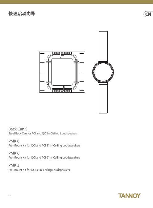
Back Can SSteel Back Can for PCI and QCI In-Ceiling Loudspeakers PMK 8Pre-Mount Kit for QCI and PCI 8" In-Ceiling Loudspeakers PMK 6Pre-Mount Kit for QCI and PCI 6" In-Ceiling Loudspeakers PMK 3Pre-Mount Kit for QCI 3" In-Ceiling LoudspeakersV 1.0带有此标志的终端设备具有强大的电流, 存在触电危险。
仅限使用带有 ¼'' TS 或扭锁式插头的高品质专业扬声器线。
所有的安装或调整均须由合格的专业人员进行。
此标志提醒您, 产品内存在未绝缘的危险电压, 有触电危险。
此标志提醒您查阅所附的重要的使用及维修说明。
请阅读有关手册。
小心为避免触电危险, 请勿打开机顶盖 (或背面挡板)。
设备内没有可供用户维修使用的部件。
请将维修事项交由合格的专业人员进行。
小心为避免着火或触电危险, 请勿将此设备置于雨淋或潮湿中。
此设备也不可受液体滴溅, 盛有液体的容器也不可置于其上, 如花瓶等。
小心维修说明仅是给合格的专业维修人员使用的。
为避免触电危险, 除了使用说明书提到的以外, 请勿进行任何其它维修。
所有维修均须由合格的专业人员进行。
1. 请阅读这些说明。
2. 请妥善保存这些说明。
3. 请注意所有的警示。
4. 请遵守所有的说明。
5. 请勿在靠近水的地方使用本产品。
6. 请用干布清洁本产品。
7. 请勿堵塞通风口。
安装本产品时请遵照厂家的说明。
8. 请勿将本产品安装在热源附近,如 暖 气 片, 炉子或其它产生热量的设备( 包 括功放器)。
9. 请勿移除极性插头或接地插头的安全装置。
接地插头是由两个插塞接点及一个接地头构成。
- 1、下载文档前请自行甄别文档内容的完整性,平台不提供额外的编辑、内容补充、找答案等附加服务。
- 2、"仅部分预览"的文档,不可在线预览部分如存在完整性等问题,可反馈申请退款(可完整预览的文档不适用该条件!)。
- 3、如文档侵犯您的权益,请联系客服反馈,我们会尽快为您处理(人工客服工作时间:9:00-18:30)。
Download issue Debug Follow1/3
PC drive
MT6261HW SCH
MT6261 can power on in min system mode
MT6261 ok
3333 HW SCH
INTERNAL USE
loginid=huangchen@,time=2016-07-22 15:12:11,ip=113.99.87.20,doctitle=MT2503 下载_开机 debug SOP.pptx,company=VSUN_WCX
KROW2 (pin C10)
loginid=huangchen@,time=2016-07-22 15:12:11,ip=113.99.87.20,doctitle=MT2503 下载_开机 debug SOP.pptx,company=VSUN_WCX
Case2@GPS DL Fail
MT6261 KCOL4 (pin D11) KCOL3 (pin D9) KROW4 (pin E9) KROW3 (pin D8)
INTERNAL USE
MT3333 GNSS_UART_TX (pin M16) GNSS_TXIND (pin E18) GNSS_UART_RX (pin K16) GPS_32K (pin A17) GPS_LDO_EN (to external LDO of enable)
Issue Description
MT6261 dl ok but MT333 DL fail ,No Respond
Root cause
Test GPS AVDD43_VBAT power is 0V(should be 3.3V),Review Customer SCH Customer change GPS LDO enable pin to another GPIO ,So Flash tool can’t enable GPS power. GPS SCH design should as follow table :
Power on issue Debug Follow2/2
Please follow bellow table to check MT2503 Hardware design and output signal ,if all of them is ok ,but still can not power on ,please ask Mediatek support team for help immediately ,thanks
INTERNAL USE
loginid=huangchen@,time=2016-07-22 15:12:11,ip=113.99.87.20,doctitle=MT2503 下载_开机 debug SOP.pptx,company=VSUN_WCX
Power on issue Debug Follow1/2
Issue Description
MT6261 dl ok but MT333 DL fail in stress test ,GPS Download No Respond
Root cause
Flash tool use 32k CLK before MT6261 Finish 32k Calibration in sometimes ,so HW test 32k is 37K(or other frequency),in this time ,GPS download will be fail . Update flash After W1613 .
download pass fail HW issue ready ok SW log power on debug sop download ok power
Double check HW Signal
INTERNAL USE
loginid=huangchen@,time=2016-07-22 15:12:11,ip=113.99.87.20,doctitle=MT2503 下载_开机 debug SOP.pptx,company=VSUN_WCX
INTERNAL USE
loginid=huangchen@,time=2016-07-22 15:12:11,ip=113.99.87.20,doctitle=MT2503 下载_开机 debug SOP.pptx,company=VSUN_WCX
Download issue HW Check list—GPS(3/3)
INTERNAL USE
MT2503 Download Debug SOP V0.1
loginid=huangchen@,time=2016-07-22 15:12:11,ip=113.99.87.20,doctitle=MT2503 下载_开机 debug SOP.pptx,company=VSUN_WCX
Please follow bellow table to check GPS Hardware design and output signal ,if all of them is ok ,but still can not Download ,please ask Mediatek support team for help immediately ,thanks
Download issue HW Check list—BB(2/3)
Please follow bellow table to check BB Hardware design and output signal ,if all of them is ok ,but still can not Download ,please ask Mediatek support team for help immediately ,thanks
loginid=huangchen@,time=2016-07-22 15:12:11,ip=113.99.87.20,doctitle=MT2503 下载_开机 debug SOP.pptx,company=VSUN_WCX
INTERNAL USE
loginid=huangchen@,time=2016-07-22 15:12:11,ip=113.99.87.20,doctitle=MT2503 下载_开机 debug SOP.pptx,company=VSUN_WCX
INTERNAL USE
loginid=huangchen@,time=2016-07-22 15:12:11,ip=113.99.87.20,doctitle=MT2503 下载_开机 debug SOP.pptx,company=VSUN_WCX
Case3@GPS DL Fail
Issue Description
MT6261 dl ok but MT333 DL fail ,No Respond
Root cause
Test GPS TCXO power(GPS GNSS_TCXO_SW)is 0v(should be 2.8V) ,test GPS other powers is ok Review Customer SCH ,and find customer use crystal for TCXO ,so ,GPS TCXO power short to GND . Change Components from crystal to TCXO ,download is ok .
INTERNAL USE
loginid=huangchen@,time=2016-07-22 15:12:11,ip=113.99.87.20,doctitle=MT2503 下载_开机 debug SOP.pptx,company=VSUN_WCX
Case1@GPS DL Fail
Direction of MT6261 INPUT INPUT OUTOUT OUTOUT OUTOUT
Note Don’t change to other pin
Don’t change to other pin Don’t change to other pin Don’t change to other pin
INTERNAL USE
loginid=huangchen@,time=2016-07-22 15:12:11,ip=113.99.87.20,doctitle=MT2503 下载_开机 debug SOP.pptx,company=VSUN_WCX
Appendix
INTERNAL USE