MAX1441 美信(Maxim)最新电容检测芯片
备战2013电子设计大赛1

备战2013电子设计竞赛在电子设计竞赛作品中,ADC几乎是一个不可缺少的部分之一。
下面介绍ADC的选择时需要考虑的一些因素。
1. ADC的分类常用的ADC有积分型、逐次逼近型、并行比较型/串并行型、Σ-Δ调制型、电容阵列逐次比较型及压频变换型。
(1)积分型积分型ADC工作原理是将输入电压转换成时间(脉冲宽度信号)或频率(脉冲频率),然后由定时器/计数器获得数字值。
优点是具有高分辨率,缺点是由于转换精度依赖于积分时间,因此转换速率低。
例如TLC7135等。
(2)逐次比较型逐次比较型ADC由一个比较器和DAC通过逐次比较逻辑构成,从MSB开始,顺序地对每一位将输入电压与内置DAC输出进行比较,经n次比较而输出数字值。
优点是速度较高、功耗低,在低分辨率(<12位)时价格便宜,但高精度(>12位)时价格很高。
例如TLC0831等。
(3)并行比较型/串并行比较型(Flash(快速))并行比较型ADC采用多个比较器,仅作一次比较而实行转换。
由于转换速率极高,n位的转换需要2n-1个比较器,因此电路规模也极大,价格也高,适用于视频A/D转换器等速度特别高的领域。
串并行比较型ADC结构上介于并行型和逐次比较型之间,最典型的是由2个n/2位的并行型ADC配合DAC组成,用两次比较实行转换,所以称为Half flash(半快速)型。
还有分成三步或多步来实现A/D转换的叫做分级(Multistep/Subrangling)型ADC,而从转换时序角度又可称为流水线(Pipelined)型ADC,现代的分级型ADC中还加入了对多次转换结果作数字运算而修正特性等功能。
这类ADC速度比逐次比较型高,电路规模比并行型小。
例如TLC5510等。
(4)Σ-Δ调制型Σ-Δ型ADC由积分器、比较器、1位DAC和数字滤波器等组成。
原理上近似于积分型,将输入电压转换成时间(脉冲宽度)信号,用数字滤波器处理后得到数字值。
因此具有高分辨率,主要用于音频和测量。
比较器的合理选择
比较器的合理选择摘要:本文说明比较器的特性、指标以及比较器与运算放大器差异。
其中包括内置基准的比较器应用电路和利用双比较器构建窗检测器、利用四比较器解决电压或电流测量问题的电路。
长期以来,受运算放大器的影响,比较器的应用一直没有得到应有的重视。
直到目前随着比较器性能指标的改进,使其更好地胜任电压比较这一基本任务,这一状况才得到改善,本文主要介绍新型比较器的性能及其典型应用。
比较器的功能比较器的两路输入为模拟信号,输出则为二进制信号,当输入电压的差值增大或减小时,其输出保持恒定。
从这一角度来看,也可以将比较器当作一个1位模/数转换器(ADC)。
比较器与运算放大器运算放大器在不加负反馈时,从原理上讲可以用作比较器,但由于运算放大器的开环增益非常高,它只能处理输入差分电压非常小的信号。
而且,在这种情况下,运算放大器的响应时间比比较器慢许多,而且也缺少一些特殊功能,如:滞回、内部基准等。
比较器通常不能用作运算放大器,比较器经过调节可以提供极小的时间延迟,但其频响特性受到一定限制,运算放大器正是利用了频响修正这一优势而成为灵活多用的器件。
另外,许多比较器还带有内部滞回电路,这避免了输出振荡,但同时也使其不能当作运算放大器使用。
电源电压比较器与运算放大器工作在同样的电源电压,传统的比较器需要±15V等双电源供电或高达36V的单电源供电,这些产品在工业控制中仍有需求,许多厂商也仍在提供该类产品。
但是,从市场发展趋势看,目前大多数应用需要比较器工作在电池电压所允许的单电源电压范围内,而且,比较器必须具有低电流、小封装,有些应用中还要求比较器具有关断功能。
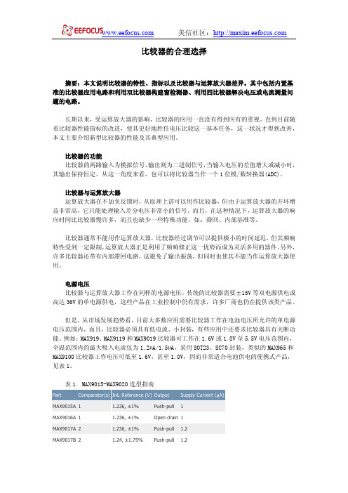
例如:MAX919、MAX9119和MAX9019比较器可工作在1.6V或1.8V至5.5V电压范围内,全温范围内的最大吸入电流仅为1.2µA/1.5µA,采用SOT23、SC70封装,类似的MAX965和MAX9100比较器工作电压可低至1.6V,甚至1.0V,因而非常适合电池供电的便携式产品,见表1。
MAXIM芯片大全

MAXIM/DALLAS 中文数据资料DS12CR887, DS12R885, DS12R887 RTC,带有恒压涓流充电器DS1870 LDMOS RF功放偏置控制器DS1921L-F5X Thermochron iButtonDS1923 温度/湿度记录仪iButton,具有8kB数据记录存储器DS1982, DS1982-F3, DS1982-F5 1k位只添加iButton?DS1990A 序列号iButtonDS1990R, DS1990R-F3, DS1990R-F5 序列号iButtonDS1991 多密钥iButtonDS2129 LVD SCSI 27线调节器DS2401 硅序列号DS2406 双通道、可编址开关与1k位存储器DS2408 1-Wire、8通道、可编址开关DS2411 硅序列号,带有VCC输入DS2413 1-Wire双通道、可编址开关DS2430A 256位1-Wire EEPROMDS2431 1024位、1-Wire EEPROMDS2480B 串行、1-Wire线驱动器,带有负荷检测DS2482-100 单通道1-Wire主控制器DS2482-100 勘误表PDF: 2482-100A2DS2482-800, DS2482S-800 八通道1-Wire主控制器DS2482-800 勘误表PDF: 2482-800A2DS2502 1k位只添加存储器DS2505 16k位只添加存储器DS28E04-100 4096位、可寻址、1-Wire EEPROM,带有PIO DS3170DK DS3/E3单芯片收发器开发板DS3231, DS3231S 高精度、I2C集成RTC/TCXO/晶振DS33Z44 四路以太网映射器DS3902 双路、非易失、可变电阻器,带有用户EEPROMDS3906 三路、非易失、小步长调节可变电阻与存储器DS3984 4路冷阴极荧光灯控制器DS4302 2线、5位DAC,提供三路数字输出DS80C400-KIT DS80C400评估套件DS80C410, DS80C411 具有以太网和CAN接口的网络微控制器DS80C410 勘误表PDF: 80C410A1DS89C430, DS89C440, DS89C450 超高速闪存微控制器DS89C430 勘误表PDF: 89C430A2DS89C440 勘误表PDF: 89C440A2DS89C450 勘误表PDF: 89C450A2DS89C430 勘误表PDF: 89C430A3DS89C440 勘误表PDF: 89C440A3DS89C450 勘误表PDF: 89C450A3DS89C430 勘误表PDF: 89C430A5DS89C440 勘误表PDF: 89C440A5DS89C450 勘误表PDF: 89C450A5DS9090K 1-Wire器件评估板, B版DS9097U-009, DS9097U-E25, DS9097U-S09 通用1-Wire COM端口适配器DS9490, DS9490B, DS9490R USB至1-Wire/iButton适配器MAX1034, MAX1035 8/4通道、±VREF多量程输入、串行14位ADCMAX1072, MAX1075 1.8Msps、单电源、低功耗、真差分、10位ADCMAX1076, MAX1078 1.8Msps、单电源供电、低功耗、真差分、10位ADC,内置电压基准MAX1146, MAX1147, MAX1148, MAX1149 多通道、真差分、串行、14位ADC MAX1149EVKIT MAX1149评估板/评估系统MAX1220, MAX1257, MAX1258 12位、多通道ADC/DAC,带有FIFO、温度传感器和GPIO端口MAX1224, MAX1225 1.5Msps、单电源、低功耗、真差分、12位ADCMAX1258EVKIT MAX1057, MAX1058, MAX1257, MAX1258评估板/评估系统MAX1274, MAX1275 1.8Msps、单电源、低功耗、真差分、12位ADCMAX13000E, MAX13001E, MAX13002E, MAX13003E, MAX13004E, MAX13005E 超低电压电平转换器MAX1302, MAX1303 8/4通道、±VREF多量程输入、串行16位ADCMAX1304, MAX1305, MAX1306, MAX1308, MAX1309, MAX1310, MAX1312, MAX1313, MAX1314 8/4/2通道、12位、同时采样ADC,提供±10V、±5V或0至+5V模拟输入范围MAX13050, MAX13052, MAX13053, MAX13054 工业标准高速CAN收发器,具有±80V故障保护MAX13080E, MAX13081E, MAX13082E, MAX13083E, MAX13084E, MAX13085E, MAX13086E, MAX13087E, MAX13088E, MAX13089E +5.0V、±15kV ESD保护、失效保护、热插拔、RS-485/RS-422收发器MAX13101E, MAX13102E, MAX13103E, MAX13108E 16通道、带有缓冲的CMOS 逻辑电平转换器MAX1334, MAX1335 4.5Msps/4Msps、5V/3V、双通道、真差分10位ADCMAX1336, MAX1337 6.5Msps/5.5Msps、5V/3V、双通道、真差分8位ADCMAX13481E, MAX13482E, MAX13483E ±15kV ESD保护USB收发器, 外部/内部上拉电阻MAX1350, MAX1351, MAX1352, MAX1353, MAX1354, MAX1355, MAX1356, MAX1357 双路、高端、电流检测放大器和驱动放大器MAX1450 低成本、1%精确度信号调理器,用于压阻式传感器MAX1452 低成本、精密的传感器信号调理器MAX1487, MAX481, MAX483, MAX485, MAX487, MAX488, MAX489, MAX490, MAX491 低功耗、限摆率、RS-485/RS-422收发器MAX1492, MAX1494 3位半和4位半、单片ADC,带有LCD驱动器MAX1494EVKIT MAX1493, MAX1494, MAX1495评估板/评估系统MAX1497, MAX1499 3位半和4位半、单片ADC,带有LED驱动器和μC接口MAX1499EVKIT MAX1499评估板/评估系统MAX15000, MAX15001 电流模式PWM控制器, 可调节开关频率MAX1515 低电压、内置开关、降压/DDR调节器MAX1518B TFT-LCD DC-DC转换器, 带有运算放大器MAX1533, MAX1537 高效率、5路输出、主电源控制器,用于笔记本电脑MAX1533EVKIT MAX1533评估板MAX1540A, MAX1541 双路降压型控制器,带有电感饱和保护、动态输出和线性稳压器MAX1540EVKIT MAX1540评估板MAX1551, MAX1555 SOT23、双输入、USB/AC适配器、单节Li+电池充电器MAX1553, MAX1554 高效率、40V、升压变换器,用于2至10个白光LED驱动MAX1556, MAX1557 16μA IQ、1.2A PWM降压型DC-DC转换器MAX1556EVKIT MAX1556EVKIT评估板MAX1558, MAX1558H 双路、3mm x 3mm、1.2A/可编程电流USB开关,带有自动复位功能MAX1586A, MAX1586B, MAX1586C, MAX1587A, MAX1587C 高效率、低IQ、带有动态内核的PMIC,用于PDA和智能电话MAX16801A/B, MAX16802A/B 离线式、DC-DC PWM控制器, 用于高亮度LED驱动器MAX1858A, MAX1875A, MAX1876A 双路180°异相工作的降压控制器,具有排序/预偏置启动和PORMAX1870A 升/降压Li+电池充电器MAX1870AEVKIT MAX1870A评估板MAX1874 双路输入、USB/AC适配器、1节Li+充电器,带OVP与温度调节MAX1954A 低成本、电流模式PWM降压控制器,带有折返式限流MAX1954AEVKIT MAX1954A评估板MAX19700 7.5Msps、超低功耗模拟前端MAX19700EVKIT MAX19700评估板/评估系统MAX19705 10位、7.5Msps、超低功耗模拟前端MAX19706 10位、22Msps、超低功耗模拟前端MAX19707 10位、45Msps、超低功耗模拟前端MAX19708 10位、11Msps、超低功耗模拟前端MAX2041 高线性度、1700MHz至3000MHz上变频/下变频混频器,带有LO缓冲器/开关MAX2043 1700MHz至3000MHz高线性度、低LO泄漏、基站Rx/Tx混频器MAX220, MAX222, MAX223, MAX225, MAX230, MAX231, MAX232, MAX232A, MAX233, MAX233A, MAX234, MAX235, MAX236, MAX237, MAX238, MAX239, MAX240, MAX241, MAX242, MAX243, MAX244, MAX245, MAX246, MAX247, MAX248, MAX249 +5V供电、多通道RS-232驱动器/接收器MAX2335 450MHz CDMA/OFDM LNA/混频器MAX2370 完备的、450MHz正交发送器MAX2370EVKIT MAX2370评估板MAX2980 电力线通信模拟前端收发器MAX2986 集成电力线数字收发器MAX3013 +1.2V至+3.6V、0.1μA、100Mbps、8路电平转换器MAX3205E, MAX3207E, MAX3208E 双路、四路、六路高速差分ESD保护ICMAX3301E, MAX3302E USB On-the-Go收发器与电荷泵MAX3344E, MAX3345E ±15kV ESD保护、USB收发器,UCSP封装,带有USB检测MAX3394E, MAX3395E, MAX3396E ±15kV ESD保护、大电流驱动、双/四/八通道电平转换器, 带有加速电路MAX3535E, MXL1535E +3V至+5V、提供2500VRMS隔离的RS-485/RS-422收发器,带有±15kV ESD保护MAX3570, MAX3571, MAX3573 HI-IF单芯片宽带调谐器MAX3643EVKIT MAX3643评估板MAX3645 +2.97V至+5.5V、125Mbps至200Mbps限幅放大器,带有信号丢失检测器MAX3654 47MHz至870MHz模拟CATV互阻放大器MAX3654EVKIT MAX3654评估板MAX3657 155Mbps低噪声互阻放大器MAX3658 622Mbps、低噪声、高增益互阻前置放大器MAX3735, MAX3735A 2.7Gbps、低功耗、SFP激光驱动器MAX3737 多速率激光驱动器,带有消光比控制MAX3737EVKIT MAX3737评估板MAX3738 155Mbps至2.7Gbps SFF/SFP激光驱动器,带有消光比控制MAX3744, MAX3745 2.7Gbps SFP互阻放大器,带有RSSIMAX3744EVKIT, MAX3745EVKIT MAX3744, MAX3745评估板MAX3748, MAX3748A, MAX3748B 紧凑的、155Mbps至4.25Gbps限幅放大器MAX3785 6.25Gbps、1.8V PC板均衡器MAX3787EVKIT MAX3787评估板MAX3793 1Gbps至4.25Gbps多速率互阻放大器,具有光电流监视器MAX3793EVKIT MAX3793评估板MAX3805 10.7Gbps自适应接收均衡器MAX3805EVKIT MAX3805评估板MAX3840 +3.3V、2.7Gbps双路2 x 2交叉点开关MAX3841 12.5Gbps CML 2 x 2交叉点开关MAX3967 270Mbps SFP LED驱动器MAX3969 200Mbps SFP限幅放大器MAX3969EVKIT MAX3969评估板MAX3982 SFP铜缆预加重驱动器MAX3983 四路铜缆信号调理器MAX3983EVKIT MAX3983评估板MAX3983SMAEVKIT MAX3983 SMA连接器评估板MAX4079 完备的音频/视频后端方案MAX4210, MAX4211 高端功率、电流监视器MAX4210EEVKIT MAX4210E、MAX4210A/B/C/D/F评估板MAX4211EEVKIT MAX4211A/B/C/D/E/F评估板MAX4397 用于双SCART连接器的音频/视频开关MAX4397EVKIT MAX4397评估系统/评估板MAX4411EVKIT MAX4411评估板MAX4729, MAX4730 低电压、3.5、SPDT、CMOS模拟开关MAX4754, MAX4755, MAX4756 0.5、四路SPDT开关,UCSP/QFN封装MAX4758, MAX4759 四路DPDT音频/数据开关,UCSP/QFN封装MAX4760, MAX4761 宽带、四路DPDT开关MAX4766 0.075A至1.5A、可编程限流开关MAX4772, MAX4773 200mA/500mA可选的限流开关MAX4795, MAX4796, MAX4797, MAX4798 450mA/500mA限流开关MAX4826, MAX4827, MAX4828, MAX4829, MAX4830, MAX4831 50mA/100mA 限流开关, 带有空载标记, μDFN封装MAX4832, MAX4833 100mA LDO,带有限流开关MAX4834, MAX4835 250mA LDO,带有限流开关MAX4836, MAX4837 500mA LDO,带有限流开关MAX4838A, MAX4840A, MAX4842A 过压保护控制器,带有状态指示FLAGMAX4850, MAX4850H, MAX4852, MAX4852H 双路SPDT模拟开关,可处理超摆幅信号MAX4851, MAX4851H, MAX4853, MAX4853H 3.5/7四路SPST模拟开关,可处理超摆幅信号MAX4854 7四路SPST模拟开关,可处理超摆幅信号MAX4854H, MAX4854HL 四路SPST、宽带、信号线保护开关MAX4855 0.75、双路SPDT音频开关,具有集成比较器MAX4864L, MAX4865L, MAX4866L, MAX4867, MAX4865, MAX4866 过压保护控制器,具有反向保护功能MAX4880 过压保护控制器, 内置断路开关MAX4881, MAX4882, MAX4883, MAX4884 过压保护控制器, 内部限流, TDFN封装MAX4901, MAX4902, MAX4903, MAX4904, MAX4905 低RON、双路SPST/单路SPDT、无杂音切换开关, 可处理负电压MAX4906, MAX4906F, MAX4907, MAX4907F 高速/全速USB 2.0开关MAX5033 500mA、76V、高效率、MAXPower降压型DC-DC变换器MAX5042, MAX5043 双路开关电源IC,集成了功率MOSFET和热插拔控制器MAX5058, MAX5059 可并联的副边同步整流驱动器和反馈发生器控制ICMAX5058EVKIT MAX5051, MAX5058评估板MAX5062, MAX5062A, MAX5063, MAX5063A, MAX5064, MAX5064A,MAX5064B 125V/2A、高速、半桥MOSFET驱动器MAX5065, MAX5067 双相、+0.6V至+3.3V输出可并联、平均电流模式控制器MAX5070, MAX5071 高性能、单端、电流模式PWM控制器MAX5072 2.2MHz、双输出、降压或升压型转换器,带有POR和电源失效输出MAX5072EVKIT MAX5072评估板MAX5074 内置MOSFET的电源IC,用于隔离型IEEE 802.3af PD和电信电源MAX5078 4A、20ns、MOSFET驱动器MAX5084, MAX5085 65V、200mA、低静态电流线性稳压器, TDFN封装MAX5088, MAX5089 2.2MHz、2A降压型转换器, 内置高边开关MAX5094A, MAX5094B, MAX5094C, MAX5094D, MAX5095A, MAX5095B, MAX5095C 高性能、单端、电流模式PWM控制器MAX5128 128抽头、非易失、线性变化数字电位器, 采用2mm x 2mm μDFN封装MAX5417, MAX5417L, MAX5417M, MAX5417N, MAX5417P, MAX5418,MAX5419 256抽头、非易失、I2C接口、数字电位器MAX5417LEVKIT MAX5417_, MAX5418_, MAX5419_评估板/评估系统MAX5477, MAX5478, MAX5479 双路、256抽头、非易失、I2C接口、数字电位器MAX5478EVKIT MAX5477/MAX5478/MAX5479评估板/评估系统MAX5490 100k精密匹配的电阻分压器,SOT23封装MAX5527, MAX5528, MAX5529 64抽头、一次性编程、线性调节数字电位器MAX5820 双路、8位、低功耗、2线、串行电压输出DACMAX5865 超低功耗、高动态性能、40Msps模拟前端MAX5920 -48V热插拔控制器,外置RsenseMAX5921, MAX5939 -48V热插拔控制器,外置Rsense、提供较高的栅极下拉电流MAX5932 正电源、高压、热插拔控制器MAX5932EVKIT MAX5932评估板MAX5936, MAX5937 -48V热插拔控制器,可避免VIN阶跃故障,无需RSENSE MAX5940A, MAX5940B IEEE 802.3af PD接口控制器,用于以太网供电MAX5940BEVKIT MAX5940B, MAX5940D评估板MAX5941A, MAX5941B 符合IEEE 802.3af标准的以太网供电接口/PWM控制器,适用于用电设备MAX5945 四路网络电源控制器,用于网络供电MAX5945EVKIT, MAX5945EVSYS MAX5945评估板/评估系统MAX5953A, MAX5953B, MAX5953C, MAX5953D IEEE 802.3af PD接口和PWM控制器,集成功率MOSFETMAX6640 2通道温度监视器,提供双路、自动PWM风扇速度控制器MAX6640EVKIT MAX6640评估系统/评估板MAX6641 兼容于SMBus的温度监视器,带有自动PWM风扇速度控制器MAX6643, MAX6644, MAX6645 自动PWM风扇速度控制器,带有过温报警输出MAX6678 2通道温度监视器,提供双路、自动PWM风扇速度控制器和5个GPIO MAX6695, MAX6696 双路远端/本地温度传感器,带有SMBus串行接口MAX6877EVKIT MAX6877评估板MAX6950, MAX6951 串行接口、+2.7V至+5.5V、5位或8位LED显示驱动器MAX6966, MAX6967 10端口、恒流LED驱动器和输入/输出扩展器,带有PWM亮度控制MAX6968 8端口、5.5V恒流LED驱动器MAX6969 16端口、5.5V恒流LED驱动器MAX6970 8端口、36V恒流LED驱动器MAX6977 8端口、5.5V恒流LED驱动器,带有LED故障检测MAX6978 8端口、5.5V恒流LED驱动器,带有LED故障检测和看门狗MAX6980 8端口、36V恒流LED驱动器, 带有LED故障检测和看门狗MAX6981 8端口、36V恒流LED驱动器, 带有LED故障检测MAX7030 低成本、315MHz、345MHz和433.92MHz ASK收发器, 带有N分频PLL MAX7032 低成本、基于晶振的可编程ASK/FSK收发器, 带有N分频PLLMAX7317 10端口、SPI接口输入/输出扩展器,带有过压和热插入保护MAX7319 I2C端口扩展器,具有8路输入,可屏蔽瞬态检测MAX7320 I2C端口扩展器, 带有八个推挽式输出MAX7321 I2C端口扩展器,具有8个漏极开路I/O口MAX7328, MAX7329 I2C端口扩展器, 带有八个I/O口MAX7347, MAX7348, MAX7349 2线接口、低EMI键盘开关和发声控制器MAX7349EVKIT MAX7349评估板/仿真: MAX7347/MAX7348MAX7375 3引脚硅振荡器MAX7381 3引脚硅振荡器MAX7389, MAX7390 微控制器时钟发生器, 带有看门狗MAX7391 快速切换时钟发生器, 带有电源失效检测MAX7445 4通道视频重建滤波器MAX7450, MAX7451, MAX7452 视频信号调理器,带有AGC和后肩钳位MAX7452EVKIT MAX7452评估板MAX7462, MAX7463 单通道视频重建滤波器和缓冲器MAX8505 3A、1MHz、1%精确度、内置开关的降压型调节器,带有电源就绪指示MAX8524, MAX8525 2至8相VRM 10/9.1 PWM控制器,提供精密的电流分配和快速电压定位MAX8525EVKIT MAX8523, MAX8525评估板MAX8533 更小、更可靠的12V、Infiniband兼容热插拔控制器MAX8545, MAX8546, MAX8548 低成本、宽输入范围、降压控制器,带有折返式限流MAX8550, MAX8551 集成DDR电源方案,适用于台式机、笔记本电脑及图形卡MAX8550EVKIT MAX8550, MAX8550A, MAX8551评估板MAX8552 高速、宽输入范围、单相MOSFET驱动器MAX8553, MAX8554 4.5V至28V输入、同步PWM降压控制器,适合DDR端接和负载点应用MAX8563, MAX8564 ±1%、超低输出电压、双路或三路线性n-FET控制器MAX8564EVKIT MAX8563, MAX8564评估板MAX8566 高效、10A、PWM降压调节器, 内置开关MAX8570, MAX8571, MAX8572, MAX8573, MAX8574, MAX8575 高效LCD升压电路,可True ShutdownMAX8571EVKIT MAX8570, MAX8571, MAX8572, MAX8573, MAX8574,MAX8575评估板MAX8576, MAX8577, MAX8578, MAX8579 3V至28V输入、低成本、迟滞同步降压控制器MAX8594, MAX8594A 5路输出PMIC,提供DC-DC核电源,用于低成本PDA MAX8594EVKIT MAX8594评估板MAX8632 集成DDR电源方案,适用于台式机、笔记本电脑和图形卡MAX8632EVKIT MAX8632评估板MAX8702, MAX8703 双相MOSFET驱动器,带有温度传感器MAX8707 多相、固定频率控制器,用于AMD Hammer CPU核电源MAX8716, MAX8717, MAX8757 交叉工作、高效、双电源控制器,用于笔记本电脑MAX8716EVKIT MAX8716评估板MAX8717EVKIT MAX8717评估板MAX8718, MAX8719 高压、低功耗线性稳压器,用于笔记本电脑MAX8725EVKIT MAX8725评估板MAX8727 TFT-LCD升压型、DC-DC变换器MAX8729 固定频率、半桥CCFL逆变控制器MAX8729EVKIT MAX8729评估板MAX8732A, MAX8733A, MAX8734A 高效率、四路输出、主电源控制器,用于笔记本电脑MAX8737 双路、低电压线性稳压器, 外置MOSFETMAX8737EVKIT MAX8737评估板MAX8738 EEPROM可编程TFT VCOM校准器, 带有I2C接口MAX8740 TFT-LCD升压型、DC-DC变换器MAX8743 双路、高效率、降压型控制器,关断状态下提供高阻MAX8751 固定频率、全桥、CCFL逆变控制器MAX8751EVKIT MAX8751评估板MAX8752 TFT-LCD升压型、DC-DC变换器MAX8758 具有开关控制和运算放大器的升压调节器, 用于TFT LCDMAX8758EVKIT MAX8758评估板MAX8759 低成本SMBus CCFL背光控制器MAX8760 双相、Quick-PWM控制器,用于AMD Mobile Turion 64 CPU核电源MAX8764 高速、降压型控制器,带有精确的限流控制,用于笔记本电脑MAX9223, MAX9224 22位、低功耗、5MHz至10MHz串行器与解串器芯片组MAX9225, MAX9226 10位、低功耗、10MHz至20MHz串行器与解串器芯片组MAX9483, MAX9484 双输出、多模CD-RW/DVD激光二极管驱动器MAX9485 可编程音频时钟发生器MAX9485EVKIT MAX9485评估板MAX9486 8kHz参考时钟合成器,提供35.328MHz倍频输出MAX9486EVKIT MAX9486评估板MAX9489 多路输出网络时钟发生器MAX9500, MAX9501 三通道HDTV滤波器MAX9500EVKIT MAX9500评估板MAX9502 2.5V视频放大器, 带有重建滤波器MAX9504A, MAX9504B 3V/5V、6dB视频放大器, 可提供大电流输出MAX9701 1.3W、无需滤波、立体声D类音频功率放大器MAX9701EVKIT MAX9701评估板MAX9702 1.8W、无需滤波、立体声D类音频功率放大器和DirectDrive立体声耳机放大器MAX9702EVSYS/EVKIT MAX9702/MAX9702B评估系统/评估板MAX9703, MAX9704 10W立体声/15W单声道、无需滤波的扩展频谱D类放大器MAX9705 2.3W、超低EMI、无需滤波、D类音频放大器MAX9705BEVKIT MAX9705B评估板MAX9710EVKIT MAX9710评估板MAX9712 500mW、低EMI、无需滤波、D类音频放大器MAX9713, MAX9714 6W、无需滤波、扩频单声道/立体声D类放大器MAX9714EVKIT MAX9704, MAX9714评估板MAX9715 2.8W、低EMI、立体声、无需滤波、D类音频放大器MAX9715EVKIT MAX9715评估板MAX9716, MAX9717 低成本、单声道、1.4W BTL音频功率放大器MAX9716EVKIT MAX9716评估板MAX9718, MAX9719 低成本、单声道/立体声、1.4W差分音频功率放大器MAX9718AEVKIT MAX9718A评估板MAX9719AEVKIT MAX9719A/B/C/D评估板MAX9721 1V、固定增益、DirectDrive、立体声耳机放大器,带有关断MAX9721EVKIT MAX9721评估板MAX9722A, MAX9722B 5V、差分输入、DirectDrive、130mW立体声耳机放大器,带有关断MAX9722AEVKIT MAX9722A, MAX9722B评估板MAX9723 立体声DirectDrive耳机放大器, 具有BassMax、音量控制和I2C接口MAX9725 1V、低功率、DirectDrive、立体声耳机放大器,带有关断MAX9728AEVKIT MAX9728A/MAX9728B评估板MAX9750, MAX9751, MAX9755 2.6W立体声音频功放和DirectDrive耳机放大器MAX9759 3.2W、高效、低EMI、无需滤波、D类音频放大器MAX9759EVKIT MAX9759评估板MAX9770, MAX9772 1.2W、低EMI、无需虑波、单声道D类放大器,带有立体声DirectDrive耳机放大器MAX9787 2.2W立体声音频功率放大器, 提供模拟音量控制MAX9850 立体声音频DAC,带有DirectDrive耳机放大器MAX9890 音频咔嗒声-怦然声抑制器MAX9951, MAX9952 双路引脚参数测量单元MAX9960 双闪存引脚电子测量/高压开关矩阵MAX9961, MAX9962 双通道、低功耗、500Mbps ATE驱动器/比较器,带有2mA负载MAX9967 双通道、低功耗、500Mbps ATE驱动器/比较器,带有35mA负载MAX9986A SiGe高线性度、815MHz至1000MHz下变频混频器, 带有LO缓冲器/开关MAXQ2000 低功耗LCD微控制器MAXQ2000 勘误表PDF: MAXQ2000A2MAXQ2000-KIT MAXQ2000评估板MAXQ3120-KIT MAXQ3120评估板MXL1543B +5V、多协议、3Tx/3Rx、软件可选的时钟/数据收发器。
影响开关模式、DC-DC转换器效率的主要因素

影响开关模式、DC-DC转换器效率的主要因素摘要:本文详细介绍了开关电源(SMPS)中各个元器件损耗的计算和预测技术,并讨论了提高开关调节器效率的相关技术和特点。
概述效率是任何开关电源(SMPS)的重要指标,特别是便携式产品,延长电池使用寿命是一项关键的设计目标。
对于空间受限的设计或者是无法投入成本解决功率耗散问题的产品,高效率也是改善系统热管理的必要因素。
SMPS设计中,为获得最高转换效率,工程师必须了解转换电路中产生损耗的机制,以寻求降低损耗的途径。
另外,工程师还要熟悉SMPS IC的各种特点,以选择最合适的芯片来达到高效指标。
本文介绍了影响开关电源效率的基本因素,可以以此作为新设计的准则。
我们将从一般性介绍开始,然后针对特定的开关元件的损耗进行讨论。
效率估计能量转换系统必定存在能耗,虽然实际应用中无法获得100%的转换效率,但是,一个高质量的电源效率可以达到非常高的水平,效率接近95%。
绝大多数电源IC的工作效率可以在特定的工作条件下测得,数据资料中给出了这些参数。
Maxim的数据资料给出了实际测试得到的数据,其他厂商也会给出实际测量的结果,但我们只能对我们自己的数据担保。
图1给出了一个SMPS降压转换器的电路实例,转换效率可以达到97%,即使在轻载时也能保持较高效率。
采用什么秘诀才能达到如此高的效率?我们最好从了解SMPS损耗的公共问题开始,开关电源的损耗大部分来自开关器件(MOSFET和二极管),另外小部分损耗来自电感和电容。
但是,如果使用非常廉价的电感和电容(具有较高电阻),将会导致损耗明显增大。
选择IC时,需要考虑控制器的架构和内部元件,以期获得高效指标。
例如,图1采用了多种方法来降低损耗,其中包括:同步整流,芯片内部集成低导通电阻的MOSFET,低静态电流和跳脉冲控制模式。
我们将在本文展开讨论这些措施带来的好处。
图1. MAX1556降压转换器集成了低导通电阻的MOSFET,采用同步整流,可以达到95%的转换效率,效率曲线如图所示。
ACAM_PCap01 电容测试芯片

温敏系数Tk -1.1 ppm/K 2830 ppm/K 3830 ppm/K
▪ 20℃,应用内部铝/聚乙烯硅参考下的精度值
测量条件
无平均 2次假测量 16次平均 8次假测量
R2/Rref 0.825 0.823
RMS噪声 50 ppm 10 ppm
典型RMS噪声 温度
25 mK
5 mK
管脚及封装
➢ 悬空电容,外部补偿测量
补偿测量
➢ 悬空/接地电容,内部补偿测量
演示套件
➢ PCap01-EVA-KIT
▪ PCap01-MB主板 ▪ PC01-AD插入模块 ▪ PICOPROG V2.0编程器 ▪ 高密度DSUB15连接线 ▪ USB连接线 ▪ 电源壁盒 ▪ CD-ROM
数据手册 基于Windows操作系统的评估软件
单芯片电容测量方案 - PCap01
Zorro, Huang Sunfeng ACAM China Sales Representative
PCap01 – 内置DSP的电容测量专用SoC
➢ 基于专利的PICOCAP测量原理的前端转换单元
▪ 高精度,最小转换时间2 µs ▪ 高灵活度 ▪ 高速,低功耗
单芯片电容测量方案单芯片电容测量方案pcap01pcap01zorrohuangsunfengacamchinasalesrepresentativepcap01内置dsp的电容测量专用soc?基于专利的picocap测量原理的前端转换单元?高精度最小转换时间2?s?高灵活度?高速低功耗?内置标准固件0301xx内置标准固件030?支持单端及差分接地传感器支持单端及差分悬空传感器?可以通过接地电容补偿芯片内部寄生电容可以通过悬浮电容补偿内部及外部寄生电容?可以通过内部或外部温敏电阻测量温度?提供未经处理的电容及电阻比率输出市场概述?定位中高端电容式传感器应用?或称电容式变送器?包括电容式湿度位移压力力加速度倾角液位传感器等应用?中国市场每年1千万只以上需求法国humire电容式湿度传感器德国microepsilon电容式位移传感器德国inficon电容式压力传感器英国gill电容式液位传感器核心优势竞争方案ad7746?较多bom需外接mcu或dsp仅可测量2路电容测量频率1090hz精度最高可达4ff4ff21b有效精度典型测量功耗07ma温度稳定性1af芯片成本5001ku???pcap01方案?极少bom接地模式下可测量8路电容悬空能够模式下可测量4路电容零电势零偏压精度最高可达6af5hz10pf基础电容6af5hz10pf基础电容17b5hz100pf基础电容10pf激励电容测量频率最高可达500khz测量功耗低至4?a3hz134b超高温度稳定性低失调漂移
低功耗接收芯片MAX1471

General DescriptionThe MAX1471 low-power, CMOS, superheterodyne, RF dual-channel receiver is designed to receive both ampli-tude-shift-keyed (ASK) and frequency-shift-keyed (FSK)data without reconfiguring the device or introducing any time delay normally associated with changing modula-tion schemes. The MAX1471 requires few external com-ponents to realize a complete wireless RF digital data receiver for the 300MHz to 450MHz ISM bands.The MAX1471 includes all the active components required in a superheterodyne receiver including: a low-noise amplifier (LNA), an image-reject (IR) mixer, a fully integrated phase-locked loop (PLL), local oscillator (LO), 10.7MHz IF limiting amplifier with received-signal-strength indicator (RSSI), low-noise F M demodulator,and a 3V voltage regulator. Differential peak-detecting data demodulators are included for both the F SK and ASK analog baseband data recovery. The MAX1471includes a discontinuous receive (DRX) mode for low-power operation, which is configured through a serial interface bus.The MAX1471 is available in a 32-pin thin QFN package and is specified over the automotive -40°C to +125°C temperature range.ApplicationsAutomotive Remote Keyless Entry (RKE)Tire Pressure Monitoring Systems Garage Door Openers Wireless Sensors Wireless Keys Security Systems Medical Systems Home Automation Local Telemetry SystemsFeatureso ASK and FSK Demodulated Data on Separate Outputso Specified over Automotive -40°C to +125°C Temperature Rangeo Low Operating Supply Voltage Down to 2.4V o On-Chip 3V Regulator for 5V Operation o Low Operating Supply Current7mA Continuous Receive Mode 1.1µA Deep-Sleep Modeo Discontinuous Receive (DRX) Low-Power Managemento Fast-On Startup Feature < 250µso Integrated PLL, VCO, and Loop Filter o 45dB Integrated Image Rejection o RF Input Sensitivity*ASK: -114dBm FSK: -108dBmo Selectable IF BW with External Filtero Programmable Through Serial User Interface o RSSI Output and High Dynamic Range with AGCMAX1471315MHz/434MHz Low-Power, 3V/5V ASK/FSK Superheterodyne Receiver________________________________________________________________Maxim Integrated Products 1Pin Configuration19-3272; Rev 2; 11/10For pricing, delivery, and ordering information,please contact Maxim Direct at 1-888-629-4642,or visit Maxim’s website at .*0.2% BER, 4kbps, Manchester-encoded data, 280kHz IF BWOrdering Information+**EP = Exposed pad.M A X 1471315MHz/434MHz Low-Power, 3V/5V ASK/FSK Superheterodyne ReceiverABSOLUTE MAXIMUM RATINGSStresses beyond those listed under “Absolute Maximum Ratings” may cause permanent damage to the device. These are stress ratings only, and functional operation of the device at these or any other conditions beyond those indicated in the operational sections of the specifications is not implied. Exposure to absolute maximum rating conditions for extended periods may affect device reliability.High-Voltage Supply, HVIN to DGND ......................-0.3V, +6.0V Low-Voltage Supply, AVDD and DVDD to AGND....-0.3V, +4.0V SCLK, DIO, CS , ADATA,FDATA ...................................(DGND - 0.3V) to (HVIN + 0.3V)All Other Pins............................(AGND - 0.3V) to (AVDD + 0.3V)Continuous Power Dissipation (T A = +70°C)32-Pin Thin QFN (derate 21.3mW/°C above +70°C)...1702mWOperating Temperature Range .........................-40°C to +125°C Junction Temperature......................................................+150°C Storage Temperature Range.............................-65°C to +150°C Lead Temperature (soldering, 10s)................................+300°C Soldering Temperature (reflow)......................................+260°CDC ELECTRICAL CHARACTERISTICS(Typical Application Circuit , V AVDD = V DVDD = V HVIN = +2.4V to +3.6V, f RF = 300MHz to 450MHz, T A = -40°C to +125°C, unless other-wise noted. Typical values are at V AVDD = V DVDD = V HVIN = +3.0V, f RF = 434 MHz, T A = +25°C, unless otherwise noted.) (Note 1)MAX1471315MHz/434MHz Low-Power, 3V/5V ASK/FSK Superheterodyne Receiver_______________________________________________________________________________________3DC ELECTRICAL CHARACTERISTICS (continued)(Typical Application Circuit , V AVDD = V DVDD = V HVIN = +2.4V to +3.6V, f RF = 300MHz to 450MHz, T A = -40°C to +125°C, unless other-wise noted. Typical values are at V AVDD = V DVDD = V HVIN = +3.0V, f RF = 434 MHz, T A = +25°C, unless otherwise noted.) (Note 1)AC ELECTRICAL CHARACTERISTICSM A X 1471315MHz/434MHz Low-Power, 3V/5V ASK/FSK Superheterodyne Receiver 4_______________________________________________________________________________________AC ELECTRICAL CHARACTERISTICS (continued)XTAL Note 4:Input impedance is measured at the LNAIN pin. Note that the impedance at 315MHz includes the 15nH inductive degeneration from the LNA source to ground. The impedance at 434MHz includes a 10nH inductive degeneration connected from the LNA source to ground. The equivalent input circuit is 50Ωin series with 2.2pF. The voltage conversion gain is measured with the LNA input matching inductor, the degeneration inductor, and the LNA/mixer resonator in place, and does not include the IF fil-ter insertion loss.MAX1471315MHz/434MHz Low-Power, 3V/5V ASK/FSK Superheterodyne Receiver_______________________________________________________________________________________56.06.46.87.27.68.02.42.73.03.33.6SUPPLY CURRENT vs. SUPPLY VOLTAGESUPPLY VOLTAGE (V)S U P P L Y C U R R E N T (m A )6.06.66.46.26.87.07.27.47.67.88.0300325375350400425450SUPPLY CURRENT vs. RF FREQUENCYRF FREQUENCY (MHz)S U P P L Y C U R R E N T (m A)026410812-4010-15356085110DEEP-SLEEP CURRENT vs. TEMPERATURETEMPERATURE (°C)D E E P -S L E E P C U R R E N T (µA )1001010.10.01-123-121-119-117-115-113-111BIT-ERROR RATEvs. AVERAGE INPUT POWER (ASK DATA)AVERAGE INPUT POWER (dBm)B I T -E R R O R R A T E(%)1001010.10.01-115-110-113-108-105BIT-ERROR RATEvs. AVERAGE INPUT POWER (FSK DATA)AVERAGE INPUT POWER (dBm)B I T -E R R O R R A TE-120-117-111-114-105-108-102-4010-153********SENSITIVITYvs. TEMPERATURE (ASK DATA)TEMPERATURE (°C)S E N S I T I V I T Y (d B m)-112-110-106-108-104-102-4010-15356085110SENSITIVITYvs. TEMPERATURE (FSK DATA)TEMPERATURE (°C)S E N S I T I V I T Y (d B m)-98-112110100SENSITIVITY vs. FREQUENCY DEVIATION (FSK DATA)-108-110FREQUENCY DEVIATION (kHz)S E N S I T I V I T Y(d B m )-106-102-104-100RSSI vs. RF INPUT POWER0.20.60.41.21.41.00.81.6R S S I (V )-130-90-70-110-50-30-1010RF INPUT POWER (dBm)Typical Operating Characteristics(Typical Application Circuit , V AVDD = V DVDD = V HVIN = +3.0V, f RF = 434MHz, T A = +25°C, unless otherwise noted.)M A X 1471315MHz/434MHz Low-Power, 3V/5V ASK/FSK Superheterodyne Receiver 6_______________________________________________________________________________________00.60.31.20.91.81.52.1-90-50-70-30-1010RSSI AND DELTA vs. IF INPUT POWERRF INPUT POWER (dBm)R S S I (V )-3.5-1.5-2.50.5-0.52.51.53.5D E L T A (%)00.40.81.21.62.010.410.510.710.610.810.911.0FSK DEMODULATOR OUTPUTvs. IF FREQUENCYIF FREQUENCY (MHz)F S K D E M O D U L A T O R O U T P U T (V )-101003020504060010155202530SYSTEM VOLTAGE GAIN vs. IF FREQUENCYIF FREQUENCY (MHz)S Y S T E M G A I N (d B )384044424648-4010-15356085110IMAGE REJECTION vs. TEMPERATURETEMPERATURE (°C)I M A G E R E J E C T I O N (d B )5-20110100NORMALIZED IF GAIN vs. IF FREQUENCY-15IF FREQUENCY (MHz)N O R M A L I Z E D I F G A I N (d B m )-10-510dB/divSTART: 50MHzSTOP: 1GHzS11 LOG-MAGNITUDE PLOT WITH MATCHING NETWORK OF RFIN (434MHz)0dB0dB434MHz -16.4dBS11 SMITH CHART OF RFIN (434MHz)Typical Operating Characteristics (continued)(Typical Application Circuit , V AVDD = V DVDD = V HVIN = +3.0V, f RF = 434MHz, T A = +25°C, unless otherwise noted.)MAX1471315MHz/434MHz Low-Power, 3V/5V ASK/FSK Superheterodyne Receiver_______________________________________________________________________________________7INPUT IMPEDANCE vs. INDUCTIVEDEGENERATIONINDUCTIVE DEGENERATION (nH)R E A L I M P E D A N C E (Ω)1010203040506070809001100-325-300-275-250-225-200-175-150-125-350I M A G I N A R Y I M P E D A N C E (Ω)INPUT IMPEDANCE vs. INDUCTIVEDEGENERATIONINDUCTIVE DEGENERATION (nH)R E A L I M P E D A N C E (Ω)1010203040506070809001100-325-300-275-250-225-200-175-150-125-350I M A G I N A R Y I M P E D A N C E (Ω)-50-1201001k 1M 10M PHASE NOISE vs. OFFSET FREQUENCY-110-90-100-60-70-80OFFSET FREQUENCY (Hz)P H A S E N O I S E (d B c /H z )10k 100k -50-1201001k 1M 10MPHASE NOISE vs. OFFSET FREQUENCY-110-90-100-60-70-80OFFSET FREQUENCY (Hz)P H A S E N O I S E (d B c /H z )10k100k Typical Operating Characteristics (continued)(Typical Application Circuit , V AVDD = V DVDD = V HVIN = +3.0V, f RF = 434MHz, T A = +25°C, unless otherwise noted.)M A X 1471315MHz/434MHz Low-Power, 3V/5V ASK/FSK Superheterodyne Receiver 8_______________________________________________________________________________________MAX1471315MHz/434MHz Low-Power, 3V/5V ASK/FSK Superheterodyne Receiver_______________________________________________________________________________________9Functional DiagramM A X 1471Detailed DescriptionThe MAX1471 CMOS superheterodyne receiver and a few external components provide a complete ASK/FSK receive chain from the antenna to the digital output data.Depending on signal power and component selection,data rates as high as 33kbps using Manchester Code (66kbps nonreturn to zero) can be achieved.The MAX1471 is designed to receive binary F SK or ASK data on a 300MHz to 450MHz carrier. ASK modu-lation uses a difference in amplitude of the carrier to represent logic 0 and logic 1 data. FSK uses the differ-ence in frequency of the carrier to represent a logic 0and logic 1.Low-Noise Amplifier (LNA)The LNA is a cascode amplifier with off-chip inductive degeneration that achieves approximately 28dB of volt-age gain that is dependent on both the antenna-match-ing network at the LNA input, and the LC tank network between the LNA output and the mixer inputs.The off-chip inductive degeneration is achieved by con-necting an inductor from LNASRC to AGND. This induc-tor sets the real part of the input impedance at LNAIN,allowing for a flexible match to low input impedances such as a PCB trace antenna. A nominal value for this inductor with a 50Ωinput impedance is 15nH at 315MHz and 10nH at 434MHz, but the inductance is affected by PCB trace length. See the Typical Operating Characteristics to see the relationship between the inductance and input impedance. The inductor can be shorted to ground to increase sensitivi-ty by approximately 1dB, but the input match is not optimized for 50Ω.The LC tank filter connected to LNAOUT comprises L2and C9 (see the Typical Application Circuit ). Select L2and C9 to resonate at the desired RF input frequency.The resonant frequency is given by:where L TOTAL = L2 + L PARASITICS and C TOTAL = C9 +C PARASITICS .L PARASITICS and C PARASITICS include inductance and capacitance of the PCB traces, package pins, mixer input impedance, LNA output impedance, etc. These parasitics at high frequencies cannot be ignored, and can have a dramatic effect on the tank filter center fre-quency. Lab experimentation should be done to opti-mize the center frequency of the tank.Automatic Gain Control (AGC)When the AGC is enabled, it monitors the RSSI output.When the RSSI output reaches 1.28V, which corre-sponds to an RF input level of approximately -64dBm,the AGC switches on the LNA gain reduction attenuator.The attenuator reduces the LNA gain by 35dB, thereby reducing the RSSI output by about 0.55V. The LNA resumes high-gain mode when the RSSI output level drops back below 0.68V (approximately -67dBm at the RF input) for a programmable interval called the AGC dwell time. The AGC has a hysteresis of approximately 3dB. With the AGC function, the RSSI dynamic range is increased, allowing the MAX1471 to reliably produce an ASK output for RF input levels up to 0dBm with a modu-lation depth of 18dB. AGC is not necessary and can be disabled when utilizing only the FSK data path.The MAX1471 features an AGC lock controlled by the AGC lock bit (see Table 8). When the bit is set, the LNA is locked in its present gain state.MixerA unique feature of the MAX1471 is the integrated image rejection of the mixer. This device was designed to eliminate the need for a costly front-end SAW filter for many applications. The advantage of not using a SAW filter is increased sensitivity, simplified antenna match-ing, less board space, and lower cost.The mixer cell is a pair of double-balanced mixers that perform an IQ downconversion of the RF input to the 10.7MHz intermediate frequency (IF ) with low-side injection (i.e., f LO = f RF - f IF ). The image-rejection circuit then combines these signals to achieve approximately 45dB of image rejection. Low-side injection is required as high-side injection is not possible due to the on-chip image rejection. The IF output is driven by a source fol-lower, biased to create a driving impedance of 330Ωto interface with an off-chip 330Ωceramic IF filter. The voltage conversion gain driving a 330Ωload is approxi-mately 19.5dB. Note that the MIXIN+ and MIXIN- inputs are functionally identical.Phase-Locked Loop (PLL)The PLL block contains a phase detector, charge pump/integrated loop filter, voltage-controlled oscillator (VCO), asynchronous 32x clock divider, and crystal oscillator. This PLL does not require any external com-ponents. The relationship between the RF, IF, and refer-ence frequencies is given by:f REF = (f RF - f IF )/32To allow the smallest possible IF bandwidth (for best sen-sitivity), the tolerance of the reference must be minimized.315MHz/434MHz Low-Power, 3V/5V ASK/FSK Superheterodyne Receiver 10______________________________________________________________________________________Intermediate Frequency (IF) The IF section presents a differential 330Ωload to pro-vide matching for the off-chip ceramic filter. It contains five AC-coupled limiting amplifiers with a bandpass-fil-ter-type response centered near the 10.7MHz IF fre-quency with a 3dB bandwidth of approximately 10MHz.F or ASK data, the RSSI circuit demodulates the IF to baseband by producing a DC output proportional to the log of the IF signal level with a slope of approxi-mately 16mV/dB. For FSK, the limiter output is fed into a PLL to demodulate the IF.FSK Demodulator The FSK demodulator uses an integrated 10.7MHz PLL that tracks the input RF modulation and determines the difference between frequencies as logic-level ones and zeros. The PLL is illustrated in Figure 1. The input to the PLL comes from the output of the IF limiting amplifiers. The PLL control voltage responds to changes in the fre-quency of the input signal with a nominal gain of 2.2mV/kHz. F or example, an F SK peak-to-peak devia-tion of 50kHz generates a 110mV P-P signal on the con-trol line. This control line is then filtered and sliced by the FSK baseband circuitry.The FSK demodulator PLL requires calibration to over-come variations in process, voltage, and temperature. For more information on calibrating the FSK demodula-tor, see the Calibration section. The maximum calibra-tion time is 120µs. In DRX mode, the FSK demodulator calibration occurs automatically just before the IC enters sleep mode.Crystal Oscillator The XTAL oscillator in the MAX1471 is used to generate the local oscillator (LO) for mixing with the received sig-nal. The XTAL oscillator frequency sets the received signal frequency as:f RECEIVE= (f XTAL x 32) +10.7MHzThe received image frequency at:f IMAGE= (f XTAL x 32) -10.7MHz is suppressed by the integrated quadrature image-rejection circuitry.For an input RF frequency of 315MHz, a reference fre-quency of 9.509MHz is needed for a 10.7MHz IF fre-quency (low-side injection is required). For an input RF frequency of 433.92MHz, a reference frequency of13.2256MHz is required.The XTAL oscillator in the MAX1471 is designed to pre-sent a capacitance of approximately 3pF between theXTAL1 and XTAL2. If a crystal designed to oscillatewith a different load capacitance is used, the crystal ispulled away from its stated operating frequency, intro-ducing an error in the reference frequency. Crystals designed to operate with higher differential load capac-itance always pull the reference frequency higher.In actuality, the oscillator pulls every crystal. The crys-tal’s natural frequency is really below its specified fre-quency, but when loaded with the specified load capacitance, the crystal is pulled and oscillates at its specified frequency. This pulling is already accountedfor in the specification of the load capacitance.Additional pulling can be calculated if the electrical parameters of the crystal are known. The frequency pulling is given by:where:f p is the amount the crystal frequency pulled in ppm.C m is the motional capacitance of the crystal.C case is the case capacitance.C spec is the specified load capacitance.C load is the actual load capacitance.When the crystal is loaded as specified, i.e., C load=C spec, the frequency pulling equals zero.MAX1471315MHz/434MHz Low-Power, 3V/5VASK/FSK Superheterodyne Receiver Figure 1. FSK Demodulator PLL Block DiagramM A X 1471Data FiltersThe data filters for the ASK and F SK data are imple-mented as a 2nd-order lowpass Sallen-Key filter. The pole locations are set by the combination of two on-chip resistors and two external capacitors. Adjusting the value of the external capacitors changes the corner frequency to optimize for different data rates. The cor-ner frequency in kHz should be set to approximately 1.5 times the fastest expected Manchester data rate in kbps from the transmitter. Keeping the corner frequen-cy near the data rate rejects any noise at higher fre-quencies, resulting in an increase in receiver sensitivity.The configuration shown in F igure 3 can create a Butterworth or Bessel response. The Butterworth filter offers a very flat amplitude response in the passbandand a rolloff rate of 40dB/decade for the two-pole filter.The Bessel filter has a linear phase response, which works well for filtering digital data. To calculate the value of the capacitors, use the following equations,along with the coefficients in Table 2:where f C is the desired 3dB corner frequency.For example, choose a Butterworth filter response witha corner frequency of 5kHz:315MHz/434MHz Low-Power, 3V/5V ASK/FSK Superheterodyne Receiver Figure 2. Typical Application CircuitChoosing standard capacitor values changes C F1to 470pF and C F2to 220pF. In the Typical Application Circuit, C F1and C F2are named C4 and C3, respective-ly, for ASK data, and C21 and C22 for FSK data.Data Slicers The purpose of a data slicer is to take the analog output of a data filter and convert it to a digital signal. This is achieved by using a comparator and comparing the ana-log input to a threshold voltage. The threshold voltage is set by the voltage on the DSA- pin for the ASK receive chain (DSF- for the FSK receive chain), which is connect-ed to the negative input of the data slicer comparator. Numerous configurations can be used to generate the data-slicer threshold. For example, the circuit in Figure 4 shows a simple method using only one resistor and one capacitor. This configuration averages the analog output of the filter and sets the threshold to approxi-mately 50% of that amplitude. With this configuration, the threshold automatically adjusts as the analog signal varies, minimizing the possibility for errors in the digital data. The sizes of R and C affect how fast the threshold tracks to the analog amplitude. Be sure to keep the cor-ner frequency of the RC circuit much lower than thelowest expected data rate.MAX1471315MHz/434MHz Low-Power, 3V/5V ASK/FSK Superheterodyne ReceiverM A X 1471With this configuration, a long string of NRZ zeros or ones can cause the threshold to drift. This configuration works best if a coding scheme, such as Manchester coding, which has an equal number of zeros and ones,is used.Figure 5 shows a configuration that uses the positive and negative peak detectors to generate the threshold. This configuration sets the threshold to the midpoint between a high output and a low output of the data filter.Peak DetectorsThe maximum peak detectors (PDMAXA for ASK,PDMAXF for FSK) and minimum peak detectors (PDMI-NA for ASK, PDMINF for FSK), in conjunction with resis-tors and capacitors shown in F igure 5, create DC output voltages proportional to the high and low peak values of the filtered ASK or FSK demodulated signals.The resistors provide a path for the capacitors to dis-charge, allowing the peak detectors to dynamically fol-low peak changes of the data-filter output voltages.The maximum and minimum peak detectors can be used together to form a data-slicer threshold voltage at a midvalue between the maximum and minimum volt-age levels of the data stream (see the Data Slicers sec-tion and F igure 5). The RC time constant of the peak-detector combining network should be set to at least 5times the data period.If there is an event that causes a significant change in the magnitude of the baseband signal, such as an AGC gain switch or a power-up transient, the peak detectors may “catch” a false level. If a false peak is detected,the slicing level is incorrect. The MAX1471 has a fea-ture called peak-detector track enable (TRK_EN),where the peak-detector outputs can be reset (see Figure 6). If TRK_EN is set (logic 1), both the maximum and minimum peak detectors follow the input signal.When TRK_EN is cleared (logic 0), the peak detectors revert to their normal operating mode. The TRK_EN function is automatically enabled for a short time and then disabled whenever the IC recovers from the sleep portion of DRX mode, or when an AGC gain switch occurs. Since the peak detectors exhibit a fast attack/slow decay response, this feature allows for an extremely fast startup or AGC recovery. See F igure 7for an illustration of a fast-recovery sequence. In addi-tion to the automatic control of this function, the TRK_EN bits can be controlled through the serial inter-face (see the Serial Control Interface section).Power-Supply ConnectionsThe MAX1471 can be powered from a 2.4V to 3.6V sup-ply or a 4.5V to 5.5V supply. The device has an on-chip linear regulator that reduces the 5V supply to 3V need-ed to operate the chip.To operate the MAX1471 from a 3V supply, connect DVDD, AVDD, and HVIN to the 3V supply. When using a 5V supply, connect the supply to HVIN only and con-315MHz/434MHz Low-Power, 3V/5V ASK/FSK Superheterodyne Receiver Figure 3. Sallen-Key Lowpass Data FilterFigure 4. Generating Data-Slicer Threshold Using a LowpassFilternect AVDD and DVDD together. In both cases, bypass DVDD and HVIN with a 0.01µF capacitor and AVDD with a 0.1µF capacitor. Place all bypass capacitors asclose as possible to the respective supply pin.MAX1471315MHz/434MHz Low-Power, 3V/5VASK/FSK Superheterodyne Receiver Figure 5. Generating Data-Slicer Threshold Using the Peak DetectorsFigure 6. Peak-Detector Track EnableM A X 1471Serial Control InterfaceCommunication ProtocolThe MAX1471 can use a 4-wire interface or a 3-wire interface (default). In both cases, the data input must follow the timing diagrams shown in Figures 8 and 9.Note that the DIO line must be held LOW while CS is high. This is to prevent the MAX1471 from entering dis-continuous receive mode if the DRX bit is high. The data is latched on the rising edge of SCLK, and there-fore must be stable before that edge. The data sequencing is MSB first, the command (C[3:0]; see Table 3), the register address (A[3:0]; see Table 4) and the data (D[7:0]; see Table 5).The mode of operation (3-wire or 4-wire interface) is selected by DOUT_F SK and/or DOUT_ASK bits in the configuration register. Either of those bits selects the ASKOUT and/or FSKOUT line as a SERIAL data output.Upon receiving a read register command (0x2), the serial interface outputs the data on either pin, accord-ing to Figure 10.If neither of these bits are 1, the 3-wire interface is selected (default on power-up) and the DIO line is effectively a bidirectional input/output line. DIO is selected as an output of the MAX1471 for the following CS cycle whenever a READ command is received. The CPU must tri-state the DIO line on the cycle of CS that follows a read command, so the MAX1471 can drive the data output line. F igure 11 shows the diagram of the 3-wire interface. Note that the user can choose to send either 16 cycles of SCLK, as in the case of the 4-wire interface, or just eight cycles, as all the registers are 8-bits wide. The user must drive DIO low at the end of the read sequence.The MASTER RESET command (0x3) (see Table 3)sends a reset signal to all the internal registers of the MAX1471 just like a power-off and power-on sequencewould do. The reset signal remains active for as long as CS is high after the command is sent.Continuous Receive Mode (DRX = 0)In continuous receive mode, individual analog modules can be powered on directly through the power configu-ration register (register 0x0). The SLEEP bit (bit 0)overrides the power settings of the remaining bits and puts the part into deep-sleep mode when set. It is also necessary to write the frequency divisor of the external crystal in the oscillator frequency register (register 0x3)to optimize image rejection and to enable accurate cali-bration sequences for the polling timer and the F SK demodulator. This number is the integer result of f XTAL /100kHz.If the FSK receive function is selected, it is necessary to perform an FSK calibration to improve receive sensitivi-ty. Polling timer calibration is not necessary. See the Calibration section for more information.315MHz/434MHz Low-Power, 3V/5V ASK/FSK Superheterodyne Receiver Figure 7. Fast Receiver Recovery in FSK Mode Utilizing Peak 200mV/divDATA OUTPUT2V/divMIN PEAK DETECTOR MAX PEAK DETECTORRECEIVER ENABLED, TRK_EN SETTRK_EN CLEARED FILTER OUTPUTDATA OUTPUT100µs/divFigure 8. Digital Communications Timing DiagramDiscontinuous Receive Mode (DRX = 1) In the discontinuous receive mode (DRX = 1), the power signals of the different modules of the MAX1471 toggle between OF F and ON, according to internal timers t OFF, t CPU, and t RF. It is also necessary to write the frequency divisor of the external crystal in the oscil-lator frequency register (register 0x3). This number is the integer result of f XTAL/100kHz. Before entering the discontinuous receive mode for the first time, it is also necessary to calibrate the timers (see the Calibration section).The MAX1471 uses a series of internal timers (t OFF, t CPU, and t RF) to control its power-up. The timer sequence begins when both CS and DIO are one. The MAX1471 has an internal pullup on the DIO pin, so the user must tri-state the DIO line when CS goes high.The external CPU can then go to a sleep mode duringt OFF. A high-to-low transition on DIO, or a low level onDIO serves as the wake-up signal for the CPU, whichmust then start its wake-up procedure, and drive DIOlow before t LOW expires (t CPU+ t RF). Once t RF expires,the MAX1471 enables the F SKOUT and/or ASKOUTdata outputs. The CPU must then keep DIO low for aslong as it may need to analyze any received data. Releasing DIO causes the MAX1471 to pull up DIO, reinitiating the t OFF timer.Oscillator Frequency Register (Address: 0x3)The MAX1471 has an internal frequency divider that divides down the crystal frequency to 100kHz. TheMAX1471 uses the 100kHz clock signal when calibratingitself and also to set the image-rejection frequency. The hexadecimal value written to the oscillator frequency reg-ister is the nearest integer result of f XTAL/100kHz.MAX1471315MHz/434MHz Low-Power, 3V/5VASK/FSK Superheterodyne Receiver Figure 9. Data Input DiagramFigure 10. Read Command on a 4-Wire SERIAL Interface。
max芯片是哪个公司的_max芯片命名规则_max芯片推荐

max芯片是哪个公司的_max芯片命名规则_max芯片推荐max芯片是哪个公司的max芯片是美信公司的产品。
Maxim公司成立于1983年,总部在美国加州。
该公司在设计、发展、生产线性和混合信号集成电路产品方面处于世界领先地位。
至1999年6月26日为止,其净销售收入已达6亿美元。
公司雇员超过3000人,分布在美国总部及世界各地的分支机构。
Mixim公司发布的模拟集成电路产品已超过1780种,处于同行业领先水平,其中1480多种产品是Mixim 公司专有产品。
其产品主要应用于微处理器类电子产品,包括个人计算机、测试设备、手持设备、无线通信产品及视频显示设备等。
主要产品包括微处理机监控电路、数据转换器、基准电源、RS-232接口电路、放大器,电源管理、定时器、计数器、显示电路、多路转换器、开关、电压监测、光纤传输器、压力和温度传感器、无线产品、模拟滤波器等。
主营产品主要产品包括微处理机监控电路、数据转换器、基准电源、RS-232接口电路、放大器,电源管理、定时器、计数器、显示电路、多路转换器、开关、电压监测、光纤传输器、压力和温度传感器、无线产品、模拟滤波器等。
MAXIM产品命名规则绝大多数Maxim产品采用公司专有的命名系统,包括基础型号和后续的3个或4个字母尾缀,有时还带有其它标识符号。
例如:(A)是基础型号基本型号(也称为基础型号)用于区分不同的产品类型,与封装、温度及其它参量无关。
精度等级等参量通常用型号尾缀表示,有些情况下会为不同参量的器件分配一个新的基本型号。
(B)是尾缀美信的产品有3个或4个字母尾缀。
1)3字母尾缀3个尾缀字母,分别表示温度范围、封装类型和引脚数。
具体含义如下表所示:。
Datasheet MLX90614 中文 数据手册 rev008
10-位 PWM 输出模式是连续输出所测物体温度的标准配置,测量物体的温度范围为-20…120 °C,分辨 率为 0.14 °C。PWM 通过修改 EEPROM 内 2 个单元的值,实际上可以根据需求调整至任何温度范围,而这对 出厂校准结果并无影响。
传感器的测量结果均出厂校准化,数据接口为数字式的 PWM 和 SMBus(System Management Bus) 输出。
作为标准,PWM 为 10 位,且配置为-20˚C 至 120 ˚C 内,分辨率为 0.14 ˚C 的连续输出。
传感器出厂默认,上电复位时为 SMBus 通信。
3901090614 Rev 008
PWM 引脚也可配置为热继电器(输入是 To),这样可以实现简单且性价比高的恒温控制器或温度报警(冰 点/沸点)应用,其中的温度临界值是用户可编程的。在 SMBus 系统里,这个功能可以作为处理器的中断信号, 以此触发读取主线上从动器的值,并确定精度条件。
传感器有两种供电电压选择:5V 或 3V(电池供电)。其中,5V 也可简便的从更高供电电压(例如 8 至 16V)上通过外接元件调制。(具体请参考“应用信息”)
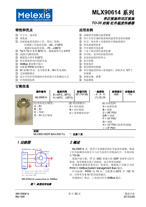
MLX90614 connection to SMBus
图 1: 典型应用电路
2 概述
MLX90614 是一款用于非接触式的红外温度传感器,集成 了红外探测热电堆芯片与信号处理专用集成芯片,全部封装 在 TO-39。
低噪声放大器、17 位 ADC 和强大的 DSP 处理单元的全 集成,使传感器实现了高精度,高分辨率的测量。
- 1、下载文档前请自行甄别文档内容的完整性,平台不提供额外的编辑、内容补充、找答案等附加服务。
- 2、"仅部分预览"的文档,不可在线预览部分如存在完整性等问题,可反馈申请退款(可完整预览的文档不适用该条件!)。
- 3、如文档侵犯您的权益,请联系客服反馈,我们会尽快为您处理(人工客服工作时间:9:00-18:30)。
TION KIT EVALUA BLE A IL A AV
Automotive, Two-Channel Proximity and Touch Sensor
General Description Features
S Low Average Operating Current (100µA at 14V) S 1.2.fF LSB Capacitance-to-Digital Resolution (5pF
Susceptibility and Emissions
S Active-Guard-Sense Architecture Provides
Increased Flexibility in System Packaging
S CMOS/LVCMOS-Compatible Outputs S Embedded µC Supports User-Specified Adaptive
MAX1441
The MAX1441 proximity and touch sensor IC is designed for capacitive proximity sensing in automotive passive remote keyless entry (PRKE) and other applications. This device provides signal processing to support two independent touch/proximity sensor channels. The device features two open-drain output pins with highvoltage capability up to 28V, as well as five digital I/Os to indicate sensing events. During manufacturing, JTAG programming uses four digital I/Os. The device uses grounded electrode capacitive sensing to measure capacitance between one of the two sense pins and the ground. A hand approaching a sense electrode attached to these sense pins causes a change in measured capacitance indicating the presence (touch or proximity) of the object. Activeguard outputs shield the sense electrode from unwanted sources without adding parasitic capacitance. Spread-spectrum techniques in the sensor excitation circuit reduce both electromagnetic emissions and susceptibility to interfering signals. In addition, the sensing excitation frequency is programmable from 100kHz to 500kHz in 10kHz steps to avoid interference. The sensor input signals are converted to a 12-bit digital data and are available to an on-chip microcontroller (FC). The device provides independent offset compensation of up to 63pF for each input channel. Each channel can be programmed to 5pF, 10pF, or 20pF full-scale range. The device features an internal MAXQ® microcontroller with 2kword of flash for user programs and 128 bytes of SRAM. This feature provides the ability to implement customized signal processing and discrimination algorithms that optimize performance in the systems. The device offers user-configurable general-purpose digital I/O lines. Power-on-reset (POR) circuitry provides consistent startup of the device, and a watchdog timer ensures long-term reliable operation of the user’s software. The device is available in a 20-pin TSSOP package and is specified over the -40NC to +105NC automotive temperature range.
Note 1: P ackage thermal resistances were obtained using the method described in JEDEC specification JESD51-7, using a fourlayer board. For detailed information on package thermal considerations, refer to /thermal-tutorial.
ABSOLUTE MAXIMUM RATINGS
(VDD = VAA, AGND = DGND, unless otherwise noted.) VBATT to AGND......................................................-0.3V to +45V VAA, VDD to AGND. ..................................................-0.3V to +4V SINPUT1, SINPUT2, AGUD1, AGUD2 to AGND....................................-0.3V to (VAA + 0.3V) RESET, P0._, I.C. to DGND....................... -0.3V to (VDD + 0.3V) AGND to DGND....................................................-0.3V to +0.3V OUT1, OUT2, to AGND..........................................-0.3V to +28V OUT_, P0._, Continuous Output Current. ........................ P 20mA Continuous Power Dissipation (TA = +70NC) Single-Layer PCB 20-Lead TSSOP (derate 11mW/NC above +70NC).......879mW Multilayer PCB 20-Lead TSSOP (derate 13.6mW/NC above +70NC)..1084mW Junction-to-Case Thermal Resistance (BJC) (Note 1) 20-Lead TSSOP......................................................... +20NC/W Junction-to-Ambient Thermal Resistance (BJA) (Note 1) Single-Layer PCB 20-Lead TSSOP......................................................... +91NC/W Multilayer PCB 20-Lead TSSOP...................................................... +73.8NC/W Operating Temperature Range......................... -40NC to +105NC Junction Temperature......................................................+150NC Storage Temperature Range. ............................ -65NC to +150NC Lead Temperature (soldering, 10s).................................+300NC Soldering Temperature (reflow).......................................+260NC
MAXQ is a registered trademark of Maxim Integrated Products, Inc.