LF353 PDF
LF353运放构成振荡电路
LF353运放构成振荡电路振荡电路如图1所示.由带通滤波器和反相放大器组成。
由R2、C2、R1、C1组成的带通滤波器构成放大器的正反馈电路。
当设定R1=R2=R.C1=C2=C时.在频率为fo时带通滤波器的相位为零。
因此.当把运算放大器的反馈电阻R3和R4设定为R3=2R4时.同相放大器的增益为3倍,在fo处的环路增益正好为1倍,电路产生振荡,并正好能维持振荡。
振荡频率可用fo=1/2πRC进行计算.方法如下:1.给定振荡频率fo和电阻R的值,计算电容器C的值。
例如设fo=1000Hz,R=10kΩ,则可以求得C=0.0159μF。
2.给定振荡频率fo和电容C的值,计算电阻R的值。
由于0.0159μF不是电容器的标称值.必须用几个电容器经串并联组合后才能实现,在制作电路时不但成本高,操作起来也很麻烦。
因此可以先确定电容量,再求电阻阻值。
例如此时将电容量设定为C=0.0159μF,即R=1/2πfoC=10.6kΩ。
对于该振荡电路来说即使环路增益只比1倍稍稍小一点点,电路也不会振荡。
所以在设计实际的电路时为了能确保振荡.将R3和R4设定为R3=2.2 R4的关系。
此时可以确保振荡.但又带来振荡会随时间不断增加,最后导致波形顶部被限幅的问题。
为此需在反馈电路中接入稳压二极管对振幅的增加进行限制。
图2是输出电压为2Vrms,振荡频率为1kHz的振荡电路的例子。
电路的输出阻抗为600Ω。
负反馈量减小放大器的环路增益。
振荡电路的谐波失真率约为0.5%,开机后振幅会不断增大,约需5ms才会稳定下来。
这种振荡电路存在振幅会因R1和R2的误差或者C1和C2的误差而变化,这是这种振荡电路的不足之处。
例如在图3的电路中若R=2.2kΩ,将C2从0.015μF变为0.016μF,振荡电路的振幅会以7Vrms变成9.3Vms.这种振荡电路可振荡的频率范围很宽.可以从数赫兹到数百赫兹。
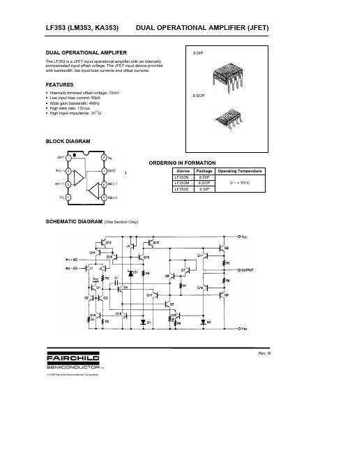
LF353双高阻运算放大器

产品特性● 低功耗● 宽共模(最高为V CC +)、差模电压范围 ● 低输入偏置和失调电流 ● 输出短路保护● 高输入阻抗JFET 输入级 ● 内部频率补偿 ● 无闩锁 ● 高转换速率产品概述该电路为高速JFET 输入双通道运算放大器,单片集成了高匹配、高压JFET 和双极型晶体管。
该器件的特点有高转换速率、低输入偏置和失调电流、低失调电压漂移。
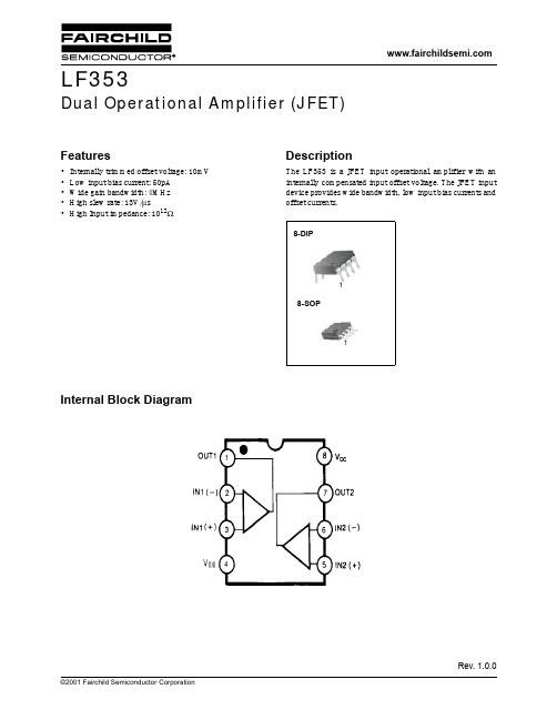
引脚描述(1)金属圆8线 (2)陶瓷双列8线图1 LF353引出端排列(俯视图)电原理图图2 电原理图电参数表表1. LF353电特性,若无其他说明,工作温度为-55℃~+125℃,V CC=±15V。
注1:输入偏置电流是结漏电流,结温每增加10℃,电流值约增加一倍。
绝对最大额定值表2 绝对最大额定值注1:除差模电压外,其他所有电压都是相对于零参考电压(地),即V CC和V CC的中间值。
注2:输入电压的幅度不得超过电源电压和15V二者的较低值。
注3:差分电压是指正相输入端相与反相输入端的电压差。
注4:短路会导致过热和破坏性损耗,各数值为典型值。
注5:输出可能会短路到地或者任一电源,温度或电源电压必须有所限制以保证耗散值不会过大。
应用手册●电压跟随器图3 电压跟随器电路●增益为10的反相放大器图4 增益为10的反相放大器电路封装信息器件采用8引线D型封装和8引线T型封装。
D型封装外形尺寸按GB/T 7092-1993的规定,未注公差的尺寸按GB/T 1804-2000执行,外形尺寸如图5和表3所示。
T型封装外形尺寸按图6和表4的规定。
图5 D型(D08S2)陶瓷双列8线表3 D型(D08S2)封装外形尺寸图6 T型(T08A4)金属圆8线。
LF353中文资料_数据手册_参数
D低输入偏置电流…50 pA型低输入噪声电流0.01 pA/√Hz型低输入噪声电压…18 nV/√Hz型低供电电流…3.6 mA型高输入阻抗…1012年ΩTypD内部削减抵消电压增益带宽……3mhz类型,高转化率…13 V /µs TypdescriptionThis设备是一个低成本、高速、JFET-input运算放大器输入补偿电压很低。
它要求低的供电电流,但LF353保持了一个大的增益带宽产品和快速的转换速度。
此外,调制的高压JFET输入提供非常低的输入偏置和偏置电流。
LF353可用于高速积分器、数模转换器、采样保持电路和许多其他电路。
LF353的特点是在0°C到70°C之间运行。
(每个放大器的输出值+可用选项)包装可用胶带和卷绕。
将后缀R添加到设备类型(即。
LF353DR)。
绝对最大额定参数在操作自由空气的温度范围(除非另外说明)电源电压应用提示(续)由于将输入提高到共模范围内,再次将输入级和放大器置于正常工作模式。
超过单个输入的正共模极限不会改变输出的相位;然而,如果两者都超过了极限,放大器的输出将被迫处于高状态。
放大器的工作将与共模输入电压年龄等于正电源;然而,在这种情况下,增益带宽和旋转速率可能会降低。
当负共模电压荡到负电源的3v以内时,输入偏置伏特可能增加。
每个放大器由齐纳基准分别偏置,允许在±6V功率支持下正常电路运行。
LF353电源电压低于这些可能导致低增益带宽和摆频。
放大器将drivea2kΩ负载电阻±10 v在全温度范围0˚C + 70˚C。
然而,如果放大器被迫驱动更大的负载电流,则可能在负伏特翼上出现输入偏置电压的增加,并最终在正振荡和负振荡上达到有源电流的极限。
LF353应采取措施确保权力supplyfor集成电路不会成为逆转polarityor单位不是无意中安装在asocket向后无限通过resultingforward二极管集成电路中的电流冲击可能导致融合internalconductors和导致破坏单元。
lm353
DUAL OPERATIONAL AMPLIFERThe LF353 is a JFET input operational amplifier with an internally compensated input offset voltage. The JFET input device provides with bandwidth, low input bias currents and offset currents.FEATURES• Internally trimmed offset voltage: 10mV • Low input bias current: 50pA • Wide gain bandwidth: 4MHz • High slew rate: 13V/µs• High Input impedance: 1012ΩBLOCK DIAGRAMORDERING IN FORMATIONiSCHEMATIC DIAGRAM (One Section Only)Device Package Operating TemperatureLF353N 8 DIP LF353M 8 SOP 0 ~ + 70°CLF353S9 SIP©1999 Fairchild Semiconductor CorporationRev. BABSOLUTE MAXIMUM RATINGSELECTRICAL CHARACTERISTICS(V CC =+15V, V EE = -15V, T A =25°C, unless otherwise specified)CharacteristicsSymbol Value Unit Power Supply Voltage Differential Input Voltage Input Voltage Range Output Short Circuit Duration Power DissipationOperating Temperature Range Storage Temperature RangeV CC V I(DIFF)V IP D T OPR T STG ±1830±15Continuous5000 ~ +70-65 ~ +150V V VmW °C °C CharacteristicSymbol Test ConditionsMin Typ Max Unit 5.010°C ≤T A ≤+70°C Input Offset Voltage Drift ∆V IO /∆T R S =10K Ω°C ≤T A ≤+70°C 10 µV/°C 25100pA 0°C ≤T A ≤+70°C4 nA 50200pA 0 °C ≤T A ≤+70°C8nAInput ResistanceR I 1012ΩV O(P-P) = ±0V 25100R L = 2K Ω0°C ≤T A ≤+70°C15 Output Voltage Swing V O(P.P)R L = 10K Ω±12±13.5V Input Voltage RangeV I(R)±11±15/-12V Common Mode Rejection Ratio CMRR R S ≥10K Ω70100dB Power Supply Rejection Ratio PSRR R S ≥10K Ω70100dBPower Supply Current I CC 3.6 6.5mA Slew RateSR G V = 113V/µs Gain-Bandwidth Product GBM 4MHz Channel SeperationCS f = 1Hz ~ 20Khz (Input referenced)120120dB Equivalent Input Noise Voltage V NI R S = 100Ωf = 1KHz 1616nV/√ Equivalent Input Noise CurrentI NIf = 1KHz0.010.01pA/√Hz HzInput Offset Voltage Input Offset Current Input Bias Current Large Signal Voltage Gain G V I BIAS I IO V IO R S =10K ΩV/mV mVTRADEMARKSACEx™CoolFET™CROSSVOLT™E 2CMOS TM FACT™FACT Quiet Series™FAST ®FASTr™GTO™HiSeC™The following are registered and unregistered trademarks Fairchild Semiconductor owns or is authorized to use and is not intended to be an exhaustive list of all such trademarks.LIFE SUPPORT POLICYFAIRCHILD’S PRODUCTS ARE NOT AUTHORIZED FOR USE AS CRITICAL COMPONENTS IN LIFE SUPPORTDEVICES OR SYSTEMS WITHOUT THE EXPRESS WRITTEN APPROV AL OF FAIRCHILD SEMICONDUCTOR CORPORA TION.As used herein:ISOPLANAR™MICROWIRE™POP™PowerTrench™QS™Quiet Series™SuperSOT™-3SuperSOT™-6SuperSOT™-8TinyLogic™1. Life support devices or systems are devices or systems which, (a) are intended for surgical implant intothe body, or (b) support or sustain life, or (c) whosefailure to perform when properly used in accordancewith instructions for use provided in the labeling, can be reasonably expected to result in significant injury to the user.2. A critical component is any component of a lifesupport device or system whose failure to perform can be reasonably expected to cause the failure of the life support device or system, or to affect its safety or effectiveness.PRODUCT STATUS DEFINITIONS Definition of TermsDatasheet Identification Product Status Definition Advance InformationPreliminary No Identification Needed Obsolete This datasheet contains the design specifications for product development. Specifications may change in any manner without notice.This datasheet contains preliminary data, andsupplementary data will be published at a later date.Fairchild Semiconductor reserves the right to make changes at any time without notice in order to improve design.This datasheet contains final specifications. Fairchild Semiconductor reserves the right to make changes at any time without notice in order to improve design.This datasheet contains specifications on a product that has been discontinued by Fairchild semiconductor.The datasheet is printed for reference information only.Formative or In DesignFirst ProductionFull ProductionNot In ProductionDISCLAIMERFAIRCHILD SEMICONDUCTOR RESERVES THE RIGHT TO MAKE CHANGES WITHOUT FURTHER NOTICE TO ANY PRODUCTS HEREIN TO IMPROVE RELIABILITY , FUNCTION OR DESIGN. FAIRCHILD DOES NOT ASSUME ANY LIABILITY ARISING OUT OF THE APPLICATION OR USE OF ANY PRODUCT OR CIRCUIT DESCRIBED HEREIN; NEITHER DOES IT CONVEY ANY LICENSE UNDER ITS PATENT RIGHTS, NOR THE RIGHTS OF OTHERS.。
lf353工作原理
lf353工作原理
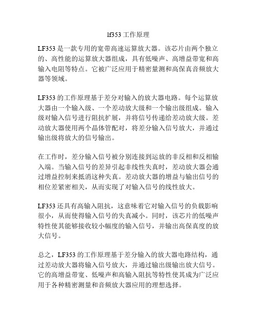
LF353是一款专用的宽带高速运算放大器。
该芯片由两个独立的、高性能的运算放大器组成,具有低噪声、高增益带宽和高输入电阻等特点。
它被广泛应用于精密量测和高保真音频放大器等领域。
LF353的工作原理基于差分对输入的放大器电路。
每个运算放大器由一个输入级、一个差动放大级和一个输出级组成。
输入级对输入信号进行阻抗扩展,并将信号传递给差动放大级。
差动放大器使用两个晶体管配对,将差分输入信号放大,并通过输出级将放大的信号输出。
在工作时,差分输入信号被分别连接到运放的非反相和反相输入端。
当输入信号的差异引起非线性失真时,差动放大器会通过增益控制来抵消这种失真。
差动放大器的增益与输出信号的相位差紧密相关,从而实现了对输入信号的线性放大。
LF353还具有高输入阻抗,这意味着它对输入信号的负载影响很小,从而使得输入信号的失真减小。
同时,该芯片的低噪声特性使其能够接收较小幅度的输入信号,并输出高保真度的放大信号。
总之,LF353的工作原理基于差分输入的放大器电路结构,通过差动放大器将输入信号放大,并通过输出级输出放大信号。
它的高增益带宽、低噪声和高输入阻抗等特性使其成为广泛应用于各种精密测量和音频放大器应用的理想选择。
LF353N_NL中文资料
©2001 Fairchild Semiconductor CorporationRev. 1.0.0Features•Internally trimmed offset voltage: 10mV •Low input bias current: 50pA •Wide gain bandwidth: 4MHz •High slew rate: 13V/µs•High Input impedance: 1012ΩDescriptionThe LF353 is a JFET input operational amplifier with an internally compensated input offset voltage. The JFET input device provides wide bandwidth, low input bias currents and offset currents.8-DIP18-SOP1Internal Block DiagramLF353Dual Operational Amplifier (JFET)LF3532Schematic Diagram(One Section Only)Absolute Maximum RatingsParameterSymbol Value UnitPower Supply Voltage V CC ±18V Differential Input Voltage V I(DIFF)30V Input Voltage Range V I ±15V Output Short Circuit Duration -Continuous-Power DissipationP D 500mW Operating Temperature Range T OPR 0 ~ +70°C Storage Temperature RangeT STG-65 ~ +150°CLF3533Electrical Characteristics(V CC =+15V, V EE = -15V, T A =25 °C, unless otherwise specified)ParameterSymbol ConditionsMin.Typ.Max.Unit Input Offset Voltage V IOR S =10K Ω- 5.010mV 0 °C ≤T A ≤+70 °C ----Input Offset Voltage Drift ∆V IO /∆T R S =10K Ω0 °C ≤T A ≤+70 °C -10- µV/ °C Input Offset Current I IO -25100pA 0 °C ≤T A ≤+70 °C --4 nA Input Bias Current I BIAS -50200pA 0 °C ≤T A ≤+70 °C --8 nAInput ResistanceR I --1012-ΩLarge Signal Voltage Gain G VV O(P-P) = ±10V 25100-V/mV R L = 2K Ω0 °C ≤T A ≤+70 °C 15---Output Voltage Swing V O(P_P)R L = 10K Ω±12±13.5-V Input Voltage RangeV I(R)-±11±15/-12-V Common Mode Rejection Ratio CMRR R S ≤ 10K Ω70100-dB Power Supply Rejection Ratio PSRR R S ≤ 10K Ω70100-dB Power Supply Current I CC -- 3.6 6.5mA Slew RateSR G V = 1-13-V/µS Gain-Bandwidth Product GBW --4-MHz Channel SeperationCS f = 1Hz ~ 20KHz (Input referenced)-120-dB Equivalent Input Noise Voltage V NI R S = 100Ωf = 1KHz -16- nV/Equivalent Input Noise CurrentI NIf = 1KHz-0.01- pA/HzHzLF353Mechanical DimensionsPackage8-DIP4LF353 Mechanical DimensionsPackage8-SOP5LF3536/1/01 0.0m 001Stock#DSxxxxxxxx2001 Fairchild Semiconductor CorporationLIFE SUPPORT POLICYFAIRCHILD’S PRODUCTS ARE NOT AUTHORIZED FOR USE AS CRITICAL COMPONENTS IN LIFE SUPPORT DEVICES OR SYSTEMS WITHOUT THE EXPRESS WRITTEN APPROVAL OF THE PRESIDENT OF FAIRCHILD SEMICONDUCTOR CORPORATION. As used herein:1.Life support devices or systems are devices or systemswhich, (a) are intended for surgical implant into the body, or (b) support or sustain life, and (c) whose failure to perform when properly used in accordance with instructions for use provided in the labeling, can bereasonably expected to result in a significant injury of the user.2. A critical component in any component of a life supportdevice or system whose failure to perform can bereasonably expected to cause the failure of the life support device or system, or to affect its safety or effectiveness.DISCLAIMERFAIRCHILD SEMICONDUCTOR RESERVES THE RIGHT TO MAKE CHANGES WITHOUT FURTHER NOTICE TO ANY PRODUCTS HEREIN TO IMPROVE RELIABILITY, FUNCTION OR DESIGN. FAIRCHILD DOES NOT ASSUME ANYLIABILITY ARISING OUT OF THE APPLICATION OR USE OF ANY PRODUCT OR CIRCUIT DESCRIBED HEREIN; NEITHER DOES IT CONVEY ANY LICENSE UNDER ITS PATENT RIGHTS, NOR THE RIGHTS OF OTHERS.Ordering InformationProduct NumberPackage Operating TemperatureLF353N 8-DIP 0 ~ + 70°CLF353M8-SOP。
lf353芯片资料

PACKAGING INFORMATION Orderable DeviceStatus (1)Package Type Package Drawing Pins Package Qty Eco Plan (2)Lead/Ball Finish MSL Peak Temp (3)LF353DACTIVE SOIC D 875Green (RoHS &no Sb/Br)CU NIPDAU Level-1-260C-UNLIM LF353DE4ACTIVE SOIC D 875Green (RoHS &no Sb/Br)CU NIPDAU Level-1-260C-UNLIM LF353DG4ACTIVE SOIC D 875Green (RoHS &no Sb/Br)CU NIPDAU Level-1-260C-UNLIM LF353DRACTIVE SOIC D 82500Green (RoHS &no Sb/Br)CU NIPDAU Level-1-260C-UNLIM LF353DRE4ACTIVE SOIC D 82500Green (RoHS &no Sb/Br)CU NIPDAU Level-1-260C-UNLIM LF353DRG4ACTIVE SOIC D 82500Green (RoHS &no Sb/Br)CU NIPDAU Level-1-260C-UNLIM LF353PACTIVE PDIP P 850Pb-Free (RoHS)CU NIPDAU N /A for Pkg Type LF353PE4ACTIVE PDIP P 850Pb-Free (RoHS)CU NIPDAU N /A for Pkg Type (1)The marketing status values are defined as follows:ACTIVE:Product device recommended for new designs.LIFEBUY:TI has announced that the device will be discontinued,and a lifetime-buy period is in effect.NRND:Not recommended for new designs.Device is in production to support existing customers,but TI does not recommend using this part in a new design.PREVIEW:Device has been announced but is not in production.Samples may or may not be available.OBSOLETE:TI has discontinued the production of the device.(2)Eco Plan -The planned eco-friendly classification:Pb-Free (RoHS),Pb-Free (RoHS Exempt),or Green (RoHS &no Sb/Br)-please check /productcontent for the latest availability information and additional product content details.TBD:The Pb-Free/Green conversion plan has not been defined.Pb-Free (RoHS):TI's terms "Lead-Free"or "Pb-Free"mean semiconductor products that are compatible with the current RoHS requirements for all 6substances,including the requirement that lead not exceed 0.1%by weight in homogeneous materials.Where designed to be soldered at high temperatures,TI Pb-Free products are suitable for use in specified lead-free processes.Pb-Free (RoHS Exempt):This component has a RoHS exemption for either 1)lead-based flip-chip solder bumps used between the die and package,or 2)lead-based die adhesive used between the die and leadframe.The component is otherwiseconsidered Pb-Free (RoHS compatible)as defined above.Green (RoHS &no Sb/Br):TI defines "Green"to mean Pb-Free (RoHS compatible),and free of Bromine (Br)and Antimony (Sb)based flame retardants (Br or Sb do not exceed 0.1%by weight in homogeneous material)(3)MSL,Peak Temp.--The Moisture Sensitivity Level rating according to the JEDEC industry standard classifications,and peak solder temperature.Important Information and Disclaimer:The information provided on this page represents TI's knowledge and belief as of the date that it is provided.TI bases its knowledge and belief on information provided by third parties,and makes no representation or warranty as to the accuracy of such information.Efforts are underway to better integrate information from third parties.TI has taken and continues to take reasonable steps to provide representative and accurate information but may not have conducted destructive testing or chemical analysis on incoming materials and chemicals.TI and TI suppliers consider certain information to be proprietary,and thus CAS numbers and other limited information may not be available for release.In no event shall TI's liability arising out of such information exceed the total purchase price of the TI part(s)at issue in this document sold by TI to Customer on an annual basis.PACKAGE OPTION ADDENDUM 24-Oct-2006TAPE AND REEL INFORMATION*All dimensions are nominal Device Package Type Package DrawingPinsSPQ Reel Diameter (mm)Reel Width W1(mm)A0(mm)B0(mm)K0(mm)P1(mm)W (mm)Pin1Quadrant LF353DR SOICD 82500330.012.4 6.4 5.2 2.18.012.0Q1LF353DR SOIC D 82500330.012.4 6.4 5.2 2.18.012.0Q1*All dimensions are nominalDevice Package Type Package Drawing Pins SPQ Length(mm)Width(mm)Height(mm) LF353DR SOIC D8*******.5338.120.6LF353DR SOIC D8*******.0346.029.0IMPORTANT NOTICETexas Instruments Incorporated and its subsidiaries(TI)reserve the right to make corrections,modifications,enhancements,improvements, and other changes to its products and services at any time and to discontinue any product or service without notice.Customers should obtain the latest relevant information before placing orders and should verify that such information is current and complete.All products are sold subject to TI’s terms and conditions of sale supplied at the time of order acknowledgment.TI warrants performance of its hardware products to the specifications applicable at the time of sale in accordance with TI’s standard warranty.Testing and other quality control techniques are used to the extent TI deems necessary to support this warranty.Except where mandated by government requirements,testing of all parameters of each product is not necessarily performed.TI assumes no liability for applications assistance or customer product design.Customers are responsible for their products and applications using TI components.To minimize the risks associated with customer products and applications,customers should provide adequate design and operating safeguards.TI does not warrant or represent that any license,either express or implied,is granted under any TI patent right,copyright,mask work right, or other TI intellectual property right relating to any combination,machine,or process in which TI products or services are rmation published by TI regarding third-party products or services does not constitute a license from TI to use such products or services or a warranty or endorsement e of such information may require a license from a third party under the patents or other intellectual property of the third party,or a license from TI under the patents or other intellectual property of TI.Reproduction of TI information in TI data books or data sheets is permissible only if reproduction is without alteration and is accompanied by all associated warranties,conditions,limitations,and notices.Reproduction of this information with alteration is an unfair and deceptive business practice.TI is not responsible or liable for such altered rmation of third parties may be subject to additional restrictions.Resale of TI products or services with statements different from or beyond the parameters stated by TI for that product or service voids all express and any implied warranties for the associated TI product or service and is an unfair and deceptive business practice.TI is not responsible or liable for any such statements.TI products are not authorized for use in safety-critical applications(such as life support)where a failure of the TI product would reasonably be expected to cause severe personal injury or death,unless officers of the parties have executed an agreement specifically governing such use.Buyers represent that they have all necessary expertise in the safety and regulatory ramifications of their applications,and acknowledge and agree that they are solely responsible for all legal,regulatory and safety-related requirements concerning their products and any use of TI products in such safety-critical applications,notwithstanding any applications-related information or support that may be provided by TI.Further,Buyers must fully indemnify TI and its representatives against any damages arising out of the use of TI products in such safety-critical applications.TI products are neither designed nor intended for use in military/aerospace applications or environments unless the TI products are specifically designated by TI as military-grade or"enhanced plastic."Only products designated by TI as military-grade meet military specifications.Buyers acknowledge and agree that any such use of TI products which TI has not designated as military-grade is solely at the Buyer's risk,and that they are solely responsible for compliance with all legal and regulatory requirements in connection with such use. TI products are neither designed nor intended for use in automotive applications or environments unless the specific TI products are designated by TI as compliant with ISO/TS16949requirements.Buyers acknowledge and agree that,if they use any non-designated products in automotive applications,TI will not be responsible for any failure to meet such requirements.Following are URLs where you can obtain information on other Texas Instruments products and application solutions:Products ApplicationsAudio /audio Automotive and Transportation /automotiveAmplifiers Communications and Telecom /communicationsData Converters Computers and Peripherals /computersDLP®Products Consumer Electronics /consumer-appsDSP Energy and Lighting /energyClocks and Timers /clocks Industrial /industrialInterface Medical /medicalLogic Security /securityPower Mgmt Space,Avionics and Defense /space-avionics-defense Microcontrollers Video and Imaging /videoRFID OMAP Mobile Processors /omapWireless Connectivity /wirelessconnectivityTI E2E Community Home Page Mailing Address:Texas Instruments,Post Office Box655303,Dallas,Texas75265Copyright©2012,Texas Instruments Incorporated。
运放大全

LFC2 高增益运算放大器LFC3 中增益运算放大器LFC4 低功耗运算放大器LFC54 低功耗运算放大器LFC75 低功耗运算放大器F003 通用Ⅱ型运算放大器F004(5G23) 中增益运算放大器F005 中增益运算放大器F006 通用Ⅱ型运算放大器F007(5G24) 通用Ⅲ型运算放大器 F010 低功耗运算放大器F011 低功耗运算放大器F1550 射频放大器F1490 宽频带放大器F1590 宽频带放大器F157/A 通用型运算放大器F253 低功耗运算放大器F741(F007) 通用Ⅲ型运算放大器 F741A 通用型运算放大器F747 双运算放大器OP-07 超低失调运算放大器OP111A 低噪声运算放大器F4741 通用型四运算放大器F101A/201A 通用型运算放大器 F301A 通用型运算放大器F108 通用型运算放大器F308 通用型运算放大器F110/210 电压跟随器F310 电压跟随器F118/218 高速运算放大器F441 低功耗JEET输入运算放大器 F318 高速运算放大器F124/224 四运算放大器F324 四运算放大器F148 通用型四运算放大器F248/348 通用型四运算放大器F158/258 单电源双运算放大器F358 单电源双运算放大器F1558 通用型双运算放大器F4558 双运算放大器LF791 单块集成功率运算放大器 LF4136 高性能四运算放大器FD46 高速运送放大器LF082 高输入阻抗运送放大器LFOP37 超低噪声精密放大器LF3140 高输入阻抗双运送放大器LF7650 斩波自稳零运送放大器LZ1606 积分放大器LZ19001 挠性石英表伺服电路变换放大器 LBMZ1901 热电偶温度变换器LM741 运算放大器LM747 双运算放大器OP-07 超低失调运算放大器LM101/201 通用型运算放大器LM301 通用型运算放大器LM108/208 通用型运算放大器LM308 通用型运算放大器LM110 电压跟随器LM310 电压跟随器LM118/218 高速运算放大器LM318 高速运算放大器LM124/224 四运算放大器LM324 四运算放大器LM148 四741运算放大器LM248/348 四741运算放大器LM158/258 单电源双运算放大器LM358 单电源双运算放大器LM1558 双运算放大器OP-27CP 低噪声运算放大器TL062 低功耗JEET运算放大器TL072 低噪声JEET输入型运算放大器TL081 通用JEET输入型运算放大器TL082 四高阻运算放大器(JEET)TL084 四高阻运算放大器(JEET)MC1458 双运放(内补偿)LF147/347 JEET输入型运算放大器LF156/256/356 JEET输入型运算放大器 LF107/307 运算放大器LF351 宽带运算放大器LF353 双高阻运算放大器LF155/355 JEET输入型运算放大器LF157/357 JEET输入型运算放大器LM359 双运放(GB=400MC)LM381 双前置放大器CA3100 宽频带运算放大器CA3130 BiMOS运算放大器CA3140 BiMOS运算放大器CA3240 BiMOS双运算放大器CA3193 BiMOS精密运算放大器CA3401 单电源运算放大器MC3303 单电源四运算放大器MC3403 低功耗四运放LF411 低失调低漂移JEET输入运放LF444 四高阻抗运算放大器μpc4558 低噪声宽频带运放MC4741 四通用运放LM709 通用运放LM725 低漂移高精度运放LM733 宽带放大器LM748 双运放ICL7650 斩波稳零运放ICL7660 CMOS电压放大(变换)器=============常见运放型号简介CA3130 高输入阻抗运算放大器 Intersil[DATA]CA3140 高输入阻抗运算放大器CD4573 四可编程运算放大器 MC14573ICL7650 斩波稳零放大器LF347(NS[DATA]) 带宽四运算放大器 KA347LF351 BI-FET单运算放大器 NS[DATA]LF353 BI-FET双运算放大器 NS[DATA]LF356 BI-FET单运算放大器 NS[DATA]LF357 BI-FET单运算放大器 NS[DATA]LF398 采样保持放大器 NS[DATA]LF411 BI-FET单运算放大器 NS[DATA]LF412 BI-FET双运放大器 NS[DATA]LM124 低功耗四运算放大器(军用档) NS[DATA]/TI[DATA] LM1458 双运算放大器 NS[DATA]LM148 四运算放大器 NS[DATA]LM224J 低功耗四运算放大器(工业档) NS[DATA]/TI[DATA] LM2902 四运算放大器 NS[DATA]/TI[DATA]LM2904 双运放大器 NS[DATA]/TI[DATA]LM301 运算放大器 NS[DATA]LM308 运算放大器 NS[DATA]LM308H 运算放大器(金属封装) NS[DATA]LM318 高速运算放大器 NS[DATA]LM324(NS[DATA]) 四运算放大器 HA17324,/LM324N(TI)LM348 四运算放大器 NS[DATA]LM358 NS[DATA] 通用型双运算放大器 HA17358/LM358P(TI) LM380 音频功率放大器 NS[DATA]LM386-1 NS[DATA] 音频放大器 NJM386D,UTC386LM386-3 音频放大器 NS[DATA]LM386-4 音频放大器 NS[DATA]LM3886 音频大功率放大器 NS[DATA]LM3900 四运算放大器LM725 高精度运算放大器 NS[DATA]LM733 带宽运算放大器LM741 NS[DATA] 通用型运算放大器 HA17741MC34119 小功率音频放大器NE5532 高速低噪声双运算放大器 TI[DATA]NE5534 高速低噪声单运算放大器 TI[DATA]NE592 视频放大器OP07-CP 精密运算放大器 TI[DATA]OP07-DP 精密运算放大器 TI[DATA]TBA820M 小功率音频放大器 ST[DATA]TL061 BI-FET单运算放大器 TI[DATA]TL062 BI-FET双运算放大器 TI[DATA]TL064 BI-FET四运算放大器 TI[DATA]TL072 BI-FET双运算放大器 TI[DATA]TL074 BI-FET四运算放大器 TI[DATA]TL081 BI-FET单运算放大器 TI[DATA]TL082 BI-FET双运算放大器 TI[DATA]。
- 1、下载文档前请自行甄别文档内容的完整性,平台不提供额外的编辑、内容补充、找答案等附加服务。
- 2、"仅部分预览"的文档,不可在线预览部分如存在完整性等问题,可反馈申请退款(可完整预览的文档不适用该条件!)。
- 3、如文档侵犯您的权益,请联系客服反馈,我们会尽快为您处理(人工客服工作时间:9:00-18:30)。
Industrial Temperature Range (– 25°C to +85°C) LM201A 0.075 2.0 10 10 50 1.0 0.5 General Purpose N/626, D/751
Internally Compensated
Commercial Temperature Range (0°C to +70°C) LF351 LF411C MC1436, C MC1741C MC1776C MC3476 MC34001 MC34001B MC34071 MC34071A MC34080B MC34081B MC34181 TL071AC TL071C TL081AC TL081C 200 pA 200 pA 0.04 0.5 0.003 0.05 200 pA 200 pA 0.5 500 nA 200 pA 200 pA 0.1 nA 200 pA 200 pA 200 pA 400 pA 10 2.0 10 6.0 6.0 6.0 10 5.0 5.0 3.0 1.0 1.0 2.0 6.0 10 6.0 15 10 10 12 15 15 15 10 10 10 10 10 10 10 10 10 10 10 100 pA 100 pA 10 200 3.0 25 100 pA 100 pA 75 50 100 pA 100 pA 0.05 50 pA 50 pA 100 pA 200 pA 25 25 70 20 100 50 25 50 25 50 25 25 25 50 25 50 25 4.0 8.0 1.0 1.0 1.0 1.0 4.0 4.0 4.5 4.5 16 8.0 4.0 4.0 4.0 4.0 4.0 13 25 2.0 0.5 0.2 0.2 13 13 10 10 55 30 10 13 13 13 13 ±5.0 +5.0 ±15 ±3.0 ±1.2 ±1.5 ±5.0 ±5.0 +3.0 +3.0 ±5.0 ±5.0 ±2.5 ±5.0 ±5.0 ±5.0 ±5.0 ±18 ±22 ±34 ±18 ±18 ±18 ±18 ±18 +44 +44 ±22 ±22 ±18 ±18 ±18 ±18 ±18 JFET Input JFET Input, Low Offset, Low Drift High Voltage General Purpose µPower, Programmable Low Cost, µPower, Programmable JFET Input JFET Input High Performance Single Supply Decompensated High Speed, JFET Input Low Power, JFET Input Low Noise, JFET Input Low Noise, JFET Input JFET Input JFET Input N/626, D/751 N/626, D/751 P1/626, D/751 P1/626, D/751 P1/626, D/751 P1/626 P/626, D/751 P/626, D/751 P/626, D/751 P/626, D/751 P/626, D/751 P/626, D/751 P/626 P/626 D/751 P/626 D/751
Motorola Master Selection Guide
4.1–1
Analog and Interface Integrated Circuits
Operational Amplifiers
Motorola offers a broad line of bipolar operational amplifiers to meet a wide range of applications. From low–cost industry–standard types to high precision circuits, the span encompasses a large range of performance capabilities. These Analog integrated circuits are available as single, dual and quad monolithic devices in a variety of temperature ranges and package ห้องสมุดไป่ตู้tyles. Most devices may be obtained in unencapsulated ‘‘chip’’ form as well. For price and delivery information on chips, please contact your Motorola Sales Representative or Distributor.
Amplifiers and Comparators
In Brief . . .
For over two decades, Motorola has continually refined and updated integrated circuit technologies, analog circuit design techniques and processes in response to the needs of the marketplace. The enhanced performance of newer operational amplifiers and comparators has come through innovative application of these technologies, designs and processes. Some early designs are still available but are giving way to the new, higher performance operational amplifier and comparator circuits. Motorola has pioneered in JFET inputs, low temperature coefficient input stages, Miller loop compensation, all NPN output stages, dual–doublet frequency compensation and analog “in–the–package” trimming of resistors to produce superior high performance operational amplifiers and comparators, operating in many cases from a single supply with low input offset, low noise, low power, high output swing, high slew rate and high gain–bandwidth product at reasonable cost to the customer. Present day operational amplifiers and comparators find applications in all market segments including motor controls, instrumentation, aerospace, automotive, telecommunications, medical, and consumer products. Page Operational Amplifiers . . . . . . . . . . . . . . . . . . . . . . . . . . . 4.1–2 Single . . . . . . . . . . . . . . . . . . . . . . . . . . . . . . . . . . . . . . 4.1–2 Dual . . . . . . . . . . . . . . . . . . . . . . . . . . . . . . . . . . . . . . . 4.1–3 Quad . . . . . . . . . . . . . . . . . . . . . . . . . . . . . . . . . . . . . . . 4.1–4 One Volt SMARTMOS™ Rail–to–Rail Dual Operational Amplifier . . . . . . . . . . . . . . . . . . . . . . . . . . . 4.1–6 High Frequency Amplifiers . . . . . . . . . . . . . . . . . . . . . . . 4.1–7 AGC . . . . . . . . . . . . . . . . . . . . . . . . . . . . . . . . . . . . . . . 4.1–7 Miscellaneous Amplifiers . . . . . . . . . . . . . . . . . . . . . . . . 4.1–8 Bipolar . . . . . . . . . . . . . . . . . . . . . . . . . . . . . . . . . . . . . 4.1–8 CMOS . . . . . . . . . . . . . . . . . . . . . . . . . . . . . . . . . . . . . 4.1–8 Comparators . . . . . . . . . . . . . . . . . . . . . . . . . . . . . . . . . . . 4.1–9 Single . . . . . . . . . . . . . . . . . . . . . . . . . . . . . . . . . . . . . . 4.1–9 Dual . . . . . . . . . . . . . . . . . . . . . . . . . . . . . . . . . . . . . . . 4.1–9 Quad . . . . . . . . . . . . . . . . . . . . . . . . . . . . . . . . . . . . . . . 4.1–9 Package Overview . . . . . . . . . . . . . . . . . . . . . . . . . . . . 4.1–10