2、SG6841原理和易损元件
SG6841D电路图

Bb s .C hi n ad z.C omOPERATION DESCRIPTION Start-up currentTypical start-up current is only 30uA so that a high resistance, and low-wattage, start-up resistor can be used to minimize power loss. For an AC/DC adapter with universal input range, a 1.5 M Ω, 0.25W, start-up resistor and a 10uF/25V VDD hold-up capacitor are enough for this application.Operating currentOperating current has been reduced to 3mA. The low operating current enables a better efficiency and reduces the requirement of VDD hold-up capacitance.Green Mode OperationThe patented green-mode function provides an off-time modulation to reduce the switching frequency in the light load and no load conditions. The on time is limited for better abnormal or brownout protection. V FB , which is derived from the voltage feedback loop, is taken as the reference. Once V FB is lower than the threshold voltage, switching frequency will be linearly decreased to the minimum green mode frequency around 10kHz (R i =26k Ω).Oscillator OperationA resistor from RI pin to ground will generate a constant current source for SG6841. This current is used to charge an internal capacitor and hence the internal clock and switching frequency are determined. Increase the resistance will decrease the current source and reduce the switching frequency. A 26k Ω resistor R i creates a 50uA constant current I i and generates 65kHz switching frequency. The relation between Ri and switching freauency is:)(kHz )(k R 1690 I PWM f Ω=---------------------------- (1)The range of the PWM oscillation frequency is designed as 50kHz ~ 90kHz.Current sensing and PWM current limitingPeak current mode control is utilized in SG6841 to regulate output voltage and provide pulse by pulse current limiting. The switch current is detected by a sense resistor into the sense pin of SG6841. The PWM duty cycle is determined by this current sense signal and V FB , the feedback voltage. When the voltage on sense pin reaches V COMP = (V FB –1.0)/3, a switch cycle will be terminated immediately. V COMP is internally clamped to a variable voltage around 0.85v for output power limit.Leading Edge BlankingEach time when the power MOSFET is switched on,a turn-on spike will inevitably occur on the sense-resistor. To avoid premature termination of the switching pulse, a 270 nsec leading-edge blanking time is built in. Conventional RC filtering can therefore be omitted. During this blanking period, the current-limit comparator is disabled and it cannot switch off the gate driver.Under-voltage lockout (UVLO)The turn-on and turn-off threshold of SG6841 arefixed internally at 16V/10V. During start-up, the hold-up capacitor must be charged to 16V through the start-up resistor so that SG6841 will be enabled. The hold-up capacitor will continue to supply V DD before the energy can be delivered from auxiliary winding of the main transformer. V DD must not drop below 10V during this start-up process. This UVLO hysteresis window insures that hold-up capacitor is adequate to supply V DD during start-up.Gate Output / Soft DrivingThe SG6841 BiCMOS output stage is a fast totem pole gate driver. Cross conduction has been avoided to minimize heat dissipation, increases efficiency and enhances reliability. The output driver is clamped by an internal 18V Zener diode in order to protect power MOSFET transistors against undesirable gate over voltage. A soft driving waveform is implemented to minimize EMI.B b s.Ch i na dz.Co mBuilt-in Slope CompensationThe sensed voltage across the current sense resistor is used for current mode control and pulse-by-pulse current limiting. Built-in slope compensation will improve stability or prevent sub-harmonic oscillation of peak current mode control. SG6841 inserts a synchronized positive-going ramp at every switching cycle. Vs-comp = 0.33V.Constant Output Power LimitWhen the SENSE voltage, across the sense resistor Rs, reaches the threshold voltage, around 1.0V, the output GATE drive will be turned off after a small propagation delay t D. This propagation delay will introduce an additional current proportional to t D*Vin/Lp. Since the propagation delay is nearly constant regardless of the input line voltage V IN. Higher input line voltage will result in a larger additional current and hence the output power limit is also higher than that under low input line voltage. To compensate this variation for wide AC input range, the threshold voltage is adjusted by the V IN current. Since VIN pin is connected to the rectified input line voltage through the start-up resistor, a higher line voltage will generate higher V IN current into the VIN pin. The threshold voltage is decreased if the V IN current is increased. Smaller threshold voltage, forces the output GATE drive to terminate earlier, thus reduce the total PWM turn-on time and make the output power equal to that of low line input. This proprietary internal compensation ensures a constant output power limit for wide AC input voltage from 90VAC to 264VAC.Thermal ProtectionAn NTC thermistor Rntc in series with a resistor Ra can be connected from pin RT to ground. A constant current I RT is output from pin RT. The voltage on RT pin can be expressed as V RT = I RT × (Rntc + Ra) in which I RT = 2 x (1.3V / Ri).At high ambient temperature, Rntc will be smaller such that V RT will decrease. When V RT is less than 0.65V (V OTP,START), the PWM duty cycle will be decreased to lower the internal temperature of power supply. If the over heating situation still exists such that V RT decreases further to 0.62V (V OTP,STOP), the PWM will be completely turned off.Limited Power ControlEvery time when the output of power supply is shorted or over loaded, the FB voltage will increase. If the FB voltage is higher than a designed threshold, 4.2V, for longer than 31msec, the PWM output will then be turned off eternally. V DD, the supply voltage for SG6841, will decrease due to the supply current for SG6841. When V DD is lower than the turn-off threshold such as 10V, SG6841 will be totally shut down. Due to the start up resistor, V DD will be charged up to the turn-on threshold voltage 16V until SG6841 is enabled again. If the over loading condition still exists, above protection will take place repeatedly. This will prevent the power supply from being overheated under over loading condition.Noise immunityNoise on the current sense or control signal may cause significant pulse width jitter, particularly in the continuous conduction mode. Slope compensation helps alleviate this problem. Good placement and layout practices should be followed. Avoiding long PCB traces and component leads, locating compensation and filter components near to the SG6841, and increasing the power MOS gate resistance will always help.B b s.Ch i na dz.Co m DISCLAIMERSLIFE SUPPORTSystem General’s products are not designed to be used as components in devices intended to support or sustain human life. Use of System General’s products in components intended for surgical implant into the body, or other applications in which failure of the System General’s products could create a situation where personal death or injury may occur, is not authorized without the express written approval of System General’s Chief Executive Officer. System General will not be held liable for any damages or claims resulting from the use of its products in medical applications. MILITARYSystem General's products are not designed for use in military applications. Use of System General’s products in military applications is not authorized without the express written approval of System General’s Chief Executive Officer. System General will not be held liable for any damages or claims resulting from the use of its products in military applications.RIGHT TO MAKE CHANGESSystem General reserves the right to change this document and/or this product without notice. Customers are advised to consult their System General sales representative before ordering.。
PCS-9662辅助装置技术说明书(20141202)
南京南瑞继保电气有限公司
iii
PCS-9662 辅助装置
目录
前言 .......................................................................................................................................i 目录 .....................................................................................................................................iv 第 1 章 概述........................................................................................................................1
危险!
意味着如果安全预防措施被忽视,则会导致人员死亡, 严重的人身伤害,或严重的设备 损坏。
警告!
意味着如果安全预防措施被忽视,则可能导致人员死亡, 严重的人身伤害,或严重的设 备损坏。
警示!
意味着如果安全预防措施被忽视,则可能导致轻微的人身伤害或设备损坏。本条特别适 用于对装置的损坏及可能对被保护设备的损坏。
2.1.1 直流电源.......................................................................................................3 2.2 机械结构 .................................................................................................................3 2.3 环境条件参数..........................................................................................................3 2.4 型式试验 .................................................................................................................3
基于SG6841LCD显示器开关电源故障检测与维修

基于SG6841LCD显示器开关电源故障检测与维修摘要:由SG6841开关电源驱动器件构成的LCD显示器开关电源由于工作在高频、高电压启动以及输出大电流的状态下,极易发生故障。
该文结合SG6841构成开关电源电路的工作原理,分析和总结基于SG6841 LCD显示器开关电源故障检测的方法和技巧。
关键词:LCD;脉宽调制;开关电源;检测;技法Fault Detection and Maintenance of The LCD Display‘s Switching Power Based on SG6841GAO Zi-li(Xuzhou Radio TV University, Xuzhou 221006, China)Abstract: The LCD Display‘s switching power which is made up of SG6841 switching power driver is easily to break down when it works in a state of high frequency, high voltage boot or heavy current output. This article combines the working principle of the switching power circuit which formed by SG6841 and analyses and summarizes the fault detection and maintenance of the LCD display‘s switching power based on SG6841.Key words: LCD; pulse width modulation(PWM); switching power; detection; technical skillSG6841是一款高性能固定频率电流模式控制器,属于电流型单端PWM调制器,具有外围电路简单、性能优良、电压调整率好等优点,广泛应用于LCD显示器等电子设备中作开关电源驱动器件。
艾默生UPS用户手册
警告
大对地漏电流:在接入输入电源前(包括交流市电和电池),请务必可靠接地。 设备的接地必须符合当地电气规程。
UPS 系统前级配电保护设备的选择必须符合当地电气规程。
警告
警告 UPS 内部保险损坏,更换时必须使用相同电气参数的保险,并由专业人员操作。
小心
本设备安装有射频干扰(RFI)滤波器。 对地漏电流在 3.5 mA~1000mA 之间。 在选择瞬变漏电流断路器(RCCB)或其它漏电检测仪器(RCD)时应考虑设备启动时可能出现的瞬态和稳态对地漏电流。 必须选择对单向直流脉冲(A 级)和瞬态电流脉冲不敏感的 RCCB。 请注意负载的对地漏电流也将流过 RCCB 或 RCD。
型号 UF-BCB500/0500-03、UF-BCB300/0500-03 TMP12Z UF-SNMP114 UF-MODBUS110 UF-DRY210 UF-DRYCONTACTOR UF-BATTLEAK
UF-DRY110 SPD24Z-SPD-24
-
安全事项
遵守及标准
本设备符合以下 UPS 参考标准: z IEC60950-1,IEC62040-1-1 使用操作区一般安全要求 z IEC/EN62040-2 EMC 要求 z IEC62040-3 性能要求和测试方法
1.1 特点.........................................................................................................................................................................................1 1.2 设计思想.................................................................................................................................................................................1
SG6841
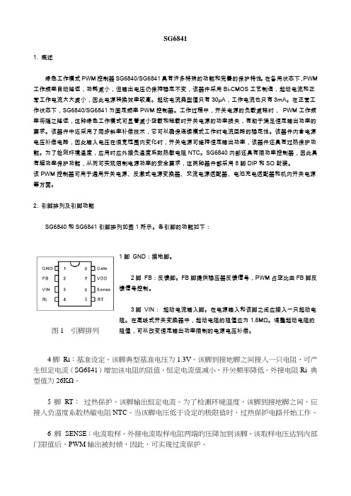
SG68411. 概述绿色工作模式PWM控制器SG6840/SG6841具有许多特殊的功能和完善的保护特性。
在备用状态下,PWM 工作频率自动降低,功耗减小,但输出电压仍保持稳定不变,该器件采用Bi-CMOS工艺制造,起动电流和正常工作电流大大减小,因此电源转换效率较高。
起动电流典型值只有30μA,工作电流也只有3mA。
在正常工作状态下,SG6840/SG6841为固定频率PWM控制器。
工作过程中,开关电源的负载减轻时,PWM工作频率将随之降低,这种绿色工作模式可显著减小空载和轻载时开关电源的功率损失,有助于满足恒定输出功率的要求。
该器件中还采用了同步斜率补偿技术,它可以确保连续模式工作时电流回路的稳定性。
该器件内含电源电压补偿电路,因此输入电压在很宽范围内变化时,开关电源可维持恒定输出功率,该器件还具有过热保护功能。
为了检测环境温度,应用时应外接负温度系数热敏电阻NTC。
SG6840内部还具有限功率控制器,因此具有超功率保护功能,从而可实现限制电源功率的安全要求,这两种器件都采用8脚DIP和SO封装。
该PWM控制器可用于通用开关电源、反激式电源变换器、交流电源适配器、电池充电适配器和机内开关电源等方面。
2. 引脚排列及引脚功能SG6840和SG6841引脚排列如图1所示。
各引脚的功能如下:图1引脚排列1脚GND:接地脚。
2脚FB:反馈脚。
FB脚提供稳压器反馈信号,PWM占空比由FB脚反馈信号控制。
3脚VIN:起动电流输入脚。
在电源输入和该脚之间应接入一只起动电阻。
在离线式开关变换器中,起动电阻的阻值应为1.5MΩ。
调整起动电阻的阻值,可以改变恒定输出功率限制的电源电压补偿。
4脚Ri:基准设定。
该脚典型基准电压为1.3V。
该脚到接地脚之间接入一只电阻,可产生恒定电流(SG6841)增加该电阻的阻值,恒定电流值减小,开关频率降低。
外接电阻Ri 典型值为26KΩ。
5脚RT:过热保护。
该脚输出恒定电流。
OB2268OB2269SG6841芯片引脚功能和典型应用电路

OB2268OB2269SG6841芯片引脚功能和典型应用电路
OB2268,OB2269,DAP02,SG6841,SG5841 DAP02 SG5841 SG6841同系列芯片,可以直接代换引脚功能引脚名称类型功能说明
1 GND 地地
2 FB 反馈输入
其输入电平值与第6引脚的电流监测值共同确定PWM 控制信号的占空比。
如果FB端的输入电压大于某个设定的阈值电压,则内部的保护电路会自动关断PWM输出
3 VIN 启动输入
通过一个高阻值的电阻连接到整流器的输出端,启动器件进入工作状态;同时该电压被采样,以产生线电压补偿
4 RI 参考设置
内部振荡频率设定引脚。
RI和GND之间所接的电阻决定芯片的工作频率
5 RT 温度检测通过一个NTC电阻连接到地
6 SENSE 电流监测
电流监测输入引脚。
连接到MOSFET电流监测电阻端
7 VDD 电源电源
8 GATE 驱动输出
栅极驱动输出引脚。
用于驱动外接的MOSFET开关管,
内部具有电压钳位电路18V 典型应用电路图。
液晶显示器开关电源工作原理与检修实例

液晶显示器开关电源工作原理与检修实例摘要:本文就液晶显示器的开关电源工作原理、故障检修进行阐述,深入浅出地介绍采用SG6841芯片的开关电源检修流程。
本着运用现代仪器、综合分析和重视方法技巧的维修理念,参考各种不同类型液晶显示器开关电源的疑难杂症维修事例,总结积累经验,举一反三,对快速排除电路故障提出了新的方法,使检修液晶显示器开关电源的工作高效而准确。
关键词:液晶显示器; 开关电源; 工作原理; 检修实例Abstract: this paper of LCD switching power supply work principle, the breakdown maintenance is expounded, etc., the paper SG6841 chip switching power supply/repair process. In line with the use of modern instruments, the comprehensive analysis and value method of repair skills concept, the reference of various kinds of liquid crystal displays of switch power supply difficult-disease maintenance examples, this paper summarizes the accumulate experience, and extrapolate, on fast rule out circuit fault put forward new methods, liquid crystal display overhaul of switch power supply work efficient and accurate.Keywords: LCD monitor; Switch power source; Working principle; Maintenance example开关电源是现时电子产品广泛使用的一种电源电路,它具有效率高、体积小、保护功能强大和抗干扰能力强等特点,液晶显示器电源几乎全使用开关电源方式。
OB2268OB2269SG6841芯片引脚功能和典型应用电路
OB2268OB2269SG6841芯片引脚功能和典型应用电路
OB2268,OB2269,DAP02,SG6841,SG5841 DAP02 SG5841 SG6841同系列芯片,可以直接代换引脚功能引脚名称类型功能说明
1 GND 地地
2 FB 反馈输入
其输入电平值与第6引脚的电流监测值共同确定PWM 控制信号的占空比。
如果FB端的输入电压大于某个设定的阈值电压,则内部的保护电路会自动关断PWM输出
3 VIN 启动输入
通过一个高阻值的电阻连接到整流器的输出端,启动器件进入工作状态;同时该电压被采样,以产生线电压补偿
4 RI 参考设置
内部振荡频率设定引脚。
RI和GND之间所接的电阻决定芯片的工作频率
5 RT 温度检测通过一个NTC电阻连接到地
6 SENSE 电流监测
电流监测输入引脚。
连接到MOSFET电流监测电阻端
7 VDD 电源电源
8 GATE 驱动输出
栅极驱动输出引脚。
用于驱动外接的MOSFET开关管,
内部具有电压钳位电路18V 典型应用电路图。
- 1、下载文档前请自行甄别文档内容的完整性,平台不提供额外的编辑、内容补充、找答案等附加服务。
- 2、"仅部分预览"的文档,不可在线预览部分如存在完整性等问题,可反馈申请退款(可完整预览的文档不适用该条件!)。
- 3、如文档侵犯您的权益,请联系客服反馈,我们会尽快为您处理(人工客服工作时间:9:00-18:30)。
6、IC903是TL431。TL431是一个精密并 联稳压器,内部原理如图所示。它的 内部有一个运算放大器和一个2.5V基 准电压源,运放的同相输入端【也 就是“+”端】是TL431的REF参考取样 端,运放的输出接一只NPN型三极 管,也工作在放大区。当电源输出为 标准的12V时,R端电压等于2.5V,此时 运放两个输入端电压相等,运放平衡, 而R端电压变化时,KA之间的等效阻值 就会成正比线性变化,改变光耦输入电流。 7、IC902是光电耦合器,简称光耦。它的1脚 和2脚之间是一只LED;3脚和4脚之间是 NPN型光敏三极管,B极有感光材料。流过 LED的电流越大,发光越强;光敏三极管B 极光照越强,导通程度越深,CE极等效阻值越小。 8、稳压过程:在正常时,TL431的REF端为2.5V,当因为某种原因电源输出电压升高时,此电压经 R924和R926分压、R928降压限流C935滤波,加到TL431的REF端的电压超过2.5V,TL431内部 运放输出电压升高,TL431的K-A之间三极管CE极之间的等效阻值变小;DC12V通过R930、光耦 内LED、TL431的K-A极到地形成的电流变大,LED发出的光变强,光敏三极管导通程度随之加深, 4-3脚等效阻值变小,SG6841的2脚反馈电压下降,8脚输出方波脉冲高电平变窄、低电平变宽, 开关管导通时间缩短,电源变压器储存能量变少,输出电压降低,反之亦然。
5、F901:220V供电保险。造成烧保险的原5A/250V或2A/250V代换都可以,甚至用3.5A/250V的也行。
6、R906、R907:启动供电电阻。容易烧断,引起电源芯片无供电,电源不工作、无输出的故 障。烧断后外表有时看不出来,一定要用大阻值电阻档测量,代换的电阻功率尽量大一些, 阻值大小没有严格要求,不超过原值的±30%即可。 7、ZD901:过压保护二极管,是一只20V的稳压管。击穿会造成电源芯片持续供电电压低,电源 不工作、无输出的故障。个别情况下软击穿,会造成有时通电能开机,有时通电不开机、电 源无输出的故障,不过这种故障率极低。只要怀疑它坏,直接拆下来不装即可。 8、Q902、Q903三极管。击穿或软击穿会造成电源无输出、不开机故障,这两只三极管坏的不多。 9、ZD902、ZD903:过压保护稳压管,12.2V和5.1V,击穿会造成电源无输出、不开机的故障。可 以直接拆掉不装。 10、光耦和TL431:如果损坏会造成电源无输出或者输出电压低的问题,只不过坏的很少,即使 损坏也不容易测量,原型号直接代换即可。 11、 DB901: 整流桥,开关管烧毁时偶见坏整流桥(或整流二极管),可用3A 700V的全桥替换, 或者1N5408二极管替换。 12、SG6841:电源PWM振荡芯片,容易损坏,特别怕雷击。只要电源无输出,电源本身又没有 明显得元件损坏,一般换芯片就好。另外,显示器在断电以后短时间内,6841的8脚对地打 阻值是短路的,而6841并没有坏,是外围电容放电所造成的假象。 注意:不同的品牌、不同的型号、电源芯片不同,一般不能代换。容易损坏的有SG6841、 203D6(NCP1203D6),1200AP40【可以跟1200AP60代换】和TEA1507都比较怕雷击, 三星的各种集成化程度高的芯片就很稳定,坏的少一些。 常用电源芯片有:SG6841D、SG6841S、203D6、200D6、 FAN7601、 LD7575、1200AP40、 1200AP60、1200AP100、DM0365、DM0465、DM0565、TOP245、TOP246、TOP247、TEA1507、 TEA1530、 TEA1532、TEA1533、NCP1337、UC3842、DAP8A、1M0565、2AS01等型号,一般都 是8脚封装的。
2、F902:12V给高压板的供电保险。当高压板有严重短路,此保险烧断,引起暗屏故障。其它很多机型此保险在高 压板上,不在电源板上,后期部分机型无此保险。 3、C905:大滤波电解,有400V和450V两种耐压,68uF、82uF、100uF、120uF四种容量,它们可以随意代换。 容易鼓包、放炮或者正极引脚被泄漏的电解液腐蚀断路,造成如下故障: A、图像基本正常,机内有“滋滋”的叫声。【滤波不良】 B、图像有干扰,机内有“滋滋”的叫声。【滤波不良】 C、开机亮一下马上暗屏。【容量严重下降导致输出电压不足】 D、开机不亮、暗屏。【容量严重下降导致输出电压严重不足】 E、不开机。【烧保险了】
一、SG6841引脚定义 1脚:热地。 3脚:启动供电脚,SG6841工作的首要条件就是必须给此脚提供一个16V以上的启动电压; 7脚:持续供电脚,给芯片提供一个10V以上的稳定直流,一般为12V左右,低于10V芯片不工作。 4脚:外接振荡器定时电阻,当4脚被拉地以后,芯片会保护,关断8脚的输出。 8脚:PWM脉冲驱动信号输出脚,控制开关管工作。 6脚:欠压和过流保护脚,当电压达到(VFB-1)/3时,即0.5V时就会触发内部比较器,关断8脚输出, 使开关管停止工作。 2脚:电压反馈脚,正常时电压为2.5V左右,通过取样反馈电压的高低调节振荡器输出的方波脉冲宽 度, 稳定电源输出电压。 5脚:温度保护脚,外接一个负温度系数热敏电阻,当开关管工作温度过高时,热敏电阻阻值变小, 5 脚电压降低,低于0.65V时,振荡器停振,关断输出。 二、工作原理 1、220V交流输入和整流滤波通路:220V交流经C901、C902、C903、C904和R901、R902和L901、 L902低通滤波网滤除交流杂波,中间经过NR901开机浪涌抑制DB901全桥整流、C905滤波得到 300V左右的直流,再通过电源变压器Pin1和Pin3之间的初级线圈加到开关管Q901的D极,为能量 转换做准备。 2、启动供电:300V经R906、R907降压限流后加到6841的3脚,提供16V以上的启动电压,触发 6841工作。 3、6841的初始工作过程:6841的3脚得到启动供电以后,外部的R916定时电阻(24K)配合4脚内部 振荡器开始工作,产生一个70KHz的振荡信号,在6841内部调制放大后从8脚输出,经R917限流、 R918分流,加到开关管Q903的G极,使Q903工作在开关状态。 4、能量转换过程:当开关管导通时,T901初级线圈储存能量,产生感应电动势;开关管截止时, T901次级7脚和9脚之间的线圈感应出的能量经D910和D911整流,C922、C924、L903组成的π型 滤波器,得到DC12V电压通过保险F902给高压板供电; T901次级10脚和8脚之间电压经D912和 D913整流, C925、C926、L904组成的π型滤波器,得到DC5V电压通过FB902给驱动板供电; 5、持续供电:T901第4脚和5脚之间的次级线圈也感应到初级的能量,D902整流、C907滤波,得到 一个12V左右的直流电压,加到SG6841的7脚,以保证其长期稳定的工作。
由于液晶显示器长期工作在低压大电流状态下,再加上电解本身漏电流就大,又是反激型开关电源,所以容易损坏。 在维修时注意,电源每一路输出至少都有两个或两个以上的滤波电解,最好全部换掉。对于外表看不出损坏的电解, 可以通过测电压的方法判断:在带负载状态下,电源输出电压较正常值低1.5V以下,就有电容漏电了。代换原则: 容量一般为1000uF或者2200uF,耐压一般25V或者35V即可,但一定要买质量好、漏电流小的电解电容。推荐使用 1000uF 25V电解电容,如冠捷;如果电源板输出电压是18V左右,则使用470uF 35V的电解电容,如明基;而唯冠 的部分机型上空间比较小,一般使用220UF 25V。
三星710V原装电源高压一体板
此电源芯片是把开关管、PWM芯片和过压、过流、过热保护电路都集成在一起的大功率电源芯片, 三星各机种都用,如DM0465,DM0565,TOP246等,不同型号的一般不能代换。 此电源是双路输出,分别为5V和12V,现在的电源高压一体板,多数都是双路供电输出,少数多一 个3.3V输出,如BENQ和冠捷的部分机型。
9、过流保护:当220V电压过低【欠压】时,为了使电源输出电压保持不变, 6841就会使开关 管导通时间延长,流过开关管D-S极之间的电流变大,电流太大时开关管温度过高容易击穿 【过流损坏】。R919是电流检测电阻【也叫过流保护电阻】。由于开关管D-S极和R919串联, 电流增大使R919两端的电压升高,当超过0.5V时,此电压经反馈回6841的6脚,触发内部比 较器翻转,关断8脚输出,开关管停止工作,保护了开关管不会温度过高而烧毁。 10、过压保护1:ZD902、ZD903是过压保护二极管,平时处在截止状态。由于 液晶显示器电路 工作在低电压、大电流状态下。所以,供电电压过高就会烧毁负载元件。当电源输出电压太 高时,ZD902,ZD903被击穿导通,电流顺ZD902或ZD903、R927加到TL431的REF端, REF端电压大幅度升高使K-A极之间阻值接近0,流过LED的电流最大,光敏三极管饱和导通, 6841的2脚电压降到接近0V时,芯片关断8脚输出,开关管停止工作,保护了负载不被烧毁。 11、过压保护2:ZD901也是过压保护二极管,平时也处在截止状态。Q902和Q903是互锁三极 管,作用相当于单向晶闸管,只要触发就会一直导通。当6841的7脚持续供电电压超过20V时, ZD901击穿导通,电压顺ZD901、R912加到Q902的B极;Q902导通C极电压下降拉低Q901 的B极电压,使Q901也导通,如此反复,两只三极管快速的饱和导通,不会关断;此时, D903导通,6841的4脚电压通过D903、Q902的C-E极到地,芯片内部保护电路关断8脚输出, 开关管停止工作,保护其他元器件。只有芯片7脚电压下降到0V时,保护才会解除。 三、原图上的易损元件 1、C922、C924、C925、C926:电源12V及5V输出滤波电解,容易鼓包、放炮、在外表看不 出来损坏的情况下电解液干涸,根据损坏程度不同,表现出来的故障也不同: A、通电按开关没反应、指示灯不亮、黑屏【不开机】。 B、通电亮黄灯、黑屏。 C、通电亮绿灯、黑屏。 D、开机闪一下图像、马上暗屏。 E、开机就暗屏。 F、开机正常,使用一段时间后暗屏。 G、开机白屏或者花屏。