KS88C8324中文资料
KA3884中文资料

nj88c24中文资料_数据手册_IC数据表

(DP and MP packages)
NJ88C24 MA DP Plastic DIL Package
265°C to 1150°C
NJ88C24 MA MP Miniature Plastic DIL Package
(DG package)
7 (9) OSC IN
8 (10) OSC OUT
10 (12) DATA 12 (14) ENABLE
VDD20·8 V
See note 1
0·8
V
See note 1
Hysteresis
1·0
V
See note 1
Phase Detector
Digital phase detector propagation delay
500
ns
Gain programming resistor, RB
5
kΩ
Hold capacitor, CH
‘A’ COUNTER (7 BITS)
CONTROL LOGIC
Fig.2 Block diagram
14 (16) MODULUS CONTROL
OUTPUT (MC)
NJ88C24
ELECTRICAL CHARACTERISTICS AT VDD = 5V Test conditions unless otherwise stated:
increases as fv (the output from the ‘M’ counter) phase lead increases; voltage decreases as fr (the output from the reference counter) phase lead increases. Output is linear over only a narrow phase
832B中文资料
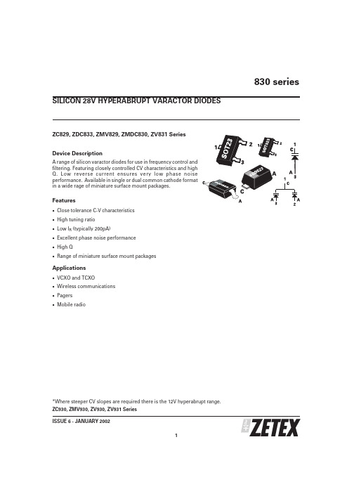
ZC829, ZDC833, ZMV829, ZMDC830, ZV831 Series Device DescriptionA range of silicon varactor diodes for use in frequency control and filtering.Featuring closely controlled CV characteristics and high Q.Low reverse current ensures very low phase noise performance.Available in single or dual common cathode format in a wide rage of miniature surface mount packages.Features·Close tolerance C-V characteristics ·High tuning ratio ·Low I R (typically 200pA)·Excellent phase noise performance ·High Q·Range of miniature surface mount packagesApplications·VCXO and TCXO·Wireless communications ·Pagers ·Mobile radio*Where steeper CV slopes are required there is the 12V hyperabrupt range.ZC930, ZMV930, ZV930, ZV931 Series 830 seriesISSUE 6 - JANUARY 20021SILICON 28V HYPERABRUPT VARACTOR DIODES830 seriesISSUE 6 - JANUARY 20022PARTCapacitance (pF)V R =2V,f=1MHzMin Q V R =3V f=50MHzCapacitance RatioC 2/C 20at f=1MHzMIN.NOM.MAX.MIN.MAX.829A 7.388.29.02250 4.3 5.8829B 7.798.28.61250 4.3 5.8830A 9.010.011.0300 4.5 6.0830B 9.510.010.5300 4.5 6.0831A 13.515.016.5300 4.5 6.0831B 14.2515.015.75300 4.5 6.0832A 19.822.024.2200 5.0 6.5832B 20.922.023.1200 5.0 6.5833A 29.733.036.3200 5.0 6.5833B 31.3533.034.65200 5.0 6.5834A 42.347.051.7200 5.0 6.5834B 44.6547.049.35200 5.0 6.5835A 61.268.074.8100 5.0 6.5835B 64.668.071.4100 5.0 6.5836A 90.0100.0110.0100 5.0 6.5836B95.0100.0105.0100 5.06.5TUNING CHARACTERISTICS at Tamb = 25°CPARAMETER SYMBOLMAX UNIT Forward currentI F 200mA Power dissipation at T amb =25ЊC SOT23P tot 330mW Power dissipation at T amb =25ЊC SOD323P tot 330mW Power dissipation at T amb =25ЊC SOD523P tot250mW Operating and storage temperature range-55to +150ЊCABSOLUTE MAXIMUM RATINGSPARAMETERCONDITIONS MIN.TYP.MAX.UNIT Reverse breakdown voltage I R =10uA 25V Reverse voltage leakageV R =20V 0.220nA Temperature coefficient of capacitanceV R =3V,f =1MHz300400ppCm/ЊCELECTRICAL CHARACTERISTICS at Tamb = 25°C830 seriesTYPICAL CHARACTERISTICSISSUE 6 - JANUARY 20023830 seriesISSUE 6 - JANUARY 20024O R D E R C O D E S A N D P A R T M A R K I N GR E E L C O D ER E E L S I Z ET A P E W I D T HQ U A N T I T Y P E R R E E LT A7i n c h (180m m )8m m3000T C13i n c h (330m m )8m m 10000T A P E A N D R E E L I N F O R M A T I O NT h e o r d e r c o d e s a r e s h o w n a s T A w h i c h i s f o r 7i n c h r e e l s .F o r 13i n c h r e e l s s u b s t i t u t e T C i n p l a c e o f T A i n t h e o r d e r c o d e .ISSUE 6 - JANUARY 20025830 seriesSOT23 PACKAGE DIMENSIONSSOD323 PACKAGE DIMENSIONSZetex plcFields New Road ChaddertonOldham, OL9 8NP United KingdomTelephone (44) 161 622 4422Fax: (44) 161 622 4420Zetex GmbHStreitfeldstraße 19D-81673 München GermanyTelefon: (49) 89 45 49 49 0Fax: (49) 89 45 49 49 49Zetex Inc700 Veterans Memorial Hwy Hauppauge, NY11788USATelephone: (631) 360 2222Fax: (631) 360 8222Zetex (Asia) Ltd3701-04Metroplaza, Tower 1Hing Fong Road Kwai Fong Hong KongTelephone: (852) 26100 611Fax: (852) 24250 494These offices are supported by agents and distributors in major countries world-wide.This publication is issued to provide outline information only which (unless agreed by the Company in writing)may not be used,applied or reproduced for any purpose or form part of any order or contract or be regarded as a representation relating to the products or services concerned.The Company reserves the right to alter without notice the specification,design,price or conditions of supply of any product or service.For the latest product information,log on to©Zetex plc 2001830 series6ISSUE 6 - JANUARY 2002DIM MILLIMETRES MIN.MAX A ᎏ0.800A10.0000.100A20.6000.800b10.1600.300c 0.0800.220D 0.7000.900E 1.500 1.700E1 1.100 1.300L 0.2000.400L10.1700.230⍜1Њ4Њ10ЊSOD523 PACKAGE DIMENSIONSSOD323 PACKAGE DIMENSIONS。
ZMV832ATA中文资料(Zetex Semiconductors)中文数据手册「EasyDatasheet - 矽搜」

SOT23 SOD523
830系列
SOT323 SOD323
*Where steeper CVslopes are required there is the 12Vhyperabrupt range. ZC930,ZMV930,ZV930,ZV931系 列
CD AE
CE AF
CF
AG
CG
ZMV8Z2M9VA8ZT2MA9VB8ZT3MA0VA8ZT3MA0VB8ZT3MA1VA8ZT3MA1VB8ZT3MA2VA8ZT3MA2VB8ZT3MA3VA8ZT3MA3VB8ZT3MA4VA8ZT3MA4VB8ZT3MA5VA8T3A5BTA
订货代码
带尺寸
7英寸13(英1寸80(毫3米30)毫米)
第 8期 - 2005年 3月 1
SEMICONDUCTORS
芯片中文手册,看全文,戳
830系列
调谐特性在环境温度 Tamb = 25°C
部分
电容( pF)
V R=2V, f=1MHz
MIN.
NOM.
MAX.
829A
7.38
8.2
9.02
829B
7.79
8.2
8.61
830A
9.0
SOT23
部 分马 克 订货代码
C2A C5A ZDC833AZTDAC834ATA
300010000
数量每卷
SOD523 订购代码和部件标记
SOD323
CS82C83H中文资料

March 199782C83H CMOS Octal Latching Inverting Bus DriverFeatures•Full 8-Bit Parallel Latching Buffer•Bipolar 8283 Compatible•Three-State Inverting Outputs•Propagation Delay . . . . . . . . . . . . . . . . . . . . . .25ns Max •Gated Inputs-Reduce Operating Power-Eliminate the Need for Pull-Up Resistors•Single 5V Power Supply•Low Power Operation-ICCSB . . . . . . . . . . . . . . . . . . . . . . . . . . . . . . . . .10mA •Operating Temperature Ranges-C82C83H . . . . . . . . . . . . . . . . . . . . . . . . .0o C to +70o C -I82C83H. . . . . . . . . . . . . . . . . . . . . . . .-40o C to +85o C -M82C83H. . . . . . . . . . . . . . . . . . . . . .-55o C to +125o C DescriptionThe Intersil 82C83H is a high performance CMOS Octal Latching Buffer manufactured using a self-aligned silicon gate CMOS process (Scaled SAJI IV). The 82C83H provides an 8-bit parallel latch/buffer in a 20 lead pin package. The active high strobe (STB) input allows transparent transfer of data and latches data on the negative transition of this signal. The active low output enable (OE) permits simple interface to microprocessor systems. The 82C83H provides inverted data at the outputs.Pinouts82C83H (PDIP, CERDIP)TOP VIEW82C83H (PLCC, CLCC)TOP VIEWOrdering InformationPART NO.PACKAGE TEMP RANGE PKG. NO CP82C83H20 Ld PDIP0o C to +70o C E20.3IP82C83H-40o C to +85o C E20.3 CS82C83H20 Ld PLCC0o C to +70o C N20.35 IS82C83H-40o C to +85o C N20.35 CD82C83H20 Ld CERDIP0o C to +70o C F20.3ID82C83H-40o C to +85o C F20.3 MD82C83H/B0o C to +70o C F20.3 8406702RA SMD#-55o C to +125o C F20.3 MR82C83H/B20 Pad CLCC-55o C to +125o C J20.A 84067022A SMD#-55o C to +125o C J20.ATRUTH TABLESTB OE DI DO X H X HI-Z H L L H H L H L ↓L X†H=Logic One L=Logic Zero X=Don‘t CareHI-Z=High Impedance↓=Negative Transition†=Latched to Value of LastData1112131415161718201910987654321DI0DI1DI2DI3DI4DI5DI7DI6OEGNDV CCDO1DO2DO3DO0DO4DO5DO6DO7STBPIN NAMESPIN DESCRIPTIONDI0 - DI7Data Input PinsDO0 - DO7Data Output PinsSTB Active High StrobeOE Active Low Output Enable1932201151617181491011121345678DI4DI5DI6DI7DI3OEGNDSTBDO7DO6DO2DO3DO4DO5DO1DI2DI1DIVCCDOFile Number2971.1CAUTION: These devices are sensitive to electrostatic discharge; follow proper IC Handling Procedures.Functional DiagramGated InputsDuring normal system operation of a latch, signals on the bus at the device inputs will become high impedance or make transitions unrelated to the operation of the latch. These unrelated input transitions switch the input circuitry and typically cause an increase in power dissipation in CMOS devices by creating a low resistance path between V CC and GND when the signal is at or near the input switch-ing threshold. Additionally, if the driving signal becomes high impedance (``float'' condition), it could create an indetermi-nate logic state at the inputs and cause a disruption in device operation.The Intersil 82C8X series of bus drivers eliminates these conditions by turning off data inputs when data is latched (STB = logic zero for the 82C82/83H) and when the device is disabled (OE = logic one for the 82C86H/87H). These gated inputs disconnect the input circuitry from the V CC and ground power supply pins by turning off the upper P-channel and lower N-channel (See Figures 1 and 2). No current flow from V CC to GND occurs during input transitions and invalid logic states from floating inputs are not transmitted. The next stage is held to a valid logic level internal to the device.D.C. input voltage levels can also cause an increase in ICC if these input levels approach the minimum V IH or maximum V IL conditions. This is due to the operation of the input cir-cuitry in its linear operating region (partially conducting state). The 82C8X series gated inputs mean that this condi-tion will occur only during the time the device is in the trans-parent mode (STB = logic one). ICC remains below the maximum ICC standby specification of 10µA during the time inputs are disabled, thereby greatly reducing the average power dissipation of the 82C8X series devices.Decoupling CapacitorsThe transient current required to charge and discharge the 300pF load capacitance specified in the 82C83H data sheet is determined byI = C L (dv/dt)Assuming that all outputs change state at the same time and that dv/dt is constant;where t R = 20ns, V CC = 5.0V, C L = 300pF on each eight out-puts.I = (8 x 300 x 10-12) x (5.0V x 0.8)/(20 x 10-9) = 480mA This current spike may cause a large negative voltage spike on V CC which could cause improper operation of the device. T o fil-ter out this noise, it is recommended that a 0.1µF ceramic disc capacitor be placed between V CC and GND at each device, with placement being as near to the device as possible.DI0DI1 DI2 DI3 DI4 DI5 DI6 DI7STBDO0DO1DO2DO3DO4DO5DO6DO7OED QCLKPPNNNPV CC V CCINTERNALDATASTBDATA INFIGURE 1.82C82/83HNNPPPNV CCV CCDATAINTERNALOEDATA INFIGURE 2.82C86H/87H GATED INPUTSI C LV CC80percent×()t R t F⁄--------------------------------------------------------=(EQ. 1)PPNNNPV CC V CCINTERNALDATASTBDATA INADDRESS ADDRESS ALEMULTI-ICCPLEXEDBUSFIGURE 3.SYSTEM EFFECTS OF GATED INPUTSAbsolute Maximum Ratings Thermal InformationSupply Voltage . . . . . . . . . . . . . . . . . . . . . . . . . . . . . . . . . . . . .+8.0V Input, Output or I/O Voltage . . . . . . . . . . . .GND 0.5V to V CC +0.5V ESD Classification . . . . . . . . . . . . . . . . . . . . . . . . . . . . . . . .Class 1 Operating ConditionsOperating Voltage Range. . . . . . . . . . . . . . . . . . . . .+4.5V to +5.5V Operating Temperature RangeC82C83H . . . . . . . . . . . . . . . . . . . . . . . . . . . . . . . . . .0o C to +70o C I82C83H. . . . . . . . . . . . . . . . . . . . . . . . . . . . . . . . . .-40o C to +85o C M82C83H. . . . . . . . . . . . . . . . . . . . . . . . . . . . . . . .-55o C to +125o C Thermal Resistance (T ypical)θJA o C/WθJC o C/W CERDIP Package . . . . . . . . . . . . . . . .7016 CLCC Package . . . . . . . . . . . . . . . . . .8020 PDIP Package. . . . . . . . . . . . . . . . . . .75N/A PLCC Package . . . . . . . . . . . . . . . . . .75N/A Storage Temperature Range. . . . . . . . . . . . . . . . . .-65o C to +150o C Max Junction T emperature Ceramic Package . . . . . . . . . . . . . .+175o C Max Junction T emperature Plastic Package. . . . . . . . . . . . . . . .+150o C Lead T emperature (Soldering 10s) (PLCC - Lead Tips Only). .+300o C Die CharacteristicsGate Count . . . . . . . . . . . . . . . . . . . . . . . . . . . . . . . . . . . .265 GatesCAUTION: Stresses above those listed in “Absolute Maximum Ratings” may cause permanent damage to the device. This is a stress only rating and operation of the device at these or any other conditions above those indicated in the operational sections of this specification is not implied.DC Electrical Specifications V CC = 5.0V± 10%; T A = 0o C to +70o C (C82C83H);T A = -40o C to +85o C (I82C83H);T A = -55o C to +125o C (M82C83H)SYMBOL PARAMETER MIN MAX UNITS TEST CONDITIONSV IH Logical One Input Voltage 2.02.2-V C82C83H, I82C83H,M82C83H, (Note 1)V IL Logical Zero Input Voltage0.8VV OH Logical One Output Voltage 3.0V CC -0.4V -V I OH = -8mA,I OH = -100mA,OE = GNDV OL Logical Zero Output Voltage0.45V I OL = 20mA,OE = GNDI I Input Leakage Current-1010µA V IN = GND or V CC,DIP Pins 1-9,11I O Output Leakage Current-1010µA V O = GND or OE≥ V CC -0.5VDIP Pins 12-19lCCSB Standby Power Supply Current-10µA V IN = V CC or GNDV CC = 5.5V Outputs OpenIC COP Operating Power Supply Current-1mA/MHz T A = +25o C, V CC = 5V, Typical (See Note 2)NOTES:1.V IH is measured by applying a pulse of magnitude = V lHMIN to one data Input at a time and checking the corresponding device output fora valid logical 1 - during valid input high time. Control pins (STB,CE) are tested separately with all device data input pins at V CC -0.4V.2.Typical ICCOP = 1 mA/MHz of STB cycle time. (Example: 5MHzµP, ALE = 1.25MHz, ICCOP = 1.25mA).Capacitance T A = +25o CSYMBOL PARAMETER TYPICAL UNITS TEST CONDITIONSC IN Input Capacitance13pF FREQ = 1MHz, all measure-ments are referenced to deviceGNDC OUT Output Capacitance20pFAC Electrical SpecificationsV CC = 5.0V ±10%; C L = 300pF (Note 1), FREQ = 1MHz T A = 0o C to +70o C (C82C83H);T A = -40o C to +85o C (l82C83H);T A = -55o C to +125o C (M82C83H)SYMBOL PARAMETERLIMITSUNITS TEST CONDITIONS MIN MAX (1) TlVOV Propagation Delay Input to Output 525 ns See Notes 2, 3(2) TSHOV Propagation Delay STB to Output 1050 ns See Notes 2, 3(3) TEHOZ Output Disable Time 522 ns See Notes 2, 3(4) TELOV Output Enable Time 1045 ns See Notes 2, 3(5) TlVSL Input to STB Set Up Time 0- ns See Notes 2, 3(6) TSLIX Input to STB Hold Time 30- ns See Notes 2, 3(7) TSHSL STB High Time 15- ns See Notes 2, 3(8) TR, TF Input Rise/Fall Times-20nsSee Notes 2, 3NOTES:1.Output load capacitance is rated 300pF for both ceramic and plastic packages.2.All AC Parameters tested as per test load circuits. Input rise and tall times are driven at 1ns/V.3.Input test signals must switch between V IL -0.4V and V lH +0.4V.Timing WaveformsAll Timing measurements are made at 1.5V unless otherwise noted.FIGURE 4.TIMING WAVEFORMSTest Load CircuitsFIGURE 5.TIVOV, TSHOV FIGURE 6.TELOV OUTPUT HIGH ENABLETR, TF (8)TIVSL (5)TSHSL (7)TSLIX (6)2.0V 0.8VTIVOV (1)TEHOZ (3)TSHOV (2)VOH -0.1V VOL +0.1VTELOV (4)3.0V 0.45VOUTPUTSOESTBINPUTS2.27V91Ω300pFTEST POINTOUTPUT(SEE NOTE)1.5V180Ω300pFTEST POINTOUTPUT(SEE NOTE)NOTE:Includes jig and stray capacitance.FIGURE 7.TELOV OUTPUT LOW ENABLEFIGURE 8.TEHOZ OUTPUT LOW/HIGH DISABLEBurn-In CircuitsFIGURE 9.MD82C83H CERDIPFIGURE 10.MR82C83H CLCCNOTES:1.V CC = 5.5V ±0.5V GND = 0V2.V IH = 4.5V ±10%3.V IL = -0.2 to 0.4V4.R1 = 47kW ±5%5.R2 = 2.0kW ±5%6.R3 = 1.0kW ±5%7.R4 = 5.0kW ±5%8.C1 = 0.01µF Minimum9.F0 = 100kHz ±10%10.F1 = F0/2, F2 = F1/2, F3 = F2/2Test Load Circuits(Continued)1.5V51Ω300pFTEST POINTOUTPUT(SEE NOTE)2.27V91Ω50pFTEST POINTOUTPUT(SEE NOTE)1112131415161718201910987654321F2F2F2F2F2F2F2F2F0R1R1R1R1R1R1R1R1R1C1V CCR1V CCR2R2AA A A A A A A A F14567891011121332120191514181716V CCC1R4R4R4R4R4R4R4F2F2F2F2F2R 3R 3R 4R 4F 0F 1V CC R 4V C C R 4R 4R 4F 2F 2F 2R4R4R422V C C2All Intersil semiconductor products are manufactured, assembled and tested under ISO9000 quality systems certification.Intersil products are sold by description only. Intersil Corporation reserves the right to make changes in circuit design and/or specifications at any time without notice. Accordingly, the reader is cautioned to verify that data sheets are current before placing orders. Information furnished by Intersil is believed to be accurate and reliable. However, no responsibility is assumed by Intersil or its subsidiaries for its use; nor for any infringements of patents or other rights of third parties which may result from its use. No license is granted by implication or otherwise under any patent or patent rights of Intersil or its subsidiaries.For information regarding Intersil Corporation and its products, see web site Die CharacteristicsDIE DIMENSIONS:138.6 x 155.5 x 19± 1 mils METALLIZATION:T ype: Silicon - Aluminum Thickness: 11k ű2k ÅGLASSIVATION:Type: SiO 2Thickness: 8k ű1k ÅWORST CASE CURRENT DENSITY:2.0 x 10⁵ A/cm 2Metallization Mask Layout82C83HDI2DI1DI2VCC DO0DO1DO2DO3DO4DO5DO6DO7STB GND OE DI7DI6DI5DI4DI3。
KS0086资料

74 SC24 73 SC23
72 SC22 71 SC21
70 SC20
69 SC19
68 SC18 67 SC17 66 SC16 65 SC15
64 SC14 63 SC13 62 SC12 61 SC11 60 SC10 59 SC9 58 SC8 57 SC7 56 SC6 55 SC5 54 SC4 53 SC3 52 SC2 51 SC1
COORDINATES
X
Y
-900
-1959
-775
-1959
-600
-1959
-475
-1959
-350
-1959
-225
-1959
-100
-1959
25
-1959
266
-1959
470
-1959
711
-1959
915
-1959
1040
-1959
1165
-1959
1290
-1959
1496
-1959
mode). • Power down function (in segment mode). • Applicable LCD duty : 1/64 ~ 1/256 • Interface
DRIVER
COM (cascade)
SEG (cascade)
KS0086
KS0086
100 TQFP-1414
80 SC30 79 SC29 78 SC28 77 SC27 76 SC26 75 SC25 74 SC24 73 SC23 72 SC22 71 SC21 70 SC20 69 SC19 68 SC18 67 SC17 66 SC16 65 SC15 64 SC14 63 SC13 62 SC12 61 SC11 60 SC10 59 SC9 58 SC8 57 SC7 56 SC6 55 SC5 54 SC4 53 SC3 52 SC2 51 SC1
RTL8316D_RTL8324D 八口16口交换机网卡数据手册
RTL8316DLAYER 2 16-PORT 10/100M SINGLE CHIPSWITCH CONTROLLERRTL8324DLAYER 2 24-PORT 10/100M SWITCHCONTROLLER WITH ONE RS8MIIDATASHEET(CONFIDENTIAL: Development Partners Only)Rev. 1.016 January 2010Track ID: JATR-2265-11No. 2, Innovation Road II, Hsinchu Science Park, Hsinchu 300, TaiwanTel.: +886-3-578-0211 Fax: +886-3-577-6047Layer 2 16-Port & 24-Port 10/100M Switch Controllers ii Track ID: JATR-2265-11 Rev. 1.0COPYRIGHT©2010 Realtek Semiconductor Corp. All rights reserved. No part of this document may be reproduced, transmitted, transcribed, stored in a retrieval system, or translated into any language in any form or by any means without the written permission of Realtek Semiconductor Corp.DISCLAIMERRealtek provides this document “as is”, without warranty of any kind. Realtek may make improvements and/or changes in this document or in the product described in this document at any time. This document could include technical inaccuracies or typographical errors.TRADEMARKSRealtek is a trademark of Realtek Semiconductor Corporation. Other names mentioned in this document are trademarks/registered trademarks of their respective owners.USING THIS DOCUMENTThis document is intended for the hardware and software engineer’s general information on the Realtek RTL8316D/RTL8324D chips.Though every effort has been made to ensure that this document is current and accurate, more information may have become available subsequent to the production of this guide.REVISION HISTORYRevision Release Date Summary 1.0 2010/01/16 First Release.Table of Contents1.GENERAL DESCRIPTION (1)2.FEATURES (2)3.BLOCK DIAGRAMS (3)3.1.RTL8316D B LOCK D IAGRAM (3)3.2.RTL8324D B LOCK D IAGRAM (4)4.SYSTEM APPLICATIONS (5)4.1.RTL8316D:16*10/100M S WITCH (5)4.2.RTL8324D:24*10/100M S WITCH (6)5.PIN ASSIGNMENTS AND DESCRIPTIONS (RTL8316D) (7)5.1.P IN A SSIGNMENTS F IGURE (RTL8316D) (7)5.2.P ACKAGE I DENTIFICATION (7)5.3.P IN A SSIGNMENTS T ABLE D EFINITIONS (RTL8316D) (8)5.4.P IN A SSIGNMENTS T ABLE (RTL8316D) (8)5.5.P IN D ESCRIPTIONS (RTL8316D) (10)5.5.1.Media Connection Pins (RTL8316D) (10)5.5.2.Serial LED/LED IC Interface Pins (RTL8316D) (11)5.5.3.SCAN LED Interface Pins (RTL8316D) (11)5.5.4.Miscellaneous Interface Pins (RTL8316D) (11)5.5.5.GPIO Interface Pins (RTL8316D) (12)5.5.6.Configuration Strapping Pins (RTL8316D) (12)5.5.7.Power and GND Pins (RTL8316D) (13)6.PIN ASSIGNMENTS AND DESCRIPTIONS (RTL8324D) (14)6.1.P IN A SSIGNMENTS F IGURE (RTL8324D) (14)6.2.P ACKAGE I DENTIFICATION (14)6.3.P IN A SSIGNMENTS T ABLE D EFINITIONS (RTL8324D) (15)6.4.P IN A SSIGNMENTS T ABLE (RTL8324D) (15)6.5.P IN D ESCRIPTIONS (RTL8324D) (17)6.5.1.Media Connection Pins (RTL8324D) (17)6.5.2.Serial LED Interface Pins (RTL8324D) (18)6.5.3.Miscellaneous Interface Pins (RTL8324D) (18)6.5.4.GPIO Interface Pins (RTL8324D) (18)6.5.5.Configuration Strapping Pins (RTL8324D) (19)6.5.6.RS8MII Interface Pins (RTL8324D) (19)6.5.7.Power and GND Pins (RTL8324D) (20)7.PHYSICAL LAYER FUNCTIONAL OVERVIEW (21)7.1.MDI I NTERFACE (21)7.2.100B ASE-TX T RANSMIT F UNCTION (21)7.3.100B ASE-TX R ECEIVE F UNCTION (21)7.4.10B ASE-T T RANSMIT F UNCTION (21)7.5.10B ASE-T R ECEIVE F UNCTION (21)7.6.A UTO-N EGOTIATION FOR UTP (22)7.7.C ROSSOVER D ETECTION AND A UTO C ORRECTION (22)7.8.P OLARITY C ORRECTION (22)8.SWITCH FUNCTION DESCRIPTION (23)8.1.H ARDWARE R ESET AND S OFTWARE R ESET (23)Layer 2 16-Port & 24-Port 10/100M Switch Controllers iii Track ID: JATR-2265-11 Rev. 1.08.1.2.Software Reset (23)8.2.L AYER 2L EARNING AND F ORWARDING (23)8.2.1.Forwarding (23)8.2.2.Learning (24)8.2.3.Address Table Aging (24)8.3.L AYER 2M ULTICAST AND IP M ULTICAST (24)8.4.R ESERVED M ULTICAST A DDRESS H ANDLING (24)8.5.IEEE802.3X F LOW C ONTROL (25)8.6.H ALF D UPLEX B ACKPRESSURE (25)8.6.1.Collision-Based Backpressure (Jam Mode) (25)8.6.2.Carrier-Based Backpressure (Defer Mode) (26)8.7.P RE-IEEE802.3AZ E NERGY E FFICIENT E THERNET (EEE) (26)8.8.G REEN E THERNET (27)8.8.1.Link Down Power Saving (27)8.8.2.Link On Various Cable Length Power Saving (27)8.9.IEEE802.1P AND IEEE802.1Q(VLAN) (27)8.10.L OOP D ETECTION (27)8.11.L AYER 2T RAFFIC S UPPRESSION (S TORM C ONTROL) (27)8.12.IEEE802.3AD L INK A GGREGATION P ROTOCOL (28)8.13.B ANDWIDTH C ONTROL (28)8.13.1.Input Bandwidth Control (28)8.13.2.Output Bandwidth Control (28)8.14.Q UALITY OF S ERVICE (Q O S) (28)8.14.1.Priority Arbitration (28)8.14.2.Port-Based Priority Assignment (28)8.14.3.IEEE 802.1Q-Based Priority Assignment (29)8.14.4.DSCP-Based Priority Assignment (29)8.14.5.Internal Priority to Queue ID Table (29)8.15.P ACKET S CHEDULING (WRR AND WFQ) (29)8.16.E GRESS P ACKET R EMARKING (29)8.17.I NGRESS AND E GRESS P ORT M IRROR (30)8.18.M ANAGEMENT I NFORMATION B ASE (MIB) (30)8.19.R EALTEK C ABLE T ESTER (30)8.20.EEPROM C ONFIGURATION (31)8.21.CPU F UNCTION D ESCRIPTION (31)9.INTERFACE DESCRIPTIONS (32)9.1.RS8MII I NTERCONNECTION (32)9.2.I2C-L IKE LED (32)9.3.S ERIAL LED C ONNECTION (33)9.4.S CAN LED FOR RTL8316D (34)9.5.I2C M ASTER FOR EEPROM (35)9.6.I2C S LAVE FOR E XTERNAL CPU (35)10.ELECTRICAL AC/DC CHARACTERISTICS (36)10.1.A BSOLUTE M AXIMUM R ATINGS (36)10.2.O PERATING R ANGE (36)10.3.DC C HARACTERISTICS (36)10.4.AC C HARACTERISTICS (37)10.4.1.RS8MII Transmitter Signal Electrical Characteristics (37)10.4.2.RS8MII Receiver Signal Electrical Characteristics (37)10.4.3.Serial LED Signal Timing (37)10.4.4.Scan LED Mode Signal Timing (RTL8316D) (38)10.4.5.I2C Master for EEPROM Timing (38)Layer 2 16-Port & 24-Port 10/100M Switch Controllers iv Track ID: JATR-2265-11 Rev. 1.010.4.7.EEPROM Auto-Load Timing (39)10.4.8.I2C Master Mode Timing Characteristics (39)10.4.9.I2C Slave Mode Timing (40)10.4.10.I2C Slave Mode Timing Characteristics (40)11.PACKAGE INFORMATION (41)11.1.LQFP128E-PAD (41)12.ORDERING INFORMATION (42)List of TablesT ABLE 1.P IN A SSIGNMENTS T ABLE (RTL8316D) (8)T ABLE 2.M EDIA C ONNECTION P INS (RTL8316D) (10)T ABLE 3.S ERIAL LED/LED IC I NTERFACE P INS (RTL8316D) (11)T ABLE 4.SCAN LED I NTERFACE P INS (RTL8316D) (11)T ABLE 5.M ISCELLANEOUS I NTERFACE P INS (RTL8316D) (11)T ABLE 6.GPIO I NTERFACE P INS (RTL8316D) (12)T ABLE 7.C ONFIGURATION S TRAPPING P INS (RTL8316D) (12)T ABLE 8.P OWER AND GND P INS (RTL8316D) (13)T ABLE 9.RTL8324D P IN A SSIGNMENTS T ABLE (RTL8324D) (15)T ABLE 10.M EDIA C ONNECTION P INS (RTL8324D) (17)T ABLE 11.LED I NTERFACE P INS (RTL8324D) (18)T ABLE 12.M ISCELLANEOUS I NTERFACE P INS (RTL8324D) (18)T ABLE 13.GPIO I NTERFACE P INS (RTL8324D) (18)T ABLE 14.C ONFIGURATION S TRAPPING P INS (RTL8324D) (19)T ABLE 15.RS8MII I NTERFACE P INS (RTL8324D) (19)T ABLE 16.P OWER AND GND P INS (RTL8324D) (20)T ABLE 17.R ESERVED M ULTICAST A DDRESS D EFAULT A CTIONS (24)T ABLE 18.A BSOLUTE M AXIMUM R ATINGS (36)T ABLE 19.R ECOMMENDED O PERATING R ANGE (36)T ABLE 20.DC C HARACTERISTICS (36)T ABLE 21.RS8MII T RANSMITTER S IGNAL E LECTRICAL C HARACTERISTICS (37)T ABLE 22.RS8MII R ECEIVER S IGNAL E LECTRICAL C HARACTERISTICS (37)T ABLE 23.I2C M ASTER M ODE T IMING C HARACTERISTICS (39)T ABLE 24.I2C S LAVE M ODE T IMING C HARACTERISTICS (40)T ABLE 25.O RDERING I NFORMATION (42)Layer 2 16-Port & 24-Port 10/100M Switch Controllers v Track ID: JATR-2265-11 Rev. 1.0List of FiguresF IGURE 1.RTL8316D B LOCK D IAGRAM (3)F IGURE 2.RTL8324D B LOCK D IAGRAM (4)F IGURE 3.RTL8316D:16*10/100M S WITCH (5)F IGURE 4.RTL8324D:24*10/100M S WITCH (6)F IGURE 5.P IN A SSIGNMENTS (RTL8316D) (7)F IGURE 6.P IN A SSIGNMENTS (RTL8324D) (14)F IGURE 7.C ONCEPTUAL E XAMPLE OF P OLARITY C ORRECTION (22)F IGURE 8.T X P AUSE F RAME F ORMAT (25)F IGURE 9.F LOW C ONTROL S TATE M ACHINE (25)F IGURE 10.C OLLISION-B ASED B ACKPRESSURE S IGNAL T IMING (26)F IGURE 11.RS8MII I NTERCONNECTION (32)F IGURE 12.S ERIAL LED C ONNECTION (33)F IGURE 13.S CAN LED M ODE C ONNECTION (34)F IGURE 14.L ARGE S IZE (32K B~512K B)EEPROM R EAD/W RITE T IMING (35)F IGURE 15.S MALL S IZE (4K B~8K B)EEPROM R EAD/W RITE T IMING (35)F IGURE 16.I2C A CCESS D ATA S EQUENCE (35)F IGURE 17.S ERIAL LED S IGNAL T IMING (37)F IGURE 18.S CAN LED M ODE S IGNAL T IMING (RTL8316D) (38)F IGURE 19.I2C M ASTER M ODE T IMING (38)F IGURE 20.SCK/SDA P OWER ON T IMING (39)F IGURE 21.EEPROM A UTO-L OAD T IMING (39)F IGURE 22.I2C S LAVE M ODE T IMING (40)Layer 2 16-Port & 24-Port 10/100M Switch Controllers vi Track ID: JATR-2265-11 Rev. 1.01.General DescriptionThe RTL8316D/RTL8324D are Layer 2 16/24-port 10/100M switch controllers that integrate 16/24 MACs and 16 physical layer transceivers for 100Base-TX and 10Base-T operation.The RTL8324D (only) supports one RS8MII (Reduced Serial eight Media Independent Interface), which can be connected to an Octal PHY RTL8208D to provide a convenient solution for a 24-port Fast Ethernet switch.The RTL8316D/RTL8324D features an embedded 8051 MPU to execute programs via an external EEPROM.The RTL8316D/RTL8324D provides a 2Mbit packet buffer for wire-speed forwarding capability. There is an 8K-entry L2 table with a 4-way hash algorithm for MAC address learning and searching, and a 256-entry forwarding table to support L2 multicast functions. The RTL8316D/RTL8324D supports IVL (Independent VLAN Learning), SVL (Shared VLAN Learning), and IVL/SVL (Both Independent and Shared VLAN Learning) for flexible network topology architecture. The RTL8316D/RTL8324D has a 512-entry VLAN table and 16-entry VLAN CAM table for VLAN operation.Per-port ingress/egress bandwidth control and per-port/per-queue egress bandwidth control are supported, with four physical queues in each port. The RTL8316D/RTL8324D provides three types of packet scheduling, including SP (Strict Priority), WRR (Weighted Round Robin) and WFQ (Weighted Fair Queuing).A loop-detection function provides notification of network loops. The RTL8316D/RTL8324D also supports port mirror configuration to mirror ingress and egress traffic, and link aggregation to increase link bandwidth and redundancy.Layer 2 16-Port & 24-Port 10/100M Switch Controllers 1Track ID: JATR-2265-11 Rev. 1.0Layer 2 16-Port & 24-Port 10/100M Switch Controllers 2 Track ID: JATR-2265-11 Rev. 1.02. FeaturesHardware InterfaceRTL8316D provides 16-port 10/100Mhigh performance Ethernet switch controllers, and 16 FE PHYs for 100Base-TX and 10Base-TRTL8324D provides 24-port 10/100Mhigh performance Ethernet switch controllers, and 16 FE PHYs for 100Base-TX and 10Base-TRTL8324D (only) supports RS8MIIinterface to connect with octal FE PHYRTL8316D (only) supports SCAN LED RTL8316D/RTL8324D Support serialLED interfaceMAC Function2Mbit SRAM Packet Buffer Supports 2KB jumbo frame 8K-entry L2 MAC table with 4-wayhashing algorithmIndependent 256-entry Forwarding tablefor multicast AddressesSupports source MAC blocking andDestination MAC blockingSupports Reserved Multicast AddressesprocessingSupports MAC Address learningconstraints on each portVLAN FunctionSupports IVL, SVL, and IVL/SVL Supports IEEE 802.1Q VLAN512-entry VLAN Table Port-based VLAN L2 Miscellaneous FunctionsSupports RLPP (Realtek LoopPrevention Protocol)Supports cable diagnostics technology Supports broadcast, multicast, unknown-multicast, and unknown-unicast packet suppression controlSupports IEEE 802.3az (EnergyEfficient Ethernet, EEE) and Realtek Green EthernetSupports TX and RX Port Mirroring Supports Link Aggregation(IEEE 802.3ad) for 4 groups of linkaggregators with up to 8 ports per-groupPort isolation function enhances portsecurityQoS Functions4 priority queues per portSupports SP, WRR, WFQ scheduling Ingress and egress rate limiting per portMIB FunctionsRFC2819 -- RMON MIB group 1, 2, 3, 9 RFC3635/RFC2863/RFC1213/RFC4188/RFC4363Others0.11µm CMOS process 3.3V/1.2V dual power input LQFP128 E-PAD package3.Block Diagrams3.1.RTL8316D Block DiagramFigure 1. RTL8316D Block DiagramLayer 2 16-Port & 24-Port 10/100M Switch Controllers 3Track ID: JATR-2265-11 Rev. 1.03.2.RTL8324D Block DiagramFigure 2. RTL8324D Block DiagramLayer 2 16-Port & 24-Port 10/100M Switch Controllers 4Track ID: JATR-2265-11 Rev. 1.04.System Applications4.1.RTL8316D: 16*10/100M SwitchFigure 3. RTL8316D: 16*10/100M SwitchLayer 2 16-Port & 24-Port 10/100M Switch Controllers 5Track ID: JATR-2265-11 Rev. 1.0Layer 2 16-Port & 24-Port 10/100M Switch Controllers 6Track ID: JATR-2265-11 Rev. 1.04.2.RTL8324D: 24*10/100M Switch8*M D ID IFigure 4. RTL8324D: 24*10/100M SwitchLayer 2 16-Port & 24-Port 10/100M Switch Controllers 7Track ID: JATR-2265-11 Rev. 1.05. Pin Assignments and Descriptions (RTL8316D)For RTL8324D Pin Assignments and Descriptions, see section 6 Pin Assignments and Descriptions, page 14.5.1. Pin Assignments Figure (RTL8316D)D V D D 12LE D _S T A 2L E D _S T A 3L E D _S T A 4L E D _S T A 5L E D _S C A N 0/D I S _F C L E D _S C A N 1/E N _I S LL E D _S C A N 2/L E D _D E F L E D _S C A N 3/L E D _M O D E _0L E D _S C A N 4/E E P R O M T Y P E L E D _S C A N 5/C P U _M O D E D V D D 33T X O P 5R X I N 5T X O N 5R X I P 5A V D D 12T X O N 6T X O P 6R X I N 6R X I P 6T X O P 9R X I N 9T X O N 9R X I P 9A V D D 33T X O P 7T X O N 7R X I P 7R X I N 7T X O P 8T X O N 8R X I N 8R X I P 8A V D D 33D V D D 12A V D D 12X I A V D D 33_X T A L X O V D D 12_P L L A V D D 33T X O N 4T X O P 4R X I N 4R X I P 4AVDD33IBREF TXOP0RXIN0TXON0RXIP0AVDD33TXON1TXOP1RXIN1RXIP1TXOP2RXIN2TXON2RXIP2AVDD33AVDD12TXON3TXOP3RXIN3RXIP3L E D _S T A 0A V D D 12AVDD12AVDD12DVDD12T X O P 10T X O N 10R X I P 10R X I N 10TXOP12TXON12RXIN12RXIP12AVDD33TXOP11TXON11RXIN11RXIP11A V D D 12TXOP13TXON13RXIP13RXIN13TXOP15TXOP14TXON15RXIP15TXON14RXIN14RXIP14RXIN15AVDD33AVDD12D V D D 12A V D D 33AVDD12D V D D 12D V D D 12L E D _S T A 1DVDD12R E S E T #I 2C _S D A I 2C _S C K D V D D 33D V D D 12F D R #/G P I O 6D V D D 33L E D _C KL E D _D A G N D _P L L G N D _R E X T G P O 4/P H Y _P W R D O W N G P O 5/E N _S T O R M F I L T E R DVDD12D V D D 12AVDD12AVDD33G P I O 1G P I O 0G P I O 2G P O 3/L E D _M o d e _1Figure 5. Pin Assignments (RTL8316D)5.2. Package IdentificationGreen package is indicated by a ‘G’ in the location marked ‘T’.Layer 2 16-Port & 24-Port 10/100M Switch Controllers 8Track ID: JATR-2265-11 Rev. 1.05.3. Pin Assignments Table Definitions (RTL8316D)Upon Reset: Defined as a short time after the end of a hardware reset. After Reset: Defined as the time after the specified ‘Upon Reset’ time.I: Input Pin AI:Analog Input Pin O: Output PinAO:Analog Output PinI/O: Bi-Direction Input/Output Pin AI/O:Analog Bi-Direction Input/Output Pin P: Digital Power Pin AP:Analog Power Pin G: Digital Ground PinAG:Analog Ground PinI PU : Input Pin With Pull-Up Resistor;(Typical Value is about 75K Ω) O PU :Output Pin With Pull-Up Resistor;(Typical Value is about 75K Ω) I PD : Input Pin With Pull-Down Resistor;(Typical Value is about 75K Ω)O PD :Output Pin With Pull-Down Resistor;(Typical Value is about 75K Ω)5.4. Pin Assignments Table (RTL8316D)Table 1. Pin Assignments Table (RTL8316D)Name Pin No. Type DVDD12 1 P A VDD12 2 AP RXIP4 3 AI/O RXIN4 4 AI/O TXOP4 5 AI/O TXON4 6 AI/O A VDD33 7 AP TXON5 8 AI/O TXOP5 9 AI/O RXIN5 10 AI/O RXIP5 11 AI/O A VDD12 12 AP RXIP6 13 AI/O RXIN6 14 AI/O TXOP6 15 AI/O TXON6 16 AI/O A VDD33 17 AP TXON7 18 AI/O TXOP7 19 AI/O Name Pin No. Type RXIN7 20 AI/O RXIP7 21 AI/O A VDD12 22 AP RXIP8 23 AI/O RXIN8 24 AI/O TXOP8 25 AI/O TXON8 26 AI/O A VDD33 27 AP TXON9 28 AI/O TXOP9 29 AI/O RXIN9 30 AI/O RXIP9 31 AI/O A VDD12 32 AP RXIP10 33 AI/O RXIN10 34 AI/O TXOP10 35 AI/O TXON10 36 AI/O A VDD33 37 AP DVDD12 38 PLayer 2 16-Port & 24-Port 10/100M Switch Controllers 9Track ID: JATR-2265-11 Rev. 1.0A VDD33 39 AP TXON11 40 AI/O TXOP11 41 AI/O RXIN11 42 AI/O RXIP11 43 AI/O A VDD12 44 AP RXIP12 45 AI/O RXIN12 46 AI/O TXOP12 47 AI/O TXON12 48 AI/O A VDD33 49 AP TXON13 50 AI/O TXOP13 51 AI/O RXIN13 52 AI/O RXIP13 53 AI/O A VDD12 54 AP RXIP14 55 AI/O RXIN14 56 AI/O TXOP14 57 AI/O TXON14 58 AI/O A VDD33 59 AP TXON15 60 AI/O TXOP15 61 AI/O RXIN15 62 AI/O RXIP15 63 AI/O A VDD12 64 AP DVDD12 65 P DVDD12 66 P LED_SCAN5/CPU_MODE 67 I/O PD LED_SCAN4/EEPROMTYPE 68 I/O PD LED_SCAN3/LED_MODE_1 69 I/O PD LED_SCAN2/LED_DEF 70 I/O PD DVDD33 71 P LED_SCAN1/EN_ISL 72 I/O PD LED_SCAN0/DIS_FC 73 I/O PD LED_STA5 74 O LED_STA4 75 O DVDD12 76 P LED_STA3 77 O LED_STA2 78 O LED_STA1 79 O LED_STA0 80 O DVDD33 81 P GND_REXT 82 AG A VDD33_XTAL 83 AP XO 84 AO XI 85 AI GND_PLL 86 AG VDD12_PLL 87 AP DVDD12 88 P GPIO0 89 O PD GPIO1 90 O PD GPIO2 91 O PD GPO3/LED_MODE_1 92 O PD GPO4/PHY_PWRDOWN 93 O PD GPO5/EN_STORMFILTER 94 O PD DVDD33 95 P I2C_SDA 96 I/O PU I2C_SCK 97 O PU LED_DA 98 I/O PU LED_CK 99 O PU FDR#/GPIO6 100 I/O PU RESET# 101 AI PU DVDD12 102 P DVDD12 103 P A VDD33 104 AP IBREF 105 AO A VDD12 106 AP RXIP0 107 AI/O RXIN0 108 AI/O TXOP0 109 AI/O TXON0 110 AI/O A VDD33 111 AP TXON1 112 AI/O TXOP1 113 AI/O RXIN1 114 AI/O RXIP1 115 AI/O A VDD12 116 AP RXIP2 117 AI/O RXIN2 118 AI/O TXOP2 119 AI/O TXON2 120 AI/O A VDD33 121 AP TXON3 122 AI/O TXOP3 123 AI/O RXIN3 124 AI/O RXIP3 125 AI/O A VDD12 126 APLayer 2 16-Port & 24-Port 10/100M Switch Controllers 10 Track ID: JATR-2265-11 Rev. 1.0DVDD12 127 P DVDD12 128 PDGND EPAD G5.5. Pin Descriptions (RTL8316D)5.5.1. Media Connection Pins (RTL8316D)Table 2. Media Connection Pins (RTL8316D) Pin NamePin No. Type Drive (mA) DescriptionRXIP15/RXIN15 RXIP14/RXIN14 RXIP13/RXIN13 RXIP12/RXIN12 RXIP11/RXIN11 RXIP10/RXIN10 RXIP9/RXIN9 RXIP8/RXIN8 RXIP7/RXIN7 RXIP6/RXIN6 RXIP5/RXIN5 RXIP4/RXIN4 RXIP3/RXIN3 RXIP2/RXIN2 RXIP1/RXIN1 RXIP0/RXIN0 63, 6255,5653, 52 45, 46 43, 42 33, 34 31, 30 23, 24 21, 20 15, 16 11, 10 3, 4 125, 124 117, 118 115, 114 107, 108AI - Differential Receive Data Input: Port0-15 support 100Base-TX, 10Base-T TXOP15/TXON15 TXOP14/TXON14 TXOP13/TXON13 TXOP12/TXON12 TXOP11/TXON11 TXOP10/TXON10 TXOP9/TXON9 TXOP8/TXON8 TXOP7/TXON7 TXOP6/TXON6 TXOP5/TXON5 TXOP4/TXON4 TXOP3/TXON3 TXOP2/TXON2 TXOP1/TXON1 TXOP0/TXON061, 6057, 5851, 50 47, 48 41, 40 35, 36 29, 28 25, 26 19, 18 15, 16 9, 8 5, 6 123, 122 119, 120 113, 112 109, 110AO - Differential Transmit Data Output: Port0-15 support 100Base-TX, 10Base-TLayer 2 16-Port & 24-Port 10/100M Switch Controllers 11 Track ID: JATR-2265-11 Rev. 1.05.5.2. Serial LED/LED IC Interface Pins (RTL8316D)Table 3. Serial LED/LED IC Interface Pins (RTL8316D) Pin Name Pin No. Type Drive (mA) Description LED_CK99 O 4 (1) In Serial LED mode:Reference output clock for serial LED interface and Data is latched on the rising of LEDCK. (2) In I 2C-like LED mode:Reference output clock for I 2C-like interface.LED_DA98 O 4 Serial LED Data Output.In Serial LED mode:Serial bit stream of link status information. In I 2C-like LED mode:The data written to LED IC.5.5.3. SCAN LED Interface Pins (RTL8316D)Table 4. SCAN LED Interface Pins (RTL8316D) Pin Name Pin No. Type Drive (mA) DescriptionLED_STA[5:0] 74, 75, 77, 78,79, 80O PD 8 Scan LED Mode status Pins. LED_SCAN[5:0]67, 68, 69, 70,72, 73O PD 8 Scan LED mode scan pins.5.5.4. Miscellaneous Interface Pins (RTL8316D)Table 5. Miscellaneous Interface Pins (RTL8316D)Pin Name Pin No. Type Drive (mA) Description I2C_SCK 97 I/O PU 4 I 2C Interface Clock.For normal mode (100KHz), a cycle time is 10µs. For fast mode (400KHz), it is 2.5µs.I2C_SDA 96 I/O PU 4 I 2C Interface Data Input/Output. FDR#100I-Factory default recovery input pin.It takes effect when it is asserted low at least 3 seconds.XI 85 AI - 25MHz Crystal Clock Input and Feedback Pin. XO84 AO - 25MHz Crystal Clock Output Pin. RESET# 101 AI - System Pin Reset Input.IBREF 105 AO -Reference Resistor for PHY bandgap.A 2.49K Ω (1%) resistor should be connected between IBREF and GND.Layer 2 16-Port & 24-Port 10/100M Switch Controllers 12 Track ID: JATR-2265-11 Rev. 1.05.5.5. GPIO Interface Pins (RTL8316D)Table 6. GPIO Interface Pins (RTL8316D)Pin Name Pin No. Type Drive (mA) Description GPIO[2:0] 91, 90, 89 I/O PD 4 General Purpose Input/Output pins. GPO[5:3] 94, 93, 92 O PD 4 General Purpose Output pins. GPIO6 100 I/O PU 4 General Purpose Input/Output pins.5.5.6. Configuration Strapping Pins (RTL8316D)Table 7. Configuration Strapping Pins (RTL8316D) Pin Name Pin No. Type Default Description CPU_MODE 67 I PD - Enable or Disable Internal 8051.0: Enable (default) 1: DisableEEPROMTYPE 68 I PD - Select EEPROM Auto-Load Address Byte Size.0: 2-Byte (default) 1: 1-ByteLED_MODE[1:0] 92, 69 I PD - LED Mode Select.00: Serial LED mode (default) 01: I 2C-like LED mode 10: SCAN LED mode 11: ReservedLED_DEF 70 I PD - LED Status Default Mode Select.0: Select mode0 (default) 1: Select mode1EN_ISL 72 I PD - Enable Port Isolation.0: Disable port isolation (default) 1: Enable port isolationDIS_FC 73 I PD - Enable All Port Flow Control.0: Enable (default) 1: DisablePHY_PWRDOWN 93 I PD - Enable PHY Power Down When Power On.0: Normal (default)1: Enable PHY power down when power onEN_STORMFILTER 94 I PD - Enable Broadcast Storm Filter.0: Disable traffic storm filter (default) 1: Enable traffic storm filterLayer 2 16-Port & 24-Port 10/100M Switch Controllers 13 Track ID: JATR-2265-11 Rev. 1.05.5.7. Power and GND Pins (RTL8316D)Table 8. Power and GND Pins (RTL8316D)Pin Name Pin No. Type Description A VDD33 7, 17, 27, 37, 39, 49, 59,104, 111, 121AP Analog Power 3.3V . A VDD12 2, 12, 22, 32, 44, 54, 64,106, 116, 126AP Analog Power 1.2V . DVDD33 71, 81, 95 P Digital Power 3.3V for IO Pad. DVDD12 1, 38, 65, 66, 76, 88, 102,103, 127, 128P Digital Power 1.2V for Core V oltage. VDD12_PLL 87 AP Power for PLL. GND_PLL 86 AG Ground for PLL. A VDD33_XTAL 83 AP Analog Power for Crystal.Layer 2 16-Port & 24-Port 10/100M Switch Controllers 14 Track ID: JATR-2265-11 Rev. 1.06. Pin Assignments and Descriptions (RTL8324D)For RTL8324D Pin Assignments and Descriptions, see section 5 Pin Assignments and Descriptions (RTL8316D), page 7.6.1. Pin Assignments Figure (RTL8324D)A V S S 25M _C L K O S R X N S A V D D 12S R X P S A V D D 12R E X T X I A V D D 33_X T A L X O S T X P S T X N A V S S S A V D D 12V D D 12_P L L D V D D 12D V D D 12D V D D 12RE S E T #I 2C _S D A I 2C _S C K L E D _D A L E D _C K D V D D 33D V D D 12M D I O M D CF D R #/G P I O 6G N D _P L L G N D _R E X T G P O 5/C P U _M O D E D V D D 33G P O 4/E E P R O M T Y P E G P O 3/L E D _M O D E G P O 2/L E D _D E F G P I O 1/E N _I S L G P I O 0/D I S _F C D V D D 12T X O P 5R X I N 5T X O N 5R X I P 5A V D D 12T X O N 6T X O P 6R X I N 6R X I P 6T X O P 9R X I N 9T X O N 9R X I P 9A V D D 33T X O P 7T X O N 7R X I P 7R X I N 7T X O P 8T X O N 8R X I N 8R X I P 8A V D D 33D V D D 12A V D D 12A V D D 33T X O N 4T X O P 4R X I N 4R X I P 4AVDD33IBREF TXOP0RXIN0TXON0RXIP0AVDD33TXON1TXOP1RXIN1RXIP1TXOP2RXIN2TXON2RXIP2AVDD33AVDD12TXON3TXOP3RXIN3RXIP3A V D D 12AVDD12AVDD12DVDD12T X O P 10T X O N 10R X I P 10R X I N 10TXOP12TXON12RXIN12RXIP12AVDD33TXOP11TXON11RXIN11RXIP11A V D D 12TXOP13TXON13RXIP13RXIN13TXOP15TXOP14TXON15RXIP15TXON14RXIN14RXIP14RXIN15AVDD33AVDD12D V D D 12A V D D 33AVDD12DVDD12DVDD12AVDD12AVDD33Figure 6. Pin Assignments (RTL8324D)6.2. Package IdentificationGreen package is indicated by a ‘G’ in the location marked ‘T’.Layer 2 16-Port & 24-Port 10/100M Switch Controllers 15Track ID: JATR-2265-11 Rev. 1.06.3. Pin Assignments Table Definitions (RTL8324D)Upon Reset: Defined as a short time after the end of a hardware reset. After Reset: Defined as the time after the specified ‘Upon Reset’ time.I: Input Pin AI:Analog Input Pin O: Output PinAO:Analog Output PinI/O: Bi-Direction Input/Output Pin AI/O:Analog Bi-Direction Input/Output Pin P: Digital Power Pin AP:Analog Power Pin G: Digital Ground PinAG:Analog Ground PinI PU : Input Pin With Pull-Up Resistor;(Typical Value approximately 75K Ω) O PU :Output Pin With Pull-Up Resistor;(Typical Value approximately 75K Ω) I PD : Input Pin With Pull-Down Resistor;(Typical Value approximately 75K Ω)O PD :Output Pin With Pull-Down Resistor;(Typical Value approximately 75K Ω)6.4. Pin Assignments Table (RTL8324D)Table 9. RTL8324D Pin Assignments Table (RTL8324D)Name Pin No. Type DVDD12 1 P A VDD12 2 AP RXIP4 3 AI/O RXIN4 4 AI/O TXOP4 5 AI/O TXON4 6 AI/O A VDD33 7 AP TXON5 8 AI/O TXOP5 9 AI/O RXIN5 10 AI/O RXIP5 11 AI/O A VDD12 12 AP RXIP6 13 AI/O RXIN6 14 AI/O TXOP6 15 AI/O TXON6 16 AI/O A VDD33 17 AP TXON7 18 AI/O TXOP7 19 AI/O Name Pin No. Type RXIN7 20 AI/O RXIP7 21 AI/O A VDD12 22 AP RXIP8 23 AI/O RXIN8 24 AI/O TXOP8 25 AI/O TXON8 26 AI/O A VDD33 27 AP TXON9 28 AI/O TXOP9 29 AI/O RXIN9 30 AI/O RXIP9 31 AI/O A VDD12 32 AP RXIP10 33 AI/O RXIN10 34 AI/O TXOP10 35 AI/O TXON10 36 AI/O A VDD33 37 AP DVDD12 38 PLayer 2 16-Port & 24-Port 10/100M Switch Controllers 16Track ID: JATR-2265-11 Rev. 1.0A VDD33 39 AP TXON11 40 AI/O TXOP11 41 AI/O RXIN11 42 AI/O RXIP11 43 AI/O A VDD12 44 AP RXIP12 45 AI/O RXIN12 46 AI/O TXOP12 47 AI/O TXON12 48 AI/O A VDD33 49 AP TXON13 50 AI/O TXOP13 51 AI/O RXIN13 52 AI/O RXIP13 53 AI/O A VDD12 54 AP RXIP14 55 AI/O RXIN14 56 AI/O TXOP14 57 AI/O TXON14 58 AI/O A VDD33 59 AP TXON15 60 AI/O TXOP15 61 AI/O RXIN15 62 AI/O RXIP15 63 AI/O A VDD12 64 AP DVDD12 65 P DVDD12 66 P GPO5/CPU_MODE 67 O PD GPO4/EEPROMTYPE 68 O PD GPO3/LED_MODE 69 O PD GPO2/LED_DEF 70 O PD DVDD33 71 P GPIO1/EN_ISL 72 I/O PD GPIO0/DIS_FC 73 I/O PD DVDD12 74 P SA VDD12 75 AP SRXN 76 AI SRXP 77 AI A VSS 78 AG 25M_CLKO 79 O SA VDD12 80 AP STXP 81 AO STXN 82 AO A VSS 83 AG SA VDD12 84 AP GND_REXT 85 AG REXT 86 AO A VDD33_XTAL 87 AP XO 88 AO XI 89 AI GND_PLL 90 AG VDD12_PLL 91 AP DVDD12 92 P MDC 93 O PU MDIO 94 I/O PU DVDD33 95 P I2C_SDA 96 I/O PU I2C_SCK 97 O PU LED_DA 98 I/O PU LED_CK 99 O PU FDR#/GPIO6 100 I/O PU RESET# 101 AI PU DVDD12 102 P DVDD12 103 P A VDD33 104 AP IBREF 105 AO A VDD12 106 AP RXIP0 107 AI/O RXIN0 108 AI/O TXOP0 109 AI/O TXON0 110 AI/O A VDD33 111 AP TXON1 112 AI/O TXOP1 113 AI/O RXIN1 114 AI/O RXIP1 115 AI/O A VDD12 116 AP RXIP2 117 AI/O RXIN2 118 AI/O TXOP2 119 AI/O TXON2 120 AI/O A VDD33 121 AP TXON3 122 AI/O TXOP3 123 AI/O RXIN3 124 AI/O RXIP3 125 AI/O A VDD12 126 APLayer 2 16-Port & 24-Port 10/100M Switch Controllers 17 Track ID: JATR-2265-11 Rev. 1.0DVDD12 127 P DVDD12 128 PDGND EPAD G6.5. Pin Descriptions (RTL8324D)6.5.1. Media Connection Pins (RTL8324D)Table 10. Media Connection Pins (RTL8324D) Pin NamePin No. Type Drive (mA) DescriptionRXIP15/RXIN15 RXIP14/RXIN14 RXIP13/RXIN13 RXIP12/RXIN12 RXIP11/RXIN11 RXIP10/RXIN10 RXIP9/RXIN9 RXIP8/RXIN8 RXIP7/RXIN7 RXIP6/RXIN6 RXIP5/RXIN5 RXIP4/RXIN4 RXIP3/RXIN3 RXIP2/RXIN2 RXIP1/RXIN1 RXIP0/RXIN0 63, 6255, 5653, 52 45, 46 43, 42 33, 34 31, 30 23, 24 21, 20 15, 16 11, 10 3, 4 125, 124 117, 118 115, 114 107, 108AI - Differential Receive Data Input: Port0-15 supports 100Base-TX, 10Base-T TXOP15/TXON15 TXOP14/TXON14 TXOP13/TXON13 TXOP12/TXON12 TXOP11/TXON11 TXOP10/TXON10 TXOP9/TXON9 TXOP8/TXON8 TXOP7/TXON7 TXOP6/TXON6 TXOP5/TXON5 TXOP4/TXON4 TXOP3/TXON3 TXOP2/TXON2 TXOP1/TXON1 TXOP0/TXON061, 6057, 5851, 50 47, 48 41, 40 35, 36 29, 28 25, 26 19, 18 15, 16 9, 8 5, 6 123, 122 119, 120 113, 112 109, 110AO - Differential Transmit Data Output: Port0-15 supports 100Base-TX, 10Base-T。
C88201004中文资料

Rel:00 March, 2002
Northern Technologies to Provertha Cross Reference
NOTES: COMPONENTS LENTS. MECHANICAL SPECIFICATIONS MAY VARY.
Provertha PART NO. 17 09 DC 25 001 17 09 OB 18 Y 001 17 09 OG 18 T 000 17 09 OM 18 T 001 17 15 DC 25 001 17 15 OB 18 Y 001 17 15 OG 18 T 000 17 15 OM 18 T 001 17 25 DC 25 001 17 25 DC 25 001 17 25 OB 18 Y 001 17 25 OG 18 T 000 17 25 OM 18 T 001 17 37 DC 25 001 17 37 OB 18 Y 001 17 37 OG 18 T 000 17 37 OM 18 T 001 17 50 DC 25 001 17 50 OB 18 Y 001 17 50 OG 18 T 000 17 50 OM 18 T 001 37 25 OM 001 47 09 DC 25 001 47 09 OB 18 Y 001 47 09 OG 18 T 000 47 09 OM 18 T 001 47 15 DC 25 001 47 15 OB 18 Y 001 47 15 OG 18 T 000 47 15 OM 18 T 001 47 25 DC 25 001 47 25 OB 18 Y 001 47 25 OG 18 T 000 47 25 OM 18 T 001 47 37 OB 18 Y 001 47 37 OG 18 T 000 47 37 OM 18 T 001 51 09 E4A 001 Provertha
- 1、下载文档前请自行甄别文档内容的完整性,平台不提供额外的编辑、内容补充、找答案等附加服务。
- 2、"仅部分预览"的文档,不可在线预览部分如存在完整性等问题,可反馈申请退款(可完整预览的文档不适用该条件!)。
- 3、如文档侵犯您的权益,请联系客服反馈,我们会尽快为您处理(人工客服工作时间:9:00-18:30)。
16-KB ROM (8316) 4-BIT ADC 24-KB ROM (8324)
272-BYTE REGISTER FILE
14-BIT PWM SAM87 BUS
PWM0
PORT 2
PORT 3
P2.0 - P2.7
P3.0 - P3.1
Figure 1-1. Block Diagram
1-3
OHale Waihona Puke erating Voltage Range • 4.5 V to 5.5 V
Package Type • 42-pin SDIP
A/D Converter • • Two analog input pins; 4-bit resolution 3.125 µs conversion time (8-MHz CPU clock)
元器件交易网
PRODUCT OVERVIEW
KS88C8316/C8324/P8324
PIN ASSIGNMENTS
P2.5/PWM0 P2.1 P2.2(SCL) P2.3(SDA) P2.4 P2.0 P2.6 P1.7 P3.0/ADC0 P3.1/ADC1 P0.6 P0.7 TEST P1.0/INT0 P1.1/INT1 P1.2 P1.3 P1.4 P1.5 P1.6 P2.7/OSDHT
Instruction Execution Time • 750 ns (minimum) with an 8-MHz CPU clock
Oscillator Frequency • • 5-MHz to 8-MHz external crystal oscillator Maximum 8-MHz CPU clock
Timer/Counters • • One 8-bit timer/counter (T0) with three internal clocks and interval timer mode. One general-purpose 8-bit timer/counters with interval timer mode (timer A)
1 2 3 4 5 6 7 8 9 10 11 12 13 14 15 16 17 18 19 20 21
42 41 40 39 38 37 36 35 34 KS88C8316/ 33 C8324/P8324 32 42-PIN SDIP 31 (Top View) 30 29 28 27 26 25 24 23 22
OSC IN OSC OUT H-sync V-sync Vred Vgreen Vblue Vblank OSDHT
L-C OSC TIMER 0
ONSCREEN DISPLAY
SAM87 CPU
PWM BLOCK PWM COUNTER and DATA CAPTURE
CAPA
ADC0 ADC1
1-2
元器件交易网
KS88C8316/C8324/P8324
PRODUCT OVERVIEW
BLOCK DIAGRAM
P0.0 - P0.7
P1.0 - P1.7
RESET
PORT 0 INT0 - INT1
PORT 1 TEST
XIN XOUT
MAIN OSC
SAM87 BUS TIMER A PORT I/O and INTERRUPT CONTROL
OTP
The KS88C8316/C8324 microcontroller is also available in OTP (One Time Programmable) version, KS88P8324. KS88P8324 microcontroller has an on-chip 24K-byte one-time-programmable EPROM instead of masked ROM. The KS88P8324 is comparable to KS88C8316/C8324, both in function and in pin configuration.
元器件交易网
KS88C8316/C8324/P8324
PRODUCT OVERVIEW
1
PRODUCT OVERVIEW
SAM87 PRODUCT FAMILY
Samsung's SAM87 family of 8-bit single-chip CMOS microcontrollers offers a fast and efficient CPU, a wide range of integrated peripherals, and various mask-programmable ROM sizes. Important CPU features include: — Efficient register-oriented architecture — Selectable CPU clock sources — Release by interrupt of Idle and Stop power-down modes — Built-in basic timer circuit with watchdog function A sophisticated interrupt structure recognizes up to eight interrupt levels. Each level can have one or more interrupt sources and vectors. Fast interrupt processing (within a minimum six CPU clocks) can be assigned to specific interrupt levels.
P0.0 P0.1 P0.2 P0.3 P0.4 VSS2 CAPA P0.5 VDD
RESET
XOUT XIN VSS1 OSCOUT OSCIN V-sync H-sync Vblank Vred Vgreen Vblue
1-1
元器件交易网
PRODUCT OVERVIEW
KS88C8316/C8324/P8324
FEATURES
CPU • SAM87 CPU core Pulse Width Modulation Module • • • 14-bit PWM with one-channel output (push-pull type) PWM counter and data capture input pin Frequency: 5.859 kHz to 23.437 kHz with a 6-MHz CPU clock
Memory • • 16-K byte (KS88C8316) or 24-K byte (KS88C8324) internal program memory 272-byte general-purpose register area
On-Screen Display (OSD) Instruction Set • • 78 instructions IDLE and STOP instructions added for powerdown modes • • • • • • Interrupts • • • 7 interrupt sources with 6 vectors 6 interrupt levels Fast interrupt processing for select levels • General I/O • • • Four I/O ports (26 pins total) Six open-drain pins for up to 6-volt loads Two open-drain pins for up to 5-volt loads • • • Video RAM: 252 × 12 bits Character generator ROM: 256 × 18 × 16 bits (256 display characters: fixed: 2, variable: 254) 252 display positions (12 rows × 21 columns) 16-dot × 18-dot character resolution 16 different character sizes Eight character colors Vertical direction fade-in/fade-out control Eight colors for character and frame background Halftone control signal output; selectable for individual characters Synchronous polarity selector for H-sync and V-sync input
KS88C8316/C8324/P8324
The KS88C8316 microcontroller has 16 K bytes of on-chip program memory and the KS88C8324 has 24 K bytes. Both chips have a 272-byte general-purpose internal register file. The interrupt structure has seven interrupt sources with six interrupt vectors. The CPU recognizes six interrupt priority levels. Using a modular design approach, the following peripherals were integrated with the SAM87 core to make the KS88C8316/C8324/P8324 suitable for use in color television and other types of screen display applications: — Four programmable I/O ports (26 pins total: 16 general-purpose I/O pins; 8 n-channel, open-drain output pins) — 2 channel A/D converter (4-bit resolution) — 14-bit PWM output (one channels: push-pull type) — Basic timer (BT) with watchdog timer function — One 8-bit timer/counter (T0) with interval timer — One 8-bit general-purpose timer/counter (TA) with prescalers — On-screen display (OSD) with a wide range of programmable features including halftone control signal output The KS88C8316/C8324 are available in a versatile 42-pin SDIP package.