RT8458 floating buck circuit _T8 V1
NuMicro N9H30系列开发板用户手册说明书
NuMicro®FamilyArm® ARM926EJ-S BasedNuMaker-HMI-N9H30User ManualEvaluation Board for NuMicro® N9H30 SeriesNUMAKER-HMI-N9H30 USER MANUALThe information described in this document is the exclusive intellectual property ofNuvoton Technology Corporation and shall not be reproduced without permission from Nuvoton.Nuvoton is providing this document only for reference purposes of NuMicro microcontroller andmicroprocessor based system design. Nuvoton assumes no responsibility for errors or omissions.All data and specifications are subject to change without notice.For additional information or questions, please contact: Nuvoton Technology Corporation.Table of Contents1OVERVIEW (5)1.1Features (7)1.1.1NuMaker-N9H30 Main Board Features (7)1.1.2NuDesign-TFT-LCD7 Extension Board Features (7)1.2Supporting Resources (8)2NUMAKER-HMI-N9H30 HARDWARE CONFIGURATION (9)2.1NuMaker-N9H30 Board - Front View (9)2.2NuMaker-N9H30 Board - Rear View (14)2.3NuDesign-TFT-LCD7 - Front View (20)2.4NuDesign-TFT-LCD7 - Rear View (21)2.5NuMaker-N9H30 and NuDesign-TFT-LCD7 PCB Placement (22)3NUMAKER-N9H30 AND NUDESIGN-TFT-LCD7 SCHEMATICS (24)3.1NuMaker-N9H30 - GPIO List Circuit (24)3.2NuMaker-N9H30 - System Block Circuit (25)3.3NuMaker-N9H30 - Power Circuit (26)3.4NuMaker-N9H30 - N9H30F61IEC Circuit (27)3.5NuMaker-N9H30 - Setting, ICE, RS-232_0, Key Circuit (28)NUMAKER-HMI-N9H30 USER MANUAL3.6NuMaker-N9H30 - Memory Circuit (29)3.7NuMaker-N9H30 - I2S, I2C_0, RS-485_6 Circuit (30)3.8NuMaker-N9H30 - RS-232_2 Circuit (31)3.9NuMaker-N9H30 - LCD Circuit (32)3.10NuMaker-N9H30 - CMOS Sensor, I2C_1, CAN_0 Circuit (33)3.11NuMaker-N9H30 - RMII_0_PF Circuit (34)3.12NuMaker-N9H30 - RMII_1_PE Circuit (35)3.13NuMaker-N9H30 - USB Circuit (36)3.14NuDesign-TFT-LCD7 - TFT-LCD7 Circuit (37)4REVISION HISTORY (38)List of FiguresFigure 1-1 Front View of NuMaker-HMI-N9H30 Evaluation Board (5)Figure 1-2 Rear View of NuMaker-HMI-N9H30 Evaluation Board (6)Figure 2-1 Front View of NuMaker-N9H30 Board (9)Figure 2-2 Rear View of NuMaker-N9H30 Board (14)Figure 2-3 Front View of NuDesign-TFT-LCD7 Board (20)Figure 2-4 Rear View of NuDesign-TFT-LCD7 Board (21)Figure 2-5 Front View of NuMaker-N9H30 PCB Placement (22)Figure 2-6 Rear View of NuMaker-N9H30 PCB Placement (22)Figure 2-7 Front View of NuDesign-TFT-LCD7 PCB Placement (23)Figure 2-8 Rear View of NuDesign-TFT-LCD7 PCB Placement (23)Figure 3-1 GPIO List Circuit (24)Figure 3-2 System Block Circuit (25)Figure 3-3 Power Circuit (26)Figure 3-4 N9H30F61IEC Circuit (27)Figure 3-5 Setting, ICE, RS-232_0, Key Circuit (28)Figure 3-6 Memory Circuit (29)Figure 3-7 I2S, I2C_0, RS-486_6 Circuit (30)Figure 3-8 RS-232_2 Circuit (31)Figure 3-9 LCD Circuit (32)NUMAKER-HMI-N9H30 USER MANUAL Figure 3-10 CMOS Sensor, I2C_1, CAN_0 Circuit (33)Figure 3-11 RMII_0_PF Circuit (34)Figure 3-12 RMII_1_PE Circuit (35)Figure 3-13 USB Circuit (36)Figure 3-14 TFT-LCD7 Circuit (37)List of TablesTable 2-1 LCD Panel Combination Connector (CON8) Pin Function (11)Table 2-2 Three Sets of Indication LED Functions (12)Table 2-3 Six Sets of User SW, Key Matrix Functions (12)Table 2-4 CMOS Sensor Connector (CON10) Function (13)Table 2-5 JTAG ICE Interface (J2) Function (14)Table 2-6 Expand Port (CON7) Function (16)Table 2-7 UART0 (J3) Function (16)Table 2-8 UART2 (J6) Function (16)Table 2-9 RS-485_6 (SW6~8) Function (17)Table 2-10 Power on Setting (SW4) Function (17)Table 2-11 Power on Setting (S2) Function (17)Table 2-12 Power on Setting (S3) Function (17)Table 2-13 Power on Setting (S4) Function (17)Table 2-14 Power on Setting (S5) Function (17)Table 2-15 Power on Setting (S7/S6) Function (18)Table 2-16 Power on Setting (S9/S8) Function (18)Table 2-17 CMOS Sensor Connector (CON9) Function (19)Table 2-18 CAN_0 (SW9~10) Function (19)NUMAKER-HMI-N9H30 USER MANUAL1 OVERVIEWThe NuMaker-HMI-N9H30 is an evaluation board for GUI application development. The NuMaker-HMI-N9H30 consists of two parts: a NuMaker-N9H30 main board and a NuDesign-TFT-LCD7 extensionboard. The NuMaker-HMI-N9H30 is designed for project evaluation, prototype development andvalidation with HMI (Human Machine Interface) function.The NuMaker-HMI-N9H30 integrates touchscreen display, voice input/output, rich serial port serviceand I/O interface, providing multiple external storage methods.The NuDesign-TFT-LCD7 can be plugged into the main board via the DIN_32x2 extension connector.The NuDesign-TFT-LCD7 includes one 7” LCD which the resolution is 800x480 with RGB-24bits andembedded the 4-wires resistive type touch panel.Figure 1-1 Front View of NuMaker-HMI-N9H30 Evaluation BoardNUMAKER-HMI-N9H30 USER MANUAL Figure 1-2 Rear View of NuMaker-HMI-N9H30 Evaluation Board1.1 Features1.1.1 NuMaker-N9H30 Main Board Features●N9H30F61IEC chip: LQFP216 pin MCP package with DDR (64 MB)●SPI Flash using W25Q256JVEQ (32 MB) booting with quad mode or storage memory●NAND Flash using W29N01HVSINA (128 MB) booting or storage memory●One Micro-SD/TF card slot served either as a SD memory card for data storage or SDIO(Wi-Fi) device●Two sets of COM ports:–One DB9 RS-232 port with UART_0 used 75C3232E transceiver chip can be servedfor function debug and system development.–One DB9 RS-232 port with UART_2 used 75C3232E transceiver chip for userapplication●22 GPIO expansion ports, including seven sets of UART functions●JTAG interface provided for software development●Microphone input and Earphone/Speaker output with 24-bit stereo audio codec(NAU88C22) for I2S interfaces●Six sets of user-configurable push button keys●Three sets of LEDs for status indication●Provides SN65HVD230 transceiver chip for CAN bus communication●Provides MAX3485 transceiver chip for RS-485 device connection●One buzzer device for program applicationNUMAKER-HMI-N9H30 USER MANUAL●Two sets of RJ45 ports with Ethernet 10/100 Mbps MAC used IP101GR PHY chip●USB_0 that can be used as Device/HOST and USB_1 that can be used as HOSTsupports pen drives, keyboards, mouse and printers●Provides over-voltage and over current protection used APL3211A chip●Retain RTC battery socket for CR2032 type and ADC0 detect battery voltage●System power could be supplied by DC-5V adaptor or USB VBUS1.1.2 NuDesign-TFT-LCD7 Extension Board Features●7” resolution 800x480 4-wire resistive touch panel for 24-bits RGB888 interface●DIN_32x2 extension connector1.2 Supporting ResourcesFor sample codes and introduction about NuMaker-N9H30, please refer to N9H30 BSP:https:///products/gui-solution/gui-platform/numaker-hmi-n9h30/?group=Software&tab=2Visit NuForum for further discussion about the NuMaker-HMI-N9H30:/viewforum.php?f=31 NUMAKER-HMI-N9H30 USER MANUALNUMAKER-HMI-N9H30 USER MANUAL2 NUMAKER-HMI-N9H30 HARDWARE CONFIGURATION2.1 NuMaker-N9H30 Board - Front View Combination Connector (CON8)6 set User SWs (K1~6)3set Indication LEDs (LED1~3)Power Supply Switch (SW_POWER1)Audio Codec(U10)Microphone(M1)NAND Flash(U9)RS-232 Transceiver(U6, U12)RS-485 Transceiver(U11)CAN Transceiver (U13)Figure 2-1 Front View of NuMaker-N9H30 BoardFigure 2-1 shows the main components and connectors from the front side of NuMaker-N9H30 board. The following lists components and connectors from the front view:NuMaker-N9H30 board and NuDesign-TFT-LCD7 board combination connector (CON8). This panel connector supports 4-/5-wire resistive touch or capacitance touch panel for 24-bits RGB888 interface.Connector GPIO pin of N9H30 FunctionCON8.1 - Power 3.3VCON8.2 - Power 3.3VCON8.3 GPD7 LCD_CSCON8.4 GPH3 LCD_BLENCON8.5 GPG9 LCD_DENCON8.7 GPG7 LCD_HSYNCCON8.8 GPG6 LCD_CLKCON8.9 GPD15 LCD_D23(R7)CON8.10 GPD14 LCD_D22(R6)CON8.11 GPD13 LCD_D21(R5)CON8.12 GPD12 LCD_D20(R4)CON8.13 GPD11 LCD_D19(R3)CON8.14 GPD10 LCD_D18(R2)CON8.15 GPD9 LCD_D17(R1)CON8.16 GPD8 LCD_D16(R0)CON8.17 GPA15 LCD_D15(G7)CON8.18 GPA14 LCD_D14(G6)CON8.19 GPA13 LCD_D13(G5)CON8.20 GPA12 LCD_D12(G4)CON8.21 GPA11 LCD_D11(G3)CON8.22 GPA10 LCD_D10(G2)CON8.23 GPA9 LCD_D9(G1) NUMAKER-HMI-N9H30 USER MANUALCON8.24 GPA8 LCD_D8(G0)CON8.25 GPA7 LCD_D7(B7)CON8.26 GPA6 LCD_D6(B6)CON8.27 GPA5 LCD_D5(B5)CON8.28 GPA4 LCD_D4(B4)CON8.29 GPA3 LCD_D3(B3)CON8.30 GPA2 LCD_D2(B2)CON8.31 GPA1 LCD_D1(B1)CON8.32 GPA0 LCD_D0(B0)CON8.33 - -CON8.34 - -CON8.35 - -CON8.36 - -CON8.37 GPB2 LCD_PWMCON8.39 - VSSCON8.40 - VSSCON8.41 ADC7 XPCON8.42 ADC3 VsenCON8.43 ADC6 XMCON8.44 ADC4 YMCON8.45 - -CON8.46 ADC5 YPCON8.47 - VSSCON8.48 - VSSCON8.49 GPG0 I2C0_CCON8.50 GPG1 I2C0_DCON8.51 GPG5 TOUCH_INTCON8.52 - -CON8.53 - -CON8.54 - -CON8.55 - -NUMAKER-HMI-N9H30 USER MANUAL CON8.56 - -CON8.57 - -CON8.58 - -CON8.59 - VSSCON8.60 - VSSCON8.61 - -CON8.62 - -CON8.63 - Power 5VCON8.64 - Power 5VTable 2-1 LCD Panel Combination Connector (CON8) Pin Function●Power supply switch (SW_POWER1): System will be powered on if the SW_POWER1button is pressed●Three sets of indication LEDs:LED Color DescriptionsLED1 Red The system power will beterminated and LED1 lightingwhen the input voltage exceeds5.7V or the current exceeds 2A.LED2 Green Power normal state.LED3 Green Controlled by GPH2 pin Table 2-2 Three Sets of Indication LED Functions●Six sets of user SW, Key Matrix for user definitionKey GPIO pin of N9H30 FunctionK1 GPF10 Row0 GPB4 Col0K2 GPF10 Row0 GPB5 Col1K3 GPE15 Row1 GPB4 Col0K4 GPE15 Row1 GPB5 Col1K5 GPE14 Row2 GPB4 Col0K6GPE14 Row2GPB5 Col1 Table 2-3 Six Sets of User SW, Key Matrix Functions●NAND Flash (128 MB) with Winbond W29N01HVS1NA (U9)●Microphone (M1): Through Nuvoton NAU88C22 chip sound input●Audio CODEC chip (U10): Nuvoton NAU88C22 chip connected to N9H30 using I2Sinterface–SW6/SW7/SW8: 1-2 short for RS-485_6 function and connected to 2P terminal (CON5and J5)–SW6/SW7/SW8: 2-3 short for I2S function and connected to NAU88C22 (U10).●CMOS Sensor connector (CON10, SW9~10)–SW9~10: 1-2 short for CAN_0 function and connected to 2P terminal (CON11)–SW9~10: 2-3 short for CMOS sensor function and connected to CMOS sensorconnector (CON10)Connector GPIO pin of N9H30 FunctionCON10.1 - VSSCON10.2 - VSSNUMAKER-HMI-N9H30 USER MANUALCON10.3 - Power 3.3VCON10.4 - Power 3.3VCON10.5 - -CON10.6 - -CON10.7 GPI4 S_PCLKCON10.8 GPI3 S_CLKCON10.9 GPI8 S_D0CON10.10 GPI9 S_D1CON10.11 GPI10 S_D2CON10.12 GPI11 S_D3CON10.13 GPI12 S_D4CON10.14 GPI13 S_D5CON10.15 GPI14 S_D6CON10.16 GPI15 S_D7CON10.17 GPI6 S_VSYNCCON10.18 GPI5 S_HSYNCCON10.19 GPI0 S_PWDNNUMAKER-HMI-N9H30 USER MANUAL CON10.20 GPI7 S_nRSTCON10.21 GPG2 I2C1_CCON10.22 GPG3 I2C1_DCON10.23 - VSSCON10.24 - VSSTable 2-4 CMOS Sensor Connector (CON10) FunctionNUMAKER-HMI-N9H30 USER MANUAL2.2NuMaker-N9H30 Board - Rear View5V In (CON1)RS-232 DB9 (CON2,CON6)Expand Port (CON7)Speaker Output (J4)Earphone Output (CON4)Buzzer (BZ1)System ResetSW (SW5)SPI Flash (U7,U8)JTAG ICE (J2)Power ProtectionIC (U1)N9H30F61IEC (U5)Micro SD Slot (CON3)RJ45 (CON12, CON13)USB1 HOST (CON15)USB0 Device/Host (CON14)CAN_0 Terminal (CON11)CMOS Sensor Connector (CON9)Power On Setting(SW4, S2~S9)RS-485_6 Terminal (CON5)RTC Battery(BT1)RMII PHY (U14,U16)Figure 2-2 Rear View of NuMaker-N9H30 BoardFigure 2-2 shows the main components and connectors from the rear side of NuMaker-N9H30 board. The following lists components and connectors from the rear view:● +5V In (CON1): Power adaptor 5V input ●JTAG ICE interface (J2) ConnectorGPIO pin of N9H30Function J2.1 - Power 3.3V J2.2 GPJ4 nTRST J2.3 GPJ2 TDI J2.4 GPJ1 TMS J2.5 GPJ0 TCK J2.6 - VSS J2.7 GPJ3 TD0 J2.8-RESETTable 2-5 JTAG ICE Interface (J2) Function●SPI Flash (32 MB) with Winbond W25Q256JVEQ (U7); only one (U7 or U8) SPI Flashcan be used●System Reset (SW5): System will be reset if the SW5 button is pressed●Buzzer (BZ1): Control by GPB3 pin of N9H30●Speaker output (J4): Through the NAU88C22 chip sound output●Earphone output (CON4): Through the NAU88C22 chip sound output●Expand port for user use (CON7):Connector GPIO pin of N9H30 FunctionCON7.1 - Power 3.3VCON7.2 - Power 3.3VCON7.3 GPE12 UART3_TXDCON7.4 GPH4 UART1_TXDCON7.5 GPE13 UART3_RXDCON7.6 GPH5 UART1_RXDCON7.7 GPB0 UART5_TXDCON7.8 GPH6 UART1_RTSCON7.9 GPB1 UART5_RXDCON7.10 GPH7 UART1_CTSCON7.11 GPI1 UART7_TXDNUMAKER-HMI-N9H30 USER MANUAL CON7.12 GPH8 UART4_TXDCON7.13 GPI2 UART7_RXDCON7.14 GPH9 UART4_RXDCON7.15 - -CON7.16 GPH10 UART4_RTSCON7.17 - -CON7.18 GPH11 UART4_CTSCON7.19 - VSSCON7.20 - VSSCON7.21 GPB12 UART10_TXDCON7.22 GPH12 UART8_TXDCON7.23 GPB13 UART10_RXDCON7.24 GPH13 UART8_RXDCON7.25 GPB14 UART10_RTSCON7.26 GPH14 UART8_RTSCON7.27 GPB15 UART10_CTSCON7.28 GPH15 UART8_CTSCON7.29 - Power 5VCON7.30 - Power 5VTable 2-6 Expand Port (CON7) Function●UART0 selection (CON2, J3):–RS-232_0 function and connected to DB9 female (CON2) for debug message output.–GPE0/GPE1 connected to 2P terminal (J3).Connector GPIO pin of N9H30 Function J3.1 GPE1 UART0_RXDJ3.2 GPE0 UART0_TXDTable 2-7 UART0 (J3) Function●UART2 selection (CON6, J6):–RS-232_2 function and connected to DB9 female (CON6) for debug message output –GPF11~14 connected to 4P terminal (J6)Connector GPIO pin of N9H30 Function J6.1 GPF11 UART2_TXDJ6.2 GPF12 UART2_RXDJ6.3 GPF13 UART2_RTSJ6.4 GPF14 UART2_CTSTable 2-8 UART2 (J6) Function●RS-485_6 selection (CON5, J5, SW6~8):–SW6~8: 1-2 short for RS-485_6 function and connected to 2P terminal (CON5 and J5) –SW6~8: 2-3 short for I2S function and connected to NAU88C22 (U10)Connector GPIO pin of N9H30 FunctionSW6:1-2 shortGPG11 RS-485_6_DISW6:2-3 short I2S_DOSW7:1-2 shortGPG12 RS-485_6_ROSW7:2-3 short I2S_DISW8:1-2 shortGPG13 RS-485_6_ENBSW8:2-3 short I2S_BCLKNUMAKER-HMI-N9H30 USER MANUALTable 2-9 RS-485_6 (SW6~8) FunctionPower on setting (SW4, S2~9).SW State FunctionSW4.2/SW4.1 ON/ON Boot from USB SW4.2/SW4.1 ON/OFF Boot from eMMC SW4.2/SW4.1 OFF/ON Boot from NAND Flash SW4.2/SW4.1 OFF/OFF Boot from SPI Flash Table 2-10 Power on Setting (SW4) FunctionSW State FunctionS2 Short System clock from 12MHzcrystalS2 Open System clock from UPLL output Table 2-11 Power on Setting (S2) FunctionSW State FunctionS3 Short Watchdog Timer OFFS3 Open Watchdog Timer ON Table 2-12 Power on Setting (S3) FunctionSW State FunctionS4 Short GPJ[4:0] used as GPIO pinS4Open GPJ[4:0] used as JTAG ICEinterfaceTable 2-13 Power on Setting (S4) FunctionSW State FunctionS5 Short UART0 debug message ONS5 Open UART0 debug message OFFTable 2-14 Power on Setting (S5) FunctionSW State FunctionS7/S6 Short/Short NAND Flash page size 2KBS7/S6 Short/Open NAND Flash page size 4KBS7/S6 Open/Short NAND Flash page size 8KBNUMAKER-HMI-N9H30 USER MANUALS7/S6 Open/Open IgnoreTable 2-15 Power on Setting (S7/S6) FunctionSW State FunctionS9/S8 Short/Short NAND Flash ECC type BCH T12S9/S8 Short/Open NAND Flash ECC type BCH T15S9/S8 Open/Short NAND Flash ECC type BCH T24S9/S8 Open/Open IgnoreTable 2-16 Power on Setting (S9/S8) FunctionCMOS Sensor connector (CON9, SW9~10)–SW9~10: 1-2 short for CAN_0 function and connected to 2P terminal (CON11).–SW9~10: 2-3 short for CMOS sensor function and connected to CMOS sensorconnector (CON9).Connector GPIO pin of N9H30 FunctionCON9.1 - VSSCON9.2 - VSSCON9.3 - Power 3.3VCON9.4 - Power 3.3V NUMAKER-HMI-N9H30 USER MANUALCON9.5 - -CON9.6 - -CON9.7 GPI4 S_PCLKCON9.8 GPI3 S_CLKCON9.9 GPI8 S_D0CON9.10 GPI9 S_D1CON9.11 GPI10 S_D2CON9.12 GPI11 S_D3CON9.13 GPI12 S_D4CON9.14 GPI13 S_D5CON9.15 GPI14 S_D6CON9.16 GPI15 S_D7CON9.17 GPI6 S_VSYNCCON9.18 GPI5 S_HSYNCCON9.19 GPI0 S_PWDNCON9.20 GPI7 S_nRSTCON9.21 GPG2 I2C1_CCON9.22 GPG3 I2C1_DCON9.23 - VSSCON9.24 - VSSTable 2-17 CMOS Sensor Connector (CON9) Function●CAN_0 Selection (CON11, SW9~10):–SW9~10: 1-2 short for CAN_0 function and connected to 2P terminal (CON11) –SW9~10: 2-3 short for CMOS sensor function and connected to CMOS sensor connector (CON9, CON10)SW GPIO pin of N9H30 FunctionSW9:1-2 shortGPI3 CAN_0_RXDSW9:2-3 short S_CLKSW10:1-2 shortGPI4 CAN_0_TXDSW10:2-3 short S_PCLKTable 2-18 CAN_0 (SW9~10) Function●USB0 Device/HOST Micro-AB connector (CON14), where CON14 pin4 ID=1 is Device,ID=0 is HOST●USB1 for USB HOST with Type-A connector (CON15)●RJ45_0 connector with LED indicator (CON12), RMII PHY with IP101GR (U14)●RJ45_1 connector with LED indicator (CON13), RMII PHY with IP101GR (U16)●Micro-SD/TF card slot (CON3)●SOC CPU: Nuvoton N9H30F61IEC (U5)●Battery power for RTC 3.3V powered (BT1, J1), can detect voltage by ADC0●RTC power has 3 sources:–Share with 3.3V I/O power–Battery socket for CR2032 (BT1)–External connector (J1)●Board version 2.1NUMAKER-HMI-N9H30 USER MANUAL2.3 NuDesign-TFT-LCD7 -Front ViewFigure 2-3 Front View of NuDesign-TFT-LCD7 BoardFigure 2-3 shows the main components and connectors from the Front side of NuDesign-TFT-LCD7board.7” resolution 800x480 4-W resistive touch panel for 24-bits RGB888 interface2.4 NuDesign-TFT-LCD7 -Rear ViewFigure 2-4 Rear View of NuDesign-TFT-LCD7 BoardFigure 2-4 shows the main components and connectors from the rear side of NuDesign-TFT-LCD7board.NuMaker-N9H30 and NuDesign-TFT-LCD7 combination connector (CON1).NUMAKER-HMI-N9H30 USER MANUAL 2.5 NuMaker-N9H30 and NuDesign-TFT-LCD7 PCB PlacementFigure 2-5 Front View of NuMaker-N9H30 PCB PlacementFigure 2-6 Rear View of NuMaker-N9H30 PCB PlacementNUMAKER-HMI-N9H30 USER MANUALFigure 2-7 Front View of NuDesign-TFT-LCD7 PCB PlacementFigure 2-8 Rear View of NuDesign-TFT-LCD7 PCB Placement3 NUMAKER-N9H30 AND NUDESIGN-TFT-LCD7 SCHEMATICS3.1 NuMaker-N9H30 - GPIO List CircuitFigure 3-1 shows the N9H30F61IEC GPIO list circuit.Figure 3-1 GPIO List Circuit NUMAKER-HMI-N9H30 USER MANUAL3.2 NuMaker-N9H30 - System Block CircuitFigure 3-2 shows the System Block Circuit.NUMAKER-HMI-N9H30 USER MANUALFigure 3-2 System Block Circuit3.3 NuMaker-N9H30 - Power CircuitFigure 3-3 shows the Power Circuit.NUMAKER-HMI-N9H30 USER MANUALFigure 3-3 Power Circuit3.4 NuMaker-N9H30 - N9H30F61IEC CircuitFigure 3-4 shows the N9H30F61IEC Circuit.Figure 3-4 N9H30F61IEC CircuitNUMAKER-HMI-N9H30 USER MANUAL3.5 NuMaker-N9H30 - Setting, ICE, RS-232_0, Key CircuitFigure 3-5 shows the Setting, ICE, RS-232_0, Key Circuit.NUMAKER-HMI-N9H30 USER MANUALFigure 3-5 Setting, ICE, RS-232_0, Key Circuit3.6 NuMaker-N9H30 - Memory CircuitFigure 3-6 shows the Memory Circuit.NUMAKER-HMI-N9H30 USER MANUALFigure 3-6 Memory Circuit3.7 NuMaker-N9H30 - I2S, I2C_0, RS-485_6 CircuitFigure 3-7 shows the I2S, I2C_0, RS-486_6 Circuit.NUMAKER-HMI-N9H30 USER MANUALFigure 3-7 I2S, I2C_0, RS-486_6 Circuit3.8 NuMaker-N9H30 - RS-232_2 CircuitFigure 3-8 shows the RS-232_2 Circuit.NUMAKER-HMI-N9H30 USER MANUALFigure 3-8 RS-232_2 Circuit3.9 NuMaker-N9H30 - LCD CircuitFigure 3-9 shows the LCD Circuit.NUMAKER-HMI-N9H30 USER MANUALFigure 3-9 LCD Circuit3.10 NuMaker-N9H30 - CMOS Sensor, I2C_1, CAN_0 CircuitFigure 3-10 shows the CMOS Sensor,I2C_1, CAN_0 Circuit.NUMAKER-HMI-N9H30 USER MANUALFigure 3-10 CMOS Sensor, I2C_1, CAN_0 Circuit3.11 NuMaker-N9H30 - RMII_0_PF CircuitFigure 3-11 shows the RMII_0_RF Circuit.NUMAKER-HMI-N9H30 USER MANUALFigure 3-11 RMII_0_PF Circuit3.12 NuMaker-N9H30 - RMII_1_PE CircuitFigure 3-12 shows the RMII_1_PE Circuit.NUMAKER-HMI-N9H30 USER MANUALFigure 3-12 RMII_1_PE Circuit3.13 NuMaker-N9H30 - USB CircuitFigure 3-13 shows the USB Circuit.NUMAKER-HMI-N9H30 USER MANUALFigure 3-13 USB Circuit3.14 NuDesign-TFT-LCD7 - TFT-LCD7 CircuitFigure 3-14 shows the TFT-LCD7 Circuit.Figure 3-14 TFT-LCD7 CircuitNUMAKER-HMI-N9H30 USER MANUAL4 REVISION HISTORYDate Revision Description2022.03.24 1.00 Initial version NUMAKER-HMI-N9H30 USER MANUALNUMAKER-HMI-N9H30 USER MANUALImportant NoticeNuvoton Products are neither intended nor warranted for usage in systems or equipment, anymalfunction or failure of which may cause loss of human life, bodily injury or severe propertydamage. Such applications are deemed, “Insecure Usage”.Insecure usage includes, but is not limited to: equipment for surgical implementation, atomicenergy control instruments, airplane or spaceship instruments, the control or operation ofdynamic, brake or safety systems designed for vehicular use, traffic signal instruments, all typesof safety devices, and other applications intended to support or sustain life.All Insecure Usage shall be made at customer’s risk, and in the event that third parties lay claimsto Nuvoton as a result of customer’s Insecure Usage, custome r shall indemnify the damagesand liabilities thus incurred by Nuvoton.。
8位半万用表大比拼

图1,Solartron/Schlumberger 7081英国的Datron是第二个推出8位半万用表的厂商,最早型号是1271,同样采用了多斜积分技术。
Datron在92年被wavetek收购,推出了共有品牌的1281。
2000年Fluke又收购了wavetek,在1281的基础上,进行了改进,于2002年推出了自有品牌的8位半万用表8508A,号称要与Agilent的3458A火拼。
这款仪表的命名也是以考级数字多用表命名,瞄准的目标用户是校准实验室。
图2 Datron 1271图3 Datron 1281图4 Wavetek 1281图5 Fluke 8508A德国Prema也推出过8位半万用表6048。
关于prema 我知之甚少,只了解到它是一家老牌的精密数字仪表生产厂家,代表产品为万用表。
天水长城电工仪器厂曾组装生产过其5000,6000系列5位半,6位半,以及5017 7位半万用表。
由于引进的早现国内仍有使用。
网上关于Prema 6048的介绍很少,以下链接有比较详细的介绍。
不过可惜的是,prema目前已退出测试测量市场,关注于模拟IC和混合信号ASIC和ASSP 市场,网站。
也就是说目前市场上流通的prema万用表均为二手。
图6 Prema 6408Agilent在很早之前就推出了8位半万用表3458A,一推出就以其无与伦比的稳定性和高速测量成为实验室的传递标准,这个情况一直持续到2002年Fluke推出8508A。
但其的积分线性、的微分线性(类似No missing code)指标,目前还是无人能比。
图7 Agilent 3458AKeithely后来也推出了8位半万用表2002,这款仪表的突出优势在于直流电压档跟它的很多纳伏表一样具有1nV的灵敏度,电阻档具有100nOhm的灵敏度,以及-200℃--1820℃温度测量范围,并在整个范围内都保持了最小0.001℃分辨率,保持了8位半模式下最快的测量速度。
三轴加速度计的参数对比
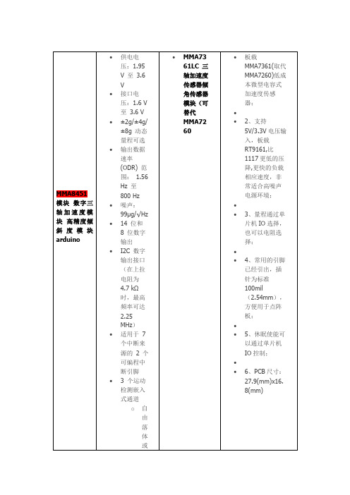
MMA8451模块数字三轴加速度模块高精度倾斜度模块arduino •供电电压:1.95V 至3.6V•接口电压:1.6 V至 3.6 V•±2g/±4g/±8g 动态量程可选•输出数据速率(ODR) 范围: 1.56Hz 至800 Hz•噪声:99μg/√Hz•14 位和8 位数字输出•I2C 数字输出接口(在上拉电阻为4.7 kΩ时,最高频率可达2.25MHz)•适用于7个中断来源的 2 个可编程中断引脚• 3 个运动检测嵌入式通道o自由落体或•MMA7361LC 三轴加速度传感器倾角传感器模块(可替代MMA7260•板载MMA7361(取代MMA7260)低成本微型电容式加速度传感器;••2、支持5V/3.3V电压输入,板载RT9161,比1117更低的压降,更快的负载相应速度,非常适合高噪声电源环境;••3、量程通过单片机IO选择,也可以电阻选择;••4、常用的引脚已经引出,插针为标准100mil(2.54mm),方便用于点阵板;••5、休眠使能可以通过单片机IO控制;••6、PCB尺寸:27.9(mm)x16.8(mm)。
buck电路lcd缓冲电路工作原理

一、概述在电子设备中,LCD(Liquid Crystal Display)液晶显示屏已经成为一种常见的显示技术。
而在LCD的驱动电路中,缓冲电路的作用十分重要。
本文将介绍在LCD驱动电路中常见的缓冲电路——buck电路的工作原理。
二、LCD驱动电路概述1. LCD显示屏原理LCD显示屏通过在液晶材料中施加电场来控制光的透过程度,从而显示出不同的图案和文字。
其驱动电路通常由更替的开关电源和缓冲电路组成,以便精确控制电场的幅度和方向。
2. 缓冲电路的重要性在LCD的驱动电路中,缓冲电路的作用是将输入信号的阻抗转换为适合驱动LCD的输出阻抗。
缓冲电路还能提供电流放大和隔离的功能,以保护LCD显示屏和驱动电路。
三、buck电路的基本原理1. buck电路概述buck电路是一种DC-DC转换电路,其工作原理是通过开关管的不断连接和断开,将输入电压稳定降低到所需的输出电压。
在LCD驱动电路中,buck电路常常被用来为显示屏提供稳定的电压。
2. buck电路的工作原理buck电路中包含一个功率开关、电感、电容和二极管。
当功率开关闭合时,电感带动电流增大,储存能量;当功率开关断开时,电感释放能量,输出电压减小。
通过不断地调整开关管的闭合时间,buck电路可以将输入电压稳定地降低到所需的输出电压。
四、LCD驱动电路中的buck电路应用1. buck电路的稳压特性在LCD驱动电路中,正常工作需要稳定的电压输出。
buck电路通过内置的反馈控制电路,能够对输入电压进行精确的调整,以获得稳定的输出电压。
2. buck电路的节能特性LCD作为电子设备中常见的显示技术,对功耗的要求很高。
buck电路能够高效地将输入电压转换为所需的输出电压,减少了电能的损耗,达到了节能的效果。
3. buck电路的稳定性和可靠性LCD在工作时需要稳定的电压输出,同时又要求对电源的质量要求较高。
buck电路能够满足LCD驱动电路对电压输出的稳定性和可靠性的要求,保证LCD工作的稳定和可靠。
HT8550 用户手册说明书
HT8550 用户手册钜泉光电科技(上海)股份有限公司目录1芯片概况 (9)1.1简介 (9)1.2基本特性 (9)1.3应用范围 (10)1.4系统框图 (10)1.5缩略语 (11)2引脚说明 (12)2.1引脚框图 (12)2.2引脚功能 (12)3电气规格 (14)3.1极限参数 (14)3.2电气特性 (14)4电源与时钟 (15)4.1电源系统 (15)4.2低功耗 (15)4.2.1门控时钟 (15)4.2.2时钟调整 (15)4.2.3MCU IDLE模式 (15)4.2.4MCU STOP模式 (16)4.2.5特殊功能寄存器 (16)4.3时钟系统 (17)4.3.1PLL时钟 (17)4.3.2时钟源选择和时钟分频 (17)4.3.3特殊功能寄存器 (18)4.4复位系统 (21)4.4.1上电/掉电复位 (21)4.4.2外部引脚复位 (22)4.4.3看门狗复位 (22)4.4.4软件复位 (22)4.4.5特殊功能寄存器 (22)5控制单元(MCU) (23)5.1MCU架构 (23)5.2存储单元 (23)5.2.1概述 (23)5.2.2片内资源访问 (24)5.2.3片外资源访问 (26)5.3DMA (26)5.3.1概况 (26)5.3.2DMA 操作流程 (26)5.3.3特殊功能寄存器 (26)5.4中断系统 (32)5.4.1概述 (32)5.4.2基于GPIO的中断 (33)5.4.3DMA中断 (33)5.4.4RTC中断 (33)5.4.5QMD中断 (33)5.4.6CC中断 (33)5.4.7掉电检测中断 (33)5.4.8中断列表 (33)5.4.9中断优先级 (34)5.4.10中断处理 (35)5.5定时器 (40)5.5.1概述 (40)5.5.2定时器0详细说明 (40)5.5.3定时器1详细说明 (41)5.5.4定时器2详细说明 (42)5.5.5特殊功能寄存器 (42)5.6GPIO (46)5.6.1特殊功能寄存器 (48)6其他外设 (49)6.1FLASH控制器 (50)6.1.1Flash 控制器简介 (50)6.1.2FLASH作为程序扩展 (50)6.1.3特殊功能寄存器 (50)6.2SPI接口 (53)6.2.1概述 (53)6.2.2主机模式 (54)6.2.3从机模式 (54)6.2.4特殊功能寄存器 (54)6.3I2C接口 (56)6.3.1概述 (56)6.3.2特殊功能寄存器 (57)6.4UART接口 (68)6.4.1概述 (68)6.4.2红外调制 (68)6.4.3UART0接口 (70)6.4.4UART1接口 (72)6.4.5特殊功能寄存器 (73)6.5RTC单元 (76)6.5.1概况 (76)6.5.2RTC开启和停止 (77)6.5.3RTC寄存器读写 (77)6.5.4RTC报警 (77)6.5.5特殊功能寄存器 (78)6.6看门狗定时器 (80)6.6.1概述 (80)6.6.2看门狗使能 (80)6.6.3看门狗计数器清零 (81)6.6.4特殊功能寄存器 (81)6.7JTAG调试 (81)7AFE相关寄存器配置 (81)7.1寄存器描述 (81)7.1.1ANALOG_CFG1 (82)7.1.2ANALOG_CFG2 (82)7.1.3VCC_LOSS (82)7.1.4AGC_LOOP_CFG1 (82)7.1.5AGC_LOOP_CFG2 (83)7.1.6AGC_LOOP_CFG3 (83)7.1.7AGC_LOOP_STATUS1 (83)7.1.8AGC_LOOP_STATUS2 (83)7.1.9ALC_CONTROL (84)7.2ALC功能描述 (84)7.3掉电检测 (84)7.4AGC的配置 (85)8.1概述 (85)8.2PHY功能简介 (85)8.3参数设置 (86)9芯片封装尺寸 (86)10附录 (86)10.1寄存器列表 (86)List of Tables表 1 缩略语 (11)表 2 引脚概述 (14)表 3 极限参数 (14)表 4 电气特性 (15)表 5 电源控制寄存器列表 (16)表 6 电源控制寄存器(PCON 0x87H) (16)表7 时钟模块表格 (18)表8 时钟相关寄存器列表 (19)表9 ADC和QMD时钟分频控制寄存器(ADC_QMD_CLK_CTRL 0xACH) (19)表10 外部Flash时钟分频控制寄存器(FLASH_CLK_DIV 0xD6H) (19)表11 时钟开启控制寄存器(CLK_ON 0xE5H) (20)表12 时钟开启控制寄存器(CLK_OFF 0xE6H) (20)表13 MAC时钟分频控制寄存器(MAC_CLK_DIV 0xF1H) (21)表14 时钟控制寄存器(CLK_CTRL 0xF2H) (21)表15 复位寄存器列表 (22)表16 复位设置寄存器(RST_SET 0xE7H) (23)表17 复位撤销寄存器(RST_CLR 0xE8H) (23)表18 内部数据存储器通用工作寄存器区 (25)表19 DMA寄存器列表 (27)表20 DMASEL寄存器描述(DMASEL 0xA1H) (27)表21 DMAS0寄存器描述(DMAS0 0xA2H) (27)表22 DMAS1寄存器描述(DMAS1 0xA3H) (28)表23 DMAS2寄存器描述(DMAS2 0xA4H) (28)表24 DMAS3寄存器描述(DMAS3 0xA5H) (28)表25 DMAT0寄存器描述(DMAT0 0xA6H) (28)表26 DMAT1寄存器描述(DMAT1 0xA7H) (28)表27 DMAT2寄存器描述(DMAT2 0xB1H) (28)表28 DMAT3寄存器描述(DMAT3 0xB2H) (28)表29 DMAC0寄存器描述(DMAC0 0xB3H) (29)表30 DMAC1寄存器描述(DMAC1 0xB4H) (29)表31 DMACSR寄存器描述(DMACSR 0xB5H) (30)表32 DMATC寄存器描述(DMA TC 0xB6H) (31)表33 DMASC寄存器描述(DMASC 0xB7H) (31)表34 MISC_PARAM寄存器描述(MISC_PARAM 0xA1H) (31)表35 MISC_ADDR寄存器描述(MISC_ADDR 0xA2H) (32)表36 CRC和扰码的表格 (32)表37 HT8550中断系统 (34)表38 中断优先级 (34)表39 中断优先级组成员 (35)表40 中断寄存器列表 (35)表41 IEN2寄存器描述(IEN2 0x9AH) (35)表42 IEN0寄存器描述(IEN0 0xA8H) (36)表43 IEN1寄存器描述(IEN1 0xB8H) (37)表44 IRCON寄存器描述(IRCON 0xC0H) (38)表45 MAC_INTR_MASK寄存器描述(MAC_INTR_MASK 0xFAH) (39)表46 GPIO_INTR_FLAGS寄存器描述(GPIO_INTR_FLAGS 0xFBH) (39)表47 PHY_INTR_FLAGS寄存器描述(PHY_INTR_FLAGS 0xFCH) (39)表48 定时器0和定时器1,定时器2寄存器列表 (42)表49 定时器0、定时器1控制寄存器(TCON 0x88H) (43)表50 定时器0、定时器1模式寄存器(TMOD 0x89H) (44)表51 定时器1状态寄存器(TH1 0x8DH) (44)HT8550 用户手册(V1.4)表52 定时器1状态寄存器(TL1 0x8BH) (44)表53 定时器0状态寄存器(TH0 0x8CH) (44)表54 定时器0状态寄存器(TL0 0x8AH) (45)表55 定时器2控制寄存器(T2CON 0xC8H) (45)表56 定时器2状态寄存器(TH2 0xCDH) (45)表57 定时器2状态寄存器(TL2 0xCCH) (46)表58 GPIO定义 (48)表59 GPIO寄存器列表 (48)表60 GPIO中断极性选择寄存器(GPIO_INTR_POLARITY 0xF9H) (49)表61 GPIO port选择寄存器(GPIO_MODE_SEL 0xFEH) (49)表62 GPIO 模式选择寄存器(GPIO_CTRL 0xFFH) (49)表63 FLASH控制器寄存器列表 (51)表64 Flash控制寄存器(FLASH_CTRL 0x8FH) (51)表65 Flash数据寄存器(FLASH_DATA 0x91H) (51)表66 Flash状态寄存器(FLASH_STATUS 0x96H) (52)表67 Flash复制寄存器(FLASH_COPY 0xABH) (52)表68 Flash页复制寄存器(FLASH_COPY_PAGES 0xBEH) (52)表69 Flash异或寄存器(Flash Memory XOR 0xD5H) (53)表70 Flash存储编程锁定寄存器(Program Memory Lock 0xD7H) (53)表71 SPI相关寄存器列表 (54)表72 SPI控制寄存器(SPSTA 0xE1H) (55)表73 SPI状态寄存器(SPCON 0xE2H) (56)表74 SPI数据寄存器(SPDAT 0xE3H) (56)表75 SPI从机选择寄存器(SPSSN 0xE4H) (56)表76 I2C 时序特征 (57)表77 I2C寄存器列表 (58)表78 I2C数据寄存器(I2CDAT 0xDAH) (58)表79 I2C地址寄存器(I2CADR 0xDBH) (58)表80 I2C控制寄存器(I2CCON 0xDCH) (59)表81 I2C状态寄存器(I2CSTA 0xDDH) (59)表82 I2C Status in Master Transmitter Mode (61)表83 I2C Status in Master Receiver Mode (62)表84 I2C Status in slave Receiver Mode (65)表85 I2C Status in slave Transmitter Mode (67)表86 I2C Status - miscellaneous states (68)表87 红外相关寄存器 (69)表88 串口红外控制寄存器(UART_IR_CTRL 0xBCH) (69)表89 串口红外频分寄存器(UART_IR_DIV 0xBDH) (70)表90 UART0常用波特率 (70)表91 UART1常用波特率 (72)表92 UART寄存器列表 (74)表93 串口0控制寄存器(S0CON 0x98H) (74)表94串口0缓冲寄存器(S0BUF 0x99H) (75)表95 串口1控制寄存器(S1CON 0x9BH) (75)表96 串口1缓冲寄存器(S1BUF 0x9CH) (75)表97 串口1波特率发生器的重载值低位(S1RELL 0x9DH) (76)表98 串口0波特率发生器的重载值低位(S0RELL 0xAAH) (76)表99 串口0波特率发生器的重载值高位(S0RELH 0xBAH) (76)表100 串口1波特率发生器的重载值高位(S1RELH 0xBBH) (76)表101 AD 控制寄存器(ADCON 0xD8H) (76)表102 RTC寄存器列表 (78)表103 RTC选择寄存器(RTCSEL 0xCEH) (78)HT8550 用户手册(V1.4)表104 RTC数据寄存器(RTCDAT 0xCFH) (79)表105 RTC中断使能寄存器(IEN4 0xD1H) (79)表106 RTCC RTC时钟控制寄存器(RTCSEL=0x4) (80)表107 看门狗寄存器列表 (81)表108 看门狗加载寄存器(WDTREL 0x86H) (81)表109 模拟前端寄存器列表 (82)表110 ANALOG_CFG1寄存器(ANALOG_CFG1 0xF3H) (82)表111 ANALOG_CFG2寄存器(ANALOG_CFG2 0xC9H) (82)表112 VCC_LOSS寄存器(VCC_LOSS 0xBFH) (82)表113 AGC_LOOP_CFG1寄存器(AGC_LOOP_CFG1 0xF4H) (83)表114 AGC_LOOP_CFG2寄存器(AGC_LOOP_CFG2 0xF7H) (83)表115 AGC_LOOP_CFG3寄存器(AGC_LOOP_CFG3 0xF8H) (83)表116 AGC_LOOP_STA TUS1寄存器(AGC_LOOP_STATUS1 0xFDH) (83)表117 AGC_LOOP_STA TUS2寄存器(AGC_LOOP_STATUS2 0xD4H) (84)表118 ALC_CONTROL寄存器(ALC_CONTROL 0xAFH) (84)HT8550 用户手册(V1.4) List of Figures图 1 HT8550系统框图 (10)图 2 引脚分布图 (12)图 3 存储器空间(片内MCU访问) (24)图 4 内部数据存储器功能结构 (25)图 5 SPI数据输出帧格式 (54)图 6 I2C 输出时序 (57)图7 I2C 输入时序 (57)图8 I2C 协议 (57)图9 串口红外调制 (69)图10 UART0模式0的帧格式 (71)图11 UART0模式1发送帧格式 (71)图12 UART0模式2 帧格式 (71)图13 RTC框图 (77)图14 ALC框图 (84)图15 掉电检测功能示意图 (85)图16 交互帧结构图 (85)图17 LQFP48 package information(单位mm) (86)1芯片概况1.1简介HT8550是一款高性能电力线载波通信芯片,采用先进的数模混合设计技术与工艺,提供低功耗、高灵敏度、高抗干扰能力的电力线数据通信,可实现各种类型的数据传输及远程抄表应用。
SST38LF6401RT 4M ×16 CMOS Advanced Multi-Purpose F

SummaryThe SST38LF6401RT is a 4M ×16 CMOS Advanced Multi-Purpose Flash Plus (Advanced MPF+) upgraded for space applications. It is manufactured with SST proprietary, high-performance CMOS SuperFlash ® technology. The split-gate cell design and thick-oxide tunneling injector attain better reliability and manufacturability compared with alternate approaches. The SST38L-F6401RT writes (program or erase) with a 3.0V to 3.6V power supply. This device conforms to JEDEC standard pin assignments for ×16 memories.SST38LF6401RT Parallel Rad Tolerant Flash MemoryFeatures• Density: 64 Mbit• Read access time: 90 ns • Page size (bytes): 8• Temperature range: –55°C to +125°C • Endurance: 10,000 cycles • Organized as 4M ×16• Single voltage read and write operations : 3.0V to 3.6V • Superior reliability, endurance: up to 10,000 cycles mini-mum, greater than 100 years data retention•Low-power consumption (typical values at 5 MHz)• Active current: 4 mA (typical)• Standby current: 3 µA (typical)• Auto low-power mode: 3 µA (typical)• 128-bit unique ID• Security-ID feature, 256 word, user one-time programmable• Protection and security features, hardware boot block protection/WP# input• Hardware Reset Pin (RST#)•Fast read and page read access times: 90 ns page read access times, 4-word page read buffer• Latched address and data• Fast erase times: sector-erase time: 18 ms (typical), block-erase time: 18 ms (typical), chip-erase time: 40 ms (typical)• Erase-suspend/resume capabilities• Fast word and write-buffer programming times:• Word-program time: 7 µs (typical)• Write buffer programming time: 1.75 µs/word(typical)• 16-word write buffer• Automatic write timing: internal V pp generation• End-of-write detection, toggle bits, data# polling, ry/by# output• CMOS I/O compatibility• JEDEC standard, Flash EEPROM pinouts and command sets• Pin, uniform (32 KWord) and non-uniform (8 KWord) op-tions available, user-controlled individual block (32 KWord) protection, using software only methods • Password protection • CFI Compliant•Packages available: 48-lead TSOP ceramic or plasticThe Microchip name and logo, the Microchip logo and SuperFlash are registered trademarks of Microchip Technology Incorporated in the U.S.A. and other countries. All other trademarks mentioned herein are property of their respective companies.© 2020, Microchip Technology Incorporated. All Rights Reserved. 11/20 DS00003649AWhat is SuperFlash Technology?SuperFlash Technology is an innovative, highly reliable and versatile type of NOR Flash memory invented by Silicon Storage Technology (SST, which is owned by Microchip). SuperFlash memory is much more flexible and reliable than competing non-volatile memories. This technology utilizes a split-gate cell architecture which uses a robust thick-oxide process that requires fewer mask steps resulting in a lower-cost nonvolatile memory solution with excellent data retention and higher reliability.Advantages of SuperFlash Technology• Fast, fixed program and erase times (typical chip-erase time: 40 ms)• No pre-programming or verify required prior to erase (Results in significantly lower power consumption)• Superior reliability (10K cycles and 100 years data retention)• Inherent small sector size (4 KB erase sector vs. 64 KB), results in faster re-write operations and contributes to lowering overall power consumptionSpace Environment• Full wafer lot traceability• 48-lead hermetic ceramic dual flat package (CDFP)• Space-grade screening and qualification (QML and ESCC flow)• T otal ionizing dose: better than 50 Krad, (biased & unbiased) • Heavy ions and protons tested• Single event latch-up immune with a LET > 78 MeV .cm²/mg • Full SEU characterization• No SEU corruption up to 46 MeV .cm²/mgFunctional Block Diagram®。
RT9184A型号的双通道CMOS低功耗电源管理器说明书

1DS9184A-09 April 2011Featuresz Low Quiescent Current (Typically 440μA)z Guaranteed 500mA Output Currentz Low Dropout Voltage : 600mV at 500mAz Wide Operating Voltage Ranges : 2.8V to 5.5V z Ultra-Fast Transient Response z Tight Load and Line Regulation z Current Limiting Protection z Thermal Shutdown ProtectionzOnly low-ESR Ceramic Capacitors Required for Stabilityz Custom Voltage AvailablezRoHS Compliant and 100% Lead (Pb)-FreePin ConfigurationsApplicationsz CD/DVD-ROM, CD/RWz Wireless LAN Card/Keyboard/Mouse z Battery-Powered Equipment zXDSL RouterDual, Ultra-Fast Transient Response, 500mA LDO RegulatorOrdering InformationGeneral DescriptionThe RT9184A series are an efficient, precise dual-channel CMOS LDO regulator optimized for ultra-low-quiescent applications. Both regulator outputs are capable of sourcing 500mA of output current.The RT9184A's performance is optimized for CD/DVD-ROM,CD/RW or wireless communication supply applications.The RT9184A regulators are stable with output capacitors as low as 1μF. The other features include ultra low dropout voltage, high output accuracy, current limiting protection,and high ripple rejection ratio.The RT9184A regulators are available in fused SOP-8package. Key features include current limit, thermal shutdown, fast transient response, low dropout voltage,high output accuracy, current limiting protection, and high ripple rejection ratio.(TOP VIEW)SOP-8Note :zThe output 2 is designated to larger than or equal to output 1 in voltage code order below, i.e. V OUT2 ≥ V OUT1.For example, the part number of RT9184A-FNCS is assigned for 2.5V OUT1/3.3V OUT2, contrary to the part number of RT9184A-NFCS is opposite to the rule and doesn't exist in the system.Voltage Code for Both Outputs :2: 1.2V A: 2.0V K: 3.0V U: 4.0V 3: 1.3V B: 2.1V L: 3.1V V: 4.1V 4: 1.4V C: 2.2V M: 3.2V W: 4.2V : : : :9: 1.9V J: 2.9V T: 3.9V Z: 4.5VRichTek products are :` RoHS compliant and compatible with the current require-ments of IPC/JEDEC J-STD-020.`Suitable for use in SnPb or Pb-free soldering processes.VOUT1VIN1VOUT2VIN2GNDGND GND GND2DS9184A-09 April 2011Function Block DiagramTypical Application CircuitNote: To prevent oscillation, a 1μF minimum X7R or X5R dielectric is strongly recommended if ceramics are used as input/output capacitors. When using the Y5V dielectric,the minimum value of the input/output capacitance that can be used for stable over full operating temperature range is 3.3μF. (see Application Information Section for further details)V V OUT1V IN2V IN1VIN1VOUT1VIN2GNDVOUT23DS9184A-09 April 2011Absolute Maximum Ratings (Note 1)z Supply Input Voltage ------------------------------------------------------------------------------------------------6.5V zPower Dissipation, P D @ T A = 25°CSOP-8------------------------------------------------------------------------------------------------------------------0.625W zPackage Thermal Resistance (Note 2)SOP-8, θJA ------------------------------------------------------------------------------------------------------------160°C/W z Lead Temperature (Soldering, 10 sec.)-------------------------------------------------------------------------260°C z Junction T emperature -----------------------------------------------------------------------------------------------150°Cz Storage Temperature Range ---------------------------------------------------------------------------------------−65°C to 150°C zESD Susceptibility (Note 3)HBM (Human Body Mode)-----------------------------------------------------------------------------------------2kV MM (Machine Mode)------------------------------------------------------------------------------------------------200VElectrical CharacteristicsRecommended Operating Conditions (Note 4)z Supply Input Voltage ------------------------------------------------------------------------------------------------2.8V to 5.5V zJunction T emperature Range --------------------------------------------------------------------------------------−40°C to 125°C(V IN= V OUT + 1V, or V IN = 2.8V whichever is greater, C IN = 1μF, C OUT = 1μF, T A = 25°C , for each LDO unless otherwise specified)4DS9184A-09 April 2011 Note 1. Stresses listed as the above “Absolute Maximum Ratings ” may cause permanent damage to the device. These arefor stress ratings. Functional operation of the device at these or any other conditions beyond those indicated in the operational sections of the specifications is not implied. Exposure to absolute maximum rating conditions for extended periods may remain possibility to affect device reliability.Note 2. θJA is measured in the natural convection at T A = 25°C on a low effective thermal conductivity test board ofJEDEC 51-3 thermal measurement standard.Note 3. Devices are ESD sensitive. Handling precaution recommended.Note 4. The device is not guaranteed to function outside its operating conditions.Note 5. Regulation is measured at constant junction temperature by using a 20ms current pulse. Devices are tested for loadregulation in the load range from 1mA to 500mA.Note 6. The dropout voltage is defined as V IN -V OUT , which is measured when V OUT is V OUT(NORMAL) − 100mV.Note 7. Quiescent, or ground current, is the difference between input and output currents. It is defined by I Q = I IN - I OUT under noload condition (I OUT = 0mA). The total current drawn from the supply is the sum of the load current plus the ground pin current.5DS9184A-09 April 2011Typical Operating CharacteristicsOutput Voltage vs. Temperature3.23.253.33.353.4-50-25255075100125Temperature O u t p u tV o l t a g e (V )(°C)-40Quiescent Current vs. Temperature300350400450500-50-25255075100125Temperature Q u i e s c e n tC u r r e n t (u A ) (°C)-40Current Limit vs. Input Voltage70075080085090033.544.555.5Input Voltage (V)C u r r e n t L i m i t (m A )Current Limit vs. Temperature700750800850900-50-25255075100125Temperature C u r r e n t L i m i t (m A )(°C)-40Load Transient RegulationI O U T 1(100m A /D i v )V O U T 1(20m V /D i v )V O U T 2(20m V /D i v )Time (1ms/Div)V IN1 = V IN2 = 5V, C IN1 = C IN2 = 1uF(X7R)C OUT1 = C OUT2 = 1uF(X7R), I OUT2 = 0A≈≈Load Transient RegulationI O U T 2(100m A /D i v )V O U T 1(20m V /D i v )V O U T 2(20m V /D i v )Time (1ms/Div)V IN1 = V IN2 = 5V, C IN1 = C IN2 = 1uF(X7R)C OUT1 = C OUT2 = 1uF(X7R), I OUT1 = 0A≈≈≈≈6DS9184A-09 April 2011 Dropout Voltage vs. Output Current01002003004005006007008000100200300400500Output Current (mA)D r o p o u t V o l t a g e (m A )Range of Stable ESR0.010.1110100100200300400500Output Current (mA)O u t p u t Ca p a c i t o r E S R (Ω)Output NoiseO u t p u t N o i s e S i g n a l (u V )Time (1ms/Div)V IN1 = 5VI LOAD = 100mAC IN1 = 1uF C OUT1 = 1uF3042-2F = 10Hz to 100kHzLine Transient RegulationI n p u t V o l t a g eD e v i a t i o n (V )O u t p u t V ol t ag e D e v i a t i o n (m V )Time (1ms/Div)V IN1 = 3 to 4V V IN2 = 5V C IN1 = 10uF C OUT1 = 10uF3042-2Power Supply Rejection Ratio-60-50-40-30-20-100101001000100001000001000000Frequency (Hz)P S R R (d B )1k 10k 100k 1M7DS9184A-09 April 2011Application InformationLike any low-dropout regulator, the RT9184A requires input and output decoupling capacitors. The device is specifically designed for portable applications requiring minimum board space and smallest components. These capacitors must be correctly selected for good performance (see Capacitor Characteristics Section). Please note that linear regulators with a low dropout voltage have high internal loop gains which require care in guarding against oscillation caused by insufficient decoupling capacitance.Input CapacitorAn input capacitance of ≅1μF is required between the device input pin and ground directly (the amount of the capacitance may be increased without limit). The input capacitor MUST be located less than 1cm from the device to assure input stability (see PCB Layout Section). A lower ESR capacitor allows the use of less capacitance, while higher ESR type (like aluminum electrolytic) require more capacitance.Capacitor types (aluminum, ceramic and tantalum) can be mixed in parallel, but the total equivalent input capacitance/ESR must be defined as above to stable operation.There are no requirements for the ESR on the input capacitor, but tolerance and temperature coefficient must be considered when selecting the capacitor to ensure the capacitance will be ≅1μF over the entire operating temperature range.Output CapacitorThe RT9184A is designed specifically to work with very small ceramic output capacitors. The recommended minimum capacitance (temperature characteristics X7R or X5R) are 1μF to 4.7μF range with 10m Ω to 50m Ω range ceramic capacitors between each LDO output and GND for transient stability, but it may be increased without limit.Higher capacitance values help to improve transient.The output capacitor's ESR is critical because it forms a zero to provide phase lead which is required for loop stability. (When using the Y5V dielectric, the minimum value of the input/output capacitance that can be used for stable over full operating temperature range is 3.3μF.)No Load StabilityThe device will remain stable and in regulation with no external load. This is specially important in CMOS RAM keep-alive applications.Input-Output (Dropout) VoltageA regulator's minimum input-to-output voltage differential (dropout voltage) determines the lowest usable supply voltage. In battery-powered systems, this determines the useful end-of-life battery voltage. Because the device uses a PMOS, its dropout voltage is a function of drain-to-source on-resistance, R DS(ON), multiplied by the load current :V DROPOUT = V IN − V OUT = R DS(ON) × I OUT Current LimitThe RT9184A monitors and controls the PMOS' gate voltage, limiting the output current to 500mA (min.). The output can be shorted to ground for an indefinite period of time without damaging the part.Short-Circuit ProtectionThe device is short circuit protected and in the event of a peak over-current condition, the short-circuit control loop will rapidly drive the output PMOS pass element off. Once the power pass element shuts down, the control loop will rapidly cycle the output on and off until the average power dissipation causes the thermal shutdown circuit to respond to servo the on/off cycling to a lower frequency.Please refer to the section on thermal information for power dissipation calculations.Capacitor CharacteristicsIt is important to note that capacitance tolerance and variation with temperature must be taken into consideration when selecting a capacitor so that the minimum required amount of capacitance is provided over the full operating temperature range. In general, a good tantalum capacitor will show very little capacitance variation with temperature,but a ceramicmay not be as good (depending on dielectric type).Aluminum electrolytics also typically have large temperature variation of capacitance value.8DS9184A-09 April 2011 Equally important to consider is a capacitor's ESR change with temperature: this is not an issue with ceramics, as their ESR is extremely low. However, it is very important in tantalum and aluminum electrolytic capacitors. Both show increasing ESR at colder temperatures, but the increase in aluminum electrolytic capacitors is so severe they may not be feasible for some applications.Ceramic :For values of capacitance in the 10μF to 100μF range,ceramics are usually larger and more costly than tantalums but give superior AC performance for by-passing high frequency noise because of very low ESR (typically less than 10m Ω). However, some dielectric types do not have good capacitance characteristics as a function of voltage and temperature.Z5U and Y5V dielectric ceramics have capacitance that drops severely with applied voltage. A typical Z5U or Y5V capacitor can lose 60% of its rated capacitance with half of the rated voltage applied to it. The Z5U and Y5V also exhibit a severe temperature effect, losing more than 50%of nominal capacitance at high and low limits of the temperature range.X7R and X5R dielectric ceramic capacitors are strongly recommended if ceramics are used, as they typically maintain a capacitance range within ±20% of nominal over full operating ratings of temperature and voltage. Of course,they are typically larger and more costly than Z5U/Y5U types for a given voltage and capacitance.Tantalum :Solid tantalum capacitors are recommended for use on the output because their typical ESR is very close to the ideal value required for loop compensation. They also work well as input capacitors if selected to meet the ESR requirements previously listed.Tantalums also have good temperature stability: a good quality tantalum will typically show a capacitance value that varies less than 10~15% across the full temperature range of 125°C to -40°C. ESR will vary only about 2X going from the high to low temperature limits.The increasing ESR at lower temperatures can cause oscillations when marginal quality capacitors are used (if the ESR of the capacitor is near the upper limit of the stability range at room temperature).Aluminum :This capacitor type offers the most capacitance for the money. The disadvantages are that they are larger in physical size, not widely available in surface mount, and have poor AC performance (especially at higher frequencies) due to higher ESR and ESL.Compared by size, the ESR of an aluminum electrolytic is higher than either T antalum or ceramic, and it also varies greatly with temperature. A typical aluminum electrolytic can exhibit an ESR increase of as much as 50X when going from 25°C down to -40°C.It should also be noted that many aluminum electrolytics only specify impedance at a frequency of 120Hz, which indicates they have poor high frequency performance. Only aluminum electrolytics that have an impedance specified at a higher frequency (between 20kHz and 100kHz) should be used for the device. Derating must be applied to the manufacturer's ESR specification, since it is typically only valid at room temperature.Any applications using aluminum electrolytics should be thoroughly tested at the lowest ambient operating temperature where ESR is maximum.PCB LayoutGood board layout practices must be used or instability can be induced because of ground loops and voltage drops.The input and output capacitors MUST be directly connected to the input, output, and ground pins of the device using traces which have no other currents flowing through them.The best way to do this is to layout C IN and C OUT near the device with short traces to the V IN , V OUT , and ground pins.The regulator ground pin should be connected to the external circuit ground so that the regulator and its capacitors have a “single point ground ”.9DS9184A-09 April 2011SOP-8 Board LayoutGNDV IN2GNDGNDV IN1V OUT1V OUT2It should be noted that stability problems have been seen in applications where “vias ” to an internal ground plane were used at the ground points of the device and the input and output capacitors. This was caused by varying ground potentials at these nodes resulting from current flowing through the ground plane. Using a single point ground technique for the regulator and it's capacitors fixed the problem. Since high current flows through the traces going into V IN and coming from V OUT , Kelvin connect the capacitor leads to these pins so there is no voltage drop in series with the input and output capacitors.Optimum performance can only be achieved when the device is mounted on a PC board according to the diagram below :10DS9184A-09 April 2011Information that is provided by Richtek Technology Corporation is believed to be accurate and reliable. Richtek reserves the right to make any change in circuit design, specification or other related things if necessary without notice at any time. No third party intellectual property infringement of the applications should be guaranteed by users when integrating Richtek products into any application. No legal responsibility for any said applications is assumed by Richtek.Richtek Technology CorporationHeadquarter5F, No. 20, Taiyuen Street, Chupei City Hsinchu, Taiwan, R.O.C.Tel: (8863)5526789 Fax: (8863)5526611Richtek Technology CorporationTaipei Office (Marketing)5F, No. 95, Minchiuan Road, Hsintien City Taipei County, Taiwan, R.O.C.Tel: (8862)86672399 Fax: (8862)86672377Email:*********************Outline DimensionHM8-Lead SOP Plastic Package。
SiC431, SiC437, SiC438 Reference Board User’s Manu

Reference Board User’s ManualHigh Voltage Synchronous Buck Regulators: 3 V to 24 VSiC431 (24 A), SiC437 (12 A), SiC438 (8 A)DESCRIPTIONThe SiC431/437/438 is family of synchronous buck regulators with integrated high side and low side power MOSFETs. Its power stage is capable of supplying up to 24 A continuous current at 1 MHz switching frequency. This regulator produces an adjustable output voltage down to 0.6 V from 3 V to 24 V input rail to accommodate a variety of applications, including computing, consumer electronics,telecom, and industrial. SiC43x series employs a constant ON time control architecture that supports ultrafast transient response with minimum output capacitance and tight ripple regulation at very light load. The device is internally compensated and no external ESR network is required for loop stability purposes. The device also incorporates a power saving scheme that significantly increases light load efficiency. The regulator integrates a full protection feature set, including output over voltage protection (OVP), cycle by cycle over current protection (OCP) short circuit protection (SCP) and thermal shutdown (OTP). It also has UVLO and a user programmable soft start. The SiC43x series is available in lead (Pb)-free power enhanced MLP44-24L package in 4 mm x 4 mm dimension.FEATURES•Versatile- Single supply operation from 3 V to 24 V input voltage -Adjustable output voltage down to 0.6 V - Scalable solution8 A (SiC438), 12 A (SiC437), 24 A (SiC431)- Output voltage tracking and sequencing with pre-bias start up- ± 1 % output voltage accuracy at -40 °C to +125 °C •Highly efficient - 97 % peak efficiency- 1 μA supply current at shutdown - 50 μA operating current not switching •Highly configurable-Four programmable switching frequencies available:300 kHz, 500 kHz, 750 kHz, and 1 MHz - Adjustable soft start and adjustable current limit - 3 modes of operation: forced continuous conduction,power save, or ultrasonic •Robust and reliable- Cycle-by-cycle current limit - Output overvoltage protection- Output undervoltage / short circuit protection with auto retry - Power good flag and over temperature protection •Design tools- Supported by Vishay PowerCAD Online Design Simulation (/power-ics/powercad-list/)- Design support kit (/ppg?74589)•Material categorization: for definitions of compliance please see /doc?99912APPLICATIONS•Industrial and automation •Home automation•Industrial and server computing•Networking, telecom, and base station power supplies •Wall transformer regulation •Robotics•High end hobby electronics: remote control cars, planes,and drones•Battery management systems •Power tools•Vending, ATM, and slot machinesORDERING TABLEPART NUMBER MODEOUTPUT CURRENTSiC431AEVB-A Ultrasonic24 A SiC431BEVB-APower safe 24 ASiC437AEVB-BUltrasonic 12 A SiC437BEVB-BPower safe12 A SiC438AEVB-B Ultrasonic 8 A SiC438BEVB-BPower safe8 ASPECIFICATIONSThis reference board allows the end user to evaluate the SiC43x series microBUCK® regulators for their features and functionalities. The user may also change the operating range may be modified by making changes to the jumper connections. See section “Selection Jumpers” below in the document.CONNECTION AND SIGNAL / TEST POINTS Power Terminals (J10)- +V IN (pin 1), V IN GND (pin 2)Connect to a voltage source to this pin. The minimum input voltage will be 3 V. For input voltages (V IN) below 4.5 V an external V DD and V DRD is required.- +V OUT (pins 5 and 6), V OUT GND (pins 3 and 4)Fig. 1 - SiC43x EVBSELECTION JUMPERSMode SelectJ1, to J8 and J15: there are 4 jumpers which allow the user to select one of four modes of operation.J1 to J4 to select switching frequency: 300 kHz to 1 MHz. Short pins 1 and 2 for PSM mode, short pins 2 and 3 for FCCM modeJ5 to J8 to select over current trip (I LIM). Short pins 1 and 3 to select 6 mS soft start, short pins 2 and 3 to select 6 mS soft startJ15 to select output voltage: 1 V, 3.3 V, 5 V and 12 V EnableJ9: this is the jumper that enables/disables the part.With J9 left open, the device is enabled, via R9 to V IN+. To disable the part, short J9.SIGNALS AND TEST LEADSInput Voltage SenseV IN_SENSE (TP11), GND IN_SENSE (TP12): this allows the user to measure the voltage directly at the input of the regulator bypassing any losses generated by connections to the board. These test points can also be as a remote sense port of a power source with remote sense capability.Output Voltage SenseV OUT_SENSE (TP13), GND OUT_SENSE (TP14): this allows the user to measure the output voltage directly at the sense point of the regulator bypassing any losses generated by connections to the board. These test points can also be as a remote sense port of an external load with remote sense capability.Power Good IndicatorPGD (J17): is an open drain output and is pulled up with a 100 kΩ resistor, R12, to V DD1 (≈ 5 V). When FB or V OUT are within -10 % to +20 % of the set voltage this pin will go HI to indicate the output is okay. To prevent false triggering during transient events, the P GOOD has a 25 μS blanking time.Power Up ProcedureBefore turning on the reference board, the user needs to select one of the three modes by shorting one jumper (see section on mode selection). It is recommend to disable theSiC431 before making any changes to the jumpers.SCHEMATIC FOR SiC431SCHEMATIC FOR SiC437, SiC438SCHEMATIC, DESIGN, BILL OF MATERIALS, AND GERBER FILES FOR PCB FABRICATIONThese files are as follows:•“*.DSN” for schematic design file•“*.DBK” for data backup file for Orcad•“.opj” Orcad project file. Any schematic work should always be opened with the opj file. Use of a DSN file for this purpose is not advised•“*.xlsx” is the bill of materials (BOM) derived from the schematic•“*.PDF” is the PDF version of the schematic from the “*.DSN” fileThe Fab files for the high power and low power are located in a separate sub directory and contain gerbers,.brd files (Allegro), etc. for PCB fabrication.PCB LAYOUT FOR SiC431Fig. 2 - Top LayerFig. 3 - Inner Layer 2Fig. 4 - Inner Layer 3Fig. 5 - Inner Layer 4 Fig. 6 - Inner Layer 5Fig. 7 - Bottom LayerPCB LAYOUT FOR SiC437, SiC438Fig. 8 - Top LayerFig. 9 - Inner Layer 2Fig. 10 - Inner Layer 3Fig. 11 - Inner Layer 4 Fig. 12 - Inner Layer 5Fig. 13 - Bottom LayerBILL OF MATERIAL REPORT, SiC431SYM_NAME COMP_VALUE REFDES PART NUMBER 04020.1 μF C1, C5, C6GRM155R71H104ME14D 121022 μF C2, C3, C4CL32B226KAJNFNE 0603 1 μF C7GCM188R71E105KA64D POSCAP100 μF C8, C920TQC100MYF0603DNP C10121022 μF C11, C12, C13, C14CL32B226KAJNFNEDNP C15, C16, C1706030.1 μF C18GCM188R71E104KA57D CAP10P2x5220 μF C20UBT1E221M SiC431SiC431IC1MINIJUMPER3CON3J1, J2, J3, J4, J5, J6, J7, J8, J9M50-3530342 CON6CON6J10277-1581-NDTP30VIN+s J1136-5000-NDTP30VIN-S J1236-5001-NDTP30VO+S J1336-5000-NDTP30VO-S J1436-5001-ND MINIJUMPER2x4CON8A J15S9015E-04-ND TP30AGND J1636-5001-NDTP30PGOOD J1736-5002-NDDNP L1IHLP 1 μH L2ZPWM-101014MA-1R0K 040251k R1, R5CRCW040251K0FKED 0402100k R2, R6, R9, R12CRCW0402100KFKED 0402200k R3, R7CRCW0402200KFKED 0402510k R4, R8CRCW0402510KFKED 04020R10CRCW04020000Z0ED 060310k R11TNPW060310K0BXEN 0603 6.65k R14TNPW06036K65BEEA 060345.3k R15TNPW060345K3BEEA 060373.2k R16TNPW060373K2BEEA 0603191k R17TNPW0603191KBEEA 1206DNP R18JUMPER OFF BOARD x3NPB02SVFN-RCBILL OF MATERIAL REPORT, SiC437, SiC438SYM_NAME COMP_VALUE REFDES PART NUMBER 04020.1 μF C1, C5, C6GRM155R71H104ME14D121022 μF C2, C3, C4CL32B226KAJNFNE0603 1 μF C7GCM188R71E105KA64DPOSCAP100 μF C8, C920TQC100MYF0603DNP C10121022 μF C13, C14CL32B226KAJNFNEDNP C11, C12, C15, C16, C1706030.1 μF C18GCM188R71E104KA57DSiC437/8SiC437/8IC1MINIJUMPER3CON3J1, J2, J3, J4, J5, J6, J7, J8,J 9M50-3530342 CON6CON6J10277-1581-NDTP30VIN+s J1136-5000-NDTP30VIN-S J1236-5001-NDTP30VO+S J1336-5000-NDTP30VO-S J1436-5001-ND MINIJUMPER2x4CON8A J15S9015E-04-ND TP30AGND J1636-5001-NDTP30PGOOD J1736-5002-NDDNP L1DNP L1IHLP 2.2 μH L2 (for SiC437x)IHLP4040DZER2R2M01IHLP 3.3 μH L2 (for SiC438x)IHLP4040DZER3R3M5A040251k R1, R5CRCW040251K0FKED0402100k R2, R6, R9, R12CRCW0402100KFKED0402200k R3, R7CRCW0402200KFKED0402510k R4, R8CRCW0402510KFKED04020R10CRCW04020000Z0ED060310k R11TNPW060310K0BXEN0603 6.65k R14TNPW06036K65BEEA060345.3k R15TNPW060345K3BEEA060373.2k R16TNPW060373K2BEEA0603191k R17TNPW0603191KBEEA1206DNP R18JUMPER OFF BOARD x3NPB02SVFN-RCVishay Siliconix maintains worldwide manufacturing capability. Products may be manufactured at one of several q ualified locations. Reliability data for Silicon Technology and Package Reliability represent a composite of all qualified locations. For related documents such as package / tape drawings, part marking, and reliability data, see /ppg?76801.。