IGBT说明书
微机励磁控制器说明书
GDF-2微机励磁控制器(GDF-IGBT)安装使用说明深圳市国立旭振电气技术有限公司一、概述GDF-系列励磁控制器只需要一键启动后,即可实现励磁控制全自动,无人值守运行!▲GDF-系列励磁控制器是2014最新版。
IGBT励磁控制技术为目前较为先进的直流控制技术,现在国内只有少数励磁制造厂家掌握并用于高端励磁控制系统(高压励磁控制系统),原因是技术要求高、制造成本高。
我们将IGBT技术首先用于无刷励磁发电机。
解决了可控硅励磁容易受中频干扰,在满负荷跳闸时失压,无法为向水机提供关机电源等难题。
▲电路板制造时采用元件贴片技术,大大减少了人工插件制作的错误。
解决或修正了旧版本的已知问题。
主要特别功能:1、并网后自动按设定的功率因数值运行。
2、IGBT模块智能控制,不受谐波干扰,可以在180V以下的励磁电压稳定运行。
3、励磁控制回路手动调试功能,方便用户对控制器检查、设置和对发电机充磁。
4、发电机电压恒定、电压快速恢复功能,防止过电压或低电压。
5、自动识别停机过程并进行可调整的灭磁频率控制。
6、“独立小电网运行”功能,通过软件设置可实现该功能,适合工厂自行组合小电网的柴油发电机组并列运行。
7、50HZ或60HZ运行频率适应功能。
8、防止发电机过负荷功能。
二、技术参数1. 适用范围:▲GDF-IGBT适用于励磁电流15A以下、励磁电压180V以下的无刷励磁发电机。
2. 输入信号:▲电流:串接发电机定子C相电流互感器电流,额定电流:5A。
▲电压:发电机A1、B1、N电压400V/230V,电网A2、B2电压400V。
▲并网识别:发电机出口断路器的辅助接点:常开接点。
3. 控制器输出:励磁输出电压串电流表后至发电机的励磁电机。
4. 环境温度: -10°C~+50°C 海拔:2500米以下地区5.外型尺寸:控制器(宽)305 mm×(高)146 mm×(深)240mm6. 开孔尺寸:(宽)264 mm×(高)124 mm(GDF系列全部相同)三、安装接线1、阅读理解接线原理图,按端子接线图接好外引连线。
IXA12IF1200PB IGBT模块说明书

Copack
Part number
IXA12IF1200PB
IXA12IF1200PB
VCES =
I C25
=
V = CE(sat)
preliminary
1200 V 20 A 1.8 V
(G) 1
2 (C) 3 (E)
Backside: collector
Features / Advantages:
* on die level
IGBT
1.1 153
T VJ = 150 °C
Diode
1.25
V
85 mΩ
IXYS reserves the right to change limits, conditions and dimensions.
© 2011 IXYS all rights reserved
● Thin wafer technology combined with the XPT design results in a competitive low VCE(sat)
● SONIC™ diode - fast and soft reverse recovery - low operating forward voltage
IXA12IF1200PB
preliminary
Conditions
IC = 10A; VGE = 15 V IC = 0.3mA; VGE = VCE VCE = VCES; VGE = 0 V VGE = ±20 V VCE = 600 V; VGE = 15 V; IC =
inductive load VCE = 600 V; IC = 10 A VGE = ±15 V; RG=100 Ω
IGBT驱动板IGQD4使用手册说明书

IGBT 驱动板IGQD4使 用 手 册VER10产品安装,使用之前请认真阅读本使用手册.请妥善保管好本手册以备今后参阅株洲市华维变流数控设备有限公司地址地址::湖南省株洲市石峰区红旗北路186号 邮编邮编邮编::412004120011 电话电话::07310731--28436893 0738436893 07311-22967089 967089 138138138--07336044 07336044 传真传真::07307311-2262605939 05939 05939 E E -mail:mail:huaweiacdc huaweiacdc huaweiacdc@126.@126.@ net net 网站网站:: http://www.China http://www.Chinaa a c d net net1.概述概述绝缘栅双极晶体管(IGBT)是80 年代出现的新型复合器件。
其响应速度快,工作电流大, 耐压高等优点使得它在开关电源、变频器、逆变器等领域里很受青睐。
但由于IGBT 自身的特性, 使其工作时会发生擎住效应而导致门极失控, 或者因电流电压过大或不稳定, 造成IGBT 损坏而不能正常工作。
为此,对IGBT 的驱动和保护(特别是短路过流保护) 提出了很高的要求。
IGBT 的驱动电路的形式很多, 为了提高可靠性, 我们在此采用专用驱动模块M57962AL来驱动,它能驱动大电流大功率的应用, 能实现对IGBT的过流过压保护, 同时, 所设计的外围应用电路采用限制基极限流电阻和基射极限幅器, 确保了IGBT 基极不被烧坏和击穿。
主应用于逆变器、不间断电源、变频器、电焊机、伺服系统。
2.产品名称及型号名称:高频IGBT驱动板(4单元)。
型号:IGQD4。
3.IGBT驱动板产品特点四单元驱动板,驱动功率大, 可以驱动600A/600V 或400A/1200V的IGBT模块。
半桥应用时,双管信号互锁,用户可以设置死区时间,确保不直通。
高压 IGBT 数据手册说明书

HGTG18N120BND1200 V NPT IGBTHGTG18N120BND is based on Non- Punch Through (NPT)IGBT designs. The IGBT is ideal for many high voltage switching applications operating at moderate frequencies where lowconduction losses are essential, such as: UPS, solar inverter, motor control and power supplies.Formerly Developmental Type TA49304.Ordering InformationPART NUMBER PACKAGE BRANDHGTG18N120BNDTO-24718N120BNDNOTE: When ordering, use the entire part number.SymbolEGCFeatures•26 A, 1200 V , T C = 110°C•Low Saturation V oltage: V CE (sat) = 2.45 V @ I C = 18 A •Typical Fall Time . . . . . . . . . . . . . 140ns at T J = 150°C •Short Circuit Rating •Low Conduction LossPackagingJEDEC STYLE TO-247TO-247GCEAbsolute Maximum Ratings T C = 25o C, Unless Otherwise SpecifiedHGTG18N120BND UNIT Collector to Emitter V oltage. . . . . . . . . . . . . . . . . . . . . . . . . . . . . . . . . . . . . . . . . . . . . . . . . . . . .BV CES1200V Collector Current ContinuousAt T C = 25o C . . . . . . . . . . . . . . . . . . . . . . . . . . . . . . . . . . . . . . . . . . . . . . . . . . . . . . . . . . . . . . . . I C2554AAt T C = 110o C . . . . . . . . . . . . . . . . . . . . . . . . . . . . . . . . . . . . . . . . . . . . . . . . . . . . . . . . . . . . . . I C11026A Collector Current Pulsed (Note 1) . . . . . . . . . . . . . . . . . . . . . . . . . . . . . . . . . . . . . . . . . . . . . . . . . . I CM160AGate to Emitter V oltage Continuous. . . . . . . . . . . . . . . . . . . . . . . . . . . . . . . . . . . . . . . . . . . . . . . .V GES±20VGate to Emitter V oltage Pulsed. . . . . . . . . . . . . . . . . . . . . . . . . . . . . . . . . . . . . . . . . . . . . . . . . . . V GEM±30V Switching Safe Operating Area at T J = 150o C (Figure 2) . . . . . . . . . . . . . . . . . . . . . . . . . . . . . . .SSOA100A at 1200VPower Dissipation Total at T C = 25o C. . . . . . . . . . . . . . . . . . . . . . . . . . . . . . . . . . . . . . . . . . . . . . . . P D390WPower Dissipation Derating T C > 25o C. . . . . . . . . . . . . . . . . . . . . . . . . . . . . . . . . . . . . . . . . . . . . . . . . . 3.12W/o C Operating and Storage Junction Temperature Range . . . . . . . . . . . . . . . . . . . . . . . . . . . . . . . . T J, T STG-55 to 150o C Maximum Lead Temperature for Soldering. . . . . . . . . . . . . . . . . . . . . . . . . . . . . . . . . . . . . . . . . . . . T L260o CShort Circuit Withstand Time (Note 2) at V GE = 15V. . . . . . . . . . . . . . . . . . . . . . . . . . . . . . . . . . . . t SC8μsShort Circuit Withstand Time (Note 2) at V GE = 12V. . . . . . . . . . . . . . . . . . . . . . . . . . . . . . . . . . . . t SC15μs CAUTION: Stresses above those listed in “Absolute Maximum Ratings” may cause permanent damage to the device. This is a stress only rating and operation of the device at these or any other conditions above those indicated in the operational sections of this specification is not implied.NOTES:Pulse width limited by maximum junction temperature.1.V2.CE(PK) = 960V, T J = 125o C, R G = 3Ω.Electrical Specifications T C = 25o C, Unless Otherwise SpecifiedPARAMETER SYMBOL TEST CONDITIONS MIN TYP MAX UNIT Collector to Emitter Breakdown Voltage BV CES I C = 250μA, V GE = 0V1200--V Emitter to Collector Breakdown Voltage BV ECS I C = 10mA, V GE = 0V15--V Collector to Emitter Leakage Current I CES V CE = 1200V T C = 25o C--250μAT C = 125o C-300-μAT C = 150o C--4mACollector to Emitter Saturation Voltage V CE(SAT)I C = 18A,V GE = 15V T C = 25o C- 2.45 2.7V T C = 150o C- 3.8 4.2VGate to Emitter Threshold Voltage V GE(TH)I C = 150μA, V CE = V GE 6.07.0-V Gate to Emitter Leakage Current I GES V GE = ±20V--±250nA Switching SOA SSOA T J = 150o C, R G = 3Ω, V GE = 15V,L = 200μH, V CE(PK) = 1200V100--A Gate to Emitter Plateau Voltage V GEP I C = 18A, V CE = 600V-10.5-VOn-State Gate Charge Q G(ON)I C = 18A,V CE = 600V V GE = 15V-165200nC V GE = 20V-220250nCCurrent Turn-On Delay Time t d(ON)I IGBT and Diode at T J = 25o CI CE = 18AV CE = 960VV GE = 15VR G = 3ΩL = 1mHTest Circuit (Figure 20)-2328nsCurrent Rise Time t rI-1722ns Current Turn-Off Delay Time t d(OFF)I-170200ns Current Fall Time t fI-90140ns Turn-On Energy E ON- 1.9 2.4mJ Turn-Off Energy (Note 3)E OFF- 1.8 2.2mJCurrent Turn-On Delay Time t d(ON)I IGBT and Diode at T J = 150o C I CE = 18A V CE = 960V V GE = 15V R G = 3Ω L = 1mHTest Circuit (Figure 20)-2126ns Current Rise Timet rI -1722ns Current Turn-Off Delay Time t d(OFF)I -205240ns Current Fall Time t fI -140200ns Turn-On Energy E ON - 3.7 4.9mJ Turn-Off Energy (Note 3)E OFF - 2.6 3.1mJ Diode Forward Voltage V EC I EC = 18A- 2.6 3.2V Diode Reverse Recovery Timet rrI EC = 18A, dI EC /dt = 200A/μs -6075ns I EC = 2A, dI EC /dt = 200A/μs-4455nsThermal Resistance Junction To CaseR θJCIGBT --0.32o C/W Diode--0.75o C/WNOTE:3. Turn-Off Energy Loss (E OFF ) is defined as the integral of the instantaneous power loss starting at the trailing edge of the input pulse and ending at the point where the collector current equals zero (I CE = 0A). All devices were tested per JEDEC Standard No. 24-1 Method for Measurement of Power Device Turn-Off Switching Loss. This test method produces the true total Turn-Off Energy Loss.Electrical SpecificationsT C = 25o C, Unless Otherwise Specified (Continued)PARAMETERSYMBOL TEST CONDITIONSMIN TYP MAX UNIT Typical Performance Curves Unless Otherwise SpecifiedFIGURE 1. T C , CASE TEMPERATURE (o C)I C E , D C C O L L E C T O R C U R R E N T (A )50602575100125150********V GE = 15V50DC COLLECTOR CURRENT vs CASETEMPERATUREFIGURE 2. V CE , COLLECTOR TO EMITTER VOLTAGE (V)1400800I C E , C O L L E C T O R T O E M I T T E R C U R R E N T (A )204060080040020010001200010012060T J = 150o C, R G = 3Ω, V GE = 15V , L = 200μHMINIMUM SWITCHING SAFE OPERATING AREAFIGURE 3. I CE , COLLECTOR TO EMITTER CURRENT (A)T J = 150o C, R G = 3Ω, L = 1mH, V CE = 960Vf M A X , O P E R A T I N G F R E Q U E N C Y (k H z )51104020501010030T C = 75o C, V GE = 15V , IDEAL DIODEf MAX1 = 0.05 / (t d(OFF)I + t d(ON)I )R ØJC = 0.32o C/W, SEE NOTES P C = CONDUCTION DISSIPATION (DUTY FACTOR = 50%)f MAX2 = (P D - P C ) / (E ON + E OFF )T CV GE110o C 12V15V 15V 75o C110o C75o C12V OPERATING FREQUENCY vs COLLECTOR TOEMITTER CURRENTFIGURE 4. V GE , GATE TO EMITTER VOLTAGE (V)I S C , P E A K S H O R T C I R C U I T C U R R E N T (A )t S C , S H O R T C I R C U I T W I T H S T A N D T I M E (μs )121314151651015202550100150200300t SCI SC30250V CE = 960V , R G = 3Ω, T J = 125o CSHORT CIRCUIT WITHSTAND TIMEFIGURE 5. 024V CE , COLLECTOR TO EMITTER VOLTAGE (V)I C E , C O L L E C T O R T O E M I T T E R C U R R E N T (A )0204068106080PULSE DURATION = 250μsDUTY CYCLE < 0.5%, V GE = 12V T C = -55o CT C = 25o CT C = 150o CCOLLECTOR TO EMITTER ON-STATE VOLTAGEFIGURE 6. I C E , C O L L E C T O R T O E M I T T E R C U R R E N T (A )V CE , COLLECTOR TO EMITTER VOLTAGE (V)406080246810201000T C = -55o CT C = 25o CT C = 150o CDUTY CYCLE < 0.5%, V GE = 15V PULSE DURATION = 250μsCOLLECTOR TO EMITTER ON-STATE VOLTAGEFIGURE 7. E O N 2, T U R N -O N E N E R G Y L O S S (m J )106I CE , COLLECTOR TO EMITTER CURRENT (A)8421510512253003540T J = 25o C, V GE = 12V , V GE = 15VT J = 150o C, V GE = 12V , V GE = 15VR G = 3Ω, L = 1mH, V CE = 960V 20TURN-ON ENERGY LOSS vs COLLECTOR TOEMITTER CURRENT FIGURE 8. 3.5I CE , COLLECTOR TO EMITTER CURRENT (A)E OF F , T U R N -O F F E N E RG Y L O S S (m J )0.5151051.02.51.53.04.04.52530R G = 3Ω, L = 1mH, V CE = 960VT J = 25o C, V GE = 12V OR 15VT J = 150o C, V GE = 12V OR 15V35402.020TURN-OFF ENERGY LOSS vs COLLECTOR TOEMITTER CURRENTFIGURE 9. I CE , COLLECTOR TO EMITTER CURRENT (A)t d I ,T U R N -O N D E L A Y T I M E (n s )5101520253035154025303540R G = 3Ω, L = 1mH, V CE = 960VT J = 25o C, T J = 150o C, V GE = 12VT J = 25o C, T J = 150o C, V GE = 15V20TURN-ON DELAY TIME vs COLLECTOR TOEMITTER CURRENTFIGURE 10. I CE , COLLECTOR TO EMITTER CURRENT (A)t r I ,R I S E T I M E (n s )100208060305402520154035100120R G = 3Ω, L = 1mH, V CE = 960VT J = 25o C, T J = 150o C, V GE = 12VT J = 25o C OR T J = 150o C, V GE = 15V TURN-ON RISE TIME vs COLLECTOR TOEMITTER CURRENTFIGURE 11. 1020520015100150I CE , COLLECTOR TO EMITTER CURRENT (A)t d (O F F )I , T U R N -O F F D E L A Y T I M E (n s )303502503004035R G = 3Ω, L = 1mH, V CE = 960V25V GE = 12V , V GE = 15V , T J = 25o CV GE = 12V , V GE = 15V , T J = 150o CTURN-OFF DELAY TIME vs COLLECTOR TOEMITTER CURRENT FIGURE 12. I CE , COLLECTOR TO EMITTER CURRENT (A)t f I , F A L L T I M E (n s )10525100150155020025030204035R G = 3Ω, L = 1mH, V CE = 960V1257517522525T J = 25o C, V GE = 12V OR 15VT J = 150o C, V GE = 12V OR 15VFALL TIME vs COLLECTOR TO EMITTERCURRENTFIGURE 13. I C E , C O L L E C T O R T O E M I T T E R C U R R E N T (A )50136891012V GE , GATE TO EMITTER VOLTAGE (V)111001501415200T C = 25o CT C = 150o CT C = -55o CPULSE DURATION = 250μsDUTY CYCLE < 0.5%, V CE = 20V 7TRANSFER CHARACTERISTIC FIGURE 14. V G E , G A T E T O E M I T T E R V O L T A G E (V )Q G , GATE CHARGE (nC)520010050150V CE = 400VV CE = 800VI G(REF) = 2mA, R L = 33.3Ω, T C = 25o CV CE = 1200V1015200GATE CHARGE WA VEFORMSFIGURE 15. V CE , COLLECTOR TO EMITTER VOLTAGE (V)C , C A P A C I T A N C E (n F )C RES 05101520251C IESC OES2456FREQUENCY = 1MHz3CAPACITANCE vs COLLECTOR TO EMITTERVOLTAGEFIGURE 16. I C E , C O L L E C T O R T O E M I T T E R C U R R E N T (A )V CE , COLLECTOR TO EMITTER VOLTAGE (V)10250102530DUTY CYCLE < 0.5%, T C = 110o C PULSE DURATION = 250μs201534V GE = 10V5V GE = 15V OR 12VCOLLECTOR TO EMITTER ON-STATE VOLTAGEFIGURE 17. t 1t 2P DSINGLE PULSE0.50.20.10.050.02t 1,RECTANGULAR PULSE DURATION (s)10-210-110010-510-310-210-110010-4DUTY FACTOR, D = t 1 / t 2PEAK T J = (P D X Z θJC X R θJC ) + T C Z θJ C ,N O R M A L I Z E D T H E R M A L R E S P O N S E0.01NORMALIZED TRANSIENT THERMAL RESPONSE, JUNCTION TO CASEFIGURE 18. V F , FORWARD VOLTAGE (V)I F , F O R W A R D C U R R E N T (A )10011012345150o C25o CDIODE FORWARD CURRENT vs FORWARDVOLTAGE DROPFIGURE 19. I F , FORWARD CURRENT (A)1020702013060t , R E C O V E R Y T I M E S (n s )10405t rr t a50t b2T C = 25o C, dI EC /dt = 200A/μsRECOVERY TIMES vs FORWARD CURRENTTest Circuits and WaveformsFIGURE 20. R G = 3ΩL = 1mHV DD = 960V+-HGTG18N120BNDINDUCTIVE SWITCHING TEST CIRCUIT FIGURE 21. t fIt d(OFF)It rI t d(ON)I 10%90%10%90%V CEI CEV GEE OFFE ONSWITCHING TEST WAVEFORMSHandling Precautions for IGBTsInsulated Gate Bipolar Transistors are susceptible to gate-insulation damage by the electrostatic discharge of energy through the devices. When handling these devices, care should be exercised to assure that the static charge built in the handler’s body capacitance is notdischarged through the device. With proper handling and application procedures, however, IGBTs are currently being extensively used in production by numerous equipment manufacturers in military, industrial and consumer applications, with virtually no damage problems due to electrostatic discharge. IGBTs can be handled safely if the following basic precautions are taken:1. Prior to assembly into a circuit, all leads should be kept shorted together either by the use of metal shorting springs or by the insertion into conductive material such as “ECCOSORBD™ LD26” or equivalent.2. When devices are removed by hand from their carriers, the hand being used should be grounded by any suitable means - for example, with a metallic wristband.3. Tips of soldering irons should be grounded.4. Devices should never be inserted into or removed from circuits with power on.5. Gate Voltage Rating - Never exceed the gate-voltage rating of V GEM . Exceeding the rated V GE can result in permanent damage to the oxide layer in the gate region.6. Gate Termination - The gates of these devices are essentially capacitors. Circuits that leave the gate open-circuited orfloating should be avoided. These conditions can result in turn-on of the device due to voltage buildup on the input capacitor due to leakage currents or pickup.7. Gate Protection - These devices do not have an internalmonolithic Zener diode from gate to emitter. If gate protection is required an external Zener is recommended.Operating Frequency InformationOperating frequency information for a typical device (Figure 3) is presented as a guide for estimating device performance for a specific application. Other typical frequency vs collector current (I CE ) plots are possible using the information shown for a typical unit in Figures 5, 6, 7, 8, 9 and 11. The operating frequency plot (Figure 3) of a typical device shows f MAX1 or f MAX2; whichever is smaller at each point. The information is based on measurements of a typical device and is bounded by the maximum rated junction temperature.f MAX1 is defined by f MAX1 = 0.05/(t d(OFF)I + t d(ON)I ). Deadtime (the denominator) has been arbitrarily held to 10% of the on-state time for a 50% duty factor. Other definitions are possible. t d(OFF)I and t d(ON)I are defined in Figure 21. Device turn-off delay can establish an additional frequency limiting condition for anapplication other than T JM . t d(OFF)I is important when controlling output ripple under a lightly loaded condition.f MAX2 is defined by f MAX2 = (P D - P C )/(E OFF + E ON ). Theallowable dissipation (P D ) is defined by P D = (T JM - T C )/R θJC . The sum of device switching and conduction losses must not exceed P D . A 50% duty factor was used (Figure 3) and the conduction losses (P C ) are approximated by P C = (V CE x I CE )/2.E ON and E OFF are defined in the switching waveforms shown in Figure 21. E ON is the integral of the instantaneous power loss (I CE x V CE ) during turn-on and E OFF is the integral of theinstantaneous power loss (I CE x V CE ) during turn-off. All tail losses are included in the calculation for E OFF ; i.e., the collector current equals zero (I CE = 0).Mechanical DimensionsTO-247A03TRADEMARKSThe following includes registered and unregistered trademarks and service marks, owned by Fairchild Semiconductor and/or its global subsidiaries, and is not intended to be an exhaustive list of all such trademarks. *Trademarks of System General Corporation, used under license by Fairchild Semiconductor.DISCLAIMERFAIRCHILD SEMICONDUCTOR RESERVES THE RIGHT TO MAKE CHANGES WITHOUT FURTHER NOTICE TO ANY PRODUCTS HEREIN TO IMPROVE RELIABILITY, FUNCTION, OR DESIGN. FAIRCHILD DOES NOT ASSUME ANY LIABILITY ARISING OUT OF THE AP P LICATION OR USE OF ANY PRODUCT OR CIRCUIT DESCRIBED HEREIN; NEITHER DOES IT CONVEY ANY LICENSE UNDER ITS PATENT RIGHTS, NOR THE RIGHTS OF OTHERS. THESE SPECIFICATIONS DO NOT EXPAND THE TERMS OF FAIRCHILD S WORLDWIDE TERMS AND CONDITIONS, SPECIFICALLY THE WARRANTY THEREIN, WHICH COVERS THESE PRODUCTS.LIFE SUPPORT POLICYFAIRCHILD S PRODUCTS ARE NOT AUTHORIZED FOR USE AS CRITICAL COMPONENTS IN LIFE SUPPORT DEVICES OR SYSTEMS WITHOUT THE EXPRESS WRITTEN APPROVAL OF FAIRCHILD SEMICONDUCTOR CORPORATION.As used here in:1. Life support devices or systems are devices or systems which, (a) areintended for surgical implant into the body or (b) support or sustain life, and (c) whose failure to perform when properly used in accordance with instructions for use provided in the labeling, can be reasonably expected to result in a significant injury of the user.2.A critical component in any component of a life support, device, or system whose failure to perform can be reasonably expected to cause the failure of the life support device or system, or to affect its safety or effectiveness.PRODUCT STATUS DEFINITIONS Definition of Terms 2Cool AccuPower AX-CAP ®*BitSiCBuild it NowCorePLUSCorePOWERCROSSVOLTCTLCurrent Transfer Logic DEUXPEED ®Dual Cool EcoSPARK ®EfficentMax ESBC Fairchild®Fairchild Semiconductor®FACT Quiet SeriesFACT®FAST ®FastvCore FETBenchFPS F-PFS FRFET ®Global Power Resource SM Green Bridge Green FPS Green FPS e-Series G max GTO IntelliMAX ISOPLANAR Marking Small Speakers Sound Louder and Better MegaBuckMICROCOUPLER MicroFET MicroPakMicroPak2 MillerDrive MotionMax mWSaver OptoHiT OPTOLOGIC ®OPTOPLANAR ®PowerTrench ®PowerXS Programmable Active Droop QFET ®QS Quiet Series RapidConfigure Saving our world, 1mW/W/kW at a timeSignalWiseSmartMax SMART STARTSolutions for Your SuccessSPM ®STEALTH SuperFET ®SuperSOT -3SuperSOT -6SuperSOT -8SupreMOS ®SyncFET Sync-Lock ®*TinyBoostTinyBuckTinyCalcTinyLogic ®TINYOPTOTinyPowerTinyPWM TinyWireTranSiC ®TriFault DetectTRUECURRENT ®*P SerDesUHC ®Ultra FRFET UniFET VCX VisualMax VoltagePlus XS Datasheet Identification Product Status DefinitionAdvance InformationFormative / In Design Datasheet contains the design specifications for product development. Specifications may change in any manner without notice.Preliminary First Production Datasheet contains preliminary data; supplementary data will be published at a later date. Fairchild Semiconductor reserves the right to make changes at any time without notice to improve design.No Identification NeededFull Production Datasheet contains final specifications. Fairchild Semiconductor reserves the right to make changes at any time without notice to improve the design.ObsoleteNot In ProductionDatasheet contains specifications on a product that is discontinued by Fairchild Semiconductor. The datasheet is for reference information only.ANTI-COUNTERFEITING POLICYFairchild Semiconductor Corporation s Anti-Counterfeiting P olicy. Fairchild s Anti-Counterfeiting P olicy is also stated on our external website, , under Sales Support .Counterfeiting of semiconductor parts is a growing problem in the industry. All manufactures of semiconductor products are experiencing counterfeiting of their parts. Customers who inadvertently purchase counterfeit parts experience many problems such as loss of brand reputation, substandard performance, failed application, and increased cost of production and manufacturing delays. Fairchild is taking strong measures to protect ourselves and our customers from the proliferation of counterfeit parts. Fairchild strongly encourages customers to purchase Fairchild parts either directly from Fairchild or from Authorized Fairchild Distributors who are listed by country on our web page cited above. P roducts customers buy either from Fairchild directly or from Authorized Fairchild Distributors are genuine parts, have full traceability, meet Fairchild s quality standards for handing and storage and provide access to Fairchild s full range of up-to-date technical and product information. Fairchild and our Authorized Distributors will stand behind all warranties and will appropriately address and warranty issues that may arise. Fairchild will not provide any warranty coverage or other assistance for parts bought from Unauthorized Sources. Fairchild is committed to combat this global problem and encourage our customers to do their part in stopping this practice by buying direct or from authorized distributors.Rev. I64®。
Firstack PM140 数字智能型 IGBT 驱动产品说明书
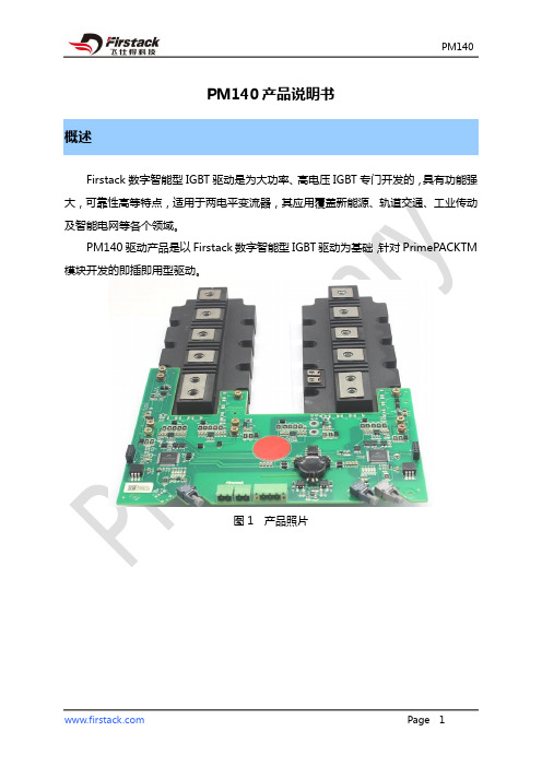
PM140产品说明书概述Firstack数字智能型IGBT驱动是为大功率、高电压IGBT专门开发的,具有功能强大,可靠性高等特点,适用于两电平变流器,其应用覆盖新能源、轨道交通、工业传动及智能电网等各个领域。
PM140驱动产品是以Firstack数字智能型IGBT驱动为基础,针对PrimePACKTM 模块开发的即插即用型驱动。
图1 产品照片目录概述 (1)系统框架图 (3)使用步骤及注意事项 (4)机械尺寸图 (5)引脚定义 (6)状态指示灯说明 (8)驱动参数 (9)主要功能说明 (12)◆短路保护 (12)◆欠压保护 (12)◆软关断 (13)◆温度保护及采样 (13)门极电阻位置指示 (17)订购信息 (19)技术支持 (19)法律免责声明 (19)联系方式 (19)系统框架图数字控制核1D Z1V CC1V EE1软关断电路信号输入1C1级G1级V CC1E1级数字控制核2D Z2V CC2V EE2软关断电路信号输入2C2级G2级V CC2E2级COM1COM2故障指示==V CC1V EE1COM1故障指示电源输入V CE 检测电源检测V CE 检测电源检测故障返回电源V CC2V EE2COM2图2 系统框架图使用步骤及注意事项驱动器简便使用的相关步骤如下:1. 选择合适的驱动器使用驱动器时,应注意该驱动器适配的IGBT模块型号。
对于非指定IGBT 模块无效,使用不当可能会导致驱动和模块失效。
2. 将驱动器安装到IGBT 模块上对IGBT模块或驱动器的任何处理都应遵循国际标准IEC 60747-1第Ⅸ章或欧洲标准EN 100015要求的静电敏感器件保护的一般规范(即工作场所、工具等必须符合这些标准)。
如果忽视这些规范,IGBT和驱动器都可能会损坏。
3. 将驱动器连接到控制单元将驱动器接插件(光纤)连接到控制单元,并为驱动器提供合适的供电电压4. 检查驱动器功能检查门极电压:对于关断状态,额定门极电压在相应的数据手册中给出,对于导通状态,该电压为15V。
全数字IGBT感应加热电源使用说明书(串联型)

目录1. 全数字IGBT感应加热电源(串联型)功能简介 (6)2. 电源结构 (6)3. 使用要求 (6)4. 功能详解 (7)4.1. 实体按钮 (7)4.1.1. 实体按钮概述 (7)4.1.2. 调功电位器 (7)4.1.3. 控制方式切换开关 (7)4.1.4. 断路器操作按钮 (8)4.1.5. 整流单元操作按钮 (8)4.1.6. 逆变单元操作按钮 (8)4.1.7. 急停按钮 (8)4.2. 固定界面 (8)4.3. 主界面 (9)4.3.1. 主界面概述 (9)4.3.2. 主界面左侧电源主要运行数据 (10)4.3.2.1. 当前功率 (10)4.3.2.2. 直流电压 (10)4.3.2.3. 直流电流 (10)4.3.2.4. 逆变电流 (10)4.3.2.5. 炉体电流 (10)4.3.2.6. 当前频率 (10)4.3.2.7. 当前温度 (11)4.3.3. 调功方式切换按钮及功率给定输入框 (11)4.3.4. 数值输入键盘 (11)4.3.5. 控制方式切换按钮 (13)4.3.6. 整流单元操作按钮 (14)4.3.7. 逆变单元操作按钮 (14)4.4. 电能检测 (15)4.4.1. 三相有功功率 (15)4.4.2. 三相视在功率 (15)4.4.3. 三相功率因数 (15)4.4.4. 三相电压 (16)4.4.5. 三相电流 (16)4.4.6. 合相视在功率 (16)4.4.7. 合相视在电能 (16)4.4.8. 合相功率因数 (16)4.4.9. 合相有功功率 (16)4.4.10. 合相有功电能 (16)4.4.11. 电能清零按钮 (16)4.5. 工艺曲线 (17)4.5.1. 工艺曲线 (17)4.5.2. 工艺曲线的设置 (18)4.5.3. 运行工艺曲线 (20)4.6. 实时曲线 (21)4.6.1. 实时曲线 (21)4.6.2. 曲线历史 (22)4.7. 管理 (24)4.7.1. 修改密码 (25)4.7.2. 存储空间 (26)4.7.3. 参数设定 (27)4.7.3.1. 参数设定界面1 (27)4.7.3.2. 参数设定界面2 (29)4.7.3.3. 参数设定界面3 (30)4.7.4. 报警信息 (31)4.7.4.1. 与触摸屏通信中断 (32)4.7.4.2. 直流电压过压报警 (32)4.7.4.3. 直流电压欠压报警 (32)4.7.4.4. 直流电流过流报警 (32)4.7.4.5. 炉体电流过流报警 (33)4.7.4.6. 逆变电流过流报警 (33)4.7.4.7. 加热线圈接地报警 (33)4.7.4.8. SCR水流开关报警 (33)4.7.4.9. IGBT水流开关报警 (33)4.7.4.10. SCR温度开关报警 (34)4.7.4.11. IGBT温度开关报警 (34)4.7.4.12. 开门报警 (34)4.7.4.13. 急停报警 (34)4.7.4.14. 温度反馈断线 (34)4.7.4.15. 直流电压反馈断线 (34)4.7.4.16. 直流电流反馈断线 (34)4.7.4.17. 炉体电流反馈断线 (35)4.7.4.18. 逆变电流反馈断线 (35)4.7.4.19. 频率超上限 (35)4.7.4.20. 频率超下限 (35)4.7.4.21. 电源欠压或缺相 (35)4.7.4.22. 逆变模块X正过流报警 (35)4.7.4.23. 逆变模块X负过流报警 (35)4.7.4.24. IGBT驱动X报警 (35)4.7.4.25. 主板IGBT保护报警 (36)4.7.4.26. 主板正过流保护报警 (36)4.7.4.27. 主板负过流保护报警 (36)4.7.4.28. 主板温度流量保护报警 (36)4.7.5. 报警历史 (36)4.7.6. 状态诊断 (37)5. 通信 (40)6. 安全 (40)7. 电源注册 (41)1.全数字IGBT感应加热电源(串联型)功能简介非常感谢您使用我公司全数字IGBT感应加热电源(以下简称电源),希望我公司的电源能够为您提供更丰富的功能,更高的生产率,更高的效益。
富士IGBT模块应用手册说明书

Quality is our message富士IGBT 模块应用手册富士电机电子设备技术株式会社2004年5月RCH984目录第 1 章构造与特征1. 元件的构造与特征....................................................................................1-22. 富士电机电子设备技术的IGBT...............................................................1-33. 通过控制门极阻断过电流.........................................................................1-54. 限制过电流功能.......................................................................................1-65. 模块的构造..............................................................................................1-66. IGBT模块的电路构造..............................................................................1-7第 2 章术语与特性1. 术语说明..................................................................................................2-22. IGBT模块的特性.....................................................................................2-4第 3 章应用中的注意事项1. IGBT模块的选定.....................................................................................3-22. 静电对策与门极保护................................................................................3-23. 保护电路设计...........................................................................................3-34. 散热设计..................................................................................................3-35. 驱动电路的设计.......................................................................................3-46. 并联连接..................................................................................................3-47. 实际安装的注意事项................................................................................3-58. 保管、搬运上的注意事项.........................................................................3-59. 其他实际使用中的注意事项..................................................................3-5第 4 章发生故障时的应对方法1. 发生故障时的应对方法.............................................................................4-12. 故障的判定方法.......................................................................................4-73. 典型故障及其应对方法.............................................................................4-8第 5 章保护电路设计方法1. 短路(过电流)保护................................................................................5-22. 过电压保护..............................................................................................5-6第 6 章散热设计方法1. 发生损耗的计算方法................................................................................6-22. 散热器(冷却体)的选定方法..................................................................6-73. IGBT模块的安装方法............................................................................6-10第 7 章门极驱动电路设计方法1. 驱动条件和主要特性的关系.....................................................................7-22. 关于驱动电流...........................................................................................7-33. 空载时间的设定.......................................................................................7-54. 驱动电路的具体实例................................................................................7-65. 驱动电路设计、实际安装的注意事项.......................................................7-7第 8 章并联连接1. 电流分配的阻碍原因................................................................................8-22. 并联连接方法...........................................................................................8-3第 9 章评价、测定方法1. 适用范围..................................................................................................9-12. 评价、测定方法.......................................................................................9-1Quality is our message第1章构造与特征目录1. 元件的构造与特征............................................................................................1-22. 富士电机电子设备技术的IGBT.......................................................................1-33. 通过控制门极阻断过电流.................................................................................1-54. 限制过电流功能................................................................................................1-65. 模块的构造.......................................................................................................1-66. IGBT模块的电路构造......................................................................................1-7前言电动机可变速驱动装置和电子计算机的备用电源装置等电力变换器,随着双极型功率晶体管模块和功率MOSFET的出现,已经起了很大的变化。
大功率IGBT智能驱动模块使用手册说明书

WEPOWER2PD632大功率IGBT智能驱动模块使用手册WEPOWER 系列大功率IGBT智能驱动模块是特别为大功率IGBT设计的更为可靠,安全的智能驱动模块。
本产品已获得国家专利授权。
WEPOWER公司推出的系列大功率IGBT智能驱动模块驱动功率大、设计精巧、功能齐全,使用方便,填补了国内在大功率IGBT智能驱动器领域的空白,对我国电力电子技术及相关产业的发展起到了非常积极的促进作用。
我公司生产的2PD632双通道大功率IGBT智能驱动模块可直接替代CONPECT公司的2SD315型产品。
1.主要特点、技术指标和运用1)主要特点:* 适用于大功率IGBT模块驱动* 带短路、过流以及欠压保护* 软关断保护技术* 特别可靠和耐用* 高电气隔离* 开关频率从0~150KHZ* 占空比:0~100%* 抗干扰强,dv/dt>100,000V/us* 内部集成DC/DC电源2)技术指标驱动通道数:2通道;适用母线电压:≤1700V;额定输入电压:15V(±0.5V);最大驱动电流:±32A;内置DC/DC功率:2*6W;PWM输入电平:0-16V(兼容TTL和COMS);额定驱动电压:+15V/-10V;操作温度范围:2PD632I:-40℃~+85℃2PD632J: -40℃~+105℃2PD632M:-55℃~+125℃最大指标符号 定 义 参数 单位 VDD 原边供电电压 16 V VDC 原边供电电压 15.6 V V输入信号电压(高) VS+0.3 V iHV输入信号电压(低) GND-0.3 V iLIout输出峰值电流 16 A PEAK输出平均电流 250 mA IoutAVmax最大开关频率 100 kHz fmax最高C、 E极监测电压 1700 V VCEdv/dt 电压上升率 50 kV/usVisoIIO输入输出隔离电压(AC,RMS,2S) 4000 VVisoIPD 局部放电截止电压,RMS,QPD≤10PC 2000 VVisoI12通道1和通道2隔离电压(AC,RMS,2S)2000 VRGonmin最小开通电阻 0.5 ΩRGoffmin最小关断电阻 0.5 ΩQout/pulse单个脉冲最大输出电能 23 uCTop 使用温度2PD632I -40℃~+85℃℃2PD632J -40℃~+105℃2PD632M -55℃~+125℃Tstg 存储温度2PD632I -55℃~+105℃℃2PD632J -55℃~+125℃2PD632M -60℃~+130℃特性指标符号 定 义参数单位 最小 典型 最大VDD 原边供电电压 14 15 16 V VDC DC/DC供电电压 14.5 15 15.6ISO 原边空载电流 80 mA 原边最大电流 1000 mAVi输入信号电压 15/0 VViT+逻辑高输入门限电压3.5 - - VViT-逻辑低输入门限电压- - 1.5 VVG(on)门极开通电压 +15 VVG(off)门极关断电压 -10 Vtd(on)开通延迟时间 0.2 ustd(off)关断延迟时间 0.22 ustd(err)故障输出延迟时间 0.5 ustTD 通道1和通道2内部默认死区时间1.8 usCPS原副边耦合电容 17 pF VCEsat VEC过流保护门限 9 V W 重量 35 gMTBF 平均无故障时间(Ta=40℃,最大负载)1.6 106h3)应用z逆变器z电机驱动z机车牵引z大功率变换器z大型开关电源2、2PD632外形尺寸及引脚排列引脚功能引脚功能1 VDD +15V 输入端电源2 VDD +15V输入端电源3 SO1 通道A故障输出4 /RST 复位输入5 CA 通道A死区电容6 inB B通道输入7 CB 通道B死区电容8 NC9 SO2 通道B故障输出10 inA A通道输入11 GND 输入端电源地12 GND 输入端电源地13 VDC 内部DC/DC +15V 输入14 VDC 内部DC/DC +15V 输入15 VDC 内部DC/DC +15V 输入16 VDC 内部DC/DC +15V 输入17 VDC 内部DC/DC +15V 输入18 GND(dc) 内部DC/DC电源地19 GND(dc) 内部DC/DC电源地20 GND(dc) 内部DC/DC电源地21 GND(dc) 内部DC/DC电源地22 GND(dc) 内部DC/DC电源地44 G1 通道1门极输出43 G1 通道1门极输出42 COM1 通道1公共端41 COM1 通道1公共端40 NC39 E1 通道1E极38 E1 通道1E极37 NC36 C1 通道1C极检测端35 NC34 NC33 NC32 G2 通道2门极输出31 G2 通道2门极输出30 COM2 通道2公共端29 COM2 通道2公共端28 NC27 E2 通道2E极26 E2 通道2E极25 NC24 C2 通道2C极检测端23 NC3.应用举例下图是2PD632的运用参考电路。
- 1、下载文档前请自行甄别文档内容的完整性,平台不提供额外的编辑、内容补充、找答案等附加服务。
- 2、"仅部分预览"的文档,不可在线预览部分如存在完整性等问题,可反馈申请退款(可完整预览的文档不适用该条件!)。
- 3、如文档侵犯您的权益,请联系客服反馈,我们会尽快为您处理(人工客服工作时间:9:00-18:30)。
1MBH15-120,1MBH15D-120,Molded IGBT1200V / 15AMolded PackageFeatures· Small molded package · Low power loss· Soft switching with low switching surge and noise· High reliability, high ruggedness (RBSOA, SCSOA etc.)· Comprehensive line-upApplications· Inverter for Motor drive· AC and DC Servo drive amplifier· Uninterruptible power supplyMaximum ratings and characteristicsAbsolute maximum ratings (at Tc=25°C unless otherwise specified)Item Symbol Collector-Emitter voltage V CES Gate-Emitter voltaga V GES Collector DC Tc=25°C I C25current Tc=100°C I C1001ms Tc=25°C IcpMax. power dissipation(IGBT)P C Operating temperature T j Storage temperature T stg Screw torque - Rating1200±2026 1578245+150-40 to +150 70Unit V V A A A W °C °C N·mEquivalent Circuit Schematic1MBH15-120 / IGBT1MBH15D-120 / IGBT+FWDIGBTIGBT + FWDItemZero gate voltage collector current Gate-Emitter leakage current Gate-Emitter threshold voltage Collector-Emitter saturation voltage Input capacitance Output capacitanceReverse transfer capacitance Turn-on time Turn-off timeI CES I GES V GE(th)V CE(sat)C ies Coes C res t on t r t off t f–– 1.0––205.5–8.5–– 3.5–1700––300––120––– 1.2––0.6–– 1.5––0.5V GE =0V, V CE =1200V V CE =0V, V GE =±20V V CE =20V, I C =15mA V GE =15V, I C =15A V GE =0V V CE =10V f=1MHzV CC =600V I C =15A V GE =±15V R G =120 ohm (Half Bridge)mA µA V V pFµsElectrical characteristics (at Tj=25°C unless otherwise specified)Thermal resistance characteristics Symbol Characteristics Conditions Unit Min. Typ. Max.1MBH15-120 / IGBT1MBH15D-120 / IGBT+FWDThermal resistance ––0.51IGBT °C/W Item Symbol Characteristics Conditions Unit Min. Typ. Max.Rth(j-c)1MBH15-120 / IGBTOutline drawings, mm1MBH15-120, 1MBH15D-120TO-3PLCharacteristics1MBH15-120,1MBH15D-120Collector current vs. Collector-Emitter voltage Tj=25°CCollector current vs. Collector-Emitter voltage Tj=125°CCollector-Emitter vs. Gate-Emitter voltage Tj=25°CCollector-Emitter vs. Gate-Emitter voltage Tj=125°CSwitching time vs. Collector currentVcc=600V, R G =120 ohm, V GE =±15V, Tj=25°C Switching time vs. Collector currentVcc=600V, R G =120 ohm, V GE =±15V, Tj=125°CCollector-Emitter voltage : V CE [V]Collector-Emitter voltage : V CE [V]C o l l e c t o r c u r r e n t : I c [A ]C o l l e c t o r c u r r e n t : I c [A ]0 1 2 3 4 5C o l l e c t o r -E m i t t e r v o l t a ge:V C E [V ]C o l l e c t o r -E m i t t e r v o l t a g e : V C E [V ]0 5 10 15 20Gate-Emitter voltage : V GE [V]Gate-Emitter voltage : V GE [V]S w i t c h i n g t i m e : t o n , t r , t o f f , t f [n s e c .]100Collector current : Ic [A]Collector current : Ic [A]S w i t c h i n g t i m e : t o n , t r , t o f f , t f [n s e c .]0 5 10 15 20 25504030201010864210001086 4 2 010010000 1 2 3 4 50 5 10 15 20Collector-Emitter voltage : V CE [V]10C a p a c i t a n c e : C i e s , C o e s , C r e s [n F ]Capacitance vs. Collector-Emitter voltageTj=25°C0 5 10 15 20 25 30 35100Switching time vs. R GVcc=600V, Ic=15A, V GE =±15V, Tj=25°C Dynamic input characteristicsTj=25°CGate resistance : R G [ohm]Gate charge : Qg [nC]1001000S w i t c h i n g t i m e : t o n , t r , t o f f , t f [n s e c .]C o l l e c t o r -E m i t t e r v o l t a g e : V C E [V ]G a t e -E m i t t e r v o l t a g e : V G E [V ]353025201510500 200 400 600 800 1000 1200Collector-Emitter voltage : V CE [V]C o l l e c t o r c u r r e n t : I c [A ]0 50 100 150 2002520151051000800600400200Switching time vs. R GVcc=600V, Ic=15A, V GE =±15V, Tj=125°CGate resistance : R G [ohm]1001000100S w i t c h i n g t i m e : t o n , t r , t o f f , t f [n s e c .]Reversed biased safe operating area+V GE =15V, -V GE = 15V, Tj = 125°C, R G = 120 ohm<<>Typical short circuit capabilityVcc=800V, R G =120 ohm, Tj=125°CS h o r t c i r c u i t t i m e : t s c [µs ]100050040030020010005 10 15 20 255040302010S h o r t c i r c u i t t i m e c u r r e n t : I s c [A ]Characteristics1MBH15-120,1MBH15D-120Gate voltage : V GE [V]10010-4 10-3 10-2 10-1 100Pulse width : P W [sec.]T h e r m a l r e s i s t a n c e : R t h (j -c ) [°C /W ]Transient thermal resistanceCharacteristics1MBH15-120,1MBH15D-1201MBH15D-120Reverse recovery time vs. Forward current-di/dt=45A / µsecReverse recovery current vs. Forward current -di/dt=45A / µsecr e v e r s e r e c o v e r y t i m e : t r r [n s e c ]r e v e r s e r e c o v e r y c u r r e n t : I r r [A ]8006004002001086420 5 10 15 20 25 30Forward current : I F [A]Forward current : I F [A]0 1.0 2.0 3.0 4.00 50 100 150 200Forward voltage : V F [V]F o r w a r d c u r r e n t : I F [A ]r e v e r s e r e c o v e r y t i m e : t r r [n s e c ]-di/dt [ A / µsec ]Forward current vs. Foeward voltageReverse recovery time characteristics vs. -di/dt IF=15A , Tj=125°C2015105r e v e r s e r e c o v e r y c u r r e n t : I r r [A ]10010-110-21015040302010800600400200 0。