SS2C中文资料
SS1040中文资料

SS1040SURFACE MOUNT SCHOTTKY BARRIER DIODECharacteristicSymbol SS1040UnitPeak Repetitive Reverse Voltage Working Peak Reverse Voltage DC Blocking Voltage V RRM V RWM V R 40V Forward Continuous Current (Note 1)I F1.0ANon-Repetitive Peak Forward Surge Current 8.3ms Single half sine-wave superimposed on rated load (JEDEC Method)I FSM 25A Power Dissipation (Note 1)P d 450mW Typical Thermal Resistance, Junction to Ambient Air (Note 1)R JA 222°C/W Operating and Storage Temperature RangeT j , T STG-65 to +125°CElectrical Characteristics @T A =25°C unless otherwise specifiedCharacteristicSymbol SS1040Unit Forward Voltage Drop @I F = 1.0A V FM 0.55V Peak Reverse Leakage Current @ DC Blocking Voltage I RM 500µA Typical Junction Capacitance (V R = 4V DC, f = 1MHz)C j50pFNote: 1. Valid provided that terminals are kept at ambient temperature.WTEI ,A V E R A G E O U T P U T C U R R E N T (A )O 00.20.40.60.81.010406080100120140T , TERMINAL TEMPERATURE (ºC)T Fig. 1 Forward Current Derating Curve0.010.11100.0010.00011.00.60.80.40.2I ,I N S T A N T A N E O U S F O R W A R D C U R R E N T (A )F V ,INSTANTANEOUS FORWARD VOLTAGE (V)F Fig.2Typical Forward CharacteristicsC ,T O T A L C A P A C I T AN C E (p F )T V , REVERSE VOLTAGE (V)R Fig. 4Typical Total Capacitance10001010010203040510152025110100I ,P E A K F O R W A R D S U R G E C U R R E N T (A )F S M NUMBER OF CYCLES AT 60 HzFig.3 Maximum Non-Repetitive Peak Fwd Surge CurrentMARKING INFORMATION RECOMMENDED FOOTPRINTPACKAGING INFORMATIONORDERING INFORMATIONProduct No.Package TypeShipping QuantitySS1040-T1SOD-1233000/Tape & Reel1. Shipping quantity given is for minimum packing quantity only. For minimumorder quantity, please consult the Sales Department.2.To order RoHS / Lead Free version (with Lead Free finish), add “-LF” suffix to part number above. For example, SS1040-T1-LF .Won-Top Electronics Co., Ltd (WTE) has checked all information carefully and believes it to be correct and accurate. However, WTE cannot assume any responsibility for inaccuracies. Furthermore, this information does not give the purchaser of semiconductor devices any license under patent rights to manufacturer. WTE reserves the right to change any or all information herein without further notice.WARNING : DO NOT USE IN LIFE SUPPORT EQUIPMENT. WTE power semiconductor products are not authorized for use as critical components in life support devices or systems without the express written approval.We power your everyday.Won-Top Electronics Co., Ltd.No. 44 Yu Kang North 3rd Road, Chine Chen Dist., Kaohsiung, Taiwan Phone: 886-7-822-5408 or 886-7-822-5410Fax: 886-7-822-5417Email: sales@Internet: 。
SS24中文资料_数据手册_参数

Symbol
Parameter
Value Units
SS22 SS23 SS24 SS25 SS26 SS28 SS29 S210
VRRM
Maximum Repetitive Reverse Voltage
20 30 40 50 60 80 90 100 V
IF(AV)
Maximum Average Forward Current: 0.375-inch Lead Length at TA = 75°C
2.0
A
Non-Repetitive Peak Forward Surge
IFSM Current: 8.3 ms Single Half-Sine
50
A
Wave Temperature Range Operating Junction Temperature
-65 to +150
October 2013
Description
The SS22-S210 series includes high-efficiency, low power loss, general-propose Schottky rectifiers. The clipbonded leg structure provides high thermal performance and low electrical resistance. These rectifier are suited for free wheeling, secondary rectification, and reverse polarity protection applications.
Value
SS22 SS23 SS24 SS25 SS26 SS28 SS29 S210
MIL-STD-1275B中文资料

SENSITRONSEMICONDUCTORSPDXXD28 SERIES TECHNICAL DATADATASHEET 4310, Rev BDC Solid State Power Controller ModuleDescription:The Solid State Power Controller (SSPC) Module is a microcontroller-based Solid State Relay rated upto 25A designed to be used in Army, Air force and Navy in 28V DC applications. This module has integrated current sensing with no derating over the full operating temperature range. The module is the electronic equivalent to an electromechanical circuit breaker with isolated control and status.This series is supplied in 3 product families covering 9 current ranges:SPD5D28 Family:1A- SPD5D28-1:- SPD5D28-3:3A5A- SPD5D28-5:SPD15D28 Family:7A- SPD14D28-7:- SPD14D28-10:10A14A- SPD14D28-14:SPD25D28 Family:15A- SPD25D28-15:20A- SPD25D28-20:25A- SPD25D28-25:Compliant Documents & Standards:MIL-STD-1275B, Notice1 Characteristics of 28 Volt DC Electrical Systems in Military Vehicles-4/20/04Power Characteristics 12 March 2004 MIL-STD-704F AircraftElectricalMIL-STD-217F, Notice 2 Reliability Prediction of Electronic Equipment 28 Feb 1995Module Features:•Epoxy Shell Construction Array•Solid State Reliability; Low Weight (20 gms) - High Power Density•Same Pin Out as Industry Standard SSPCs in a Smaller Outline•Extremely Low Power, No Derating Over the Full Temperature RangeElectrical Features (SPDXXD28 Series):•28VDC Input with Very Low Voltage Drop; 60mV, typ. @15A• True I2t Protection from 32A to 250A with Nuisance Trip Suppression•Instant Trip Protection (50 µsec typ) for Loads Above 250A•Unlimited Interrupt Capability; Repetitive Fault Handling Capability• Thermal Memory•Internally Generated Isolated Supply to Drive the Switch•Low Bias Supply Current: 20 mA typ @ 5V DC•High Control Circuit Isolation: 750V DC Control to Power Circuit•Soft Turn-On to Reduce EMC Issues• EMI Tolerant•Module Reset with a Low Level Signal; Reset Circuit is Trip-Free•TTL/CMOS Compatible, Optically Isolated, Input and OutputsSENSITRONSEMICONDUCTORTECHNICAL DATADATASHEET 4310, Rev B SPDXXD28 SERIESTable 1 - Electrical Characteristics (at 25 o C and V bias = 5.0V DC unless otherwise specified)PowerInput Voltage – Continuous – Transient 0 to 40V DC, 50V DC Absolute Maximum +600V or –600V Spike (< 10 uS) Power Dissipation See Table 4 CurrentSee Table 4 See Trip Curve Max Voltage DropSee Table 4 Max current without tripping110% minTrip timeSee Trip Curve Output Rise Time (turn ON)110 µsec typ Output Fall Time under normal turn-off 110 usec typ Output Fall Time under Fault 50 usec typ Min Load RequirementNilProtectionShort Circuit Protection UnlimitedInstant Trip800%, min; 1200%, maxPhysical CharacteristicsTemperatureOperating Temperature T A = -55 °C to +100 °C Storage TemperatureT A = -55 °C to +125 °CEnvironmentalAltitudeUp to 30,000 ftCan be installed in an unpressurized area Case Dimensions 1.825”L x 1.25”W x 0.38”H Operating Orientation AnyWeight20 grams typMTBF (Estimate: MIL STD 217F)1.1 Mhrs at 25°C Full loadControl & Status (TTL/CMOS Compatible)BIAS (Vcc)5.0V DC Nominal,6.5V DC Absolute Maximum 4.5V to 5.5 VDC BIAS (Vcc) Current20 mA typ 25 mA, maxGATE Status, Load Status SignalsV oh =3.7V, min, at I oh =-20mA V ol =0.4V, max, at I ol =20mA CONTROL SignalV T+ (Positive-going input threshold voltage) V T − (Negative-going input threshold voltage) ∆V T Hysteresis (V T + V T −)2.0V, min,3.5V, max 1.2V, min, 2.3V, max 0.6V, min, 1.4V, maxResetCycle CONTROL SignalSENSITRONSEMICONDUCTORTECHNICAL DATADATASHEET 4310, Rev BSPDXXD28 SERIESFigure 1 - Trip CurveFigure 2 - Timing DiagramSENSITRONSEMICONDUCTORTECHNICAL DATADATASHEET 4310, Rev BSPDXXD28 SERIESTable 2 - Signal Timing – (-55 o C to 100 o C @ LINE = 28V DC)Parameter Symbol Min MaxUnitsCONTROL to GATE Status Delay for Turn On t0 1 ms Turn ON Delay t1 200 µs Load Current Rise Time t2 50 200 µs Turn ON to LOAD Status Delay t3 1 ms CONTROL to GATE Status Delay for Turn Off t4 1 ms Turn OFF Delay t5 200 µs Load Current Fall Time t6 50 200 µs Turn OFF to LOAD Delay t7 1 ms Note: Current Fall Time from trip dependent on magnitude of overloadFigure 3 - Mechanical DimensionsTable 3 - Pin DefinitionsPin Number Pin NameFunction1 BIAS+5V DC Supply 2 GND 5V Return 3 GATE Status Switch Status4 LOAD Status Load Current Detection5 CONTROL Input On/Off Control6 LINE+28V DC Supply 7 ---No Pin 8 PWRGND 28V ReturnSENSITRONSEMICONDUCTORTECHNICAL DATADATASHEET 4310, Rev BSPDXXD28 SERIESTable 4 – Individual Model RatingsSPD5D28 FamilyModel SPD5D28-1 SPD5D28-3 SPD5D28-5 Current Rating @ 100O C1A 3A 5APower Dissipation 0.01W typ @ 0.6A 25O C0.035W max @ 1A 25O C0.04W max @ 1A 100O C0.04W typ @ 1.8A 25O C0.14W max @ 3A 25O C0.16W max @ 3A 100O C0.09W typ @ 3A 25O C0.30W max @ 5A 25O C0.36W max @ 5A 100O CMax Voltage Drop 18mV typ @ 0.6A 25O C35mV max @ 1A 25O C40mV max @ 1A 100O C23mV typ @ 1.8A 25O C46mV max @ 3A 25O C53mV max @ 3A 100O C30mV typ @ 3A 25O C60mV max @ 5A 25O C71mV max @ 5A 100O CSPD14D28 FamilyModel SPD14D28-7 SPD14D28-10 SPD14D28-14 Current Rating @ 100O C7A 10A 14APower Dissipation 0.15W typ @ 4.2A 25O C0.49W max @ 7A 25O C0.60W max @ 7A 100O C0.26W typ @ 6A 25O C0.87W max @ 10A 25O C1.10W max @ 10A 100O C0.48W typ @ 8.4A 25O C1.61W max @ 14A 25O C2.06W max @ 14A 100O CMax Voltage Drop 35mV typ @ 4.2A 25O C70mV max @ 7A 25O C86mV max @ 7A 100O C43mV typ @ 6A 25O C87mV max @ 10A 25O C110mV max @ 10A 100O C57mV typ @ 8.4A 25O C115mV max @ 14A 25O C147mV max @ 14A 100O CSPD25D28 FamilyModel SPD25D28-16 SPD25D28-20 SPD25D28-25 Current Rating @ 100O C16A 20A 25APower Dissipation 0.41W typ @ 9.6A 25O C1.44W max @ 16A 25O C1.73W max @ 16A 100O C0.60W typ @ 12A 25O C2.11W max @ 20A 25O C2.56W max @ 20A 100O C0.90W typ @ 15A 25O C3.15W max @ 25A 25O C3.86W max @ 25A 100O CMax Voltage Drop 43mV typ @ 9.6A 25O C90mV max @ 16A 25O C108mV max @ 16A 100O C50mV typ @ 12A 25O C105mV max @ 20A 25O C128mV max @ 20A 100O C60mV typ @ 15A 25O C126mV max @ 25A 25O C154mV max @ 25A 100O CSENSITRONSEMICONDUCTORSPDXXD28 SERIES TECHNICAL DATADATASHEET 4310, Rev BFigure 4 - Electrical Block DiagramDescriptionFigure 4 shows the block diagram of the SPDXXD28 SSPC Series. It uses a SN74LVC3G14 device for digital I/O. This TTL compatible device has a Schmitt-Trigger input to minimize the effects of noise on the input. Its outputs can each drive more than 10 standard TTL loads. It’s also compatible with CMOS inputs and outputs. The SN74LVC3G14 is isolated from the remainder of the module circuitry by three optocouplers.The block labeled “Control & Protection Circuitry” gets power from the DC-DC converter and is referenced to the output of the SSPC. This block contains an amplifier to gain up the voltage developed across the sense resistor. It also contains a microcontroller with on-board timers, A/D converter, clock generator and independent watchdog timer. The microcontroller implements a precision I2t protection curve as well as an Instant Trip function to protect the wiring and to protect itself. It performs all of the functions of multiple analog comparators and discrete logic in one high-reliability component.The code programmed in the microcontroller acquires the output of the internal A/D converter, squares the result and applies it to a simulated RC circuit. It checks the output of the simulated circuit to determine whether or not to trip (turn off the power Mosfets). Because the microcontroller simulates an analog RC circuit, the SSPC has ‘thermal memory’. That is, it trips faster if there had been current flowing prior to the overload than if there hadn’t been current flowing. This behavior imitates thermal circuit breakers and better protects the application’s wiring since the wiring cannot take as much an overload if current had been flowing prior to the overload.SENSITRONSEMICONDUCTORSPDXXD28 SERIES TECHNICAL DATADATASHEET 4310, Rev BThe watchdog timer operates from its own internal clock so a failure of the main clock will not stop the watchdog timer. The code programmed in the microcontroller will periodically reset the watchdog timer preventing it from timing out. If the code malfunctions for any reason, the watchdog timer is not reset and it times out. When the watchdog timer times out, it resets the microcontroller. Since the code is designed to detect levels and not edges, the output of the module, and therefore the output of the SPDXXD28, immediately reflects the command on its input.The Power Mosfets used in the SPDXXD28 Series have been selected for very low R ds(on) and results in low voltage drop and low power dissipation. In most applications, the SPDXXD28 will be operated at 50 – 60% of rated current to provide a safety margin. As can be seen in Table 1, when the SPD25D28 is operated at 15 Amps, 60% of rated current, it only dissipates 1.0 Watt at room temperature. No heatsinking is required for this condition. However, if the SPD25D28 is to be operated at maximum rating and/or at elevated temperatures, the dissipation can exceed 4 Watts and heatsinking is required. Some heatsinking can be accomplished by adding copper area to the LINE and LOAD pins, a heatsink can be epoxied to the surface of the module or a flat copper or aluminum heatsink can be sandwiched between the SPD25D28 and the printed circuit board using a thermal pad to maximize heat transfer. Each application should be evaluated at maximum expected constant current. For overloads, no heatsinking is required provided the SPDXXD28 Series is allowed some time to cool down. The SPDXXD28 has sufficient thermal mass that the temperature will rise only a few degrees under the worst-case overload. Repetitive overloads should be avoided. When the SPDXXD28 reports a trip condition, the controller driving the SPDXXD28 should allow no more than four repetitions and then allow thirty seconds to cool down before trying to turn on again.The SPDXXD28 will trip on overloads in the ALWAYS TRIP region shown in Figure 1 and will never trip when in the NEVER TRIP region. The SPDXXD28 can be reset by bringing the CONTROL pin to a logic low. When the CONTROL pin is brought back to logic high, the SPDXXD28 will turn back on. If the overload is still present, the SPDXXD28 will trip again. Cycling the 5 Volt BIAS power will also reset the SPDXXD28. If the CONTROL pin is at logic high when the BIAS power is cycled, the SPDXXD28 will turn back on when the BIAS power is re-applied.Status OutputsThe LOAD and GATE status outputs of the SPDXXD28 show whether or not the load is drawing current and whether or not the SPDXXD28 Power Mosfet switch is on. A logic high on the LOAD status output shows that the load draws < 5% of rated load and a logic low shows that the load draws > 15% of rated current. A load that draws between 5% and 15% of rated current could result in either a high or low logic level on the LOAD status output. A logic high on the GATE output indicates that the Power Mosfet switch is on while a logic low indicates that the switch is off.As can be seen in Table 4, of the 8 possible states for the combination of CONTROL, LOAD and GATE, only 3 states represent valid SSPC operation. The other 5 states indicate either a failed SSPC or, more likely, a short to ground or a short to the BIAS supply of one of the logic outputs. By comparing the CONTROL input with the LOAD and GATE outputs, the user can determine whether or not the load is supposed to be ON (GATE), whether or not it’s drawing current (GATE) and whether or not the LOAD and GATE outputs are valid responses to the CONTROL input.Table 4 – CONTROL, LOAD & GATE Truth TableState CONTROL LOAD GATE Comments1 L L L SSPC failure or shorted LOAD output to groundfailure2 L L H SSPCOFFcondition3 L H L Normal4 L H H SSPC failure or shorted GATE output to BIAS supply5 H L L SSPC failure or shorted GATE output to ground6 H L H Normal ON condition with load current > 15% rated currentSENSITRONSEMICONDUCTORTECHNICAL DATADATASHEET 4310, Rev BSPDXXD28 SERIESWire SizeMIL-W-5088L has a chart the shows wire size as a function of wire temperature and current. This chart is for a single copper wire in free air. For an ambient temperature of 70 o C, the chart allows an 18-gauge wire to handle 25 Amps continuously at a wire temperature of 200 o C – a wire temperature rise of 130 o C. For a wire temperature limited to 150 o C, the chart requires a 16-gauge wire and for a wire temperature of 105 o C, the chart requires a 14-gauge wire.Amendment 1 of MIL-W-5088L has a table for copper wire in a bundle, group or harness with conditions on the number of wires, percent of total harness capacity, etc. This table shows that a 12 gauge wire is necessary for 200 o C operation, 10 gauge for 150 o C and 8 gauge for 105 o C.MIL-W-5088L has various figures showing derating for harnesses as a function of the number of current carrying conductors and for altitude. MIL-W-5088L only specifies wire for DC or RMS AC conditions, not for transient or overload conditions.For transient or overload conditions, the transient or overload happens so quickly that heat is not transferred from the wire to the surroundings. The heat caused by the I 2R heating of the wire causes the temperature to rise at a linear rate controlled by the heat capacity of the wire. The equation for this linear rise in temperature, with respect to time, can be solved as: I 2t = constant. Every wire has an I 2t rating that’s dependent on the temperature rise allowed and the diameter of the wire. If the I 2t rating of the SSPC or circuit breaker is less than the I 2t rating of the wire, then the SSPC or circuit breaker can protect the wire. The maximum I 2t rating for the SPD25D28 is 7.45 Amp 2-Seconds. Every wire size in the paragraphs above has an I 2t rating that exceeds the SPD25D28 I 2t rating for the temperature rises stated. Therefore, to select a wire size, it’s simply a matter of determining the maximum temperature rise of the application and deciding whether or not the wire will be in a bundle and use the information above.Application ConnectionsThe SPDXXD28 Series may be configured as a high-side or low-side switch and may be used in positive ornegative supply applications. Figure 5 shows the connections as a high-side switch with a positive power supply.SENSITRONSEMICONDUCTORTECHNICAL DATADATASHEET 4310, Rev BSPDXXD28 SERIESFigure 6 shows a low-side switch with a negative power supply. Note that the PWRGND pin is now connected to the LINE pin (see Rise/Fall Time paragraph below for more information on the PWRGND pin).Figure 6 – Low-Side Switch, Positive SupplyFigures 7 and Figure 8 show negative supply high-side switch and low-side switch implementations. Again, note the connection of the PWRGND pin.SENSITRONSEMICONDUCTORSPDXXD28 SERIES TECHNICAL DATADATASHEET 4310, Rev BFigure 8 – Low Side Switch, Negative SupplyRise Time & Fall TimeThe rise and fall times of the SPDXXD28 is pre-set at the factory for a nominal 100uS with a LINE supply of 28VDC (see Table 2 for min/max limits). The rise and fall times will vary linearly with supply voltage. The PWRGND pin is used to control the rise and fall times. If the PWRGND pin is left open, the rise and fall times will be about 50uS. Leaving the PWRGND pin open can be useful when a faster rise or fall time is desirable. With the PWRGND pin connected as in Figures 5 through 8, the SPDXXD28 can turn on into a capacitive load of 440uF, min, 880uF, typ, without tripping for any power supply voltage within the ratings.Wiring and Load InductanceWiring inductance can cause voltage transients when the SPDXXD28 is switched off due to an overload. Generally, these transients are small but must be considered when long wires are used on either the LINE or LOAD pins or both. A 10 foot length of wire in free air will cause a transient voltage of about 10 Volts when the SPD25D28 trips at an Instant Trip level of 250 Amps. At the rated load current of 25 Amps, the voltage transient will be about 1 Volt. If longer wire lengths are used, a transient suppressor may be used at the LINE pin and a power diode may be used at the LOAD pin so that the total voltage between the LINE and LOAD pins is less than 50 Volts.When powering inductive loads, the negative voltage transient at the LOAD pin can cause the voltage between LINE and LOAD to exceed the SPDXXD28 rating of 50 Volts and a power diode from the LOAD pin to ground must be used. The cathode of the power diode is connected to the LOAD pin with the anode connected to ground. The power diode must be able to carry the load current when the SPDXXD28 switches off.ParallelingFor example, putting two SPD25D28s in parallel will not double the rating to 50 Amps. Due to differences in the R ds(on) of the Power Mosfets in the SSPCs, the current will not share equally. In addition, there are unit-to-unit differences in the trip curves so that two SPD25D28s in parallel may possibly trip at 35 Amps. Also, bothSENSITRONSEMICONDUCTORTECHNICAL DATADATASHEET 4310, Rev B• 221 West Industry Court Deer Park, NY 11729-4681 Phone (631) 586 7600 Fax (631) 242 9798 •• World Wide Web - • E-Mail Address - sales@ • SPDXXD28 SERIESBoard LayoutThe current-carrying power circuit should be kept well away from the control circuit and other low-level circuits in the system. It’s unlikely, but possible, that magnetic coupling could affect the control circuit when turning normal loads on and off. However, in the case of an overload, the magnetic coupling could be 10 times greater than with normal loads. Effects of such coupling could cause ‘chattering’ when turning on and off, oscillation, and the possibility of turning the SPDXXD28 back on after an overload. The SPDXXD28 Series is a Trip-Free device. Once tripped it will not turn back on until reset and commanded on again. Reset is accomplished by bringing the CONTROL pin low and turning the SSPC back on is accomplished by bringing the CONTROL pin high. Sufficient magnetic coupling between the current-carrying power circuit and the control circuit can negate the Trip-Free characteristic.MIL-STD-704F and MIL-STD-1275BThese standards cover the characteristics of the electrical systems in Military Aircraft and Vehicles. The SPDXXD28 Series meets all of the requirements of MIL-STD-704F including Normal, Emergency, Abnormal and Electric Starting conditions with the Ripple, Distortion Factor and Distortion Spectrum defined in the standard. The SPDXXD28 Series also meets all of the requirements of MIL-STD-1275B including operation with Battery and Generator, Generator Only and Battery Only for all of the conditions described in the standard including Cranking, Surges, Spikes and Ripple.In addition, the SPDXXD28 Series can withstand + 600 V spikes for 10uS. This capability is beyond that required by the standards cited above.DISCLAIMER:1- The information given herein, including the specifications and dimensions, is subject to change without prior notice to improve product characteristics. Before ordering, purchasers are advised to contact the Sensitron Semiconductor sales department for the latest version of the datasheet(s).2- In cases where extremely high reliability is required (such as use in nuclear power control, aerospace and aviation, traffic equipment, medical equipment , and safety equipment) , safety should be ensured by using semiconductor devices that feature assured safety or by means of users’ fail-safe precautions or other arrangement .3- In no event shall Sensitron Semiconductor be liable for any damages that may result from an accident or any other cause during operation of the user’s units according to the datasheet(s). Sensitron Semiconductor assumes no responsibility for any intellectual property claims or any other problems that may result from applications of information, products or circuits described in the datasheets.4- In no event shall Sensitron Semiconductor be liable for any failure in a semiconductor device or any secondary damage resulting from use at a value exceeding the absolute maximum rating.5- No license is granted by the datasheet(s) under any patents or other rights of any third party or Sensitron Semiconductor.6- The datasheet(s) may not be reproduced or duplicated, in any form, in whole or part, without the expressed written permission of Sensitron Semiconductor.7- The products (technologies) described in the datasheet(s) are not to be provided to any party whose purpose in their application will hinder maintenance of international peace and safety nor are they to be applied to that purpose by their direct purchasers or any third party. When exporting these products (technologies), the necessary procedures are to be taken in accordance with related laws and regulations.元器件交易网。
W25Q64中文资料精编版
W25Q64BV出版日期:2010年7月8日- 1 - 版本E64M位与串行闪存双路和四路SPIW25Q64BV- 2 -目录1,一般DESCRIPTION (5)2。
FEATURES (5)3引脚配置SOIC208-MIL.......................................... .. (6)4,焊垫配置WSON8X6-MM.......................................... . (6)5,焊垫配置PDIP300-MIL.......................................... . (7)6引脚说明SOIC208密耳,PDIP300密耳和WSON8X6-MM................................ 7......7引脚配置SOIC300mil的.......................................... .. (8)8引脚SOIC封装说明300-MIL (8)8.1包装Types (9)8.2片选(/CS) (9)8.3串行数据输入,输出和IO(DI,DO和IO0,IO1,IO2,IO3)............................. 9.......8.4写保护(/WP) (9)8.5控股(/HOLD) (9)8.6串行时钟(CLK) (9)9座DIAGRAM (10)10功能DESCRIPTION (11)10.1 SPI OPERATIONS (11)10.1.1标准SPI Instructions (11)10.1.2双SPI Instructions (11)10.1.3四路SPI Instructions (11)10.1.4保持功能 (11)10.2写保护 (12)10.2.1写保护Features (12)11,控制和状态寄存器............................................ .. (13)11.1状态REGISTER (13)11.1.1 BUSY (13)11.1.2写使能锁存(WEL) (13)11.1.3块保护位(BP2,BP1,BP0)..................................... .. (13)11.1.4顶/底块保护(TB)....................................... .................................................. ..1311.1.5部门/块保护(SEC) (13)11.1.6状态寄存器保护(SRP,SRP0)....................................... . (14)11.1.7四路启用(QE) (14)11.1.8状态寄存器内存保护........................................... .. (16)11.2 INSTRUCTIONS (17)11.2.1制造商和设备标识........................................... .. (17)11.2.2指令集表1 (18)W25Q64BV11.2.3指令表2(阅读说明书)....................................... (19)出版日期:2010年7月8日- 3 - 修订版E11.2.4写使能(06h) (20)11.2.5写禁止(04h) (20)11.2.6读状态寄存器1(05H)和读状态寄存器2(35H).............................. (21)11.2.7写状态寄存器(01H)......................................... .................................................. .. (22)11.2.8读取数据(03h) (23)11.2.9快速阅读(0Bh) (24)11.2.10快速读双输出(3BH)........................................ .................................................. 0.25 11.2.11快速读四路输出(6BH)........................................ .. (26)11.2.12快速读双I / O (BBh) (27)11.2.13快速读取四I/ O (EBh) (29)11.2.14八进制字读取四I/ O(E3H)..................................... (31)11.2.15页编程(02h) (33)11.2.16四路输入页编程(32H)........................................ . (34)11.2.17扇区擦除(20H) (35)11.2.1832KB的块擦除(52H) (36)11.2.1964KB的块擦除(D8h) (37)20年2月11日芯片擦除(C7H/ 60h) (38)21年2月11日擦除挂起(75h) (39)22年2月11日擦除恢复(7Ah) (40)23年11月2日掉电(B9h) (41)24年2月11日高性能模式(A3H)......................................... (42)25年2月11日发布掉电或高性能模式/设备ID(ABH) (42)26年2月11日读制造商/设备ID(90H)....................................... . (44)27年2月11日阅读唯一的ID号(4BH)........................................ . (45)28年2月11日读JEDEC的ID (9Fh) (46)29年2月11日连续读取模式复位(FFH或FFFFH)...................................... .. (47)12,电气特性.............................................. (48)12.1绝对最大Ratings (48)12.2操作范围 (48)12.3上电时序和写抑制阈值......................................... (49)12.4直流电气Characteristics (50)12.5 AC测量条件.............................................. .. (51)12.6 AC电气Characteristics (52)12.7 AC电气特性(续)......................................... . (53)12.8串行输出Timing (54)12.9输入Timing (54)12.10持有Timing (54)13包装SPECIFICATION (55)W25Q64BV13.18引脚SOIC208密耳(包装代号SS)..................................... .. (55)- 4 -13.28引脚PDIP300密耳(封装代码DA)..................................... (56)13.38触点WSON8x6毫米(封装代码ZE)....................................... (57)13.416引脚SOIC300密耳(封装代码SF)..................................... . (58)14订货INFORMA TION (59)14.1有效的部件号和顶端标记.......................................... (60)15版本HISTORY (61)W25Q64BV出版日期:2010年7月8日- 5 - 修订版E1概述该W25Q64BV(64M位)串行Flash存储器提供了有限的系统存储解决方案空间,引脚和电源。
4066中文资料
Sine
Wave
5
VDD = 15V
Distortion
0
Frequency
VC = VDD = 5V, VSS = −5V RL = 10 kΩ,
0.
Response-Switch VIS = 5Vp-p, f= 1 kHz, (Figure 4)
1
“ON” (Frequency VC = VDD = 5V, VSS = −5V, RL = 1 kΩ,
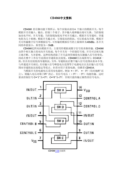
当模拟开关的电源电压采用双电源时,例如 =﹢5V, =﹣5V(均对地0V 而 言),则输入电压对称于0V 的正、负信号电压(﹢5V~﹣5V)均能传输。这时 要求控制信号 C=“1”为+5V,C=“0”为-5V,否则只能传输正极性的信号电压。
CD4066引脚功能图
内部方框图
Absolute Maximum Ratings 绝对最大额定值:
5
=50pF(Figure 6)
0
RL=1.0kΩ, CL=50pF, (Figure 7)VOS(f) = ½ VOS(1.0 kHz)
6. VDD = 5.0V
0
8. VDD = 10V
0
8. VDD = 15V
5
Signal
Input
CIS Capacitance 信 号
8.
输入电容
0
Signal
20
80 240
320
0
Δ“ON”
RL = 10kΩ to (VDD − VSS/2) VCC = VDD, VIS = VSS to VDD
ΔRO Resistance
VDD = 10V
10
N Between Any 2
MMBTRA221SS中文资料

元器件交易网
MMBTRA221SS...MMBTRA226SS
Io - V I(ON)
-500 -300
OUTPUT CURRENT Io (mA)
Io - VI(ON)
-500 -300
OUTPUT CURRENT Io (mA)
MMBTRA225SS Vo=-0.3V
Dated : 20/10/2005
元器件交易网
MMBTRA221SS...MMBTRA226SS
Characteristics at Tamb=25 OC Symbol Output Cut-off Current at -VO=30V DC Current Gain at -VO=5V, -IO=50mA MMBTRA221SS~226SS MMBTRA221SS MMBTRA222SS MMBTRA223SS MMBTRA224SS MMBTRA225SS MMBTRA226SS Output Voltage at -IO=10mA, -II=0.5mA Input Voltage (ON) at -VO=0.3V, -IO=20mA MMBTRA221SS~226SS MMBTRA221SS MMBTRA222SS MMBTRA223SS MMBTRA224SS MMBTRA225SS MMBTRA226SS Input Voltage (OFF) at -VO=5V, -IO=0.1mA Transition Frequency at -VO=10V, -IO=5mA, Input Current at -VI=5V MMBTRA221SS~224SS MMBTRA225SS~226SS MMBTRA221SS~226SS MMBTRA221SS MMBTRA222SS MMBTRA223SS MMBTRA224SS MMBTRA225SS MMBTRA226SS
SS22S中文资料

New ProductSS22S, SS23S & SS24SVishay General Semiconductor Document Number: 89008For technical questions within your region, please contact one of the following:Surface Mount Schottky Barrier RectifierFEATURES•Low profile package•Ideal for automated placement•Low forward voltage drop, low power losses•High efficiency•High surge capability•Meets MSL level 1, per J-STD-020, LF maximumpeak of 260 °C•Solder dip 260 °C, 40 s•Component in accordance to RoHS 2002/95/ECand WEEE 2002/96/ECTYPICAL APPLICATIONSFor use in low voltage, high frequency inverters,freewheeling, dc-to-dc converters, and polarityprotection applications.(Note: These devices are not Q101 qualified.)MECHANICAL DATACase: DO-214AC (SMA)Epoxy meets UL 94V-0 flammability ratingTerminals: Matte tin plated leads, solderable perJ-STD-002 and JESD22-B102E3 suffix for commercial grade, meets JESD 201 class1A whisker testPolarity:Color band denotes the cathode endPRIMARY CHARACTERISTICSI F(AV)2 AV RRM20 V, 30 V, 40 VI FSM40 AV F at I F = 2.0 A0.517 VT J max.150 °CDO-214AC (SMA)MAXIMUM RATINGS (T A = 25°C unless otherwise noted)PARAME ER SYMBOLSS22S SS23S SS24S UNITDevice marking code 22S23S24S VMaximum repetitive peak reverse voltage V RRM 203040VMaximum average forward rectified current (Fig. 1) I F(AV) 2.0 A Peak forward surge current 10 ms single half sine-wavesuperimposed on rated loadI FSM 40 AVoltage rate of change (rated V R) dV/dt10000V/µsOperating junction and storage temperature range T J, T STG- 55 to + 150 °C元器件交易网New ProductSS22S, SS23S & SS24SVishay General Semiconductor For technical questions within your region, please contact one of the following:Document Number: 89008Note:(1) Pulse test: 300 µs pulse width, 1 % duty cycleNote :(1) P.C.B. mounted with 0.4 x 0.4" (10 x 10 mm) copper pad areasRATINGS AND CHARACTERISTICS CURVES (T A = 25 °C unless otherwise noted)ELECTRICAL CHARACTERISTICS (T A = 25°C unless otherwise noted)PARAME ER T ES T CONDI T IONS SYMBOL T YP MAX.UNI TInstantaneous forward voltage (1) I F = 1 A,I F = 2 A,T J = 25 °C V F 0.4360.517-0.55V Reverse current (1)rated V R T J = 25 °C T J = 100 °CI R131.652008µA mA Typical junction capacitance 4.0 V , 1 MHzC J 130-pFTHERMAL CHARACTERISTICS (T A = 25°C unless otherwise noted)PARAME ER SYMBOL SS22S SS23S SS24S UNI TTypical thermal resistance (1) R θJA R θJL7525°C/WORDERING INFORMATION (Example)PREFERRED P/N UNIT WEIGHT (g)PREFERRED PACKAGE CODEBASE QUANTITYDELIVERY MODESS24S-E3/61T 0.06461T 18007" diameter plastic tape and reel SS24S-E3/5A T0.0645AT750013" diameter plastic tape and reelFigure 1. Forward Current Derating Curve Figure2. Forward Power Loss Characteristics元器件交易网New ProductSS22S, SS23S & SS24SVishay General SemiconductorDocument Number: 89008For technical questions within your region, please contact one of the following: PACKAGE OUTLINE DIMENSIONS in inches (millimeters)Figure3. Maximum Non-Repetitive Peak Forward Surge CurrentFigure4. Typical Instantaneous Forward CharacteristicsFigure5. Typical Reverse Leakage CharacteristicsFigure6. Typical Junction Capacitance元器件交易网Legal Disclaimer NoticeVishay Document Number: NoticeSpecifications of the products displayed herein are subject to change without notice. Vishay Intertechnology, Inc., or anyone on its behalf, assumes no responsibility or liability for any errors or inaccuracies.Information contained herein is intended to provide a product description only. No license, express or implied, by estoppel or otherwise, to any intellectual property rights is granted by this document. Except as provided in Vishay's terms and conditions of sale for such products, Vishay assumes no liability whatsoever, and disclaims any express or implied warranty, relating to sale and/or use of Vishay products including liability or warranties relating to fitness for a particular purpose, merchantability, or infringement of any patent, copyright, or other intellectual property right.The products shown herein are not designed for use in medical, life-saving, or life-sustaining applications.Customers using or selling these products for use in such applications do so at their own risk and agree to fully indemnify Vishay for any damages resulting from such improper use or sale.元器件交易网。
SS12SDP2;SS22SDP2;SS14MDP2;SS12SDH2;SS12SBP2;中文规格书,Datasheet资料
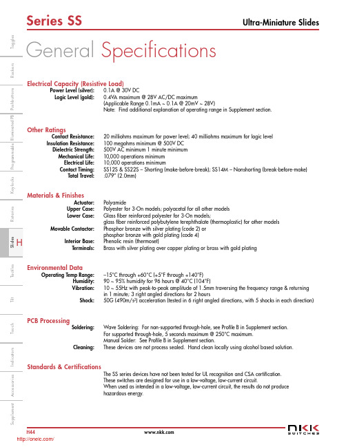
Series SSUltra-Miniature SlidesH44I n d i c a t o r sA c c e s s o r i e sS u p p l e m e n t T a c t i l e sK e y l o c k sR o t a r i e s P u s h b u t t o n sI l l u m i n a t e d P B P r o g r a m m a b l e R o c k e r sT o u c hT i l t T o g g l e sElectrical Capacity (Resistive Load)Power Level (silver): 0.1A @ 30V DCLogic Level (gold):0.4VA maximum @ 28V AC/DC maximum(Applicable Range 0.1mA ~ 0.1A @ 20mV ~ 28V)Note: Find additional explanation of operating range in Supplement section.Other RatingsContact Resistance: 20 milliohms maximum for power level; 40 milliohms maximum for logic level Insulation Resistance: 100 megohms minimum @ 500V DC Dielectric Strength: 500V AC minimum 1 minute minimum Mechanical Life: 10,000 operations minimum Electrical Life: 10,000 operations minimumContact Timing:SS12S & SS22S – Shorting (make-before-break); SS14M – Nonshorting (break-before-make)Total Travel: .079” (2.0mm)Materials & FinishesActuator: PolyamideUpper Case: Polyester for 3-On models; polyacetal for all other models Lower Case:Glass fiber reinforced polyester for 3-On models;glass fiber reinforced polybutylene terephthalate (thermoplastic) for other models Movable Contactor:Phosphor bronze with silver plating (code 2) orphosphor bronze with gold plating (code 4) Interior Base: Phenolic resin (thermoset)Terminals: Brass with silver plating over copper plating or brass with gold platingEnvironmental DataOperating Temp Range:–15°C through +60°C (+5°F through +140°F) Humidity: 90 ~ 95% humidity for 96 hours @ 40°C (104°F)Vibration:10 ~ 55Hz with peak-to-peak amplitude of 1.5mm traversing the frequency range & returning in 1 minute; 3 right angled directions for 2 hoursShock: 50G (490m/s 2) acceleration (tested in 6 right angled directions, with 5 shocks in each direction)PCB ProcessingSoldering:Wave Soldering: For non-supported through-hole, see Profile B in Supplement section. For supported through-hole, 5 seconds maximum @ 250°C maximum.Manual Solder: See Profile B in Supplement section.Cleaning: These devices are not process sealed. Hand clean locally using alcohol based solution.Standards & CertificationsThe SS series devices have not been tested for UL recognition and CSA certification. These switches are designed for use in a low-voltage, low-current circuit.When used as intended in a low-voltage, low-current circuit, the results do not producehazardous energy.General Specifications/Series SSUltra-Miniature Slides H45I n d i c a t o r sA c c e s s o r i e s S u p p l e m e n t T a c t i l e s Ke y l o c k s R o t a r i e s P u s h b u t t o n sI l l u m i n a t e d P B P r o g r a m m a b l e R o c k e r sT o u c h T i l t T o g g l e sTop or side actuation permits flexible board pact dimensions and low profile allow high density mounting and close stacking of PC boards.Crisp actuation positively indicates circuit status.Double molded thermoset base and thermo- plastic housing prevent loosening of terminals due to high soldering temperatures.Award-winning STC mechanism with benefitsunavailable in conventional mechanisms: smoother, positive detend actuation, increased contact stability, and unparalleled logic-level reliability. (Additional STC details in Terms and Acronyms in the Supplement section.)Insert molded terminals lock out flux, solvents, and other contaminants.Inch or metric terminal spacing for standard PC board grid (.100” x .100” or 2.0mm x 2.0mm).Actual SizeDistinctive Characteristics/Series SSUltra-Miniature SlidesH46I n d i c a t o r sA c c e s s o r i e sS u p p l e m e ntT a c t i l e sK e y l o c k sR o t a r i e s P u s h b u t t o n s I l l u m i n a t e d P BP r o g r a m m a b l e R o c k e r sT o u c hT i l t T o g g l e sTYPICAL SWITCH ORDERING EXAMPLESPDT ON-NONE-ON Circuit Terminals with .100” SpacingTop ActuatedSilver Contacts Rated 0.1A @ 30V DCDESCRIPTION FOR TYPICAL ORDERING EXAMPLESS12SDP2* 14M SP3T ON ON ON SS14M model has nonshorting contacts.22SDPDTONNONEONSS22S model has shorting contacts.See Poles & Circuits chart below.* 14M Circuit with silver contacts only./Series SSUltra-Miniature Slides H47I n d i c a t o r sA c c e s s o r i e sS u p p l e m e n t T a c t i l e s K e y l o c k sR o t a r i e sP u s h b u t t o nsI l l u m i n a t e d P BP r o g r a m m a b l e R o c k e rsT o u c h T il tT o g g l e sTERMINAL SPACINGCONTACT MATERIALS & RATINGSComplete explanation of operating range in Supplement section.2Gold over Silver/Phosphor Bronze Logic Level0.4VA max @ 28V AC/DC maxSilver over Phosphor Bronze Power Level 0.1A @ 30V DC4PSide ActuatedTop ActuatedHACTUATIONBInch .100” x .100” with Gray BaseMetric 2.0mm x 2.0mm with Black BaseDOn-None-On Single Pole Models On-None-On Double Pole Models 3-On ModelsOn-None-On Single Pole Models On-None-On Double Pole Models3-On Models.079.100.157/Series SSUltra-Miniature SlidesH48I n d i c a t o r sA c c e s s o r i e sS u p p l e m e n tT a c t i l e sK e y l o cksR o t a r i esP u s h b u t t o nsI l l u m i n a t e d P BP r o g ra m m ab l e R oc k e r sT o u c hT i l tT o g g le sTYPICAL SWITCH DIMENSIONSTop ActuatedSingle & Double PoleSide Actuated Single & Double PoleSS12SDP2SS12SDH23-On Circuit • Top Actuated Single PoleSS14MDP2SS14MDH2.079.0793-On Circuit • Side Actuated Single Pole/分销商库存信息:NKK-SWITCHSS12SDP2SS22SDP2SS14MDP2 SS12SDH2SS12SBP2SS22SDH2 SS22SBP2SS22SBH2SS14MDH2 SS14MBP2SS12SBH4SS22SDH4 SS12SBH2SS12SBP4SS12SDH4 SS12SDP4SS22SBP4。
- 1、下载文档前请自行甄别文档内容的完整性,平台不提供额外的编辑、内容补充、找答案等附加服务。
- 2、"仅部分预览"的文档,不可在线预览部分如存在完整性等问题,可反馈申请退款(可完整预览的文档不适用该条件!)。
- 3、如文档侵犯您的权益,请联系客服反馈,我们会尽快为您处理(人工客服工作时间:9:00-18:30)。
NUMBER OF CYCLES AT 60Hz
FIG.5 - TYPICAL REVERSE CHARACTERISTICS REVERSE CURRENT, MICROAMPERES
10 TJ = 100 °C
FORWARD CURRENT, AMPERES
Pulse Width = 300 µs 2% Duty Cycle TJ = 25 °C 10
1 cm
FIG.2 - DERATING CURVE FOR OUTPUT RECTIFIED CURRENT AVERAGE FORWARD OUTPUT CURRENT, AMPERES
2.5 75
FIG.3 - MAXIMUM NON-REPETITIVE PEAK FORWARD SURGE CURRENT PEAK FORWARD SURGE CURRENT, AMPERES
CJ TJ TSTG
Notes :
( 1 ) Reverse Recovery Test Conditions : IF = 0.5 A, IR = 1.0 A, Irr = 0.25 A. ( 2 ) Measured at 1.0 MHz and applied reverse voltage of 4.0 VDC
Rating at 25 ° C ambient temperature unless otherwise specified. Single phase, half wave, 60 Hz, resistive or inductive load. For capacitive load, derate current by 20%.
MAXIMUM RATINGS AND ELECTRICAL CHARACTERISTICS
RATING
Maximum Recurrent Peak Reverse Voltage Maximum RMS Voltage Maximum DC Blocking Voltage Maximum Average Forward Current Ta = 55 °C Peak Forward Surge Current, 8.3ms Single half sine wave Superimposed on rated load (JEDEC Method) Maximum Peak Forward Voltage at IF = 2.0 A. Maximum DC Reverse Current at Rated DC Blocking Voltage Ta = 25 °C Ta = 100 °C
8.3 ms SINGLE HALF SINE WAVE 60 Ta = 50 °C
2.0
1.5
45
1.0
30
0.5 60Hz RESISTIVE OR INDUCTIVE LOAD 0
15
0 0 25 50 75 100 125 150 175 1 2 4 6 10 20 40 60 100
AMBIENT TEMPERATURE, ( °C) FIG.4 - TYPICAL FORWARD CHARACTERISTICS
FORWARD VOLTAGE, VOLTS
SYMBOL
SS2A
SS2B
SS2C
SS2D
SS2E
SS2G
SS2J
SS2K SS2M
UNIT
VRRM VRMS VDC IF(AV)
50 35 50
100 70 100
150 105 150
200 140 200
300 210 300 2.0
400 280 400
600 420 600
800 560 800
UPDATE : JULY 24, 1998
元器件交易网
RATING AND CHARACTERISTIC CURVES ( SS2A - SS2M )
FIG.1 - REVERSE RECOVERY TIME CHARACTERISTIC AND TEST CIRCUIT DIAGRAM
1000 Volts 700 Volts Amps. 1000 Volts
IFSM VF IR IR(H)
Trr
75 0.95 5 50 35 50 - 65 to + 150 - 65 o + 150 1.4 1.7
Amps. Volts µA µA ns pf °C °C
Maximum Reverse Recovery Time ( Note 1 ) Typical Junction Capacitance ( Note 2 ) Junction Temperature Range Storage Temperature Range
1.0
SS2A - SS2D 1.0
SS2E - SS2G
0.1 TJ = 25 °C
SS2J - SS2M
0.1
0.01
0
20
40
60
80
100
120
140
PERCENT OF RATED REVERSE VOLTAGE, (%)
0.01 0 0.2 0.4 0.6 0.8 1.0 1.2 1.4 1.6 1.8 2.0
元器件交易网
SS2A - SS2M
PRV : 50 - 1000 Volts Io : 2.0 Amperes
FEATURES :
* * * * * * High current capability High surge current capability High reliability Low reverse current Low forward voltage drop Super fast recovery time
50 Ω 10 Ω + 0.5 A D.U.T. 50 Vdc (approx) 1Ω 0 PULSE GENERATOR ( NOTE 2 ) OSCILLOSCOPE ( NOTE 1 ) - 0.25 Trr
+
- 1.0 A SET TIME BASE FOR 15 ns/cm
NOTES : 1. Rise Time = 7 ns max., Input Impedance = 1 megaohm, 22 pF. 2. Rise time = 10 ns max., Source Impedance = 50 ohms. 3. All Resistors = Non-inductive Types.
SURFACE MOUNT SUPER FAST RECTIFIERS
SMB (DO-214AA)
1.1 ± 0.3
5.4 ± 0.15
4.8 ± 0.15
2.0 ± 0.1 3.6 ± 0.15 2.3 ± 0.2
0.22 ± 0.07
MECHANICAL DATA :
* Case : SMB Molded plastic * Epoxy : UL94V-O rate flame retardant * Lead : Lead Formed for Surface Mount * Polarity : Color band denotes cathode end * Mounting position : Any * Weight : 0.093 gram Dimensions in millimeter