FJV3105RMTF;中文规格书,Datasheet资料
全系列产品电子样本
上海奉申制冷控制器有限公司
MP45 系列小型压力控制器是一种用压力信号来控制的电开关,它是以压缩机的排气压力 为动作信号来控制压缩机的启停,当压缩机的排气压力超过调定值时,切断电源,起到压 力保护作用。
型号说明
型号
MP45
F
01
B
11
D
3
T
2.6
说明
型号代码 MP45M 为手动复 位形式
连接形式 代号 W
额定电压(V)
额定电流(A) 非诱导电流
诱导电流
满载电流 瞬时电流
A.C. 110
24 24 144
A.C.220
16 16 96
○1 : 公共触点 ○1 -○3 : 温度上升时闭合 ○1 -○5 :温度下降时闭合
↑M: 手动复位方向
版权归上海奉申制冷控制器有限公司所有,翻版必究! 网址:
自动
1.2 1.05
0.5→3.0 0.5→3.0
0.50~1.0 0.3~0.5
固定
自动 自动
2.0 1.5 2.0 1.5
0.5→3.0 固定≥0.4
手动
2.0 ≤1.6
0.3~0.5
0.5→3.0
自动 自动 0.3 0.2 2.0 1.5
固定
0.5→3.0 固定≥0.4 自动 手动 0.3 0.2 2.0 ≤1.6
标准附件及尺寸
版权归上海奉申制冷控制器有限公司所有,翻版必究! 网址:
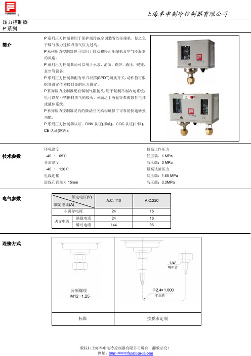
压力控制器 P 系列
触点形式
形式
低压
型号 P2,P3,P6,P10
P6M
复位形式 自动 手动
P12D,P16D,P20D,P30D
自动
上海奉申制冷控制器有限公司
施耐德 ATV310H075N4 三相变频器Easy Altivar 310 数据表

Product data sheetCharacteristicsATV310H075N4ATV310 三相400V 0,75 kw产品状态停止销售 : 四月 02, 2021i 停止销售主要信息产品系列Easy Altivar 310产品类型变频器应用领域简易机械组装方式带散热片产品短名ATV310电网相数三相额定电源电压 [Us]380...460 V - 15...10 %电动机功率 (kW)0.75 KW 适用 重载电机功率1 Hp 适用 重载补充信息产品应用场景异步电机每套数量"一套 1 只"EMC 滤波器无EMC 滤波器供电频率50/60 Hz +/- 5 %通讯端口协议串口Modbus端口类型RJ45 (前面板) 适用 串口Modbus 物理接口2线制RS485 适用 串口Modbus 传输帧RTU 适用 串口Modbus 传输率4800 bit/s 9600 bit/s 19200 bit/s 38400 bit/s地址数1…247 适用 串口Modbus 通讯服务读保持寄存器 (03) 29字 写单寄存器(06) 29字 写多寄存器 (16) 27字 读/写多个寄存器 (23) 4/4字 读设备标识 (43)线路电流 3.5 A 在…上 380 V (重载) 3.1 A 在…上 460 V (重载)视在功率 2.5 KVA 在…上 460 V (重载)预期线路Isc 5 KA 连续输出电流 2.3 A 重载最大瞬变电流 3.5 A 在 60 s (重载)功耗W28.8 W, at In (重载)变频器输出频率0.5…400 Hz 额定开关频率 4 kHz开关频率2...12 kHz 可调T h e i n f o r m a t i o n p r o v i d e d i n t h i s d o c u m e n t a t i o n c o n t a i n s g e n e r a l d e s c r i p t i o n s a n d /o r t e c h n i c a l c h a r a c t e r i s t i c s o f t h e p e r f o r m a n c e o f t h e p r o d u c t s c o n t a i n e d h e r e i n .T h i s d o c u m e n t a t i o n i s n o t i n t e n d e d a s a s u b s t i t u t e f o r a n d i s n o t t o b e u s e d f o r d e t e r m i n i n g s u i t a b i l i t y o r r e l i a b i l i t y o f t h e s e p r o d u c t s f o r s p e c i f i c u s e r a p p l i c a t i o n s .I t i s t h e d u t y o f a n y s u c h u s e r o r i n t e g r a t o r t o p e r f o r m t h e a p p r o p r i a t e a n d c o m p l e t e r i s k a n a l y s i s , e v a l u a t i o n a n d t e s t i n g o f t h e p r o d u c t s w i t h r e s p e c t t o t h e r e l e v a n t s p e c i f i c a p p l i c a t i o n o r u s e t h e r e o f .N e i t h e r S c h n e i d e r E l e c t r i c I n d u s t r i e s S A S n o r a n y o f i t s a f f i l i a t e s o r s u b s i d i a r i e s s h a l l b e r e s p o n s i b l e o r l i a b l e f o r m i s u s e o f t h e i n f o r m a t i o n c o n t a i n e d h e r e i n .速度范围1 (20)瞬时过转矩170…200 % 额定电机转矩取决于驱动器的额定值和电机类型制动力矩高达150%的额定电动机的扭矩 带有高惯量制动电阻器达到70%的电机转矩 不带制动电阻器异步电机控制配置文件二次电压/频率比无传感器的通量矢量控制节能比电机滑差补偿可调出厂预置输出电压380...460 V 三相电气连接端子, 夹紧力: 1.5...2.5 mm² (L1, L2, L3, PA/+, PB, U, V, W)紧固力矩0.8…1 N.M隔离电源与控制之间的电路电源内部电源 用于参考电位计: 5 V (4.75…5.25 V)直流, <10 mA 和 过载和短路保护内部电源 用于逻辑输入: 24 V (20.4…28.8 V)直流, <100 mA 和 过载和短路保护模拟量输入数量1模拟量输入类型可配置电流 AI1 0...20 mA 250 Ω可配置的电压 AI1 0...10 V 30 kOhm可配置的电压 AI1 0...5 V 30 kOhm离散量输入数量4数字量输入类型可编程 LI1...LI4 24 V 18...30 V离散量输入逻辑负逻辑 (漏), > 16 V (状态 0), < 10 V (状态 1), 输入阻抗 3.5 kOhm正逻辑(源), 0...< 5 V (状态 0), > 11 V (状态 1)采样期间10 Ms 适用 模拟量输入20 Ms, 公差 +/- 1 ms 适用 逻辑输入线性度误差‘+/- 0.3 % 最大值 适用 模拟量输入模拟量输出数量1模拟量输出 型号AO1 软件-可配置电压: 0...10 V, 阻抗: 470 Ω, 分辨率 8 位AO1 软件-可配置电流: 0...20 mA, 阻抗: 800 Ω, 分辨率 8 位离散量输出数量2输出型式逻辑输出 LO+, LO-继电器输出保护 R1A, R1B, R1C 1 C/O最小开关电流 [Imin]5 MA 在…上 24 V 直流 适用 逻辑继电器最大开关电流2 A 在…上 250 V AC 在…上 感性负载 量 cos phi = 0.4 L/R = 7 ms 适用 逻辑继电器2 A 在…上 30 V 直流 在…上 感性负载 量 cos phi = 0.4 L/R = 7 ms 适用 逻辑继电器3 A 在…上 250 V AC 在…上 阻性(负载) 量 cos phi = 1 L/R = 0 ms 适用 逻辑继电器4 A 在…上 30 V 直流 在…上 阻性(负载) 量 cos phi = 1 L/R = 0 ms 适用 逻辑继电器加速和减速倾斜S线性范围为0 - 999.9SU制动至停止采用直流注入, <30 s保护类型线路电源过压总线供电欠压输出相线和接地之间的过流过热保护电机各相线之间短路防止三相输入相损失电机热保护通过驱动连续计算I²T频率分辨率模拟量输入: A/D 转换器, 10 位显示单元: 0.1 Hz时间常量20 Ms +/- 1 ms 用于型号更改操作位置垂直方向 +/- 10°高度130 Mm宽度72 Mm深度143 Mm净重0.8 Kg环境电磁兼容性抗快速瞬变 - test level: 级别 4 conforming to IEC 61000-4-4静电放电抗干扰 - test level: 级别 3 conforming to IEC 61000-4-2免于传导干扰 - test level: 级别 3 conforming to IEC 61000-4-6射频电磁场辐射抗扰度试验 - test level: 级别 3 conforming to IEC 61000-4-3电压下降与断路抑制测试 conforming to IEC 61000-4-11浪涌放电抗干扰 - test level: 级别 3 conforming to IEC 61000-4-5符合标准IEC 61800-3IEC 61800-5-1IP 保护等级IP20 上部不带盲板IP41 上边距污染等级 2 符合 IEC 61800-5-1环境特征尘土污染抵抗 等级3C2 符合 IEC 60721-3-3化学污染抵抗 等级3C3 符合 IEC 60721-3-3抗冲击15 gn 适用 11 ms 符合 IEC 60068-2-27相对湿度5…95 % 无凝结 符合 IEC 60068-2-35…95 % 无滴水 符合 IEC 60068-2-3贮存环境温度-25…70 °C环境温度-10…55 °C 无降容55…60 °C 取下变频器顶部的保护盖 电流降额 2.2 %/ °C工作海拔<= 1000 m 无降容包装单位Unit Type of Package 1PCENumber of Units in Package 11合同保修保修单18 个月尺寸图尺寸尺寸 (in.)安装和间隙安装建议间距安装类型安装类型 A安装类型 B拆除变频器顶部的保护盖。
NUD3105LT1G;NUD3105LT1;中文规格书,Datasheet资料

• Industrial:Small Appliances, Security Systems, Automated Test
Equipment, Garage Door Openers
• Automotive: 5.0 V Driven Relays, Motor Controls, Power Latches,
DYNAMIC CHARACTERISTICS
Ciss
Input Capacitance
(VDS = 5.0 V,VGS = 0 V, f = 10 kHz)
Coss
Output Capacitance (VDS = 5.0 V, VGS = 0 V, f = 10 kHz)
Crss
Transfer Capacitance
Single Pulse Drain−to−Source Avalanche Energy (TJinitial = 25°C) (Note 2) Repetitive Pulse Zener Energy Limit (DC v 0.01%) (f = 100 Hz, DC = 0.5)
Junction Temperature
Drain (3)
Gate (1)
1.0 k 300 k
Gate (2)
1.0 k 300 k
1.0 k 300 k
CASE 318
Source (2)
ห้องสมุดไป่ตู้
Source (1)
Source (4)
CASE 318F
Figure 1. Internal Circuit Diagrams
Gate (5)
MAXIMUM RATINGS (TJ = 25°C unless otherwise specified)
VRF150;中文规格书,Datasheet资料

The VRF150 is a gold-metallized silicon n-channel RF power transistor de-signed for broadband commercial and military applications requiring high power and gain without compromising reliability, ruggedness, or inter-modulationdistortion.FEATURES• Improved Ruggedness V (BR)DSS = 170V• 150W with 11dB Typical Gain @ 150MHz, 50V• 150W with 18dB Typical Gain @ 30MHz, 50V • Excellent Stability & Low IMD • Common Source Con fi guration • Available in Matched Pairs• 30:1 Load VSWR Capability at Speci fi ed Operating Conditions • Nitride Passivated• Refractory Gold Metallization• High Voltage Replacement for MRF150• RoHS CompliantSymbol ParameterVRF150(MP)Unit V DSS Drain-Source Voltage170V I D Continuous Drain Current @ T C = 25°C 16A V GS Gate-Source Voltage±40V P D Total Device dissipation @ T C = 25°C 300W T STG Storage Temperature Range -65 to 150°CT JOperating Junction Temperature200Maximum Ratings All Ratings: T C =25°C unless otherwise speci fi edStatic Electrical CharacteristicsSymbol ParameterMin Typ MaxUnit V (BR)DSS Drain-Source Breakdown Voltage (V GS = 0V, I D = 100mA)170180V V DS(ON)On State Drain Voltage (I D(ON) = 10A, V GS = 10V) 2.03.0I DSS Zero Gate Voltage Drain Current (V DS = 100V, V GS = 0V) 1.0mA I GSS Gate-Source Leakage Current (V DS = ±20V, V DS = 0V) 1.0μA g fs Forward Transconductance (V DS = 10V, I D = 5A)4.5mhos V GS(TH)Gate Threshold Voltage (V DS = 10V, I D = 100mA)2.93.64.4VMicrosemi Website - 050-4936 R e v F 9-201Thermal CharacteristicsSymbol CharacteristicMin TypMax Unit R θJCJunction to Case Thermal Resistance0.60°C/WCAUTION:These Devices are Sensitive to Electrostatic Discharge. Proper Handling Procedures Should Be Followed./VRF150(MP)Dynamic CharacteristicsSymbol Parameter Test ConditionsMinTyp MaxUnitC ISS Input Capacitance V GS = 0V 420pFC oss Output CapacitanceV DS = 50V 210C rssReverse Transfer Capacitancef = 1MHz35Class A CharacteristicsSymbol Test Conditions Min Typ Max UnitG PS V DD = 50V, I DQ = 3A, P out = 150W PEP , f1 = 30MHz, f2 = 30.001MHz20dBIMD (d3)-50IMD (d9-d13)-75Functional CharacteristicsSymbol ParameterMinTyp Max Unit G PS f 1 = 30MHz, f 2 = 30.001MHz, V DD = 50V, I DQ = 250mA, P out = 150W PEP 18 dB G PS f = 150MHz, V DD = 50V, I DQ = 250mA, P out = 150W11ηD f 1 = 30MHz, f 2 = 30.001MHz, V DD = 50V, I DQ = 250mA, P out = 150W PEP 50%IMD (d3)f 1 = 30MHz, f 2 = 30.001MHz, V DD = 50V, I DQ = 250mA, P out = 150W PEP 1-32dBcIMD (d11)f 1 = 30MHz, f 2 = 30.001MHz, V DD = 50V, I DQ = 250mA, P out = 150W PEP -60ψf 1 = 30MHz, f 2 = 30.001MHz, V DD = 50V, I DQ = 250mA, P out = 150W PEP 30:1VSWR - All Phase AnglesNo Degradation in Output Power1. To MIL-STD-1311 Version A, test method 2204B, Two Tone, Reference Each ToneMicrosemi reserves the right to change, without notice, the speci fi cations and information contained herein.050-4936 R e v F 9-20101110201 10 100 250101520253035101520253035110100V DS(ON ), DRAIN-TO-SOURCE VOLTAGE (V) FIGURE 1, Output CharacteristicsI D , D R A I N C U R R E N T (A )I D , D R A I N C U R R E N T (A )VDS , DRAIN-TO-SOURCE VOLTAGE (V) FIGURE 3, Capacitance vs Drain-to-Source VoltageC , C A P A C I T A N C E (p F )V DS , DRAIN-TO-SOURCE VOLTAGE (V) FIGURE 4, Forward Safe Operating AreaI D , D R A I N C U R R E N T (V )V GS , GATE-TO-SOURCE VOLTAGE (V) FIGURE 2, Transfer CharacteristicsTypical Performance Curves/−50−45−40−35−30−25−20VRF150(MP)50-4936 R e v F 9-20100.10.20.30.40.50.60.710-510-410-3 10-2 10 1.0Z θJ C , T H E R M A L I M P E D A N C E (°C /W )RECTANGULAR PULSE DURATION (seconds)Figure 5. Maximum Effective Transient Thermal Impedance Junction-to-Case vs Pulse Duration050100150200250300P out , OUTPUT POWER (WATTS PEP)Figure 6. IMD versus P OUTI M D , I N T E R M O D U L A T I O N D I S T O R T I O N (d B )O U T P U T P O W E R (W P E P )P out , INPUT POWER (WATTS PEP)Figure 7. P OUT versus P INTypical Performance Curves/050-4936 R e v F 9-2010RFC1RFC1, C2, C8 -- Arco 463 or equivalent C3 -- 25pF, Unelco C4 -- 0.1uF, CeramicC5 -- 1.0 uF, 15 WV Tantalum C6 -- 250pF, Unelco J101C7-- 25pF, Unelco J101C9 -- Arco 262 or equivalent C10 -- 0.05uF, CeramicC11 -- 15uF, 60WV Electrolytic+ 50VDBias 0-12VRF RF OutputC2, C5, C6 - C9 -- 0.1uF SMT C3 -- 200pF ATC 700C C4 -- 15pF, ATC 700CC10 -- 10uF, 100V ElectrolyticR1, R2 -- 51 7, 1 W Carbon R3 -- 3.3 7, 1 W Carbon T1 -- 9:1 Transformer T2 -- 1:9 Transformer30 MHz test Circuit150 MHz test Circuit/050-4936 R e v F 9-2010.5” SOE Package OutlineAll Dimensions are ± .005DIMINCHES MILLIMETERS MIN MAX MIN MAX A 0.0960.99024.3925.14B0.4650.51011.8212.95C 0.2290.275 5.82 6.98D 0.2160.235 5.49 5.96E0.0840.110 2.14 2.79H0.1440.178 3.66 4.52J 0.0030.0070.080.17K 0.43511.0M45° NOM 45° NOM Q 0.1150.130 2.93 3.30R 0.2460.255 6.25 6.47U0.7200.73018.2918.54Microsemi’s products are covered by one or more of U.S. patents 4,895,810 5,045,903 5,089,434 5,182,234 5,019,522 5,262,336 6,503,786 5,256,5834,748,103 5,283,202 5,231,474 5,434,095 5,528,058 6,939,743, 7,352,045 5,283,201 5,801,417 5,648,283 7,196,634 6,664,594 7,157,886 6,939,743 7,342,262 and foreign patents. US and Foreign patents pending. All Rights Reserved.Adding MP at the end of P/N speci fi es a matched pair where V GS(TH) is matched between the two parts. V TH values are marked on the devices per the following table.Code Vth Range Code 2Vth Range A 2.900 - 2.975M 3.650 - 3.725B 2.975 - 3.050N 3.725 - 3.800C 3.050 - 3.125P 3.800 - 3.875D 3.125 - 3.200R 3.875 - 3.950E 3.200 - 3.275S 3.950 - 4.025F 3.275 - 3.350T 4.025 - 4.100G 3.350 - 3.425W 4.100 - 4.175H 3.425 - 3.500X 4.175 - 4.250J 3.500 - 3.575Y 4.250 - 4.325K3.575 - 3.650Z4.325 - 4.400V TH values are based on Microsemi measurements at datasheet conditions with an accuracy of 1.0%./分销商库存信息: MICROSEMIVRF150。
3.5寸TFT液晶规格书
Contents TFT transmissive, Normally white 6 O’clock 54.66(W)X82.94(H)X2.3(T) 48.96(W) x 73.44(H) 320(H) x (R.G.B.) x480(W) HX8357B 262K LED NC 8080 system 8/16 bit parallel T.B.D.
TEL: 86-0755-23000930 FAX : 86-0755-23000936
Doc No: Rev.:
XC-T0353701 0 2012.03.26
6 of 23
深圳信创光电技术有限公司
SHEN ZHEN SHI SINGSTART OPTOELECTRONIC CO., .,LTD .,
Item Contrast ratio (Center point) Response Rising: Tr Time Falling:Tf White Color Chromaticit y (CIE 1931) Red Green Blue Hor Ver
Symbol C/R Tr Tf Wx Wy Rx Ry Gx Gy Bx By θL1 θR1 øU1 øD1
Min -0.3 -0.3 -10 -20 -
Max 3.3 Vcc+0.3 60 70 90%(Max60°C) 15
Unit V V °C °C Dot mA(each Led)
Doc No: Rev.:
XC-T0353701 0 2012.03.26
8 of 23
深圳信创光电技术有限公司
SHEN ZHEN SHI SINGSTART OPTOELECTRONIC CO., .,LTD .,
Altivar Easy 310 ATV310H075N4E 变速电机驱动商品说明书

Product datasheetCharacteristicsATV310H075N4Evariable speed drive ATV310 - 0.75 kW - 1 hp -380...460 V - 3 phaseMainRange of productAltivar Easy 310Product or component type Variable speed drive Product specific application Simple machine Assembly style With heat sink Device short name ATV310Network number of phases Three phase[Us] rated supply voltage 380...460 V (- 15...10 %)Motor power kW 0.75 kW Motor power hp1 hpComplementaryProduct destination Asynchronous motors Quantity per set Set of 1EMC filter Without EMC filter Supply frequency50/60 Hz +/- 5 %Communication port protocol ModbusConnector type RJ45 for Modbus on front face Physical interface 2-wire RS 485 for Modbus Transmission frame RTU for Modbus Transmission rate4800 bit/s 9600 bit/s 19200 bit/s 38400 bit/sNumber of addresses 1...247 addresses for ModbusCommunication serviceRead holding registers (03), messaging: 29 words Write single register (06), messaging: 29 words Write multiple registers (16), messaging: 27 wordsRead/write multiple registers (23), messaging: 4/4 words Read device identification (43)Line current 3.1 A Apparent power 2.5 kVA Prospective line Isc <= 5 kA Continuous output current2.3 A at 4 kHzi s c l a i m e r : T h i s d o c u m e n t a t i o n i s n o t i n t e n d e d a s a s u b s t i t u t e f o r a n d i s n o t t o b e u s e d f o r d e t e r m i n i n g s u i t a b i l i t y o r r e l i a b i l i t y o f t h e s e p r o d u c t s f o r s p e c i f i c u s e r a p p l i c a t i o n sMaximum transient current 3.5 A for 60 sPower dissipation in W28.83 W at InSpeed drive output frequency0.5...400 HzNominal switching frequency 4 kHzSwitching frequency 2...12 kHz (adjustable)Speed range 1 (20)Transient overtorque170...200 % of nominal motor torque depending on drive rating and type of motorBraking torque Up to 150 % of nominal motor torque with braking resistor at high inertiaUp to 70 % of nominal motor torque without braking resistorAsynchronous motor control profile Energy saving ratioQuadratic voltage/frequency ratioSensorless flux vector controlMotor slip compensation AdjustablePreset in factoryOutput voltage380...460 V three phaseElectrical connection 1.5...2.5 mm² at terminal L1, L2, L3, PA/+, PB, U, V, WTightening torque0.8...1 N.mInsulation Electrical between power and controlSupply Internal supply for reference potentiometer : 5 V (4.75...5.25 V) DC 10 mA with overload and short-circuit protectionInternal supply for logic inputs : 24 V (20.4...28.8 V) DC 100 mA with overload and short-circuitprotectionAnalogue input number1Analogue input type Configurable current (AI1) 0...20 mA, impedance 250 OhmConfigurable voltage (AI1) 0...10 V, impedance 30 kOhmConfigurable voltage (AI1) 0...5 V, impedance 30 kOhmDiscrete input number4Discrete input type24 V (18...30 V) programmable, at LI1...LI4 terminal(s)Discrete input logic Positive logic (source), 0...< 5 V (state 0), > 11 V (state 1)Negative logic (sink), > 16 V (state 0), < 10 V (state 1), input impedance 3.5 kOhmSampling duration10 ms for analogue input20 ms, tolerance +/- 1 ms for logic inputLinearity error+/- 0.3 % of maximum value for analogue inputAnalogue output number1Analogue output type AO1 software-configurable voltage : 0...10 V, impedance: 470 Ohm, resolution 8 bitsAO1 software-configurable current : 0...20 mA, impedance: 800 Ohm, resolution 8 bitsDiscrete output number2Discrete output type(LO+, LO-) logic output(R1A, R1B, R1C) protected relay output 1 C/OMinimum switching current 5 mA at 24 V DC for logic relayMaximum switching current 2 A at 250 V AC on inductive load (cos phi = 0.4 L/R = 7 ms) for logic relay2 A at 30 V DC on inductive load (cos phi = 0.4 L/R = 7 ms) for logic relay3 A at 250 V AC on resistive load (cos phi = 1 L/R = 0 ms) for logic relay4 A at 30 V DC on resistive load (cos phi = 1 L/R = 0 ms) for logic relayAcceleration and deceleration ramps SULinear from 0...999.9 sBraking to standstill By DC injection, <= 30 sProtection type Against input phase loss in three-phaseThermal motor protection via the drive by continuous calculation of I²tLine supply overvoltageLine supply undervoltageOvercurrent between output phases and earthOverheating protectionShort-circuit between motor phasesFrequency resolution Converter A/D, 10 bits for analog input0.1 Hz for display unitTime constant20 ms, tolerance +/- 1 ms for reference changeOperating position Vertical +/- 10 degreeHeight130 mmWidth72 mmDepth143 mmProduct weight0.7 kgEnvironmentElectromagnetic compatibility Voltage dips and interruptions immunity test conforming to EN/IEC 61000-4-11Electrical fast transient/burst immunity test (test level: level 4) conforming to EN/IEC 61000-4-4Electrostatic discharge immunity test (test level: level 3) conforming to EN/IEC 61000-4-2Immunity to conducted disturbances (test level: level 3) conforming to EN/IEC 61000-4-6Radiated radio-frequency electromagnetic field immunity test (test level: level 3) conforming to EN/IEC 61000-4-3Surge immunity test (test level: level 3) conforming to EN/IEC 61000-4-5Standards EN/IEC 61800-3EN/IEC 61800-5-1IP degree of protection IP41 on topIP20 without blanking plate on upper partPollution degree 2 conforming to EN/IEC 61800-5-1Environmental characteristic Chemical pollution resistance class 3C3 conforming to EN/IEC 60721-3-3Dust pollution resistance class 3S2 conforming to EN/IEC 60721-3-3Shock resistance15 gn (duration = 11 ms) conforming to EN/IEC 60068-2-27Relative humidity 5...95 % (without condensation) conforming to IEC 60068-2-35...95 % (without dripping water) conforming to IEC 60068-2-3Ambient air temperature for storage-25...70 °CAmbient air temperature for operation-10...55 °C without derating55...60 °C protective cover from the top of the drive removed with current derating 2.2 % per °C Operating altitude<= 1000 m without deratingDimensions Drawings DimensionsDimensions in mmDimensions in in.Mounting and ClearanceMounting RecommendationsClearanceMounting TypesMounting Type AMounting Type BRemove the protective cover from the top of the drive.Connections and SchemaThree-Phase Power Supply Wiring DiagramA1 :DriveKM1 :Contactor (only if a control circuit is needed)P1 : 2.2 kΩ reference potentiometer. This can be replaced by a 10 kΩ potentiometer (maximum). Q1 :Circuit breakerR :Braking resistor (optional)(1)Negative logic (Sink)(2)Positive logic (Source) (factory set configuration)(3)0...10 V or 0...20 mA(4)Line choke three-phase (optional)。
ERG1FGS301E中文资料(PANASONIC)中文数据手册「EasyDatasheet - 矽搜」

Type L
ERG(X)12S 6.35
ERG(X)1S 9.00
ERG(X)1F
ERG(X)2S ERG(X)2F
12.00
ERG(X)3S ERG(X)3F
15.00
ERG(X)5S ERG(X)5F
24.00
外形尺寸(mm)
φD
k
2.3
30.0
2.8
30.0
4.0
30.0
φd
0.65 0.65 0.80 0.80
120 –55 °C
100
80
60 Rated Load (%)
40
20
0 –60 –40 –20 0
70 °C
ERG(X)12S
ERG(X)1S, 1F ERG(X)2S, 2F ERG(X)3S, 3F
ERG(X)5S, 5F
130 °C
235 °C
20 40 60 80 100 120 140 160 180 200 220 240
½Z type isnon standard resistance values.
Code Type Res.Tol. Res. Value Range Code Type Res.Tol. Res. Value Range
±2 % 0.1 to 0.91 12S
±5 % 0.1 to 0.18 Z
The first two digitsare significant figures of resistance and the third one denotes number of zerosfollowing. Decimal point isexpressed by (Ex.) 1R0 : 1.0
NUD3105DMT1G;NUD3105DMT1;中文规格书,Datasheet资料

NUD3105DIntegrated Relay,Inductive Load DriverThis device is used to switch inductive loads such as relays, solenoids incandescent lamps, and small DC motors without the need of a free−wheeling diode. The device integrates all necessary items such as the MOSFET switch, ESD protection, and Zener clamps. It accepts logic level inputs thus allowing it to be driven by a large variety of devices including logic gates, inverters, and microcontrollers.Features•Provides a Robust Driver Interface Between D.C. Relay Coil and Sensitive Logic Circuits•Optimized to Switch Relays from 3.0 V to 5.0 V Rail •Capable of Driving Relay Coils Rated up to 2.5 W at 5.0 V•Internal Zener Eliminates the Need of Free−Wheeling Diode •Internal Zener Clamp Routes Induced Current to Ground for Quieter Systems Operation•Low V DS(on)Reduces System Current Drain•Pb−Free Package is AvailableTypical Applications•Telecom: Line Cards, Modems, Answering Machines, FAX •Computers and Office: Photocopiers, Printers, Desktop Computers •Consumer: TVs and VCRs, Stereo Receivers, CD Players, Cassette Recorders•Industrial: Small Appliances, Security Systems, Automated Test Equipment, Garage Door Openers•Automotive: 5.0 V Driven Relays, Motor Controls, Power Latches, Lamp DriversINTERNAL CIRCUIT DIAGRAMSCASE 318FDevice Package Shipping†ORDERING INFORMATIONMARKINGDIAGRAM Relay, Inductive Load Driver0.5 Amp, 8.0 V ClampNUD3105DMT1SC−743000/T ape & Reel SC−74CASE 318FSTYLE 7JW4= Specific Device CodeD= Date CodeG= Pb−Free Package†For information on tape and reel specifications, including part orientation and tape sizes, please refer to our Tape and Reel Packaging Specification Brochure, BRD8011/D.(Note: Microdot may be in either location)NUD3105DMT1G SC−74(Pb−Free)3000/T ape & Reel 6MAXIMUM RATINGS (T J= 25°C unless otherwise specified)Symbol Rating Value Unit V DSS Drain to Source Voltage − Continuous 6.0V dc V GS Gate to Source Voltage – Continuous 6.0V dcI D Drain Current – Continuous500mAE z Single Pulse Drain−to−Source Avalanche Energy (T Jinitial= 25°C)50mJT J Junction Temperature150°C T A Operating Ambient Temperature−40 to 85°C T stg Storage Temperature Range−65 to +150°CP D Total Power Dissipation (Note 1) Derating Above 25°C 3801.5mWmW/°CR q JA Thermal Resistance Junction−to−Ambient329°C/W Stresses exceeding Maximum Ratings may damage the device. Maximum Ratings are stress ratings only. Functional operation above the Recommended Operating Conditions is not implied. Extended exposure to stresses above the Recommended Operating Conditions may affect device reliability.1.This device contains ESD protection and exceeds the following tests:Human Body Model 2000 V per MIL_STD−883, Method 3015.Machine Model Method 200 V.TYPICAL ELECTRICAL CHARACTERISTICS (T J= 25°C unless otherwise noted)Symbol Characteristic Min Typ Max Unit OFF CHARACTERISTICSV BRDSS Drain to Source Sustaining Voltage (Internally Clamped)(I D = 10 mA)6.08.09.0VB VGSO I g = 1.0 mA−−8.0VI DSS Drain to Source Leakage Current(V DS = 5.5 V , V GS = 0 V, T J= 25°C)(V DS = 5.5 V, V GS = 0 V, T J= 85°C )−−−−1515m AI GSS Gate Body Leakage Current(V GS = 3.0 V, V DS = 0 V)(V GS = 5.0 V, V DS = 0 V)5.0−−−3565m AON CHARACTERISTICSV GS(th)Gate Threshold Voltage(V GS = V DS, I D = 1.0 mA)(V GS = V DS, I D = 1.0 mA, T J = 85°C)0.80.81.2−1.41.4VR DS(on)Drain to Source On−Resistance(I D = 250 mA, V GS = 3.0 V)(I D = 500 mA, V GS = 3.0 V)(I D = 500 mA, V GS = 5.0 V)(I D = 500 mA, V GS = 3.0 V, T J= 85°C)(I D = 500 mA, V GS = 5.0 V, T J= 85°C)−−−−−−−−−−1.21.30.91.30.9WI DS(on)Output Continuous Current(V DS = 0.25 V, V GS = 3.0 V)(V DS = 0.25 V, V GS = 3.0 V, T J = 85°C)300200400−−−mAg FS Forward Transconductance(V OUT = 5.0 V, I OUT = 0.25 A)350570−mMhosTYPICAL ELECTRICAL CHARACTERISTICS (T J= 25°C unless otherwise noted)Symbol UnitMaxTypMinCharacteristicDYNAMIC CHARACTERISTICSC iss Input Capacitance(V DS = 5.0 V,V GS = 0 V, f = 10 kHz)−25−pFC oss Output Capacitance(V DS = 5.0 V, V GS = 0 V, f = 10 kHz)−37−pFC rss Transfer Capacitance(V DS = 5.0 V, V GS = 0 V, f = 10 kHz)−8.0−pF SWITCHING CHARACTERISTICSSymbol Characteristic Min Typ Max Unitst PHL t PLH t PHL t PLH Propagation Delay Times:High to Low Propagation Delay; Figure 1 (5.0 V)Low to High Propagation Delay; Figure 1 (5.0 V)High to Low Propagation Delay; Figure 1 (3.0 V)Low to High Propagation Delay; Figure 1 (3.0 V)−−−−25804444−−−−nSt f t r t f t r Transition Times:Fall Time; Figure 1 (5.0 V)Rise Time; Figure 1 (5.0 V)Fall Time; Figure 1 (3.0 V)Rise Time; Figure 1 (3.0 V)−−−−23325330−−−−nS−Figure 1. Switching WaveformsV outGNDV inGNDV ZV CCV CCV Z , Z E N E R C L A M P V O L T A G E (V )11.012.010.09.08.07.013.00.10.20.30.40.50.60.70.8V DS , DRAIN TO SOURCE VOLTAGE (V)Figure 2. Output CharacteristicsV GS , GATE −TO −SOURCE VOLTAGE (V)Figure 3. Transfer FunctionTEMPERATURE (°C)Figure 4. On Resistance Variation vs. TemperatureFigure 5. R DS(ON) Variation withGate −To −Source VoltageFigure 6. Zener Voltage vs. Temperature I Z , ZENER CURRENT (mA)Figure 7. Zener Clamp Voltage vs. Zener CurrentI D , D R A I N C U R R E N T (A )−50−250255075100120010008006004002000125R D S (o n ), D R A I N −T O −S O U R C E R E S I S T A N C E (m W )V Z , Z E N E R V O L T A G E (V )−50−252550751001251.01.21.41.60.82.01.8R D S (o n ), D R A I N −T O −S O U R C E R E S I S T A N C E (W )1.0100.1100I D , D R A I N C U R R E N T (A )0.5 1.0 1.5 2.0 2.5 3.0 3.5 4.0 4.5 5.0V GS , GATE −TO −SOURCE VOLTAGE (V)TEMPERATURE (°C)101.00.10.010.0010.00010.0000110006.0V DS , DRAIN −TO −SOURCE VOLTAGE (V)0.01100100.10.11.00.01I D , D R A I N C U R R E N T (A )1.0I D , DRAIN CURRENT (A)Figure 8. On −Resistance vs. Drain Current andTemperatureTEMPERATURE (°C)Figure 9. Gate Leakage vs. TemperatureR D S (O N ), D R A I N −T O −S O U R C E R E S I S T A N C E (W )1.00.90.80.50.60.71.11.20.050.10.150.20.250.30.350.40.450.5I G S S , G A T E L E A K A G E (m A )302505103540−50−252550751001252015Figure 10. Safe Operating Area for NUD3105DLT1Figure 11. Transient Thermal Response for NUD3105DLT10.010.1 1.010100100010,000100,0001,000,000r (t ), T R A N S I E N T T H E R M A L R E S I S T A N C E (N O R M A L I Z E D )t1, PULSE WIDTH (ms)Designing with this Data Sheet1.Determine the maximum inductive load current (at max V CC , min coil resistance & usually minimum temperature) that the NUD3105D will have to drive and make sure it is less than the max rated current.2.For pulsed operation, use the Transient Thermal Response of Figure 11 and the instructions with it to determine the maximum limit on transistor power dissipation for the desired duty cycle and temperature range.e Figures 10 and 11 with the SOA notes to insure that instantaneous operation does not push the device beyond the limits of the SOA plot.4.Verify that the circuit driving the gate will meet the V GS(th) from the Electrical Characteristics table.ing the max output current calculated in step 1,check Figure 7 to insure that the range of Zener clamp voltage over temperature will satisfy all system & EMI requirements.e I GSS and I DSS from the ElectricalCharacteristics table to insure that “OFF” state leakage over temperature and voltage extremes does not violate any system requirements.7.Review circuit operation and insure none of the device max ratings are being exceeded.Figure 12. A 200 mW, 5.0 V Dual Coil Latching Relay Applicationwith 3.0 V Level Translating InterfaceAPPLICATIONS DIAGRAMSFigure 13. A 140 mW, 5.0 V Relay with TTL InterfaceMax Continuous Current Calculationfor TX2−5V Relay, R1 = 178 W Nominal @ R A = 25°C Assuming ±10% Make Tolerance,R1 = 178 W * 0.9 = 160 W Min @ T A = 25°C T C for Annealed Copper Wire is 0.4%/°CR1 = 160 W * [1+(0.004) * (−40°−25°)] = 118 W Min @ −40°C I O Max = (5.5 V Max − 0.25V) /118 W = 45 mA Figure 14. A Quad 5.0 V, 360 mW Coil Relay BankPACKAGE DIMENSIONSSC −74CASE 318F −05ISSUE MNOTES:1.DIMENSIONING AND TOLERANCING PER ANSI Y14.5M, 1982.2.CONTROLLING DIMENSION: INCH.3.MAXIMUM LEAD THICKNESS INCLUDES LEAD FINISH THICKNESS. MINIMUM LEAD THICKNESS IS THE MINIMUM THICKNESS OF BASE MATERIAL.4.318F −01, −02, −03, −04 OBSOLETE. NEW STANDARD 318F −05.ǒmm Ǔ*For additional information on our Pb −Free strategy and solderingdetails, please download the ON Semiconductor Soldering and Mounting Techniques Reference Manual, SOLDERRM/D.SOLDERING FOOTPRINT*DIM A MIN NOM MAX MINMILLIMETERS0.90 1.00 1.100.035INCHES A10.010.060.100.001b 0.250.370.500.010c 0.100.180.260.004D 2.90 3.00 3.100.114E 1.30 1.50 1.700.051e 0.850.95 1.050.0340.200.400.600.0080.0390.0430.0020.0040.0150.0200.0070.0100.1180.1220.0590.0670.0370.0410.0160.024NOM MAX 2.50 2.75 3.000.0990.1080.118H E −−L 0°10°0°10°qSTYLE 7:PIN 1.SOURCE 12.GATE 13.DRAIN 24.SOURCE 25.GATE 26.DRAIN 1ON Semiconductor and are registered trademarks of Semiconductor Components Industries, LLC (SCILLC). SCILLC reserves the right to make changes without further notice to any products herein. SCILLC makes no warranty, representation or guarantee regarding the suitability of its products for any particular purpose, nor does SCILLC assume any liability arising out of the application or use of any product or circuit, and specifically disclaims any and all liability, including without limitation special, consequential or incidental damages.“Typical” parameters which may be provided in SCILLC data sheets and/or specifications can and do vary in different applications and actual performance may vary over time. All operating parameters, including “Typicals” must be validated for each customer application by customer’s technical experts. SCILLC does not convey any license under its patent rights nor the rights of others. SCILLC products are not designed, intended, or authorized for use as components in systems intended for surgical implant into the body, or other applications intended to support or sustain life, or for any other application in which the failure of the SCILLC product could create a situation where personal injury or death may occur.Should Buyer purchase or use SCILLC products for any such unintended or unauthorized application, Buyer shall indemnify and hold SCILLC and its officers, employees, subsidiaries,affiliates, and distributors harmless against all claims, costs, damages, and expenses, and reasonable attorney fees arising out of, directly or indirectly, any claim of personal injury or death associated with such unintended or unauthorized use, even if such claim alleges that SCILLC was negligent regarding the design or manufacture of the part. SCILLC is an Equal Opportunity/Affirmative Action Employer. This literature is subject to all applicable copyright laws and is not for resale in any manner.PUBLICATION ORDERING INFORMATION分销商库存信息:ONSEMINUD3105DMT1G NUD3105DMT1。
- 1、下载文档前请自行甄别文档内容的完整性,平台不提供额外的编辑、内容补充、找答案等附加服务。
- 2、"仅部分预览"的文档,不可在线预览部分如存在完整性等问题,可反馈申请退款(可完整预览的文档不适用该条件!)。
- 3、如文档侵犯您的权益,请联系客服反馈,我们会尽快为您处理(人工客服工作时间:9:00-18:30)。
FJV3105RNPN Epitaxial Silicon TransistorAbsolute Maximum Ratings T a =25°C unless otherwise notedElectrical Characteristics T a =25°C unless otherwise notedSymbol ParameterValue Units V CBO Collector-Base Voltage 50V V CEO Collector-Emitter Voltage 50V V EBO Emitter-Base Voltage 10V I C Collector Current100mA P C Collector Power Dissipation 200mW T J Junction Temperature 150°C T STGStorage Temperature-55 ~ 150°CSymbol ParameterTest Condition Min.Typ.Max.Units BV CBO Collector-Base Breakdown Voltage I C =10µA, I E =050V BV CEO Collector-Emitter Breakdown Voltage I C =100µA, I B =050V I CBO Collector Cut-off Current V CB =40V, I E =00.1µAh FE DC Current GainV CE =5V, I C =5mA 30V CE (sat)Collector-Emitter Saturation Voltage I C =10mA, I B =0.5mA 0.3V C ob Output CapacitanceV CE =10V, I C =5mA f=1MHz3.7pF f T Current Gain Bandwidth Product V CE =10V, I C =5mA 250MHz V I (off)Input Off Voltage V CE =5V, I C =100µA 0.3V V I (on)Input On Voltage V CE =0.3V, I C =20mA2.5V R 1Input Resistor3.24.7 6.2K ΩR 1/R 2Resistor Ratio0.420.470.52FJV3105RSwitching Application (Bias Resistor Built In)•Switching circuit, Inverter, Interface circuit, Driver Circuit •Built in bias Resistor (R 1=4.7K Ω, R 2=10K Ω)•Complement to FJV4105REquivalent CircuitBECR1R2R25MarkingSOT-231. Base2. Emitter3. Collector123FJV3105RFJV3105RDISCLAIMERFAIRCHILD SEMICONDUCTOR RESERVES THE RIGHT TO MAKE CHANGES WITHOUT FURTHER NOTICE TO ANY PRODUCTS HEREIN TO IMPROVE RELIABILITY , FUNCTION OR DESIGN. FAIRCHILD DOES NOT ASSUME ANY LIABILITY ARISING OUT OF THE APPLICATION OR USE OF ANY PRODUCT OR CIRCUIT DESCRIBED HEREIN; NEITHER DOES IT CONVEY ANY LICENSE UNDER ITS PATENT RIGHTS, NOR THE RIGHTS OF OTHERS.TRADEMARKSThe following are registered and unregistered trademarks Fairchild Semiconductor owns or is authorized to use and is not intended to be an exhaustive list of all such trademarks.LIFE SUPPORT POLICYFAIRCHILD S PRODUCTS ARE NOT AUTHORIZED FOR USE AS CRITICAL COMPONENTS IN LIFE SUPPORTDEVICES OR SYSTEMS WITHOUT THE EXPRESS WRITTEN APPROVAL OF FAIRCHILD SEMICONDUCTOR CORPORATION.As used herein:1. Life support devices or systems are devices orsystems which, (a) are intended for surgical implant intothe body, or (b) support or sustain life, or (c) whosefailure to perform when properly used in accordancewith instructions for use provided in the labeling, can be reasonably expected to result in significant injury to the user.2. A critical component is any component of a life support device or system whose failure to perform can be reasonably expected to cause the failure of the life support device or system, or to affect its safety or effectiveness.PRODUCT STATUS DEFINITIONS Definition of Terms Datasheet Identification Product Status DefinitionAdvance InformationPreliminaryNo Identification Needed Obsolete This datasheet contains the design specifications for product development. Specifications may change in any manner without notice.This datasheet contains preliminary data, andsupplementary data will be published at a later date.Fairchild Semiconductor reserves the right to make changes at any time without notice in order to improve design.This datasheet contains final specifications. Fairchild Semiconductor reserves the right to make changes at any time without notice in order to improve design.This datasheet contains specifications on a product that has been discontinued by Fairchild semiconductor.The datasheet is printed for reference information only.Formative or In Design First ProductionFull ProductionNot In ProductionImpliedDisconnect ISOPLANARLittleFETMicroFETMicroPakMICROWIREMSXMSXProOCXOCXProOPTOLOGIC âOPTOPLANARFACT FACT Quiet Series FAST âFASTr FRFET GlobalOptoisolator GTO HiSeCI 2CRev. I1ACEx ActiveArray Bottomless CoolFET CROSSVOLT DOME EcoSPARK E 2CMOS TM EnSigna TMPACMANPOP Power247 PowerTrench âQFET QS QT Optoelectronics Quiet Series RapidConfigure RapidConnect SILENT SWITCHER âSMART START SPMStealthSuperSOT -3SuperSOT -6SuperSOT -8SyncFET TinyLogic TruTranslation UHC UltraFET âVCXAcross the board. Around the world. The Power FranchiseProgrammable Active Droop分销商库存信息: FAIRCHILDFJV3105RMTF。