735D158X0006C2中文资料
SEL-735_Datasheet_20111111

SEL-735 Power Quality and Revenue MeterThe SEL-735 meter combines leading power quality capabilities with exceptional revenue metering accuracy at an eco-nomical price. Power quality reports with IEC 61000-4-30 compliance help identify and troubleshoot problems in power system equipment. Advanced communications deliver critical and historical information in real-time to virtually any communications system. The SEL-735 is the essential meter for substation, power plant, and industrial metering. Features and Benefits■High Precision Revenue Metering Guarantee: 0.06%, 0.02% typical.■Capture every power quality disturbance with preconfigured logs and triggers.■Compare power quality measurements across the system with IEC 61000-4-30 power quality compliance.■Perform statistical calculations while reporting only critical information to save system bandwidth.■Standardize on one revenue meter for generation, transmission, distribution, intertie, main entrance, and submeter applications.■Deliver complete billing data to Itron® MV-90® software over any communications port.■Integrate into virtually any system with copper or fiber-optic Ethernet, serial, multidrop, infrared, or telephone modem communications.■Simultaneously communicate with ten other devices using industry standard protocols.2Three SEL-735 variants provide a meter for any application and any budget.A = IEC 61000-4-30 Class A compliant.S = IEC 61000-4-30 Class S compliant.One Package, Three Flexible SolutionsMetering, GeneralSEL-735Basic PQSEL-735Intermediate PQSEL-735Advanced PQStated list price $1,500$2,000$2,500Watt-hour Accuracy 0.06%0.06%0.06%V oltage Range 5–300 V L-N ,9–520 V L-L 5–300 V L-N ,9–520 V L-L 5–300 V L-N ,9–520 V L-L Current Range0.001–22 A 0.001–22 A 0.001–22 A Form Options (Elements) 5 and 9 (2,3) 5 and 9 (2,3) 5 and 9 (2,3)Load Profile Recorders x Channels 1 x 1612 x 1612 x 16Memory32 MB128 MB128 MBIEC 61000-4-30 Power QualitySEL-735Basic PQSEL-735Intermediate PQSEL-735Advanced PQMeasurement Aggregation10/12 Cycle IntervalsA A A 150/180 Cycles, 10 min., 120 min. Intervals –A A V oltage and CurrentA A A V oltage and Current Unbalance A A A Individual V oltage and Current Harmonics S S S V oltage and Current THDA A A Real, Reactive, and Apparent PowerAAAPower Quality ParametersReal-Time Clock S S S Frequency A A A Flicker–S S V oltage Dips, Swells, and Interruptions A A A V oltage and Current Interharmonics ––S Harmonic Power ––S Harmonic Phase Angles ––S Transient Detection––(future)Maximum Harmonic Order 15th63rd63rdWaveform CaptureSamples-per-cycle 1616 and 12816, 128, and 512Duration (cycles)1515, 30, 60, 120, 300, 60015, 30, 60, 120, 300, 600Number of Events 6416–31554–3155COMTRADE ReportsYYY3View a complete state of the power system using no-cost AC SEL ERATOR QuickSet® SEL-5030 Software. Quickly assemble an overview of the most important system parameters. Load profile trending displays voltage, current, power, and harmonicinformation. Record years of voltage, current, power, frequency, and harmonic information on a per-phase basis.Power Quality Measurements•IEC 61000-4-30 power quality compliant•Statistical trending of virtually any parameter, including:–Voltage and current –Frequency–Harmonics up to the 63rd–Total harmonic distortion (THD)–Unbalance—symmetrical components •Sags, swells, and interruptions •Flicker measurement•Waveform capture up to 512 samples/cycle •Transients (future addition)Power DashboardTOU stores and resets peak demand data Load Profile trends power draw and energy consumptionVoltage/Sag/Swell/Interruption reports system interruptions with 1 ms resolutionMeter monitoring software standard with the SEL-735Flicker and harmonics reports help locate system disturbances4High-Function Metering for Substations, Power Generation, and Industrial LoadsRevenue metering applications require a diverse set of features to cover both new and legacy metering requirements. The SEL-735 supports a large feature set to cover a wide range of metering needs.•4-Quadrant Metering•Multiple Load Profile Recorders•Time-of-Use Metering•Transformer/Line-Loss CompensationHigh Accuracy Metering for High Value Applications Many new metering installations, such as distributed generation, operate over a very large current range. The SEL-735 provides high accuracy over an extended operating range with a 0.06% Wh guarantee. Typical Wh accuracy errors of 0.02% betters the accuracy of many measurement standards.Simplified Setup and TroubleshootingFeature Overview•Use AC SEL ERATOR QuickSet to customize your metering. Set and edit meter configuration, settings, and logic.•View the HMI screens in AC SEL ERATOR QuickSet to check wiring connections, phase rotation, and power flow direction.•V oltage and current sequence elements allow fast troubleshooting of miswired installations.•Form 5, 3-Wire Delta and Form 9, 4-Wire Wye metering connections•ANSI C12.20 0.2 and IEC 62053-22 0, 2S accuracy class leading•Rack-mount, panel-mount, easily extractable meter (EXM), wall-mount, and NEMA enclosure options •Simultaneous Ethernet, EIA-485, EIA-232, telephone modem, and optical probe communications •Synchrophasor data with IEEE C37.118 accuracy (future release)•Enhanced SEL OGIC® control equations •Communication protocols–SEL ASCII–Modbus® RTU/TCP–SEL Fast Operate/Fast Meter–M IRRORED B ITS® communications–SEL Distributed Port Switch (LMD)–DNP3 Serial and LAN/WAN•Inputs/outputs–2 digital inputs, 3 electromechanical outputs–4 digital inputs, 4 KY outputs with programmable Ke–4 digital inputs, 4 electromechanical outputs–4 analog outputs, 4 KY outputs with programmable KeSee model option table for available configurations and options.5Advanced Display and ControlsProduct OverviewCT BoardIa, Ib, IcSEL provides a worldwide, ten-year product warranty—no questions asked.Custom nameplate, and bar code.Simple front-panel navigationRead, test, and program with ANSI Type II optical port.Power Supply Board2 Inputs3 OutputsCommunications BoardExpansion Slot #1EIA-485Telephone Modem EIA-232PT BoardVa, Vb, Vc, VnMain BoardEthernet EIA-232IRIG-BEIA-232/485I/O BoardExpansion Slot #24 Inputs4 Outputs (solid-state or electromechanical) or4 Analog Outputs 4 Solid-State OutputsSealing Provision Custom controls7Power Quality CapabilitiesMeasure and Record the Following:•IEC 61000-4-30 compliant current, voltage, power, energy,harmonic, flicker, and unbalance•Measurement aggregation in 10/12 cycle, 3-second*,10-minute*, and 120-minute intervals*•Harmonic angles for voltage and current*•High-resolution, 512 samples/cycle waveform capture*•Total harmonic distortion (THD), crest factor, and K-factormetering with up to 63rd harmonic content•High-speed load profile recording with three-secondresolution*•VSSI•Symmetrical components (unbalance)* Optional BenefitsVSSI RecorderCorrelate system disturbances with the voltagesag/swell/interruptions (VSSI) recorder. Enabled from the factory, the VSSI recorder time-stamps voltage excursions with up to 1 ms resolution and records indefinitely using an adaptive sampling rate. The SEL-735 stores and reportsresidual voltage, duration, affected phases, CBEMA/ITICreports, and time stamp of occurrence. The VSSI settingsinclude trigger thresholds from ±3% to ±100% of the actual value and automatic recording duration dependent on thelength of the voltage excursion. AC SEL ERATOR QuickSetautomatically graphs and analyzes VSSI data and includes an export feature. Applications with SCADA systems can also retrieve this data using the DNP3 protocol.Time-of-Use (TOU) MeteringRecord demand and energy consumption with a user-defined calendar; use TOU metering to bill consumption at different rates based on season, day type, and time of day. The program automatically self-reads and resets demand; there is no need to manually reset meters.Harmonic MeteringMonitor, record, and control using individual harmonicvalues, THD, and K-factor with resolution up to the 63rdharmonic.Interharmonic MeteringMeasure, record, and control using Group THD. Measureinterharmonics from 5Hz to 3800Hz in 5Hz bins.View event records andwaveform captures ofsystem anomalies.VSSI reports detail systeminterruptions with 1ms resolution.TOU stores and resets peak demand data.8Advanced CapabilitiesPredictive DemandThe predictive demand function monitors accumulated demand and alarms when the demand exceeds a user-defined limit. The SEL-735 can then shut down loads or peak-shave with genera-tion to avoid demand charges as shown to the right. The predic-tive demand alarm is available through Modbus, DNP,M IRRORED B ITS communications, or the front-panel LEDs.Synchronized Phasor Measurement (future release)Combine the SEL-735 with an SEL IRIG-B time source to mea-sure the system angle in real time with a performance that meets the IEEE C37.118-2005 accuracy requirements. Measure instan-taneous voltage and current phase angles in real time to improve system operation with synchrophasor information. Replace state measurement,study validation, or track system e the SEL-3373 Station Phasor Data Concentrator (PDC) or SEL-5073 SYNCHRO WA VE ® Server Software* PDC to combine and archive time-synchronized data from multiple measurement sources, such as the SEL-735.*Additional cost software.Frequency RecordingMeasure frequency for local and remote indication or use in con-trol and data acquisition. Use a load profile recorder for a “strip chart” record of the frequency as often as every three seconds.Minimum/Maximum MeteringThe SEL-735 automatically records the date and time of mini-mum and maximum voltage, current, and power e this capability for equipment selection, troubleshooting, and diagnosis of any installation.Transformer/Line-Loss CompensationWhen the contractual billing point differs from the meter location, use transformer andline-loss compensation (TLLC) to optimize the metering location and reduce the instrumenttransformer costs.BP1BP2IN (Delivered)Power SubstationPower PolesSubstation With DistributionBusTransmissionSubstationHigh Voltage TransmissionLines BP4BP3IN (Delivered)OUT (Received)Choose from four billing and metering points with TLLC.View system angle at multiple locations.Capture minimum/maximum quantities with half-cycle resolution.Monitor device and power system events with the Sequential Events Recorder (SER).Security Gateway10Metering Integration (Continued)Self-Shorting Current Connector and FMS Test Switch Use 4600 Series Test Blocks and Plugs to provide a complete test system interface for all electric apparatus. Safely disconnect live voltages and currents and easily service your meter with a self-shorting current connector or a test switch.Self-Shorting Current Connector and FMS T est SwitchPart Number10-Position Test Block 4610BTPxxHXXX 10-Position Test Plug 4610PSPxxHXXXFMS Test Switch240-1010Self-Shorting Current Connector 9159000484600 Retrofit Bezel for FT-1 Cutout915900126Test PlugTest BlockFMS Test SwitchSelf-Shorting Current ConnectorSchweitzer Engineering Laboratories, Inc.SEL-735 Data Sheet11Metering Integration (Continued)Wye or Open-Delta IntegrationThe SEL-735 supports four-wire wye-connected (Form 9) and three-wire open-delta connected (Form 5) configurations as shown below. The end user can select between Form 9 and Form 5 metering options in the field by simply issuing a command to the meter.Advanced Metering ApplicationsNC B LI NE L O A D AB C 3-Phase 4-Wire WyeA NC B A Form 9, 3-Element, 4-Wire Wye Form 5, 2-Element, 3-Wire DeltaAB C 3-Phase3-Wire DeltaCB L I N EL O A D A C B A Industrial•Support complex tariffs with a high-speed, 192-channel load profile data recorder in the SEL-735.•Measure flicker induced by electric arc furnaces.•Verify effectiveness of harmonic filters on large motor drives.•Provide predictive demand for load control and energy usage information to the customer.•Simplify troubleshooting by monitoring harmonics and interharmonics, triggering alarms, and capturing waveforms.See the “Industrial Application of the SEL-734 Meter” white paper for the benefits of installing the SEL-735 into industrial applications. The paper can be found at /literature.html .Collect and analyze energy usage information with the SEL-735.SEL-735 Data Sheet Schweitzer Engineering Laboratories, Inc.12Advanced Metering Applications (Continued)Substation•Integrate the SEL-735 into your substation, automation, and protection system.•Collect metering, power quality, and phasor measurements from remote substations.•Use the SEL-735 as a real-time feeder monitor to collect event logs, waveforms, and power quality information.Submetering•Allocate energy costs by applying SEL-735 meters as submeters.•Use advanced SEL OGIC control equations to manage load and energy costs.Mini-SCADA or Transducer Replacement•Use the SEL-735 to collect real-time voltage, current, and kV A information for direct SCADA interrogation via DNP3 protocol.•Replace old, inaccurate, and maintenance-intensive transducers.•Interface directly with auxiliary equipment and legacy devices, using status inputs and output relays.Distributed Generation ControlUse the SEL-735 to provide automatic start and remote control of distributed generation facilities. SEL OGIC control equations support any logical or mathematical combination of measured quantities and set points to control a generator or load switch.Capacitor Bank ControlUse the SEL-735 to provide automatic control of switched capacitor banks in distribution feeder applications (as shown at right). The SEL OGIC meter capabilities combine fixed pickup settings with metered quantities, such as V AR flow, voltage,time-of-day, and current flow on the feeder.Improve substation monitoring, automation, and control with the SEL-735.Schweitzer Engineering Laboratories, Inc.SEL-735 Data Sheet13Simple Software ApplicationsAC SEL ERATOR QuickSet HMI•Remotely monitor and reset real-time metering information, which includes:–Energy data–Demand and peak demand –Minimum/maximum records–Sequential Events Recorder (SER) data •View load profile data.•Monitor and control inputs and outputs.•Read and save TOU data.•Place meter into test mode and monitor test pulse output.Settings Editor•Use the menu-driven graphical interface with detailed help screens.•Speed installation by standardizing settings files and modifying application-specific items.•Develop settings offline.Event Reports and Analysis•Quickly analyze event records, status bits, spectral analysis, and harmonic content using the AC SEL ERATOR Waveform Viewer.•Convert event reports to oscillography with time-coordinated Device Word bit assertion and phasor/sequence element diagrams.•Use the SEL-735 modem dial-out capability toautomatically transfer event files to AC SEL ERATOR T EAM software*.AC SEL ERATOR QuickSet Designer*•Use AC SEL ERATOR QuickSet SEL-5030 Software with a template license to create custom views of settings, called QuickSet Design Templates. This makes installation of a new device simple and helps ensure that new devices are applied according to your organization’s standards.•Import and use QuickSet Design Templates withAC SEL ERATOR QuickSet. Each meter needs fewer settings because the template hides standardized and unused settings.* Additional cost softwareMeter monitoring software standard with the SEL-735.Simple settingssoftware.14Dimensions and Mounting7.56 in (192 mm)5.67in(144mm)5.80 in (147.4 mm)0.84 in (21.4 mm)7.56in(192mm)5.67 in (144 mm)7.56in(192mm)5.84 in (148.3 mm)1.38 in (35.0 mm)7.56in(192mm)SEL-735 Vertical DimensionsSEL-735 Horizontal DimensionsSEL-735 Data Sheet Schweitzer Engineering Laboratories, Inc.15Guideform SpecificationThe meter shall be 32-bit microprocessor-based with a combination of recording, automation, and communications capabilities. The meter shall include self-diagnostic functions to alarm upon detected failure. Specific requirements are as follows:AccuracyAccuracy shall exceed ANSI and IEC Class 0.2 with a ±0.06% Wh guarantee and a Class 0.2 accuracy guarantee for at least ten years.Power QualityThe meter shall meet IEC 61000-4-30 power quality accuracy for voltage, current, power, harmonics, and flicker.True Four-Quadrant MeteringEnergy and demand registers shall report delivered and received watts as well as leading and lagging V ARs for delivered and received power.RecordingThe meter shall include at least 128 MB of nonvolatile memory for data storage and simultaneously record 192 channels for at least 140 days at five-minute intervals. Statistical recording shall include minimum, maximum, average, change-over interval, and end-of-interval calculations.Transformer/Line-Loss CompensationThe meter shall compensate for meter locations remote from billing points. Bidirectional compensation shall include factors for excitation and loading losses in the transformer. Minimum/Maximum RecordingEach phase voltage and current shall have the date and time of the last maximum and minimum value since resetting the maxi-mum/minimum.Voltage Sag/Swell/Interruption RecordingA VSSI recorder shall capture excursions outside of a preset band around nominal voltage setting. Record intervals shall adapt sampling rates from quarter cycle to daily to maximize memory usage.Waveform CaptureThe meter shall simultaneously capture six-channel 512 samples-per-cycle waveforms with programmable logic triggers.Human-Machine InterfaceThe meter shall have a configurable LCD, 14 programmable LEDs, and 4 programmable pushbuttons with slide-in labels. Harmonic MeteringThe meter shall report individual harmonics up to the 63rd order, including voltage, current, phase angles, and power mag-nitudes. The meter shall exceed IEC 61000-4-7 Class II accu-racy. Interharmonic values shall encompass 5Hz to 3800Hz in 5Hz bins.FlickerThe meter shall report instantaneous, short-term, and long-term flicker measurement per IEC 61000-4-15.Inputs and OutputsThe meter shall support four digital inputs and four electrome-chanical, solid-state, or analog outputs.K-Factor CalculationThe meter shall perform K-factor calculations for transformer loading, as defined by IEEE transformer loading guides. Synchronized Phasor Measurements (future release) High-accuracy phasor measurements for voltages and currents when combined with an IRIG-B signal.Analog and Math LogicThe meter shall support programmable logic for RTU, control, and automation. The logic shall use any internal meter logic point for Boolean logic calculations and any analog value for mathematical functions. Boolean logic shall include AND, OR, NOT, rising-edge detection, falling-edge detection as well as latches and counters. Math functions shall include add, subtract, multiply, and divide as well as analog compare functions. Predictive DemandA predictive demand calculation shall alarm when the demand for a fixed interval will pass a set value.CommunicationThe meter shall support up to 10 simultaneous communications sessions via serial, multidrop, infrared, copper Ethernet,fiber-optic Ethernet, or telephone modem.ClockThe meter shall have an internal battery-backed time-clock and retain time without power for at least 10 years. The meter shall allow time sets though each protocol.ProtocolsThe meter shall support simultaneous SEL, Modbus, DNP3, MV-90, ASCII, M IRRORED B ITS, and binary interleaved com-munications protocols.ProgrammingGraphical user software shall program the meter and retrieve historical information over any communications port.Time-of-Use MeteringThe meter shall record demand and energy consumption during different time periods based on a user-defined calendar. Pro-gramming will allow for 4 seasons, 6 rates, 10 day types, 40 rate schedules, a 20-year calendar, and 15 self-reads. TemperatureThe meter shall function for an ambient temperature ranging from –40° to +85°C (–40° to +185°F).WarrantyThe meter shall include a ten-year warranty.Schweitzer Engineering Laboratories, Inc.SEL-735 Data Sheet16SpecificationsGeneralAC Voltage InputsMaximum Rating:300V L–N, 520V L–L continuous600V L–N, 1039V L–L for 10 seconds Range:Revenue: Measurement:28–300V L–N, 57–520 V L–L 5–300 V L–N, 9–520 V L–LBurden:10 MΩAC Current InputsMaximum Rating:22 A continuous500A for 1 secondRange:Current Class CL2/CL10/CL20, optimized for low-end accuracy:Revenue:0.010–22 AMeasurement:0.001–22 A continuousCurrent Class CL10/CL20, optimized for 100 A fault recording:Revenue:0.005–22 AMeasurement:0.005–22 A continuous22–100 A symmetrical for 25 seconds Burden:≤0.5 V AMeasurement Category:IIFrequency and Rotation60 or 50 Hz system frequency specified at time of order. User selectableABC/ACB phase rotation.Frequency tracking range: 40 to 70 Hz based on V A or V C.Power SupplyContinuous Operating Limits125/250 Volt Supply:85–264 Vac (50/60 Hz)85–275 Vdc24/48 Volt Supply:19–58 Vdc12/24 Volt Supply:9.6–30 VdcV A Rating:<40 VA/15 W maximum<20 V A/7 W typicalInterruption(IEC60255-11:1979)50 ms at 125 Vac/Vdc 50 ms at 48 Vdc10 ms at 24 Vdc2 ms at 12 VdcRipple(IEC 60255-11:1979)12% for dc inputsTerminal Voltage Dropout:<40 V within 1 minute of power removal Rated Insulation Voltage(IEC6066401:2002):300 VacDielectric Test Voltage: 3.1 kVdcFiber-Optic Ethernet PortWavelength:1300 nmOptical Connecter Type:LCFiber Type:MultimodeLink Budget:16.1 dBTypical TX Power:–15.7 dBmRX Min. Sensitivity:–31.8 dBmFiber Size:62.5/125 μm or 50/125 μmApproximate Range: 6.4 KmData Rate:100 MbTypical Fiber Attenuation:–2 dB/KmOutput ContactsRatings determined by IEC 60255-23:1994.Standard (Electromechanical)Make:30 A per IEEE C37.90-19893.6 kV A, Cos φ = 0.3Break Rating:360 V A, Cos φ = 0.3Breaking Capacity (10000 operations):12/24 Vdc0.75 A L/R = 40 ms48 Vdc0.50 A L/R = 40 ms125 Vdc0.30 A L/R = 40 ms250 Vdc0.20 A L/R = 40 msCarry:3A at 120 Vac, 50/60 Hz1.5A at 240 Vac, 50/60 Hz50 A for 1 secondDurability:>10,000 cycles at rated conditions Pickup/Dropout Time: <35 msMaximum OperatingVoltage(Ue):250 VRated Insulation V oltage (Ui)(excluding EN 61010):300 VOptional (Solid State)Carry:80mA continuous 250 Vac/Vdc Maximum On Resistance: 100 mA typical:50 Ωguaranteed:75 Ω30 mA typical:75 Ωguaranteed:125 Ω10 mA typical:125 Ωguaranteed:200 ΩMinimum Off Resistance:10 MΩPickup/Dropout Time: <25 msAnalog Outputs±1 mA OutputRange:±1.2 mAMinimum Output Impedance:100 MΩMaximum Resistive Load:10 kΩAccuracy:±0.15% ±2.0μA at 25°C4–20 mA OutputRange:±24 mAMinimum Output Impedance:100 MΩMaximum Resistive Load:500 ΩAccuracy:±0.20% ±10μA at 25°C Optoisolated Input RatingsDC Control Signal250 Vdc:Pickup 200–275 VdcDropout 150 Vdc220 Vdc:Pickup 176–242 VdcDropout 132 Vdc125 Vdc:Pickup 100–137.5 VdcDropout 75 Vdc110 Vdc:Pickup 88–121 VdcDropout 66 Vdc48 Vdc:Pickup 38.4–52.8 VdcDropout 28.8 VdcSEL-735 Data Sheet Schweitzer Engineering Laboratories, Inc.1724 Vdc:Pickup 15–30 VdcDropout <5 Vdc12 Vdc:Pickup 9.6–13.2 VdcDropout <6 VdcAC Control Signal250 Vac:Pickup 170.6–300 VacDropout 106 Vac220 Vac:Pickup 150.3–264 VacDropout 93.2 Vac125 Vac:Pickup 85–150 VacDropout 53 Vac110 Vac:Pickup 75.1–132 VacDropout 46.6 Vac48 Vac:Pickup 32.8–57.6 VacDropout 20.3 Vac24 Vac:Pickup 14–27 VacDropout <5 VacCurrent draw at nominal dc voltage: 2–6 mATime-Code InputMeter accepts demodulated IRIG-B time-code input at EIA-232 Port3, Port2,or 2-pin Phoenix connector. Meter time is synchronized to within ±10 µs oftime-source input.Nominal V oltage: 5 VdcMaximum V oltage:8 VdcThe SEL-735 IEEE C37.118-2005 Level 0 performance is specified below:V oltage and Current Accuracy:Fnom = 60 Hz ± 5 HzTVE = 1%Fnom = 50 Hz ± 5 HzTVE = 1% for V1 and I1TVE = 1% + |50–F|/10% for voltage and currentFrequency Accuracy:± 5 mHz for Fnom ± 9 HzOperating TemperatureIEC 60068-2-2:1993:–40° to + 85°C (–40° to +185°F)Note: Not applicable to UL applications.LCD: –20° to +70°C (–4° to +158°F)Operating EnvironmentPollution Degree: Overvoltage Category:2 IIIndoor UseMaximum Altitude: Maximum Humidity:2000 M 95% RHWeight2.3 kg (5.0 lbs)DimensionsRefer to Figure2.1and Figure2.2for meter dimensions.Routine Dielectric TestCurrent Inputs: 2.75 kVac for 1 sV oltage Inputs: 2.2 kVac for 1 sInputs and Outputs: 2.2 kVac for 1 sPower Supply: 3.11 kVdc for 1 sEIA-485 Port: 1.5 kVdc for 1 sIEC 60255-5:2000Dielectric tests performed onall units with the CE mark:2200 Vdc for 1 s on EIA-485 communicationsport.2000 Vac for 1 s on contact inputs, contactoutputs, and analog inputs.Terminal ConnectionsRear Screw-Terminal Tightening TorqueCurrent Input Terminal Block (ring terminals are recommended)Minimum:0.9 Nm (8 in-lb)Maximum: 1.4 Nm (12 in-lb)Connectorized®Minimum: 0.5 Nm (4.4 in-lb)Maximum: 1.0 Nm (8.8 in-lb)Connectorized terminals accept wire size 12–24 AWG.User terminals or stranded copper wire should be at a minimum temperaturerating of 105°C (221°F).Processing SpecificationsAC Voltage and Current Inputs512 samples per power system cycle.Control Processing1/2 cycle processing intervalSEL OGIC Pickup and AccuraciesSEL OGIC Timers:±1/2 cycleAnalog Values:±3%Metering/MonitoringMetering AccuracyV oltage, Current, Power,and Energy:± 0.06%± 0.02% typicalFrequency:±0.001 HzPower Quality:IEC 61000-4-30:2008FlickerP ST:±5% over the range 0.5–25 P ST(10-min.interval)P LT:±5% over the range 0.5–25 P LT(2-hour interval)Type TestsElectromagnetic Compatibility ImmunitySurge Withstand Capability:IEC 60255-22-1:2007,Severity Level: 2.5 kV common mode,1.0 kV differential mode1.0 kV peak common mode oncommunications portsIEEE C37.90.1-2002Severity Level: 2.5 kV oscillatory, 4kV fasttransientElectrostaticDischarge Immunity:IEC 60255-22-2:2008Severity Level: 4 (both polarities at Levels 1,2, 3, and 4)IEC 61000-4-2:2008Severity Level: 4Radiated ElectromagneticField Immunity:IEC 60255-22-3:2007IEC 61000-4-3:2010,Severity Level: 10 V/mANSI C12.20-1998,Severity Level: 15 V/mElectrical Fast TransientBurst Immunity:IEC 61000-4-4:2011,Severity Level: 4 kVSchweitzer Engineering Laboratories, Inc.SEL-735 Data Sheet。
NI 7350 使用手册翻译

1.7350简介1.1.1 7350的特点:7350运动控制器是一个为总线计算机组合伺服和步进电机的控制器。
它提供了完全可通过编程控制多达八个轴的协调运动的功能,支持通过多维坐标空间的运动控制。
每个轴提供专用的运动I/O端口和家庭交换机以及额外的I/O的通用功能。
你可以使用7350运动控制器进行点对点和直线矢量移动。
7350还通过圆弧插补和轮廓法运行任意复杂的运动轨迹。
伺服轴可以控制直流有刷或无刷伺服电机,伺服液压,伺服阀和其他伺服装置,如闭环压电马达系统。
伺服轴始终工作在闭环模式。
这些轴利用正交编码器或模拟输入获得位置、速度反馈并提供模拟指令输出,输出电压范围业界标准±10 V。
步进电机轴控制步进电机在处于公开或封闭循环模式。
他们使用正交编码器或模拟输入位置反馈(只是闭环),并提供步/方向或者顺时针/逆时针方向(CW)/(CCW)数字命令输出。
所有步进轴支持全,半,和微应用。
1.1.2 硬件7350控制器由于其先进的双处理器结构的嵌入式实时控制,拥有很高的性能,这个强大的功能,提供高速的通信而从主机电脑卸下复杂的运动功能,从而获得最大指令吞吐量和系统的性能。
7350有一个特点,运动的轨迹受加强了的PID/pivff高速伺服更新率控制器控制。
更新速率取决于一些轴的启用。
每个轴具有行程结束的I/O端口和家用开关输入,断点输出,触发输入,霍尔效应传感器输入,以及编码器反馈等功能。
7350个控制器也有专用的用户I/O端口,包括64位数字I/O端口和八路模拟输入±10伏的信号,操纵杆的投入,或模拟传感器监测。
此外,7350个模拟输入可以为闭环回路提供反馈。
1.1.3 实时系统集成(RTSI)7350个控制器支持NI实时系统集成总线。
实时集成总线提供NI产品之间的高速连接,包括图像采集和数据采集的产品。
使用实时总线,可以方便同步多个运动,图像采集,或数据采集设备到一个共同的触发或时间事件。
SPS-7350BW-CXX0G中文资料
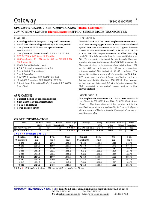
Optoway SPS-7350W-CXX0G**********************************************************************************************************************************************************************************************************************************************************************************************************************************************OPTOWAY TECHNOLOGY INC. No .38, Kuang Fu S. Road, Hu Kou, Hsin Chu Industrial Park, Hsin Chu, Taiwan 303Tel: 886-3-5979798 Fax: 886-3-59797371SPS-7350W-CXX0G / SPS-7350BW-CXX0G (RoHS Compliant)3.3V / CWDM / 1.25 Gbps Digital Diagnostic SFP LC SINGLE-MODE TRANSCEIVER **********************************************************************************************************************************************************************FEATURESl Hot-Pluggable SFP Footprint LC Optical Transceiver l Small Form-Factor Pluggable (SFP) MSA compatible l Compliant with IEEE 802.3z Gigabit Ethernet 1000BASE-XDl Compliant with Fibre Channel 1X SM-LC-L FC-PI l SFF-8472 Digital Diagnostic Functionl 18 Wavelength (λ): 1270 nm to 1610 nm CWDM DFB LD Transmitterl 19 dB Power Budget at Leastl AC/AC Coupling according to MSA l Single +3.3 V Power Supply l RoHS Compliantl 0 to 70o C Operation: SPS-7350W-CXX0G l -5 to 85o C Operation: SPS-7350BW-CXX0Gl Class 1 Laser International Safety Standard IEC-60825 CompliantAPPLICATIONSl Gigabit Ethernet Switches and Routers l Fibre Channel Switch Infrastructure l XDSL Applications l Metro Edge SwitchingDESCRIPTIONThe SPS-7350W-CXX0G series single mode transceivers is small form factor pluggable module for bi-directional serial optical data communications such as Gigabit Ethernet 1000BASE-XD and Fibre Channel 1x SM-LC-L FC-PI. It is with the SFP 20-pin connector to allow hot plug capability. Digital diagnostic functions are available via an I 2C. This module is designed for single mode fiber and operates at a nominal wavelength of CWDM wavelength. There are eighteen center wavelengths available from 1270 nm to 1610 nm, with each step 20 nm. A guaranteed minimum optical link budget of 19 dB is offered The transmitter section uses a multiple quantum well CWDM DFB laser and is a class 1 laser compliant according to International Safety Standard IEC-60825. The receiver section uses an integrated InGaAs detector preamplifier (IDP) mounted in an optical header and a limiting post-amplifier IC.LASER SAFETYThis single mode transceiver is a Class 1 laser product. It complies with IEC-60825 and FDA 21 CFR 1040.10 and 1040.11. The transceiver must be operated within the specified temperature and voltage limits. The optical ports of the module shall be terminated with an optical connector or with a dust plug.ORDER INFORMATIONP/No.Bit Rate (Gb/s) 1000 BASE Power Budget (dB) Wavelength (nm)Package Temp.(o C) TX Power (dBm) RX Sens. (dBm) RoHS Compliant SPS-7350W-CXX0G 1.25 XD > 19 CWDM * LC SFP with DMI 0 to 70 0 to -5 -24 Yes SPS-7350BW-CXX0G 1.25 XD > 19 CWDM * LC SFP with DMI -5 to 85 0 to -5 -24 YesCWDM * Wavelength (0 to 70o C)Central Wavelength Min. (nm) Typ. (nm)Max. (nm)Central WavelengthMin. (nm)Typ. (nm)Max. (nm)-C270 1264.5 1270 1277.5 -C450 1444.5 1450 1457.5 -C290 1284.5 1290 1297.5 -C470 1464.5 1470 1477.5 -C310 1304.5 1310 1317.5 -C490 1484.5 1490 1497.5 -C330 1324.5 1330 1337.5 -C510 1504.5 1510 1517.5 -C350 1344.5 1350 1357.5 -C530 1524.5 1530 1537.5 -C370 1364.5 1370 1377.5 -C550 1544.5 1550 1557.5 -C390 1384.5 1390 1397.5 -C570 1564.5 1570 1577.5 -C410 1404.5 1410 1417.5 -C590 1584.5 1590 1597.5 -C4301424.514301437.5-C6101604.516101617.5CWDM *: 18 Wavelengths from 1270 nm to 1610 nm, each step 20 nm.***********************************************************************************************************************************************************************OPTOWAY TECHNOLOGY INC. No .38, Kuang Fu S. Road, Hu Kou, Hsin Chu Industrial Park, Hsin Chu, Taiwan 303Absolute Maximum RatingsParameterSymbol Min Max Units NotesStorage TemperatureTstg -40 85 o COperating Case Temperature Topr 0 -5 70 85 o C SPS-7350W-CXX0G SPS-7350BW-CXX0G Power Supply VoltageVcc-0.53.6VRecommended Operating ConditionsParameterSymbol Min Typ Max Units / NotesPower Supply VoltageVcc 3.1 3.3 3.5 VOperating Case Temperature Topr 0 -5 70 85 oC / SPS-7350W-CXX0G oC / SPS-7350BW-CXX0GPower Supply Current I CC (TX+RX)200 300 mA Data Rate1001250Mb/sTransmitter Specifications (0o C < Topr < 70o C, 3.1V < Vcc < 3.5V)ParameterSymbol Min Typ Max Units NotesOpticalOptical Transmit Power Po -5 --- 0 dBm 1 Output Center Wavelength λ λc –5.5 λc λc +7.5 nm 2Output Spectrum Width∆λ --- --- 1 nm -20 dB Width Side Mode Suppression Ratio SMSR 30 dB Extinction Ratio E R 9 --- --- dBOptical Rise Time t r 260 ps 20 % to 80% Values Optical Fall Timet f 260 ps 20 % to 80% Values Relative Intensity Noise RIN -120 dB/HzElectricalData Input Current – Low I IL -350 µA Data Input Current – High I IH 350 µADifferential Input VoltageV IH - V IL 0.5 2.4 V Peak-to-PeakTX Disable Input Voltage – Low T DIS, L 0 0.5 V 3 TX Disable Input Voltage – High T DIS, H 2.0 Vcc V 3 TX Disable Assert Time T ASSERT 10 µs TX Disable Deassert TimeT DEASSERT 1 ms TX Fault Output Voltage -- Low T FaultL 0 0.5 V 4 TX Fault Output Voltage -- HighT FaultH2.0Vcc+0.3V41. Output power is power coupled into a 9/125 µm single mode fiber.2. ITU-T G.694.2 CWDM wavelength from 1270 nm to 1610 nm, each step 20 nm.3. There is an internal4.7K to 10K ohm pull-up resistor to VccTX.4. Open collector compatible, 4.7K to 10K ohm pull-up to Vcc (Host Supply Voltage).Receiver Specifications (0o C < Topr <70o C, 3.1V < Vcc < 3.5V)ParameterSymbol Min Typ Max Units NotesOptical SensitivitySens -24 dBm 4 Maximum Input Power Pin -3 dBm 4Signal Detect -- Asserted Pa --- -24 dBm Transition: low to high Signal Detect -- Deasserted Pd -36 --- --- dBm Transition: high to low Signal detect -- Hysteresis 1.0 --- dBWavelength of Operation 1100 --- 1620 nmElectricalDifferential Output VoltageV OH – V OL0.62.0V***********************************************************************************************************************************************************************OPTOWAY TECHNOLOGY INC. No .38, Kuang Fu S. Road, Hu Kou, Hsin Chu Industrial Park, Hsin Chu, Taiwan 303Output LOS Voltage -- Low V OL 0 0.5 V 5 Output LOS Voltage -- HighV OH2.0Vcc+0.3V54. Measured at 27-1 PRBS at BER 1E-12.5. Open collector compatible, 4.7K to 10K ohm pull-up to Vcc (Host Supply Voltage).Module DefinitionModule DefinitionMOD-DEF2 PIN 4 MOD-DEF1 PIN 5 MOD-DEF0 PIN 6 Interpretation by Host 4SDASCLLV-TTL LowSerial module definitionprotocolModule Definition 4 specifies a serial definition protocol. For this definition, upon power up, MOD-DEF(1:2) appear as no connector (NC) and MOD-DEF(0) is TTL LOW. When the host system detects this condition, it activates the serial protocol. The protocol uses the 2-wire serial CMOS E 2PROM protocol of the ATMEL AT24C01A/02/04 family of components.*********************************************************************************************************************************************************************** OPTOWAY TECHNOLOGY INC. No.38, Kuang Fu S. Road, Hu Kou, Hsin Chu Industrial Park, Hsin Chu, Taiwan 303。
XR17D158IV中文资料
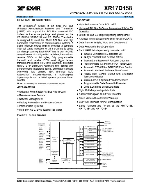
xr XR17D158UNIVERSAL (3.3V AND 5V) PCI BUS OCTAL UART NOVEMBER 2004REV. 1.2.1GENERAL DESCRIPTIONThe XR17D1581 (D158) is an octal PCI Bus Universal Asynchronous Receiver and Transmitter (UART) with support for PCI Bus universal VIO buffers in the same package and pin-out as the XR17C158, XR17C154 and XR17D154. The device is designed to meet the 32-bit PCI Bus and high bandwidth requirement in communication systems. A global interrupt source register provides a complete interrupt status indication for all 8 channels to speed up interrupt parsing. Each UART has its own 16C550 compatible set of configuration registers, transmit and receive FIFOs of 64 bytes, fully programmable transmit and receive FIFO level trigger levels, transmit and receive FIFO level counters, automatic RTS/CTS or DTR/DSR hardware flow control with programmable hysteresis levels, automatic software (Xon/Xoff) flow control, IrDA (Infrared Data Association) encoder/decoder, 8 multi-purpose inputs/outputs and a 16-bit general purpose timer/ counter.N OTE: 1 Covered by U.S. Patents #5,649,122 and #5,949,787 APPLICATIONS•Universal Form Factor PCI Bus Add-in Card •Remote Access Servers•Network Management•Factory Automation and Process Control•Point-of-Sale Systems•Multi-port RS-232/RS-422/RS-485 Cards FEATURES•High Performance Octal PCI UART•Universal PCI Bus Buffers - Auto-sense 3.3V or 5V Operation•32-bit PCI Bus 2.3 Target Signalling Compliance •A Global Interrupt Source Register for all 8 UARTs •Data Transfer in Byte, Word and Double-word •Data Read/Write Burst Operation•Each UART is independently controlled with:■16C550 Compatible 5G Register Set■64-byte Transmit and Receive FIFOs■Transmit and Receive FIFO Level Counters■Programmable TX and RX FIFO Trigger Level■Automatic RTS/CTS or DTR/DSR Flow Control■Automatic Xon/Xoff Software Flow Control■RS485 HDX Control Output with Selectable Turn-around Delay■Infrared (IrDA 1.0) Data Encoder/Decoder■Programmable Data Rate with Prescaler■Up to 6.25 Mbps Serial Data Rate•Eight Multi-Purpose Inputs/outputs•A General Purpose 16-bit Timer/counter•Sleep Mode with Automatic Wake-up •EEPROM Interface for PCI Configuration•Same Package and Pin-out as the XR17C158, XR17C154 and XR17D154F IGURE 1. B LOCK D IAGRAMExar Corporation 48720 Kato Road, Fremont CA, 94538 • (510) 668-7000 • FAX (510) 668-7017 • XR17D158xrUNIVERSAL (3.3V AND 5V) PCI BUS OCTAL UART REV. 1.2.12F IGURE 2. P IN O UT OF THE D EVICEORDERING INFORMATIONP ART N UMBER P ACKAGE O PERATING T EMPERATURE R ANGED EVICE S TATUSXR17D158CV 144-Lead TQFP 0°C to +70°C Active XR17D158IV144-Lead TQFP-40°C to +85°CActivexrXR17D158REV. 1.2.1UNIVERSAL (3.3V AND 5V) PCI BUS OCTAL UART3PIN DESCRIPTIONSN AMEP IN #T YPED ESCRIPTIONPCI LOCAL BUS INTERFACERST#134IPCI bus reset input (active low). It resets the PCI local bus configurationspace registers, device configuration registers and UART channel registers to the default condition.CLK 135I PCI bus clock input of up to 33.34MHz.AD31-AD25,AD24,AD23-AD16, AD15-AD8, AD7-AD0138-144,1,6-13,26-33,37-44IOAddress data lines [31:0] (bidirectional).FRAME#15I Bus transaction cycle frame (active low). It indicates the beginning and dura-tion of an access.C/BE0#-C/BE3#36,25,14,2IBus Command/Byte Enable [3:0] (active low). This line is multiplexed for bus Command during the address phase and Byte Enables during the data phase.IRDY#16IInitiator Ready (active low). During a write, it indicates that valid data ispresent on data bus. During a read, it indicates the master is ready to accept data.TRDY#17O Target Ready (active low).STOP#21O Target request to stop current transaction (active low). IDSEL 3I Initialization device select (active high). DEVSEL#18O Device select to the XR17D158 (active low).INTA#133OD Device interrupt from XR17D158 (open drain, active low).PAR 24IO Parity is even across AD[31:0] and C/BE[3:0]# (bidirectional, active high). PERR#22O Data Parity error indicator, except for Special Cycle transactions (active low). Optional in bus target application.SERR#23ODSystem error indicator, Address parity or Data parity during Special Cycle transactions (open drain, active low). Optional in bus target application.MODEM OR SERIAL I/O INTERFACETX0125O UART channel 0 Transmit Data or infrared transmit data. Normal TXD output idles HIGH while infrared TXD output idles LOW.RX0132IUART channel 0 Receive Data or infrared receive data. Normal RXD input idles HIGH. The infrared pulses typically idle LOW but can be inverted inter-nally prior the decoder by FCTR[4].RTS0#127O UART channel 0 Request to Send or general purpose output (active low).CTS0#131I UART channel 0 Clear to Send or general purpose input (active low).DTR0#126O UART channel 0 Data Terminal Ready or general purpose output (active low).DSR0#130I UART channel 0 Data Set Ready or general purpose input (active low).CD0#129IUART channel 0 Carrier Detect or general purpose input (active low).XR17D158xrUNIVERSAL (3.3V AND 5V) PCI BUS OCTAL UARTREV. 1.2.14RI0#128I UART channel 0 Ring Indicator or general purpose input (active low).TX1117O UART channel 1 Transmit Data or infrared transmit data. Normal TXD output idles HIGH while infrared TXD output idles LOW.RX1124IUART channel 1 Receive Data or infrared receive data. Normal RXD input idles HIGH. The infrared pulses typically idle LOW but can be inverted inter-nally prior the decoder by FCTR[4].RTS1#119O UART channel 1 Request to Send or general purpose output (active low).CTS1#123I UART channel 1 Clear to Send or general purpose input (active low).DTR1#118O UART channel 1 Data Terminal Ready or general purpose output (active low).DSR1#122I UART channel 1 Data Set Ready or general purpose input (active low).CD1#121I UART channel 1 Carrier Detect or general purpose input (active low).RI1#120I UART channel 1 Ring Indicator or general purpose input (active low).TX2106O UART channel 2 Transmit Data or infrared transmit data. Normal TXD output idles HIGH while infrared TXD output idles LOW.RX299IUART channel 2 Receive Data or infrared receive data. Normal RXD input idles HIGH. The infrared pulses typically idle LOW but can be inverted inter-nally prior the decoder by FCTR[4].RTS2#104O UART channel 2 Request to Send or general purpose output (active low).CTS2#100I UART channel 2 Clear to Send or general purpose input (active low).DTR2#105O UART channel 2 Data Terminal Ready or general purpose output (active low).DSR2#101I UART channel 2 Data Set Ready or general purpose input (active low).CD2#102I UART channel 2 Carrier Detect or general purpose input (active low).RI2#103I UART channel 2 Ring Indicator or general purpose input (active low).TX398O UART channel 3 Transmit Data or infrared transmit data. Normal TXD output idles HIGH while infrared TXD output idles LOW.RX391IUART channel 3 Receive Data or infrared receive data. Normal RXD input idles HIGH. The infrared pulses typically idle LOW but can be inverted inter-nally prior the decoder by FCTR[4].RTS3#96O UART channel 3 Request to Send or general purpose output (active low).CTS3#92I UART channel 3 Clear to Send or general purpose input (active low).d.DTR3#97O UART channel 3 Data Terminal Ready or general purpose output (active low).DSR3#93I UART channel 3 Data Set Ready or general purpose input (active low).CD3#94I UART channel 3 Carrier Detect or general purpose input (active low).RI3#95I UART channel 3 Ring Indicator or general purpose input (active low).TX488O UART channel 4 Transmit Data or infrared transmit data. Normal TXD output idles HIGH while infrared TXD output idles LOW.RX481IUART channel 4 Receive Data or infrared receive data. Normal RXD input idles HIGH. The infrared pulses typically idle LOW but can be inverted inter-nally prior the decoder by FCTR[4].PIN DESCRIPTIONSN AME P IN#T YPE D ESCRIPTIONxrXR17D158REV. 1.2.1UNIVERSAL (3.3V AND 5V) PCI BUS OCTAL UART5RTS4#86O UART channel 4 Request to Send or general purpose output (active low).CTS4#82I UART channel 4 Clear to Send or general purpose input (active low).DTR4#87O UART channel 4 Data Terminal Ready or general purpose output (active low).DSR4#83I UART channel 4 Data Set Ready or general purpose input (active low).CD4#84I UART channel 4 Carrier Detect or general purpose input (active low).RI4#85I UART channel 4 Ring Indicator or general purpose input (active low).TX580O UART channel 5 Transmit Data or infrared transmit data. Normal TXD output idles HIGH while infrared TXD output idles LOW.RX571IUART channel 5 Receive Data or infrared receive data. Normal RXD input idles HIGH. The infrared pulses typically idle LOW but can be inverted inter-nally prior the decoder by FCTR[4].RTS5#78O UART channel 5 Request to Send or general purpose output (active low).CTS5#72I UART channel 5 Clear to Send or general purpose input (active low).DTR5#79O UART channel 5 Data Terminal Ready or general purpose output (active low).DSR5#75I UART channel 5 Data Set Ready or general purpose input (active low).CD5#76I UART channel 5 Carrier Detect or general purpose input (active low).RI5#77I UART channel 5 Ring Indicator or general purpose input (active low).TX662O UART channel 6 Transmit Data or infrared transmit data. Normal TXD output idles HIGH while infrared TXD output idles LOW.RX655IUART channel 6 Receive Data or infrared receive data. Normal RXD input idles HIGH. The infrared pulses typically idle LOW but can be inverted inter-nally prior the decoder by FCTR[4].RTS6#60O UART channel 6 Request to Send or general purpose output (active low).CTS6#56I UART channel 6 Clear to Send or general purpose input (active low).DTR6#61O UART channel 6 Data Terminal Ready or general purpose output (active low).DSR6#57I UART channel 6 Data Set Ready or general purpose input (active low).CD6#58I UART channel 6 Carrier Detect or general purpose input (active low).RI6#59I UART channel 6 Ring Indicator or general purpose input (active low).TX754O UART channel 7 Transmit Data or infrared transmit data. Normal TXD output idles HIGH while infrared TXD output idles LOW.RX747IUART channel 7 Receive Data or infrared receive data. Normal RXD input idles HIGH. The infrared pulses typically idle LOW but can be inverted inter-nally prior the decoder by FCTR[4].RTS7#52O UART channel 7 Request to Send or general purpose output (active low).CTS7#48I UART channel 7 Clear to Send or general purpose input (active low).DTR7#53O UART channel 7 Data Terminal Ready or general purpose output (active low).DSR7#49IUART channel 7 Data Set Ready or general purpose input (active low).PIN DESCRIPTIONSN AME P IN#T YPE D ESCRIPTIONXR17D158xrUNIVERSAL (3.3V AND 5V) PCI BUS OCTAL UARTREV. 1.2.16CD7#50I UART channel 7 Carrier Detect or general purpose input (active low).RI7#51IUART channel 7 Ring Indicator or general purpose input (active low).ANCILLARY SIGNALSMPIO0108I/O Multi-purpose input/output 0. The function of this pin is defined thru the Con-figuration Register MPIOSEL, MPIOLVL, MPIOINV, MPIO3T and MPIOINT MPIO1107I/O Multi-purpose input/output 1. The function of this pin is defined thru the Con-figuration Register MPIOSEL, MPIOLVL, MPIOINV, MPIO3T and MPIOINT.MPIO274I/O Multi-purpose input/output 2. The function of this pin is defined thru the Con-figuration Register MPIOSEL, MPIOLVL, MPIOINV, MPIO3T and MPIOINT.MPIO373I/O Multi-purpose input/output 3. The function of this pin is defined thru the Con-figuration Register MPIOSEL, MPIOLVL, MPIOINV, MPIO3T and MPIOINT.MPIO468I/O Multi-purpose input/output 4. The function of this pin is defined thru the Con-figuration Register MPIOSEL, MPIOLVL, MPIOINV, MPIO3T and MPIOINT.MPIO567I/O Multi-purpose input/output 5. The function of this pin is defined thru the Con-figuration Register MPIOSEL, MPIOLVL, MPIOINV, MPIO3T and MPIOINT.MPIO666I/O Multi-purpose input/output 6. The function of this pin is defined thru the Con-figuration Register MPIOSEL, MPIOLVL, MPIOINV, MPIO3T and MPIOINT.MPIO765I/O Multi-purpose input/output 7. The function of this pin is defined thru the Con-figuration Register MPIOSEL, MPIOLVL, MPIOINV, MPIO3T and MPIOINT.EECK116OSerial clock to EEPROM. An internal clock of CLK divide by 256 is used for reading the vendor and sub-vendor ID during power up or reset. However, it can be manually clocked thru the Configuration Register REGB.EECS 115OChip select to a EEPROM device like 93C46. It is manually selectable thru the Configuration Register REGB. Requires a pull-up 4.7K ohm resistor for external sensing of EEPROM during power up. See DAN112 for further details.EEDI 114O Write data to EEPROM device. It is manually accessible thru the Configura-tion Register REGB.EEDO 113I Read data from EEPROM device. It is manually accessible thru the Configu-ration Register REGB.XTAL1110I Crystal or external clock input.XTAL2109O Crystal or buffered clock output. TMRCK 69I 16-bit timer/counter external clock input.ENIR70IInfrared mode enable (active high). This pin is sampled during power up, fol-lowing a hardware reset (RST#) or soft-reset (register RESET). It can be used to start up all 8 UARTs in the infrared mode. The sampled logic state is transferred to MCR bit-6 in the UART.TEST#111IFactory Test. Connect to VCC for normal operation.VCC64, 90,112Power supply for the UART core logic - 5V ONLY . This power supply deter-mines the VOH level of the non-PCI bus interface outputs. See Table 1 for valid combinations of VCC and VIO that can be used for the XR17D158.PIN DESCRIPTIONSN AME P IN #T YPE D ESCRIPTIONxrXR17D158REV. 1.2.1UNIVERSAL (3.3V AND 5V) PCI BUS OCTAL UART7N OTE : Pin type: I=Input, O=Output, IO= Input/output, OD=Output Open Drain.VIO4, 19, 34, 45,137PCI Bus I/O Power supply - 3.3V or 5V, detected by the auto-sense circuitry of the XR17D158. This power supply determines the VOH level of the PCI bus interface outputs.(PCI 2.3 signalling compliant at both 3.3V and 5V operation, suitable for uni-versal form factor add-in card application)GND5,20,35,46,63,89,136Power supply common, ground.PIN DESCRIPTIONSN AME P IN#T YPED ESCRIPTIONXR17D158xrUNIVERSAL (3.3V AND 5V) PCI BUS OCTAL UARTREV. 1.2.18FUNCTIONAL DESCRIPTIONThe XR17D158 (D158) integrates the functions of 8 enhanced 16550 UARTs with the PCI Local Bus interface and a non-volatile memory interface for PCI bus’s plug-and-play auto-configuration, a 16-bit timer/counter, 8 multi-purpose inputs/outputs, and an on-chip oscillator. The PCI local bus is a synchronous timing bus where all bus transactions are associated to the bus clock of up to 33MHz. The D158 supports 32-bit wide read and write data transfer operations including data burst mode through the PCI Local Bus interface. Read and write data operations may be in byte, word or double-word (DWORD) format. A single 32-bit interrupt status register provides interrupts status for all 8 UARTs, timer/counter, multipurpose inputs/outputs, and a special sleep wake up indicator. There are three sets of register in the device. First, the PCI local bus configuration registers for PCI auto configuration. A set of device configuration registers for overall control, 32-bit wide transmit and receive data transfer, and monitoring of the 8 UART channels. Lastly, each UART channel has its own 16550 UART compatible configuration register set for individual channel control, status, and byte wide data transfer.Each UART has 64-byte FIFOs, automatic RTS/CTS or DTR/DSR hardware flow control with hysteresis control, automatic Xon/Xoff and special character software flow control, programmable transmit and receive FIFO trigger level, FIFO level counters, infrared encoder and decoder (IrDA ver. 1.0), programmable baud rate generator with a prescaler of 1X or 4X, and data rate up to 6.25 Mbps at 8X sampling clock.The XR17D158 is available in a thin 144-pin TQFP (20x20x1.4mm) package in commercial and industrial temperature ranges.PCI L OCAL B US I NTERFACEThis is the host interface and it meets the PCI Local Bus Specification revision 2.3. The PCI local bus operations are synchronous meaning each transaction is associated to the bus clock. The XR17D158 can operate with the bus clock of up to a 33.34MHz. Data transfers operation can be formatted in 8-bit, 16-bit, 24-bit or 32-bit wide. With 32-bit data operations, it pushes the data transfer rate on the bus up to 132 MByte/sec. This increases the overall system’s communication performance up to 16 times better than the 8-bit ISA bus. See PCI local bus specification revision 2.3 for bus operation details.PCI L OCAL B US C ONFIGURATION S PACE R EGISTERSA set of PCI local bus configuration space register is provided. These registers provide the PCI local bus operating system with the card’s vendor ID, device ID, sub-vendor ID, product model number, and resources and capabilities. The PCI local bus operating system collects this data from all the cards on the bus during the auto configuration phase that follows immediately after a power up or system reset/reboot. After it has sorted out all devices on the bus, it defines and download the operating conditions to the cards. One of the definitions is the base address loaded into the Base Address Register (BAR) where the card will be operating in the PCI local bus memory space.EEPROM I NTERFACEAn external 93C46 EEPROM is only used to store the vendor’s ID and model number, and the sub-vendor’s ID and product model number. This information is only used with the plug-and-play auto configuration of the PCI local bus. These data provide automatic hardware installation onto the PCI bus. The EEPROM interface consists of 4 signals, EEDI, EEDO, EECS, and EECK. The EEPROM is not needed when auto configuration is not required in the application. However, If your design requires non-volatile memory for other purpose. It is possible to store and retrieve data on the EEPROM through a special PCI device configuration register. See application note DAN112 for its programming details.xr XR17D158 REV. 1.2.1UNIVERSAL (3.3V AND 5V) PCI BUS OCTAL UART 1.0APPLICATION EXAMPLESThe XR17D158 is designed to operate with VCC (voltage to the UART Core Logic) at 5V only, irrespective of whether the PCI bus is at 3.3V or 5V. Table 1 below shows the valid combinations of VCC and the PCI Bus Voltage, VIO that can be used for the device..T ABLE 1: V ALID C OMBINATIONS OF VCC AND VIO S UPPLY V OLTAGESVCC VIO5.0V 5.0V Valid5.0V 3.3V Valid3.3V 5.0V Invalid3.3V 3.3V InvalidA typical application for a universal add-in card (VCC must be 5V) is shown in Figure 3. In an embedded system, the designer must still choose 5V power supply for the VCC regardless of VIO (3.3 or 5V). In Figure 4, examples 1 and 2 show valid applications of the XR17D158 in an embedded system.F IGURE 3. T YPICAL A PPLICATION FOR A U NIVERSAL A DD-IN C ARD9XR17D158xrUNIVERSAL (3.3V AND 5V) PCI BUS OCTAL UART REV. 1.2.110F IGURE 4. T YPICAL A PPLICATIONS IN AN E MBEDDED S YSTEM2.0XR17D158 REGISTERSThe XR17D158 UART has three different sets of registers as shown in Figure 5. The PCI local bus configuration space registers are for plug-and-play auto-configuration when connecting the device to a the PCI bus. This auto-configuration feature makes installation very easy into a PCI system and it is part of the PCI local bus specification. The second register set is the device configuration registers that are accessible directly from the PCI bus for programming general operating conditions of the device and monitoring the status of various functions. These registers are mapped into 4K of the PCI bus memory address space. These functions include all 8 channel UART’s interrupt control and status, 16-bit general purpose timer control and status, multipurpose inputs/outputs control and status, sleep mode, soft-reset, and device identification and revision. And lastly, each UART channel has its own set of internal UART configuration registers for its own operation control and status reporting. All 8 sets of channel registers are embedded inside the device configuration registers space, which provides faster access. The following paragraphs describe all 3 sets of registers in detail.F IGURE 5. T HE XR17D158 R EGISTER S ETS2.1PCI LOCAL BUS CONFIGURATION SPACE REGISTERSThe PCI local bus configuration space registers are responsible for setting up the device’s operating environment in the PCI local bus. The pre-defined operating parameters of the device is read by the PCI bus plug-and-play auto-configuration manager in the operating system. After the PCI bus has collected all data from every device/card on the bus, it defines and downloads the memory mapping information to each device/ card about their individual operation memory address location and conditions. The operating memory mapped address location is downloaded into the Base Address Register (BAR) register, 0x10. The plug-and-play auto configuration feature is only available when an external 93C46 EEPROM is used. The EEPROM contains the device vendor and sub-vendor data required by the auto-configuration setup.UNIVERSAL (3.3V AND 5V) PCI BUS OCTAL UART REV. 1.2.1 T ABLE 2: PCI L OCAL B US C ONFIGURATION S PACE R EGISTERSA DDRESSB ITS T YPE D ESCRIPTION R ESET V ALUE(HEX)0x0031:16RWR1Device ID (Exar device ID number)0x0158 15:0RWR1Vendor ID (Exar) specified by PCISIG0x13A80x04313029:28RWCRWCROParity error detected. Cleared by writing a logic 1.System error detected. Cleared by writing a logic 1.Unused000027R-Reset Target Abort. Set whenever D158 terminates with a target abort. 026:25RO DEVSEL# timing. 0024RO Unemployments bus master error reporting bit023RO Fast back to back transactions are supported122:16RO Reserved Status bits000 000015:9,7,5,4,3,2RO Command bits (reserved)0x00008RWR SERR# driver enable. Logic 1=enable driver and 0=disabledriver0 6RWR Parity error enable. Logic 1=respond to parity error and 0=ignore01RWR Command controls a device’s response to mem space accesses:0=disable mem space accesses, 1=enable mem space accesses0RO Device’s response to I/O space accesses is disabled.(0 = disable I/O space accesses)0x0831:8RO Class Code (Simple 550 Communication Controller). 0x070002 7:0RO Revision ID (Exar device revision number) Current Rev. value 0x0C31:24RO BIST (Built-in Self Test)0x00 23:16RO Header Type (a single function device with one BAR) 0x0015:8RO Unimplemented Latency Timer (needed only for bus master)0x007:0RO Unimplemented Cache Line Size 0x000x1031:12RWR Memory Base Address Register (BAR)0x00 11:0RO Claims a 4K address space for the memory mapped UARTs0x0000x1431:0RO Unimplemented Base Address Register (returns zeros)0x000000000x18h31:0RO Unimplemented Base Address Register (returns zeros)0x000000000x1C31:0RO Unimplemented Base Address Register (returns zeros)0x000000000x2031:0RO Unimplemented Base Address Register (returns zeros)0x000000000x2431:0RO Unimplemented Base Address Register (returns zeros)0x000000000x2831:0RO Reserved 0x00000000N OTE : RWR 1=Read/Write from external EEPROM. RWR=Read/Write from AD[31:0]. RO= Read Only. RWC=Read/Write-Clear.2.2Device Configuration Register SetThe device configuration registers and a special way to access each of the UART’s transmit and receive data FIFOs are accessible directly from the PCI data bus. This provides easy programming of general operating parameters to the D158 UART and for monitoring the status of various functions. The registers occupy 4K of PCI bus memory address space. These addresses are offset onto the basic memory address, a value loaded into the Memory Base Address Register (BAR) in the PCI local bus configuration register set. These registers control or report on all 8 channel UARTs functions that include interrupt control and status, 16-bit general purpose timer control and status, multipurpose inputs/outputs control and status, sleep mode control, soft-reset control, and device identification and revision, and others.The registers set is mapped into 8 address blocks where each UART channel occupies 512 bytes memory space for its own 16550 compatible configuration registers. The device configuration and control registers are embedded inside the UART channel zero’s address space between 0x0080 to 0x0093. All these registers can be accessed in 8, 16, 24 or 32 bit width depending on the starting address given by the host at beginning of the bus cycle. Transmit and receive data may be loaded or unloaded in 8, 16, 24 or 32 bit format to the register’s address. Every time a read or write operation is made to the transmit or receive register, its FIFO data pointer is automatically bumped to the next sequential data location either in byte, word or dword. One special case applies to the receive data unloading when reading the receive data together with its LSR register content. The host must read them in 16 or 32 bits format in order to maintain integrity of the data byte with its associated error flags.0x2C31:16RWR 1Subsystem ID (write from external EEPROM by customer)0x000015:0RWR 1Subsystem Vendor ID (write from external EEPROM by cus-tomer)0x00000x3031:0RO Expansion ROM Base Address (Unimplemented)0x000000000x3431:0RO Reserved (returns zeros)0x000000000x3831:0RO Reserved (returns zeros)0x000000000x3C31:24RO Unimplemented MAXLAT 0x0023:16RO Unimplemented MINGNT 0x0015:8RO Interrupt Pin, use INTA#. 0x017:0RWRInterrupt Line.0xXXT ABLE 2: PCI L OCAL B US C ONFIGURATION S PACE R EGISTERSA DDRESSB ITS T YPE D ESCRIPTIONR ESET V ALUE(HEX )UNIVERSAL (3.3V AND 5V) PCI BUS OCTAL UART REV. 1.2.1T ABLE 3: XR17D158 D EVICE C ONFIGURATION R EGISTERSO FFSET A DDRESS M EMORY S PACE R EAD/W RITE D ATA W IDTH C OMMENT0x000 - 0x00F UART channel 0 Regs (Table 12 & Table 13)8/16/24/32First 8 regs are 16550 compatible0x010 - 0x07F Reserved0x080 - 0x093DEVICE CONFIG.(Table 4)8/16/24/32REGISTERS0x094 - 0x0FF Reserved0x100 - 0x13F UART 0 – Read FIFO Read-Only8/16/24/3264 bytes of RX FIFO data0x100 - 0x13F UART 0 – Write FIFO Write-Only8/16/24/3264 bytes of TX FIFO data0x140 - 0x17F ReservedRead-Only16/3264 bytes of RX FIFO data + LSR0x180 - 0x1FF UART 0 – Read FIFOwith errors0x200 - 0x20F UART channel 1 Regs (Table 12 & Table 13)8/16//24/32First 8 regs are 16550 compatible0x210 - 0x2FF Reserved0x300 - 0x33F UART 1 – Read FIFO Read-Only8/16/24/3264 bytes of RX FIFO data0x300 - 0x33F UART 1 – Write FIFO Write-Only8/16/24/3264 bytes of TX FIFO data0x340 - 0x37F Reserved0x380 - 0x3FF UART 1 – Read FIFORead-Only16/3264 bytes of RX FIFO data + LSR with errors0x400 - 0x40F UART channel 2 Regs (Table 12 & Table 13)8/16/24/32First 8 regs are 16550 compatible0x410 - 0x4FF Reserved0x500 - 0x53F UART 2 – Read FIFO Read-Only8/16/24/3264 bytes of RX FIFO data0x500 - 0x53F UART 2 – Write FIFO Write-Only8/16/24/3264 bytes of TX FIFO data0x540 - 0x57F ReservedRead-Only16/3264 bytes of RX FIFO data + LSR0x580 - 0x5FF UART 2 – Read FIFOwith errors0x600 - 0x60F UART channel 3 Regs (Table 12 & Table 13)8/16/24/32First 8 regs are 16550 compatible0x610 - 0x6FF Reserved0x700 - 0x73F UART 3 – Read FIFO Read-Only8/16/24/3264 bytes of RX FIFO data0x700 - 0x73F UART 3 – Write FIFO Write-Only8/16/24/3264 bytes of TX FIFO data0x740 - 0x77F ReservedRead-Only16/3264 bytes of RX FIFO data + LSR0x780 - 0x7FF UART 3 – Read FIFOwith errors。
欧洲品牌电磁器件型号123456产品说明书
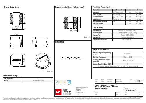
Dimensions: [mm]Scale - 5:174404054047BC74404054047T e m p e r a t u r eT pT L74404054047Cautions and Warnings:The following conditions apply to all goods within the product series of WE-LQS of Würth Elektronik eiSos GmbH & Co. KG:General:•This electronic component is designed and manufactured for use in general electronic equipment.•Würth Elektronik must be asked for written approval (following the PPAP procedure) before incorporating the components into any equipment in fields such as military, aerospace, aviation, nuclear control, submarine, transportation (automotive control, train control, ship control), transportation signal, disaster prevention, medical, public information network etc. where higher safety and reliability are especially required and/or if there is the possibility of direct damage or human injury.•Electronic components that will be used in safety-critical or high-reliability applications, should be pre-evaluated by the customer. •The component is designed and manufactured to be used within the datasheet specified values. If the usage and operation conditions specified in the datasheet are not met, the wire insulation may be damaged or dissolved.•Do not drop or impact the components, the component may be damaged.•Würth Elektronik products are qualified according to international standards, which are listed in each product reliability report. Würth Elektronik does not warrant any customer qualified product characteristics beyond Würth Elektroniks’ specifications, for its validity and sustainability over time.•The responsibility for the applicability of the customer specific products and use in a particular customer design is always within the authority of the customer. All technical specifications for standard products also apply to customer specific products.Product specific:Soldering:•The solder profile must comply with the technical product specifications. All other profiles will void the warranty.•All other soldering methods are at the customers’ own risk.•Strong forces which may affect the coplanarity of the components’ electrical connection with the PCB (i.e. pins), can damage the part, resulting in avoid of the warranty.Cleaning and Washing:•Washing agents used during the production to clean the customer application might damage or change the characteristics of the wire insulation, marking or plating. Washing agents may have a negative effect on the long-term functionality of the product.•Using a brush during the cleaning process may break the wire due to its small diameter. Therefore, we do not recommend using a brush during the PCB cleaning process.Potting:•If the product is potted in the customer application, the potting material may shrink or expand during and after hardening. Shrinking could lead to an incomplete seal, allowing contaminants into the core. Expansion could damage the components. We recommend a manual inspection after potting to avoid these effects.Storage Conditions:• A storage of Würth Elektronik products for longer than 12 months is not recommended. Within other effects, the terminals may suffer degradation, resulting in bad solderability. Therefore, all products shall be used within the period of 12 months based on the day of shipment.•Do not expose the components to direct sunlight.•The storage conditions in the original packaging are defined according to DIN EN 61760-2.•The storage conditions stated in the original packaging apply to the storage time and not to the transportation time of the components. Packaging:•The packaging specifications apply only to purchase orders comprising whole packaging units. If the ordered quantity exceeds or is lower than the specified packaging unit, packaging in accordance with the packaging specifications cannot be ensured. Handling:•Violation of the technical product specifications such as exceeding the nominal rated current will void the warranty.•Applying currents with audio-frequency signals may result in audible noise due to the magnetostrictive material properties.•The temperature rise of the component must be taken into consideration. The operating temperature is comprised of ambient temperature and temperature rise of the component.The operating temperature of the component shall not exceed the maximum temperature specified.These cautions and warnings comply with the state of the scientific and technical knowledge and are believed to be accurate and reliable.However, no responsibility is assumed for inaccuracies or incompleteness.Würth Elektronik eiSos GmbH & Co. KGEMC & Inductive SolutionsMax-Eyth-Str. 174638 WaldenburgGermanyCHECKED REVISION DATE (YYYY-MM-DD)GENERAL TOLERANCE PROJECTIONMETHODChrB.001.0062022-10-01DIN ISO 2768-1mDESCRIPTIONWE-LQS SMT Semi-ShieldedPower Inductor ORDER CODE74404054047SIZE/TYPE BUSINESS UNIT STATUS PAGEImportant NotesThe following conditions apply to all goods within the product range of Würth Elektronik eiSos GmbH & Co. KG:1. General Customer ResponsibilitySome goods within the product range of Würth Elektronik eiSos GmbH & Co. KG contain statements regarding general suitability for certain application areas. These statements about suitability are based on our knowledge and experience of typical requirements concerning the areas, serve as general guidance and cannot be estimated as binding statements about the suitability for a customer application. The responsibility for the applicability and use in a particular customer design is always solely within the authority of the customer. Due to this fact it is up to the customer to evaluate, where appropriate to investigate and decide whether the device with the specific product characteristics described in the product specification is valid and suitable for the respective customer application or not.2. Customer Responsibility related to Specific, in particular Safety-Relevant ApplicationsIt has to be clearly pointed out that the possibility of a malfunction of electronic components or failure before the end of the usual lifetime cannot be completely eliminated in the current state of the art, even if the products are operated within the range of the specifications.In certain customer applications requiring a very high level of safety and especially in customer applications in which the malfunction or failure of an electronic component could endanger human life or health it must be ensured by most advanced technological aid of suitable design of the customer application that no injury or damage is caused to third parties in the event of malfunction or failure of an electronic component. Therefore, customer is cautioned to verify that data sheets are current before placing orders. The current data sheets can be downloaded at .3. Best Care and AttentionAny product-specific notes, cautions and warnings must be strictly observed. Any disregard will result in the loss of warranty.4. Customer Support for Product SpecificationsSome products within the product range may contain substances which are subject to restrictions in certain jurisdictions in order to serve specific technical requirements. Necessary information is available on request. In this case the field sales engineer or the internal sales person in charge should be contacted who will be happy to support in this matter.5. Product R&DDue to constant product improvement product specifications may change from time to time. As a standard reporting procedure of the Product Change Notification (PCN) according to the JEDEC-Standard inform about minor and major changes. In case of further queries regarding the PCN, the field sales engineer or the internal sales person in charge should be contacted. The basic responsibility of the customer as per Section 1 and 2 remains unaffected.6. Product Life CycleDue to technical progress and economical evaluation we also reserve the right to discontinue production and delivery of products. As a standard reporting procedure of the Product Termination Notification (PTN) according to the JEDEC-Standard we will inform at an early stage about inevitable product discontinuance. According to this we cannot guarantee that all products within our product range will always be available. Therefore it needs to be verified with the field sales engineer or the internal sales person in charge about the current product availability expectancy before or when the product for application design-in disposal is considered. The approach named above does not apply in the case of individual agreements deviating from the foregoing for customer-specific products.7. Property RightsAll the rights for contractual products produced by Würth Elektronik eiSos GmbH & Co. KG on the basis of ideas, development contracts as well as models or templates that are subject to copyright, patent or commercial protection supplied to the customer will remain with Würth Elektronik eiSos GmbH & Co. KG. Würth Elektronik eiSos GmbH & Co. KG does not warrant or represent that any license, either expressed or implied, is granted under any patent right, copyright, mask work right, or other intellectual property right relating to any combination, application, or process in which Würth Elektronik eiSos GmbH & Co. KG components or services are used.8. General Terms and ConditionsUnless otherwise agreed in individual contracts, all orders are subject to the current version of the “General Terms and Conditions of Würth Elektronik eiSos Group”, last version available at .Würth Elektronik eiSos GmbH & Co. KGEMC & Inductive SolutionsMax-Eyth-Str. 174638 WaldenburgGermanyCHECKED REVISION DATE (YYYY-MM-DD)GENERAL TOLERANCE PROJECTIONMETHODChrB.001.0062022-10-01DIN ISO 2768-1mDESCRIPTIONWE-LQS SMT Semi-ShieldedPower Inductor ORDER CODE74404054047SIZE/TYPE BUSINESS UNIT STATUS PAGE。
ST735SCD,ST735SCD, 规格书,Datasheet 资料
1/11October 2002sCONVERTS +4.0V TO +6.2V INPUT TO -5V OUTPUT (735S)OR +3.5V TO +9.0V TO A NEGATIVE ADJUSTABLE OUTPUT (735T)s 1W GUARANTEED OUTPUT POWER s 72%TYPICAL EFFICIENCY s 0.8mA QUIESCENT CURRENT s 1µA SHUTDOWN MODEs 300KHZ FIXED FREQUENCY OSCILLATOR s CURRENT MODE PWM CONVERTER s LOW NOISE AND JITTER s SOFT STARTs SIMPLE APPLICATION CIRCUIT sUNDERVOLTAGE LOCKOUT (735S)DESCRIPTIONThe ST735S/ST735T is a Bi-CMOS,inverting switch mode DC-DC regulator with internal Power MOSFET that generates a fixed -5V (S version)or a negative adjustable (T version)output voltage from a 4V (3.5V for the 735T)to 6.2V input voltage (9V for the 735T);is guaranteed an output current of 200mA for inputs greater than 4.5V.The quiescent current for this device is typically of 0.8mA and,in shutdown mode it is reduced to1µA.These power-conserving features,along with high efficiency and applications circuits,thaT lend itself to minaturization,make the ST735S/ST735T excellent in a broad range of on-card,HDD and portable equipment applications.These device employ a high performance current mode pulse with modulation (PWM)control scheme to provide tight output voltage regulation and low noise.The fixed frequency oscillator is factory trimmed to 300KHz,allowing for easy noise filtering.The regulator in production is tested to guarantee an output accuracy within ±5%over all specified conditions.ST735S ST735T300kHz,-5V/ADJ INVERTING,NEGATIVE OUTPUTCURRENT-MODE PWMREGULATORl c -O bs o e t eP r od u t (sl c )Ob so e t et eP r od u t (sST735S/ST735T2/11ABSOLUTE MAXIMUM RATINGSAbsolute Maximum Ratings are those values beyond which damage to the device may occur.Functional operation under these condition is not implied.Note 1:The input to output differential voltage is limited to V IN +|V OUT |<12.7VTHERMAL DATACONNECTION DIAGRAM (top view)PIN DESCRIPTIONSymbol ParameterValue Unit V IN DC Input Voltage (V IN to GND)for ST735S -0.3to +7V V IN DC Input Voltage (V IN to GND)for ST735T (Note 1)-0.3to +11V SHDN Shutdown Voltage (SHDN to GND)-0.3to V IN +0.3V V LX Switch Voltage (Lx to V IN )-12.5to +0.3V V FB Feedback Voltage (V OUT to GND)-11to +0.3V V OUT Output Voltage (V OUT to GND)-11to +0.3V Other Input Voltage (SS,CC to GND)-0.3to V ++0.3V I LX Peack Switch Current 2A P tot Power Dissipation at T j =70°C DIP-8725mW SO-8470T stg Storage Temperature Range-55to +150°CT opOperating Junction Temperature Range-40to +125°CSymbol ParameterDIP-8SO-8Unit R thj-caseThermal Resistance Junction-case28°C/WPin N°Symbol Name and Function1SHDN SHUT-DOWN Control (V CC =ON GND=Shutdown2V REF Reference Output Voltage 3SSSoft Start4CC Compensation Input 5V OUT Negative Output Voltage6GND Ground7LX Switch Output8V INPositive Supply -Voltage Inputl s Ob so e t ePr od u c t () -O bST735S/ST735T3/11ORDERING CODESTYPICAL APPLICATION CIRCUITNOTE:1)All capacitors are X7R ceramic2)C 5can be omitted if are used higher values for the input and output capacitors (suggested C 2=47µF,C 1=100µF).3)R 1and R 2must be placed is ST735T applications only.Their values are calculated by the following formula R 2=(|V OUT |/V REF )xR 1.For R 1can be chosen any value between 2k Ωand 20k ΩAPPLICATION CIRCUITTo achieve the best performances from switching power supply topology,particular care to layout drawing is needed,in order to minimize EMI and obtain low noise.Moreover,jitter free operation ensures the full device yout design proposed on demoboard helps to lower the developing time.Wire lengths must be minimized,filter and bypass capacitors must be low ESRtype,placed as close as possible to the integrated circuit.The 4.7µF (or 6.8µF)inductor must be chosen built on a core,taking care that saturation current should be higher than the peak LX switch current.See the Peak Inductor Current vs Output Current graph.PRINTED DEMOBOARD (not in scale)TYPE DIP-8SO-8SO-8(T&R)ST735S ST735SCN ST735SCD ST735SCD-TR ST735TST735TCNST735TCDST735TCD-TRl t l u )Ob so e t ePr od u c (s )- O bs o e t eP r od c t(sST735S/ST735T4/11ELECTRICAL CHARACTERISTICS OF ST735S (Refer to test circuit,V IN =5V,C IN =4.7µF,C OUT =10µF all X7R ceramic,L =4.7µH (Note1),I OUT =0mA,T amb =-40to 125°C,unless otherwise specified.Typical value are referred at T amb =25°C)Note 1:Utilize of 6.8µH permits to reach higher current capability at the same operating conditions Note2:Guaranteed by design,but not tested in production Note3:Tested at I VREF =125µASymbol ParameterTest ConditionsMin.Typ.Max.Unit V IN Input Voltage 4 6.2V V OUTOutput VoltageV IN =4.5V to 6.2V I OUT =0to 200mA T amb =-40to 125°C-5.25-5-4.75V V IN =4.0V to 6.2V I OUT =0to 175mA T amb =-40to 125°C-5.25-5-4.75V I OUTOutput CurrentV IN =4.5V to 6.2V T J =0to 125°C 200275mA V IN =4.5V to 6.2V I OUT =0to 175mA T amb =-40to 125°C 175mA V IN =4.0VV OUT =-5V175mAI SUPPLY Supply Current Includes Switch Current0.8 1.6mAI STANDBY Standby CurrentV SHDN =0V 110µA I SC Short Circuit Current V IN =5V 0.9A I PEAK LX Max Peak Current (Note 2)1.5A V LO Undervoltage Lock-out 3.54V ∆V OUT Line Regulation V IN =4.0V to 6.2V 0.1%/V ∆V OUT Load Regulation I OUT =0to 200mA 0.003%/mA V REF Reference Voltage T amb =25°C (Note 3) 1.225V ∆V REF Reference Drift T amb =-40to 125°C50ppm/°C R DSON LX ON Voltage 0.5ΩI LEAK LX Leakage Current V DS =10V 1µAI SH Shutdown Pin Current 1µA V IL Shutdown Input Low Threshold0.25V V IH Shutdown Input High Threshold2Vf OSC Maximum Oscillator Frequency 300KHz νEfficencyI OUT =100mA72%R CCCompensation Pin Impedance on CC Pin7.5K Ωl t l u )Ob so e t ePr od u c (s )- O bs o e t eP r od c t(sST735S/ST735T5/11ELECTRICAL CHARACTERISTICS OF ST735T (Refer to test circuit,V IN =5V,C IN =4.7µF,C OUT =10µF all X7R ceramic,L =4.7µH (Note1),I OUT =0mA,V O adjusted to -5V,T amb =-40to 125°C,unless otherwise specified.Typical value are referred at Tamb=25°C)Note 1:Utilize of 6.8µH permits to reach higher current capability at the same operating conditions Note2:Guaranteed by design,but not tested in production Note3:Tested at I VREF =125µASymbol ParameterTest ConditionsMin.Typ.Max.Unit V IN Input Voltage 3.59V V OOutput VoltageV IN =4.5V to 6.2V I OUT =0to 200mA T amb =-40to 125°C-5.25-5-4.75V V IN =4.0V to 6.2V I OUT =0to 175mA T amb =-40to 125°C-5.25-5-4.75V I OOutput CurrentV IN =4.5V to 6.2V T amb =0to 125°C 200275mA V IN =4.5V to 6.2V I OUT =0to 175mA T amb =-40to 125°C 175mA V IN =4.0VV OUT =-5V175mAI SUPPLY Supply Current Includes Switch Current0.8 1.6mAI STANDBY Standby CurrentV SHDN =0V 110µA I SC Short Circuit Current V IN =5V 0.9A I PEAK LX Max Peak Current (Note 2)1.5A V LO Undervoltage Lock-out 3.54V ∆V OUT Line Regulation V IN =4.0V to 6.2V 0.1%/V ∆V OUT Load Regulation I OUT =0to 200mA 0.003%/mA V REF Reference Voltage T amb =25°C (Note 3) 1.225V ∆V REF Reference Drift T amb =-40to 125°C50ppm/°C R DSON LX ON Voltage 0.5ΩI LEAK LX Leakage Current V DS =10V 1µAI SH Shutdown Pin Current 1µA V IL Shutdown Input Low Threshold0.25V V IH Shutdown Input High Threshold2Vf OSC Maximum Oscillator Frequency 300KHz νEfficencyI OUT =100mA72%R CCCompensation Pin Impedance on CC Pin7.5K ΩO-O ST735S/ST735T6/11TYPICAL CHARACTERISTICS (Referred to typical application circuit,T amb =25°C unless otherwise specified)Figure 1:Output Voltage vs TemperatureFigure 2:Reference Voltage vs Temperature Figure 3:Efficency vs TemperatureFigure 4:Efficency vs Ouput CurrentFigure 5:Efficency vs Low Ouput CurrentFigure 6:Supply Current vs TemperatureOo-OsST735S/ST735T7/11Figure7:Supply Current vs Input Voltage for ST735SFigure8:Supply Current vs Input Voltage for ST734TFigure9:Shutdown Threshold vs Temperature Figure10:Peack Inductor vs Output Current Figure11:Switch Current Limit vs Soft Start VoltageFigure12:Oscillator Frequency Vs Temperaturel l c )Ob so e t ePr o-O bs o e t eP r od u t (sST735S/ST735T8/11Figure 13:LX On Resistance vs TemperatureFigure 14:LX On Resistance vs Input Voltage Figure 15:Load TransientFigure 16:Load TransientFigure 17:Load TransientFigure 18:Switching WaveformV I =5V,I O =20mA to 200mA,C I =4.7µF,C O =100µF,t r =t f =1µs V I =5V,I O =20mA to 200mA,C I =4.7µF,C O =100µF,t f =1µsV I =5V,I O =20mA to 200mA,C I =4.7µF,C O =100µF,t r =1µsV I =5V,I O =100mAl slc)O b s oe t eP ro du ct()-O bs oe t eP ro dut(sST735S/ST735T11/11Information furnished is believed to be accurate and reliable. However, STMicroelectronics assumes no responsibility for the consequences of use of such information nor for any infringement of patents or other rights of third parties which may result from its use. No license is granted by implication or otherwise under any patent or patent rights of STMicroelectronics. Specifications mentioned in this publication are subject to change without notice. This publication supersedes and replaces all information previously supplied. STMicroelectronics products are not authorized for use as critical components in life support devices or systems without express written approval of STMicroelectronics.© The ST logo is a registered trademark of STMicroelectronics© 2002 STMicroelectronics - Printed in Italy - All Rights ReservedSTMicroelectronics GROUP OF COMPANIESAustralia - Brazil - Canada - China - Finland - France - Germany - Hong Kong - India - Israel - Italy - Japan - Malaysia - Malta - Morocco Singapore - Spain - Sweden - Switzerland - United Kingdom - United States.© 芯天下--/。
Advance Adapter AX15传动适配器书 Насе代码712563说明书

SPECIAL NOTE: The components packaged in this kit have been assembled and machined for specific type of conversions. Modifications to any of the components will void any possible warranty or return privileges. If you do not fully understand modifications or changes that will be required to complete your KIT CONSITS OF:No: Qty Part No.DescriptionOPTIONAL ITEMS:PAGE 1 OF 3 Page Rev. Date: 03-22-17P/N: 712563AX15 TRANSMISSION RETRO-FITFOR THE AX5 4 CYL. 5 SPEED EXT. SLAVE1. 1 712563-PLT AX15 ADAPTER PLATE2. 1 712563-RET T/O BEARING SNOUT3. 1 712590-C T/O BEARING ASSY .4. 4 715523-SP CROSSMEMBER SPACERS5. 2 716086 AX5 BELLHOUSING DOWEL PIN6. 1 716167 .750 PILOT BUSHING (AX15 1995 & Newer)7. 1 716742 AX15 SEAL8. 4 724328 7/16-14 x 1-1/4" H.H.C.S. (Crossmember)9. 2 720039 10mm-1.25 x 20mm S.H.C.S(bell by slave cyl)10. 13 720091 10mm-1.25 x 24mm S.H.C.S.11. 2 7200928mm-1.25 x 24mm S.H.C.S.12. 4 723103 LOCK WASHER (Retainer)13. 4 723113 5/16"-18 x 7/8" S.H.C.S. (Retainer)14.13838241-1/8" 10 SPLINE DISC (CF382438)INSTALLATION NOTES:This kit is designed to fit the 1995 and newer AX15 transmission. Earlier model transmissions can use a stock pilot bushing, one with a .590" I.D. We recommend that the stock flywheel be removed and resurfaced at a machine shop. A new clutch disc and release bearing has been provided in this kit. A new pressure plate is also recommended before installing your new transmission. We offer a Centerforce pressure plate, Part No. CF361914.Before disposing of the old AX5 transmission, you will need to retain the shifter housing from that transmission. You will also be using the stock 4 cylinder bellhousing and stock release arm and crossmember mount.The transfer case must have a new input gear installed to fit to the AX15 transmission. If retaining the NP231 transfer case and because the new transmission is longer, we highly recommend a fixed yoke kit to be installed during this transmission swap. This will allow for a new, longer rear drive shaft. The Atlas 2 speed or 4 speed transfer cases are also an excellent upgrade to your Jeep, and this would be the perfect time for this additional upgrade.ASSEMBLY PROCEDURES:1. Refer to a service manual for the removal of the stock AX5 transmission. Also remove the pressure plate, disc, andflywheel.2. Resurface the flywheel and remove the old pilot bushing. Check the new pilot bushing on the AX15 pilot tip andThe AX5 transmission was coupled to a 21 spline transfer case. The AX15 transmission has a 23 output shaft. When upgrading your transmission, you will also be required to change out the input gear of the transfer case.716054 1987-1994 NP231 T/Cs 716095 1995-2006 NP231 T/Cs 716096 NP207 T/CsThe transfer case shifter braket must also be changed.Jeep YJs P/N 715545Jeep TJs P/N 715542AX15 shifter spacer, needed if you are using a rebuilt trans that does not have a shifter supplied with the transmission. allows the AX5 shifter to be used. P/N 712563-S & (4) 720066PAGE 2 OF 3 Page Rev. Date: 03-22-17P/N: 712563SPECIAL NOTE: The components packaged in this kit have been assembled and machined for specific type of conversions. Modifications to any of the components will void any possible warranty or return privileges. If you do not fully understand modifications or changes that will be required to complete your AX15 TRANSMISSION RETRO-FITFOR THE AX5 4 CYL. 5 SPEED EXT. SLAVEinstall into flywheel if it is the correct size. Mount the flywheel to the block and torque the flywheel bolts to factory specifications.3. Install the new clutch disc and pressure plate onto the flywheel4. Install the two new dowel pins into the adapter plate. The pins are a press fit.5. With the AX15 transmission on a work bench, remove the front bearing retainer. Clean the surface of any silicone.6.Apply a new thin film of silicon to the transmission face where the front retainer was just removed. Install the new adapter plate to the transmission. This adapter aligns to the front input bearing of the AX15 transmission. We have provided two clearance pockets on the adapter plate for the old AX15 dowel pins. Install the six 10mm bolts and the two 8mm bolts to retain the adapter plate.7. Install the new seal into the new retainer snout. Then install the retainer onto the adapter plate with silicone around the outside edge to seal the retaier to the plate. 8.The stock 4 cylinder bellhousing should now be installed onto the adapter plate. Make sure the new dowel pins in the plate align to the bellhousing. Install the new release bearing onto the stock release arm. Install these components into the bell -housing. Check for slave cylinder clearance on the adapter plate and bellhousing.9.Most rebuilt A X15 transmissions come with a shift handle. If yours did not, then you will need our P/N 712563-S and proceed with this step. The AX5 shifter bolts to the transmission with four bolts and this is a different bolt pattern than that of the AX15transmission. Since a new shift handle may be hard to come by, we have opted tomake the AX5 shifter work with the AX15 transmission. The shift body bolt holes are approximately a 1/2" of a hole off from bolting on to the AX15 transmission.So remove the stick from the aluminum shift housing and elongate the four holes to line up with the AX15 transmission hole, using 712563-S as a template. Once the holes line up with the AX15, you will also be required to modify the oil splash sheet metal piece. The new modified shifter can then be installed onto the AX15 transmission. Silicone should be applied on each surface. The 712563-S goes on first, the sheet metal oil shield second, and the aluminum housing last. Note the last two pieces are installed backward compared to how they were removed from the AX5 transmission. Once the transmission gets installed into the Jeep, the handle needs to be reinstalled.4320 Aerotech Center WayPaso Robles, CA 93447Telephone: (800) 350-2223 Fax: (805) 238-4201PAGE 3 OF 3 Page Rev. Date: 03-22-17P/N: 71256310. Install the transmission into the Jeep and reconnect the starter flywheel sensor and hydraulics.11. Install the new input gear to your transfer case and install the transfer case to the new transmission. The transfer caseshift bracket is normally installed through two of the bolt holes for the transfer case, so the new bracket should also be installed.12. The crossmember mount can be retained with a few modifications. The AX15 crossmember mount is approximately2" further back than the AX5 transmission. The bolt pattern is also different. The AX15 has a square pattern different than that of the AX5. The rubber support on the crossmember is the same square pattern as the AX15 transmission.By unbolting the rubber support, you can use it as a template for the new holes that need to be drilled 1-3/4" to 2"rearward on the mount. We found that it was easier to slot the steel mount side-to-side to allow for some adjustment once installed into the vehicle. The front portion of the steel mount should be cut off as not to interfere with the new transmission. We have included 4 spacer that get installed between the transmission and the steel mount to aid in clearance. Once the mount is modified. reattach the rubber mount and install onto the transmission. The rubber mount has four bolts that protrude from it. They should line up with the slots in the skid pan.13. The handle needs to be reinstalled into the top of the AX15 transmission.14. Drivelines need to be measured and modified.SPECIAL NOTE: The components packaged in this kit have been assembled and machined for specific type of conversions. Modifications to any of the components will void any possible warranty or return privileges. If you do not fully understand modifications or changes that will be required to complete your AX15 TRANSMISSION RETRO-FIT FOR THE AX5 4 CYL. 5 SPEED EXT. SLAVE。
AO4459中文资料

AO4459中⽂资料SymbolTyp Max 33406275R θJL 1824Maximum Junction-to-Lead CSteady-State°C/WThermal Characteristics ParameterUnits Maximum Junction-to-AmbientAt ≤ 10s R θJA °C/W Maximum Junction-to-Ambient ASteady-State °C/W AO4459AO4459SymbolMin TypMaxUnits BV DSS -30V -1T J =55°C-5I GSS ±100nA V GS(th)-1.5-1.85-2.5V I D(ON)-30A 3846T J =125°C53685872m ?g FS 11S V SD -0.78-1V I S-3.5A C iss 668830pF C oss 126pF C rss 92pF R g69?Q g (10V)12.716nC Q g (4.5V) 6.4nC Q gs 2nC Q gd 4nC t D(on)7.7ns t r 6.8ns t D(off)20ns t f 10ns t rr 2230ns Q rr15nCTHIS PRODUCT HAS BEEN DESIGNED AND QUALIFIED FOR THE CONSUMER MARKET. APPLICATIONS OR USES AS CRITICAL COMPONENTS IN LIFE SUPPORT DEVICES OR SYSTEMS ARE NOT AUTHORIZED. AOS DOES NOT ASSUME ANY LIABILITY ARISING OUT OF SUCH APPLICATIONS OR USES OF ITS PRODUCTS. AOS RESERVES THE RIGHT TO IMPROVE PRODUCT DESIGN,FUNCTIONS AND RELIABILITY WITHOUT NOTICE.DYNAMIC PARAMETERS Maximum Body-Diode Continuous CurrentGate resistanceV GS =0V, V DS =0V, f=1MHzV GS =0V, V DS =-15V, f=1MHz Input Capacitance Output Capacitance Turn-On Rise Time Turn-Off DelayTime V GS =-10V, V DS =-15V, R L =2.5?, R GEN =3?Turn-Off Fall TimeTurn-On DelayTime SWITCHING PARAMETERSTotal Gate Charge (4.5V)Gate Source Charge Gate Drain Charge Total Gate Charge (10V)V GS =-10V, V DS =-15V, I D =-6.5Am ?V GS =-4.5V, I D =-5AI S =-1A,V GS =0V V DS =-5V, I D =-6.5AR DS(ON)Static Drain-Source On-ResistanceForward TransconductanceDiode Forward VoltageI DSS µA Gate Threshold Voltage V DS =V GS I D =-250µA V DS =-24V, V GS =0VV DS =0V, V GS =±20V Zero Gate Voltage Drain Current Gate-Body leakage current Electrical Characteristics (T J =25°C unless otherwise noted)STATIC PARAMETERS ParameterConditions Body Diode Reverse Recovery Time Body Diode Reverse Recovery ChargeI F =-6.5A, dI/dt=100A/µsDrain-Source Breakdown Voltage On state drain currentI D =-250µA, V GS =0V V GS =-10V, V DS =-5V V GS =-10V, I D =-6.5AReverse Transfer Capacitance I F =-6.5A, dI/dt=100A/µs A: The value of R θJA is measured with the device mounted on 1in 2FR-4 board with 2oz. Copper, in a still air environment with T A =25°C. The value in any a given application depends on the user's specific board design. The current rating is based on the t ≤ 10s thermal resistance rating.B: Repetitive rating, pulse width limited by junction temperature.C. The R θJA is the sum of the thermal impedence from junction to lead R θJL and lead to ambient.D. The static characteristics in Figures 1 to 6 are obtained using < 300µs pulses, duty cycle 0.5% max.E. These tests are performed with the device mounted on 1 in 2FR-4 board with 2oz. Copper, in a still air environment with T A =25°C. The SOA curve provides a single pulse rating. Rev0 Sept 2006AO4459AO4459。
- 1、下载文档前请自行甄别文档内容的完整性,平台不提供额外的编辑、内容补充、找答案等附加服务。
- 2、"仅部分预览"的文档,不可在线预览部分如存在完整性等问题,可反馈申请退款(可完整预览的文档不适用该条件!)。
- 3、如文档侵犯您的权益,请联系客服反馈,我们会尽快为您处理(人工客服工作时间:9:00-18:30)。
PERFORMANCE CHARACTERISTICS
Operating Temperature: - 55°C to + 85°C. (To + 200°C with voltage derating.)
APPROVALS
• CECC-30202-001 style 735D • CECC-30202-801 style 735DE • CECC 30202-005 style CT79
A CASE CODE See Table of Dimens = Bare case. 2 = Outer plastic film insulation. 6 = High temperature film insulation (above + 125°C).
Packaging: The use of formed plastic trays for packaging this type of axial lead component is standard. Tape and reel is not recommended due to the unit weight.
元器件交易网
735D, 735DE, CT79 (CECC 30202)
Vishay Tansitor
Wet Tantalum Capacitors with Glass to Tantalum Hermetic Seal CECC 30202 Approved
FEATURES
元器件交易网
735D, 735DE, CT79 (CECC 30202)
Vishay Tansitor
STANDARD RATINGS
MAX DF at + 20°C (%) 10 20 22 25 42 55 40 37 40 80 95 92 103 7 11 13 16 21 35 35 35 30 48 35 48 60 60 82 7 10 11 15 25 30 23 23 37 43 43 45 MAX DCL MAX IMP. IN µA at MAX CAP. CHANGE at - 55°C + 85°C & (%) at (Ω) + 20°C + 125°C - 55°C + 85°C + 125°C 90 100 100 50 62 60 30 24 23 42 42 25 25 140 140 130 120 50 62 60 33 27 48 24 48 48 24 26 175 200 190 60 60 62 35 27 52 52 30 30 1.0 1.5 1.5 1.0 2.0 2.0 2.0 3.0 3.0 5.0 6.0 8.0 8.0 1.0 1.5 1.5 2.0 1.0 2.0 2.0 2.0 3.0 7.0 3.0 7.0 7.0 8.0 8.0 1.0 1.5 1.5 1.0 2.0 2.0 2.0 3.0 7.0 8.0 8.0 9.0 2.0 3.0 3.0 7.0 10 12 14 18 18 20 24 32 32 2.0 3.0 3.0 9.0 9.0 10 10 13 20 28 20 28 28 32 32 2.0 4.0 4.0 8.0 10 12 12 22 28 32 32 36 -28 -28 -28 -28 -35 -45 -58 -75 -80 -80 -80 -82 -84 -20 -20 -24 -28 -28 -35 -48 -52 -60 -70 -68 -76 -80 -80 -80 -20 -20 -24 -24 -40 -32 -48 -58 -60 -65 -75 -80 +14 +16 +16 +14 +16 +18 +18 +25 +25 +25 +25 +25 +25 +10 +12 +14 +16 +13 +15 +14 +18 +25 +25 +25 +25 +25 +25 +25 +10 +12 +12 +13 +15 +15 +14 +23 +25 +25 +25 +25 +16 +16 +16 +16 +16 +18 +20 +25 +25 +25 +25 +25 +30 +12 +12 +14 +16 +15 +15 +15 +20 +25 +25 +25 +25 +25 +25 +25 +12 +12 +12 +15 +15 +15 +15 +23 +25 +25 +25 +25 MAX RMS RIPPLE CURRENT 40KHz (mA) 820 760 760 1230 1215 1215 1760 2100 2300 1585 1585 2300 2300 800 715 715 715 1215 1130 1130 1615 1865 1400 2025 1400 1400 1940 1865 660 580 580 1285 1285 1245 1525 1900 1375 1375 1900 1900 Document Number: 40053 Revision 17-Oct-03
Wet Tantalum Capacitors with Glass to Tantalum Hermetic Seal CECC 30202 Approved
DIMENSIONS in inches [millimeters]
E L1 E D
Vishay Tansitor
0.0253 ± 0.002 [0.64 ± 0.05] Dia. (No. 22 AWG) Tinned Nickel Leads Solderable and Weldable
6.3VDC at + 85°C, 4V at + 125°C, 3VDC at + 200°C
10VDC at + 85°C, 7VDC at + 125°C, 5VDC at + 200°C
Document Number: 40053 Revision 17-Oct-03
For technical questions, contact eurowettant@
Weld L2 Tantalum
CASE CODE TYPE 735D A B C D CLR 79/81 EQUIV. T1 T2 T3 T4 D 0.188 ± 0.016 [4.78 ± 0.41] 0.281 ± 0.016 [7.14 ± 0.41] 0.375 ± 0.016 [9.53 ± 0.41] 0.375 ± 0.016 [9.53 ± 0.41] L1 0.453 + 0.031 - 0.016 [11.51 + 0.79 - 0.41] 0.641 + 0.031 - 0.016 [16.28 + 0.79 - 0.41] 0.766 + 0.031 - 0.016 [19.46 + 0.79 - 0.41] 1.062 + 0.031 - 0.016 [26.97 + 0.79 - 0.41] L2 (Max.) 0.734 [18.64] 0.922 [23.42] 1.047 [26.59] 1.343 [34.11] E 1.500 ± 0.250 [38.10 ± 6.35] 2.250 ± 0.250 [57.15 ± 6.35] 2.250 ± 0.250 [57.15 ± 6.35] 2.250 ± 0.250 [57.15 ± 6.35]
• For - 55°C to + 200°C operation • All tantalum case • Glass to tantalum hermetic seal • Low ESR • High CV per unit volume • Extremely low leakage current • High permissible ripple current • 3 volts reverse voltage capability
Capacitance Tolerance: At 120 Hz, + 25°C. ± 20% standard. ± 10%, ± 5% available as special. DC Leakage Current (DCL Max.): At + 25°C and above: Leakage current shall not exceed the values listed in the Standard Ratings Tables.
46
For technical questions, contact eurowettant@
Document Number: 40053 Revision 17-Oct-03
元器件交易网
735D, 735DE, CT79 (CECC 30202)
X0 CAPACITANCE TOLERANCE X0 = ± 20% X9 = ± 10% X5 = ± 5%
025 DC VOLTAGE RATING AT + 85°C This is expressed in volts. To complete the three-digit block, zeros precede the voltage rating. A decimal point is indicated by an "R" (6R3 = 6.3 volts).