TZMC3V0中文资料
OC-3中文资料

OC-3中⽂资料Headquarters :No. 669, Sec. 4 Chung Hsing RoadFeaturesCompliant with 155 Mbps ATM and SONET OC-3SDH STM-1 (S1.1) Industry standard 1×9 footprint SC duplex connector Single power supply 3.3 VDifferential LVPECL inputs and outputsCompatible with solder and aqueous wash processes Class 1 laser product complies with EN 60825-1 DescriptionThe TS3-0155-32S-P1-X transceivers utilizing 1310 nm MQW laser diodes are fully compliance to the 155 Mbps ATM and SONET OC-3 SDH STM-1 standard, anddesigned in industry standard 1×9 package with SC duplex connector. The transmitter section is a class 1 laser which is compliant to International Safety Standard EN 60825-1.Ordering InformationPART NUMBER INPUT/OUTPUTSIGNAL DETECTVOLTAGE TEMPERATURE TS3-0155-32S-P1 DC/DC LVPECL 3.3 V 0°C to 70 °C TS3-0155-32S-P1-E DC/DC LVPECL3.3 V40°C to 85°CAbsolute Maximum RatingsPARAMETER SYMBOL MIN MAX UNITS NOTEStorage Temperature T S ?40 85°CSupply V oltage Vcc ?0.5 6.0 V Input V oltage V IN ?0.5Vcc VOutput Current I o --- 50 mA Operating Current I OP --- 400 mA Soldering Temperature T SOLD--- 260 °C10 seconds on leadsHeadquarters :No. 669, Sec. 4 Chung Hsing RoadOperating EnvironmentPARAMETER SYMBOL MIN MAX UNITS NOTEAmbient Operating Temperature(TS3-0155-32S-P1)T AMB 0 70°C Ambient Operating Temperature (TS3-0155-32S-P1-E) T AMB ?40 85°CSupply V oltageVcc3.1 3.5 VTransmitter Electro-optical Characteristics(Vcc = 3.1 V to 3.5 V , TS3-0155-32S-P1: T A = 0°C to 70°C, TS3-0155-32S-P1-E: T A = ?40°C to 85°C)PARAMETER SYMBOL MIN TYP . MAX UNITS NOTEData RateB 50 155 200 Mb/sOutput Optical Power 9/125 µm fiber Pout ?15---8dBm AverageExtinction Ratio ER8.2 --- --- dB Center Wavelength λC 1261 1310 1360 nm Spectral Width (RMS) ?λ --- --- 4 nm Rise/Fall Time (10?90%) T r , f --- 1 2 nsOutput EyeCompliant with Telcordia GR-253-CORE Issue 3 and ITU-T recommendation G-957Power Supply Current I CC --- --- 140 mA Note 1 Data Input Current-Low I IL ?350--- --- µAData Input Current-HighI IH --- --- 350 µATransmitter Data Input V oltage-High V IH ? V CC ?1.1 --- ?0.74 V Note 2 Transmitter Data Input V oltage-LowV IL ? V CC2.0---1.58V Note 2Transmitter Data Input DifferentialV oltage V DIFF 0.3 --- 1.6 VNote 2Note 1: Not including the terminations.Note 2: These inputs are compatible with 10K, 10KH and 100K ECL and PECL input.Headquarters :No. 669, Sec. 4 Chung Hsing RoadReceiver Electro-optical Characteristics(Vcc = 3.1 V to 3.5 V , TS3-0155-32S-P1: T A = 0°C to 70°C, TS3-0155-32S-P1-E: T A = ?40°C to 85°C)PARAMETER SYMBOLMIN TYP . MAX UNITS NOTE Data RateB 50 155 200 Mb/sOptical Input Power-maximum P IN 0 --- --- dBm Note 1 Optical Input Power-minimum (Sensitivity)P IN--- --- ?34dBm Note 1Operating Center Wavelength λC 1100 --- 1600 nmSignal Detect-Asserted P A --- --- ?34 dBm AverageSignal Detect-Deasserted P D ?47--- --- dBm AverageSignal Detect-Hysteresis P A ? P D 1.0 --- --- dB Signal Detect Assert Time T SD + --- --- 100 µs Signal Detect Desssert Time T SD ? --- --- 100 µsSignal Detect Output voltage-High V OH ? V CC ?1.1 --- ?0.74 V Note 2 Signal Detect Output voltage-Low V OL ? V CC2.0---1.58V Note 2Power Supply CurrentI CC --- --- 100 mA Note 3 Data Output Rise, Fall Time (10?90%) T r, f --- 1 2 nsData Output V oltage-High V OH ? V CC ?1.1 --- ?0.74 V Note 2 Data Output V oltage-LowV OL ? V CC2.0---1.58V Note 2Note 1: The input data is at 155.52 Mbps, 223?1 PRBS data pattern with 72 “1”s and 72 “0”s inserted per the ITU-T recommendation G .958 Appendix 1. The receiver is guaranteed to provide output data with Bit Error Rate (BER) better than or equal to 1×10?10.Note 2: These outputs are compatible with 10K, 10KH and 100K ECL and PECL input. Note 3: The current exclude the output load current.Headquarters :No. 669, Sec. 4 Chung Hsing RoadTransmitter SectionThe transmitter section consists of a 1310 nm InGaAsP laser in an eye safe optical subassembly (OSA) which mates to the fiber cable. The laser OSA is driven by a LD driver IC which converts differential input LVPECL logic signals into an analog laser driving current. Receiver SectionThe receiver utilizes an InGaAs PIN photodiode mounted together with a trans-impedance preamplifier IC in an OSA. This OSA is connected to a circuit providing post-amplification quantization, and optical signal detection. Receiver Signal DetectSignal Detect is a basic fiber failure indicator. This is a single-ended LVPECL output. As the input optical power is decreased, Signal Detect will switch from high to low (deassert point) somewhere between sensitivity and the no light input level. As the input optical power is increased from very low levels, Signal Detect will switch back from low to high (assert point). The assert level will be at least 1.0 dB higher than the deassert level.Headquarters :No. 669, Sec. 4 Chung Hsing RoadEye DiagramTransmitter ReceiverSignal pattern: PRBS 23Signal pattern: PRBS 23 Input Power: ?35 dBmHeadquarters :No. 669, Sec. 4 Chung Hsing RoadPIN SYMBOL DESCRIPTION1 RX GNDReceiver Signal Ground.Directly connect this pin to the receiver ground plane. 2 RD +RD+ is an open-emitter output circuit.Terminate this high-speed differential LVPECL output with standard LVPECL techniques at the follow-on device input pin. (See recommended circuit schematic) 3RD ?RD – is an open-emitter output circuit.Terminate this high-speed differential LVPECL output with standard LVPECL techniques at the follow-on device input pin. (See recommended circuit schematic) 4SDSignal Detect.Normal optical input levels to the receiver result in a logic “1” output, V OH , asserted. Low input optical levels to the receiver result in a fault condition indicated by a logic “0” output V OL , deasserted Signal Detect is a single-ended LVPECL output. SD can be terminated with LVPECL techniques via 50 ?toV CCR ? 2 V. Alternatively, SD can be loaded with a 180 ? resistor to RX GND to conserve electrical power with small compromise to signal quality. If Signal Detect output is not used, leave it open-circuited. This Signal Detect output can be used to drive a LVPECL input on an upstream circuit,such as, Signal Detect input or Loss of Signal-bar. 5 V CCR Receiver Power Supply.Provide +3.3 Vdc via the recommended receiver power supply filter circuit. Locate the power supplyfilter circuit as close as possible to the V CCR pin. 6 V CCT Transmitter Power Supply.Provide +3.3 Vdc via the recommended transmitter power supply filter circuit. Locate the power supplyfilter circuit as close as possible to the V CCT pin. 7 TD ?Transmitter Data In-Bar.Terminate this high-speed differential LVPECL input with standard LVPECL techniques at the transmitter input pin. (See recommended circuit schematic) 8 TD +Transmitter Data In.Terminate this high-speed differential LVPECL input with standard LVPECL techniques at the transmitter input pin. (See recommended circuit schematic) 9TX GND Transmitter Signal Ground.Directly connect this pin to the transmitter signal ground plane. Directly connect this pin to thetransmitter ground plane.Headquarters :No. 669, Sec. 4 Chung Hsing RoadIn order to get proper functionality, a recommended circuit is provided in above recommended circuit schematic. When designing the circuit interface, there are a few fundamental guidelines to follow.(1) The differential data lines should be treated as 50 ? Micro strip or strip line transmission lines. This will help to minimize the parasitic inductance and capacitance effects. Locate termination at the received signal end of the transmission line. The length of these lines should be kept short and of equal length.(2) For the high speed signal lines, differential signals should be used, not single-ended signals, and these differential signals need to be loaded symmetrically to prevent unbalanced currents which will cause distortion in the signal.(3) Multi layer plane PCB is best for distribution of V CC , returning ground currents, forming transmission lines and shielding, Also, it is important to suppress noise from influencing the fiber-optic transceiver performance, especially the receiver circuit. (4) A separate proper power supply filter circuits shown in Figure for the transmitter and receiver sections. These filter circuits suppress Vcc noise over a broad frequency range, this prevents receiver sensitivity degradation due to V CC noise. (5) Surface-mount components are recommended. Use ceramic bypass capacitors for the 0.1 µF capacitors and a surface-mount coil inductor for 1 µH inductor. Ferrite beads can be used to replace the coil inductors when using quieter V CC supplies, but a coil inductor is recommended over a ferrite bead. All power supply components need to be placed physically next to the V CC pins of the receiver and transmitter.(6) Use a good, uniform ground plane with a minimum number of holes to provide a low-inductance ground current return for the power supply currents.Headquarters :No. 669, Sec. 4 Chung Hsing Roadmust be completely remove from the module. The transceiver is supplied with a process plug to prevent contamination during wave solder and aqueous rinse as well as during handling, shipping or storage.Solder fluxes should be water-soluble, organic solder fluxes. Recommended cleaning and degreasing chemicals for these transceivers are alcohol’s (methyl, isopropyl, isobutyl), aliphatics (hexane, heptane) and other chemicals, such as soap solution or naphtha. Do not use partially halogenated hydrocarbons for cleaning/degreasing.Headquarters :No. 669, Sec. 4 Chung Hsing RoadHeadquarters :No. 669, Sec. 4 Chung Hsing RoadRegulatory ComplianceFEATURE TEST METHOD PERFORMANCEElectrostatic discharge (ESD) to the electrical pinsMIL-STD-883D Method 3015.7 Class 1(>1 kV) – Human Body Model Electromagnetic interference (EMI)FCC Class B EN55022 Class BThe transceiver is mounded on a circuit card without a chassis enclosure at frequencies up to 1000 MHz. Margins will be dependent on customer’s board and chassis designs.Immunity Variation of IEC801-3 Typically show no measurable effect from a 10 V/mfiled swept from 30 MHz to 1000 MHz applied tothe transceiver without a chassis enclosure.FDA 21 CFR 1040.10 and 1040.11 Class 1FDA Accession Number: 0012715-01Eye safetyEN 60825-1:1994+A11EN 60950: 1992+A1+A2+A3+A4+A11EN 60825-2: 1994+A1TUV certificated Number: R 3-50005227Note : All information contained in this document is subject to change without notice.。
NZH3V0B,115;NZH10C,115;NZH8V2B,115;NZH7V5C,115;NZH6V2B,115;中文规格书,Datasheet资料
thermal resistance from junction to solder point
Min Typ Max Unit
[1] -
-
250 K/W
[2] -
-
125 K/W
[3] -
-
70 K/W
[1] Device mounted on an FR4 PCB, single-sided copper, tin-plated, mounting pad for cathode 1 cm2. [2] Device mounted on a ceramic PCB, Al2O3, standard footprint. [3] Soldering point of cathode tab.
Version SOD123F
Table 4. Marking codes
Type number
Marking code
NZH3V0B
CH
NZH3V3A
CJ
NZH3V6B
CK
NZH3V9B
CL
NZH4V3B
CM
NZH4V7B
CN
NZH5V1B
CP
NZH5V6B
CQ
NZH6V2B
CR
NZH6V8B
CS
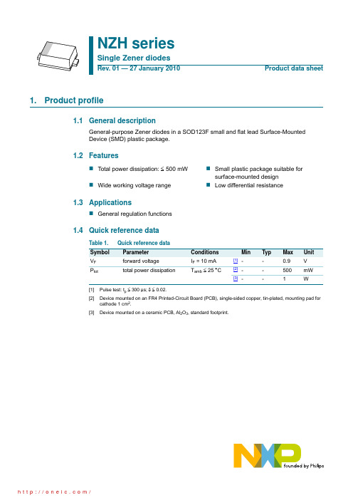
5. Limiting values
Table 5. Limiting values In accordance with the Absolute Maximum Rating System (IEC 60134).
Symbol Parameter
Conditions
Min
Max Unit
IF Ptot
NZHxxx
C2003系列 changjiang 连接器商品说明书

1.90±0.25
0.20 SEC:A-A
2.00±0.25
8.73±0.25 0.84
1.30 0.65
5.54±0.20
A B C
A B C
1.00
0.50
0.72 0.40
1.50±0.25 SEC:B-B
1.50±0.25
1.60±0.25
2.00mm pitch Crimp Terminal
2.00mm pitch wire to wire connector
0.20 2.40±0.25
2.68±0.25
3.00±0.25 0.80
1.30
1.50±0.25
A
A
B
B
1.50±0.20
7.50±0.25
1.60±0.25
SEC:A-A
B
2.00
5.70
4.00
7.70
6.00
9.70
8.00
11.70
10.00
13.70
14.00
17.70
18.00
21.70
Unit: mm
Reference Informations: *Material:Nylon 66,UL94V-0 *Suitable CJT C2003MB-T series Terminal *Mates with CJT C2003HFB-XP series Housing and C2003SB-XP series Seal *Color:White
5.20±0.20 9.20±0.25
2.10±0.20
2.70±0.25
三汇示波器说明书(Ver1.0)
DST4000 和 DST1000 系列数字存储示波器用户手册
i
目录
5.1 显示区 ........................................................................................ 20 5.2 信息区域..................................................................................... 23 5.3 波形显示..................................................................................... 23
三汇系列产品
DST4000 和 DST1000 系列 数字存储示波器
Version 1.0
杭州三汇科技有限公司 www.
目录
目录
目 录 ...........................................................................................................i 版权申明 .......................................................................................................................................................................v 第 1 章 安全事项......................................................................................... 1
萨姆导弹模拟器中文手册

微小型DM中文-C3更新版

l 2.8 2.8 3.2 3.2 3.5 3.5 2.8 2.8 3.5 3.5 4.5 4.5
L1 19.5 29.2 20.3 33.3 25.3 43.1 26.7 38.7 30.5 45.1 38.1 57.3
Oil-H Ø1.5 Ø1.5 Ø2 Ø2 M3 M3 Ø1.5 Ø1.5 Ø2 Ø2 M3 M3
T1 2.4 2.4 3 3 3.5 3.5 2.3 2.3 3 3 3.5 3.5
N 5 5 5 5
W1 9 9 12 12 15 15 18 18 24 24 42 42
H1 6.05 6.05 7.25 7.25 9.5 9.5 7.5 7.5 8.7 8.7 9.5 9.5
F 20 20 25 25 40 40 30 30 40 40 40 40
精度 : N : 普通級 H : 高 級 P : 精密級
滑塊類型 : N: 標準長度 L : 延伸長度
軌 長
2 支平行使用
股份有限公司
237 新北市三峽區三樹路168巷46號
電 話 :+886-2-26716600 傳 真 :+886-2-26711400
微小型dm中文c3更新版微小说中文幽默王微小病变型肾病微小型企业dm0265r中文资料dm100中文版下载dm分区工具中文版微小型企业贷款微小型朔料鱼缸微小型真空泵
Miniature Linear Guide
微 小 型 線.性.滑.軌
STAF 微小型 MB 系列 >>> 標準型 & 鏈帶型
W2
WH W1
E
h
Ød
MBX15WL
Mz
MB 系列規格尺寸表 >>> MBC 鏈帶型
成都新为诚 微型真空泵V30系列产品说明书

无刷微型真空泵V30系列产品说明书(Ver.2022.12.23)1产品版本及外观1.1V30(基础型)1.2V30(旋钮调速型)1.3V30(频率调速型)1.4V30(ding配型)2技术参数2.1关键参数注:1、该系列微型泵均使用直流电源,输入电压要求:DC24V±10%(24V型号泵)、DC12V±10%(12V型号泵);所需直流稳压电源为选配件,客户需自配,或也可从我司购买定做好的电源。
2、如无特别说明,技术参数均是在25℃、标准大气压101kPa的条件下的测定值;3、表中参数是在电机MAX转速时测得。
当转速变化时,压力/真空度基本不变;4、表中参数均在标配接口下测得,若选配其他类型接口,参数可能会发生小幅改变;5、表中峰值流量是指用玻璃转子流量计(去掉了针型阀)测得的流量值,平均流量是用皂膜流量计测得的流量值;不建议使用质量流量计进行测量,因原理等原因会导致较大误差(这不是微型泵的问题)。
6、该系列微型泵根据:(1)流量不同可分为:大流量-L,中流量-M,小流量-S;(2)性能、寿命、生产工艺、调试等不同,可分为简化版(简称J,下同)、标准版(B)、品质版(P);(3)功能不同,可细分为基础型(J)、旋钮调速型(X)、频率调速型(H)、ding配型(D);结合版本组合为:简化版-基础型(JJ)、标准版-旋钮调速型(BX)、标准版-频率调速型(BH)、品质版-旋钮调速型(PX)、品质版频率调速型(PH)、品质版-ding配型(PD)。
(4)是否可定做不同材质:①型号中带有后缀“B”的,可定做耐腐蚀材质(隔膜/单向阀材质:FKM(氟橡胶));②无后缀的,默认为:隔膜/单向阀材质:EPDM。
(4)【实例】(订购时,请一定注明流量、版本后缀!):①V30M-JJ-24V,意为V30微型真空泵中,中流量、简化版-基础型,DC24V供电;②V30S-PD-24V,意为V30微型真空泵中,小流量、品质版-ding配型,DC24V供电,品质MAX高,功能MAX齐全产品。
本特利3500中文说明介绍模板之欧阳育创编

TSI系统调试基本知识本内容将围绕大多数电厂中广泛使用的美国本特利(BENTLY)公司生产的振动检测系统3500为模版,全面讲述系统安装、组态、调试过程及调试中常见问题的处理。
第一节 TSI系统硬件基本知识3500系统能提供连续、在线监测功能,适用于机械保护应用,并为早期识别机械故障提供重要的信息。
该系统高度模块系统的工作流程是:从现场取得的传感器输入信号提供给3500监测器框架内的监测器和键相位通道,数据被采集后,与报警点比较并从监测器框架送到一个地方或多个地方处理。
3500框架中模件的共同特征是带电插拔和内部、外部接线端子。
任何主模件(安装在3500框架前端)能够在系统供电状态中拆除和更换而不影响不相关模块的工作,如果框架有两个电源,插拔其中一块电源不会影响3500框架的工作。
外部端子使用多芯电缆(每个模块一根线)把输入\输出模块与终端连接起来,这些终端设备使得在紧密空间内把多条线与框架连接起来变的非常容易,内部端子则用于把传感器与输入\输出模块直接连接起来。
外部端子块一般不能与内部端子输入/输出模块一起使用。
1、3500/05系统框架3500框架用于安装所有的监测器模块和框架电源。
它为3500各个框架之间的互相通讯提供背板通讯,并为每个模块提供所要求的电源。
3500框架有两种尺寸:1 全尺寸框架——19英寸EIA框架,有14个可用模块插槽2 迷你型框架——12英寸框架,有7个可用模块插槽电源和框架接口模块必须安装于最左边的两个插槽中。
其余14个框架位置(对与迷你型框架来说是其余7个位置)可以安装任何模块。
2、3500/15电源模块3500 电源是半高度模块,必须安装在框架左边特殊设计的槽口内。
3500 框架可装有一个或两个电源(交流或直流的任意组合)。
其中任何一个电源都可给整个框架供电。
如果安装两个电源,第二个电源可做为第一个电源的备份。
当安装两个电源时,上边的电源作为主电源,下边的电源作为备用电源,只要装有一个电源,拆除或安装第二个电源模块将不影响框架的运行。
- 1、下载文档前请自行甄别文档内容的完整性,平台不提供额外的编辑、内容补充、找答案等附加服务。
- 2、"仅部分预览"的文档,不可在线预览部分如存在完整性等问题,可反馈申请退款(可完整预览的文档不适用该条件!)。
- 3、如文档侵犯您的权益,请联系客服反馈,我们会尽快为您处理(人工客服工作时间:9:00-18:30)。
100 IF – Forward Current ( mA ) 50 Ptot=500mW Tamb=25°C
Tj = 25°C 1
IZ – Z-Current ( mA )
10
40
30
0.1 0.01 0.001 0 0.2 0.4 0.6 0.8 1.0
20 10 0 15 20 25 30 35
Figure 8. Z–Current vs. Z–Voltage
IZ – Z-Current ( mA )
80 Ptot=500mW Tamb=25°C 60
IZ=1mA 100
5mA 10 10mA
40 20 0 0 4 8 12 16 20
1 0
95 9606
Tj = 25°C 5 10 15 20 25
www.vishay.de • FaxBack +1-408-970-5600 1 (6)
元器件交易网
TZMC...
Vishay Telefunken
Type TZMC... 2V4 2V7 3V0 3V3 3V6 3V9 4V3 4V7 5V1 5V6 6V2 6V8 7V5 8V2 9V1 10 11 12 13 15 16 18 20 22 24 27 30 33 36 39 43 47 51 56 62 68 75 VZnom V 2.4 2.7 3.0 3.3 3.6 3.9 4.3 4.7 5.1 5.6 6.2 6.8 7.5 8.2 9.1 10 11 12 13 15 16 18 20 22 24 27 30 33 36 39 43 47 51 56 62 68 75 IZT mA 5 5 5 5 5 5 5 5 5 5 5 5 5 5 5 5 5 5 5 5 5 5 5 5 5 5 5 5 5 2.5 2.5 2.5 2.5 2.5 2.5 2.5 2.5 for VZT and V1) 2.28 to 2.56 2.5 to 2.9 2.8 to 3.2 3.1 to 3.5 3.4 to 3.8 3.7 to 4.1 4.0 to 4.6 4.4 to 5.0 4.8 to 5.4 5.2 to 6.0 5.8 to 6.6 6.4 to 7.2 7.0 to 7.9 7.7 to 8.7 8.5 to 9.6 9.4 to 10.6 10.4 to 11.6 11.4 to 12.7 12.4 to 14.1 13.8 to 15.6 15.3 to 17.1 16.8 to 19.1 18.8 to 21.2 20.8 to 23.3 22.8 to 25.6 25.1 to 28.9 28 to 32 31 to 35 34 to 38 37 to 41 40 to 46 44 to 50 48 to 54 52 to 60 58 to 66 64 to 72 70 to 79 rzjT rzjk at IZK W mA < 600 1 < 600 1 < 600 1 < 600 1 < 600 1 < 600 1 < 600 1 < 600 1 < 550 1 < 450 1 < 200 1 < 150 1 < 50 1 < 50 1 < 50 1 < 70 1 < 70 1 < 90 1 < 110 1 < 110 1 < 170 1 < 170 1 < 220 1 < 220 1 < 220 1 < 220 1 < 220 1 < 220 1 < 220 1 < 500 0.5 < 600 0.5 < 700 0.5 < 700 0.5 < 1000 0.5 < 1000 0.5 < 1000 0.5 < 1500 0.5 IR and IR at VR mA mA 2) V < 50 < 100 1 < 10 < 50 1 <4 < 40 1 <2 < 40 1 <2 < 40 1 <2 < 40 1 <1 < 20 1 < 0.5 < 10 1 < 0.1 <2 1 < 0.1 <2 1 < 0.1 <2 2 < 0.1 <2 3 < 0.1 <2 5 < 0.1 <2 6.2 < 0.1 <2 6.8 < 0.1 <2 7.5 < 0.1 <2 8.2 < 0.1 <2 9.1 < 0.1 <2 10 < 0.1 <2 11 < 0.1 <2 12 < 0.1 <2 13 < 0.1 <2 15 < 0.1 <2 16 < 0.1 <2 18 < 0.1 <2 20 < 0.1 <2 22 < 0.1 <2 24 < 0.1 <2 27 < 0.1 <5 30 < 0.1 <5 33 < 0.1 <5 36 < 0.1 < 10 39 < 0.1 < 10 43 < 0.1 < 10 47 < 0.1 < 10 51 < 0.1 < 10 56 TKVZ %/K –0.09 to –0.06 –0.09 to –0.06 –0.08 to –0.05 –0.08 to –0.05 –0.08 to –0.05 –0.08 to –0.05 –0.06 to –0.03 –0.05 to +0.02 –0.02 to +0.02 –0.05 to +0.05 0.03 to 0.06 0.03 to 0.07 0.03 to 0.07 0.03 to 0.08 0.03 to 0.09 0.03 to 0.1 0.03 to 0.11 0.03 to 0.11 0.03 to 0.11 0.03 to 0.11 0.03 to 0.11 0.03 to 0.11 0.03 to 0.11 0.04 to 0.12 0.04 to 0,12 0.04 to 0.12 0.04 to 0.12 0.04 to 0.12 0.04 to 0.12 0.04 to 0.12 0.04 to 0.12 0.04 to 0.12 0.04 to 0.12 0.04 to 0.12 0.04 to 0.12 0.04 to 0.12 0.04 to 0.12
95 9604
VZ – Z-Voltage ( V )
VZ – Z-Voltage ( V )
1000 – Voltage Change ( mV )
Figure 3. Typical Change of Working Voltage vs. Junction Temperature
TK VZ – Temperature Coefficient of VZ ( 10 –4 /K ) 15
Tj = 25°C 100
95 9605
VF – Forward Voltage ( V )
95 9607
VZ – Z-Voltage ( V )
Figure 6. Forward Current vs. Forward Voltage
100 r Z – Differential Z-Resistance ( W ) 1000
Figure 4. Temperature Coefficient of Vz vs. Z–Voltage
200 C D – Diode Capacitance ( pF )
150 VR = 2V 100 Tj = 25°C
50
0 0
95 9601
5
10
15
20
25
VZ – Z-Voltage ( V )
元器件交易网
TZMC...
Vishay Telefunken
Silicon Epitaxial Planar Z–Diodes
Features
D D D D D
Very sharp reverse characteristic Low reverse current level Available with tighter tolerances Very high stability Low noise
95 9602
1.3 VZtn – Relative Voltage Change VZtn=VZt/VZ(25°C) 1.2
TKVZ=10 10–4/K 8 6 10–4/K 10–4/K 10–4/K 10–4/K
1.1
4 2
1.0 0.9 0.8 –60
0 –2 10–4/K –4 10–4/K
Figure 5. Diode Capacitance vs. Z–Voltage
Document Number 85611 Rev. 3, 01-Apr-99
www.vishay.de • FaxBack +1-408-970-5600 3 (6)
元器件交易网
TZMC...
10
5 IZ=5mA 0
IZ=5mA 10
DVZ
1 0
95 9598
–5 0 10 20 30 40 50 VZ – Z-Voltage ( V )Leabharlann 51015
20
25
VZ – Z-Voltage ( V )
95 9600
Figure 2. Typical Change of Working Voltage under Operating Conditions at Tamb=25°C