TLGE53T中文资料
DTC114TM3T5G;DTC144WM3T5G;中文规格书,Datasheet资料
© Semiconductor Components Industries, LLC, 2011
1
August, 2011 − Rev. 5
/
Publication Order Number: DTC114EM3/D
DTC114EM3T5G Series
DEVICE MARKING AND RESISTOR VALUES
*Available upon request.
THERMAL CHARACTERISTICS
Characteristic
Total Device Dissipation, FR−4 Board (Note 1) @ TA = 25°C Derate above 25°C
Thermal Resistance, Junction−to−Ambient (Note 1)
100
DTC144WM3T5G*
8P
47
22
DTC144TM3T5G
8T
47
∞
†For information on tape and reel specifications, including part orientation and tape sizes, please refer to our Tape and Reel Packaging Specifications Brochure, BRD8011/D.
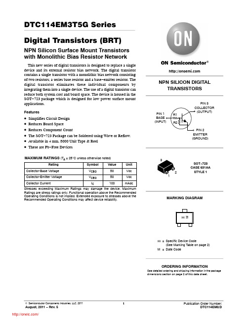
NPN SILICON DIGITAL TRANSISTORS
PIN 1
R1
BASE
(INPUT) R2
PIN 3 COLLECTOR
(OUTPUT)
PIN 2 EMITTER (GROUND)
3
L-53SRD-G中文资料

Notes: 1. All dimensions are in millimeters (inches). 2. Tolerance is ±0.25(0.01") unless otherwise noted. 3. Lead spacing is measured where the lead emerge package. 4. Specifications are subjected to change without notice.
元器件交易网
Kingbright
Features
®
T- 1 3/4 (5mm) SUPER BRIGHT LED LAMPS
L-53SG SUPER BRIGHT GREEN L-53SR SUPER BRIGHT RED
Package Dimensions
BRIGHTNESS. DIFFUSED AND WATER CLEAR LENS ARE AVAILABLE. lOUTSTANDING MATERIAL EFFICIENCY. lRELIABLE AND RUGGED. lIC COMPATIBLE/LOW CURRENT CAPABILITY.
Parameter
Power dissipation DC Forward Current Peak Forward Current [1] Reverse Voltage Operating/Storage Temperature Lead Soldering Temperature [2]
Notes: 1.1/10 Duty Cycle, 0.1ms Pulse Width. 2. 4mm below package base.
Super Bright Red L-53SRC / L-53SRD
VISHAY BYT53 说明书

BYT53.Document Number 86030Rev. 1.8, 14-Apr-05Vishay Semiconductors1949539Ultra Fast Avalanche Sinterglass DiodeFeatures•Glass passivated junction •Hermetically sealed package•Low reverse current•Soft recovery characteristics •Lead (Pb)-free component•Component in accordance to RoHS 2002/95/EC and WEEE 2002/96/ECApplicationsVery fast rectification and switches Switched mode power supplies High-frequency inverter circuitsMechanical DataCase: SOD-57 Sintered glass caseTerminals: Plated axial leads, solderable per MIL-STD-750, Method 2026Polarity: Color band denotes cathode end Mounting Position: Any Weight: approx. 369 mgParts TableAbsolute Maximum RatingsT amb = 25°C, unless otherwise specifiedPartType differentiationPackageBYT53A V R = 50 V; I FAV = 1.9 A SOD-57BYT53B V R = 100 V; I FAV = 1.9 A SOD-57BYT53C V R = 150 V; I FAV = 1.9 A SOD-57BYT53D V R = 200 V; I FAV = 1.9 A SOD-57BYT53F V R = 300 V; I FAV = 1.9 A SOD-57BYT53GV R = 400 V; I FAV = 1.9 ASOD-57ParameterT est conditionPart Symbol Value Unit Reverse voltage = Repetitive peak reverse voltagesee electrical characteristicsBYT53A V R = V RRM 50V BYT53B V R = V RRM 100V BYT53C V R = V RRM 150V BYT53D V R = V RRM 200V BYT53F V R = V RRM 300V BYT53GV R = V RRM400V Peak forward surge currentt p = 10 ms, half sinewaveI FSM50A 2Document Number 86030Rev. 1.8, 14-Apr-05BYT53.Vishay SemiconductorsMaximum Thermal ResistanceT amb = 25°C, unless otherwise specifiedElectrical CharacteristicsT amb = 25°C, unless otherwise specifiedTypical Characteristics (Tamb = 25 °C unless otherwise specified)Average forward current l = 10 mm, T L = 25°CI FAV 1.9A Junction and storage temperature range T j = T stg - 55 to + 175°C Non repetitive reverse avalanche energyI (BR)R = 1 AE R20mJParameterTest conditionPartSymbol Value Unit Junction ambientl = 10 mm, T L = constant R thJA 45K/W on PC board with spacing 25 mmR thJA100K/WParameterTest conditionPartSymbol MinTyp.Max Unit Forward voltage I F = 1 AV F 1.1V I F = 1 A, T j = 175°C V F 0.9V Reverse currentV R = V RRMI R 5µA V R = V RRM , T j = 150°C I R 200µA Reverse recovery timeI F = 0.5 A, I R = 1 A, i R = 0.25 At rr50nsParameterTest conditionPartSymbol ValueUnit Figure 1. Max. Thermal Resistance vs. Lead Length 00R -T h e r m .R e s i s t .J u n c t i o n /A m b i e n t (K /W )t h J A l -Lead Length (mm )94955251015253020Figure 2. Forward Current vs. Forward VoltageI-F o r w a r d C u r r e n t (A )0.010.111016333FBYT53.Document Number 86030Rev. 1.8, 14-Apr-05Vishay Semiconductors3Package Dimensions in mm (Inches)Figure 3. Max. Average Forward Current vs. Ambient TemperatureFigure 4. Reverse Current vs. Junction Temperature 0.00.20.40.60.81.01.21.41.61.82.020406080100120140160180T am b -J u nction Temperat u re (°C )16334I -A v e r a g e F o r w a r d C u r r e n t (A )F A V110100100025507510012515017516335I -R e v e r s e C u r r e n t (µA )R T j -J u nction Temperat u re (°C )Figure 5. Max. Reverse Power Dissipation vs. JunctionTemperatureFigure 6. Diode Capacitance vs. Reverse Voltage2040608010012014016018020022016336P -R e v e r s e P o w e r D i s s i p a t i o n (m W )R 255075100125150175T j -J u nction Temperat u re (°C)0102030405060R 16337C -D i o d e C a p a c i t a n c e (p F )D 4Document Number 86030 Rev. 1.8, 14-Apr-05BYT53.Vishay SemiconductorsOzone Depleting Substances Policy StatementIt is the policy of Vishay Semiconductor GmbH to1.Meet all present and future national and international statutory requirements.2.Regularly and continuously improve the performance of our products, processes, distribution and operatingsystems with respect to their impact on the health and safety of our employees and the public, as well as their impact on the environment.It is particular concern to control or eliminate releases of those substances into the atmosphere which are known as ozone depleting substances (ODSs).The Montreal Protocol (1987) and its London Amendments (1990) intend to severely restrict the use of ODSs and forbid their use within the next ten years. Various national and international initiatives are pressing for an earlier ban on these substances.Vishay Semiconductor GmbH has been able to use its policy of continuous improvements to eliminate the use of ODSs listed in the following documents.1.Annex A, B and list of transitional substances of the Montreal Protocol and the London Amendmentsrespectively2.Class I and II ozone depleting substances in the Clean Air Act Amendments of 1990 by the EnvironmentalProtection Agency (EPA) in the USA3.Council Decision 88/540/EEC and 91/690/EEC Annex A, B and C (transitional substances) respectively. Vishay Semiconductor GmbH can certify that our semiconductors are not manufactured with ozone depleting substances and do not contain such substances.We reserve the right to make changes to improve technical designand may do so without further notice.Parameters can vary in different applications. All operating parameters must be validated for each customer application by the customer. Should the buyer use Vishay Semiconductors products for any unintended or unauthorized application, the buyer shall indemnify Vishay Semiconductors against all claims, costs, damages, and expenses, arising out of, directly or indirectly, any claim of personal damage, injury or death associated with such unintended or unauthorized use.Vishay Semiconductor GmbH, P.O.B. 3535, D-74025 Heilbronn, GermanyLegal Disclaimer NoticeVishay Document Number: Revision: 08-Apr-051NoticeSpecifications of the products displayed herein are subject to change without notice. Vishay Intertechnology, Inc., or anyone on its behalf, assumes no responsibility or liability for any errors or inaccuracies.Information contained herein is intended to provide a product description only. No license, express or implied, by estoppel or otherwise, to any intellectual property rights is granted by this document. Except as provided in Vishay's terms and conditions of sale for such products, Vishay assumes no liability whatsoever, and disclaims any express or implied warranty, relating to sale and/or use of Vishay products including liability or warranties relating to fitness for a particular purpose, merchantability, or infringement of any patent, copyright, or other intellectual property right. The products shown herein are not designed for use in medical, life-saving, or life-sustaining applications. Customers using or selling these products for use in such applications do so at their own risk and agree to fully indemnify Vishay for any damages resulting from such improper use or sale.。
G1085T53T中文资料
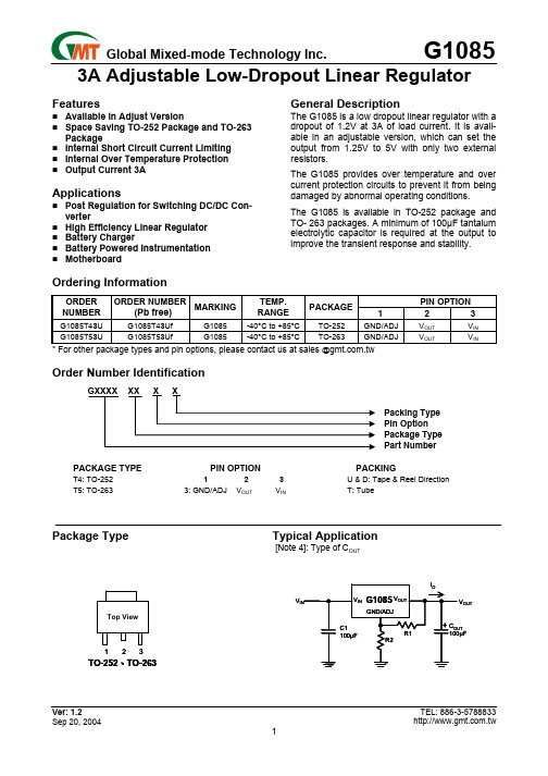
FeaturesAvailable in Adjust VersionSpace Saving TO-252 Package and TO-263 PackageInternal Short Circuit Current Limiting Internal Over Temperature ProtectionOutput Current 3AApplicationsPost Regulation for Switching DC/DC Con-verterHigh Efficiency Linear Regulator Battery ChargerBattery Powered InstrumentationMotherboardGeneral DescriptionThe G1085 is a low dropout linear regulator with a dropout of 1.2V at 3A of load current. It is avail-able in an adjustable version, which can set the output from 1.25V to 5V with only two external resistors.The G1085 provides over temperature and over current protection circuits to prevent it from being damaged by abnormal operating conditions. The G1085 is available in TO-252 package and TO- 263 packages. A minimum of 100µF tantalum electrolytic capacitor is required at the output to improve the transient response and stability.Ordering InformationPIN OPTIONORDER NUMBERORDER NUMBER(Pb free)MARKINGTEMP. RANGEPACKAGE1 2 3G1085T43U G1085T43Uf G1085 -40°C to +85°C TO-252 GND/ADJ V OUT V IN G1085T53U G1085T53UfG1085-40°C to +85°CTO-263GND/ADJV OUTV IN* For other package types and pin options, please contact us at sales @Order Number IdentificationType Pin Option TypePart NumberPACKAGE TYPE PIN OPTION PACKINGT4: TO-252 12 3 U & D: Tape & Reel Direction T5: TO-263 3: GND/ADJ V OUT V IN T: TubePackage Type Typical Application [Note 4]: Type of C OUTV V OUT123TO-252、TO-263Input Voltage…………………………….………………7V Power Dissipation Internally Limited (Note 2) Maximum Junction Temperature…...……………….150°C Storage Temperature Range…..…-65°C ≤ T J ≤+150°CReflow Temperature (soldering, 10sec)…………260°C Thermal Resistance Junction to AmbientTO-252(1)………………………………….………125°C/W TO-263(1)………………………………….………100°C/W Thermal Resistance Junction to CaseTO-252………….………………..………..….……10°C/W TO-263…..………………………...……..…………6°C/W ESD Rating (Human Body Model)……......................2kVNote (1): See Recommended Minimum Footprint(V IN -V ADJ ) Voltage………..…………...………..2.5V~5.5V Temperature Range……………..….….-40°C ≤ T A ≤85°C Electrical CharacteristicsOperating Conditions: V IN ≤ 7V, T A =T J = 25°C unless otherwise specified. [Note3]PARAMETER CONDITION MIN TYP MAX UNITReference Voltage V IN - V OUT = 2V, I OUT = 10mA1.2251.2501.275VLine Regulation(V OUT + 1.5V) < V IN < 7V, I OUT = 10mA --- 0.5 1 % Load Regulation (V IN - V OUT ) = 2V, 10mA < I OUT <3A --- 0.04 0.5 % Dropout Voltage ∆V OUT = 2%, I OUT = 3A --- 1.3 1.4 V Current Limit(V IN - V OUT ) = 2V---5.4---AAdjust Pin Current Change V IN - V OUT = 2V, 10mA < I OUT < 3A --- 0.15 --- µA Minimum Load Current 1.5V < (V IN - V OUT ) < 5.25V 10 --- --- mA Quiescent Current V IN - V OUT = 2V---80150µARipple Rejection f = 120Hz, C OUT = 10µF Tantalum,(V IN - V OUT ) = 3V, I OUT = 1A--- 48 --- dBTemperature StabilityV IN = 4V, I O =10mA --- 0.3 --- %RMS Output Noise (% of V OUT ) T A = 25°C, 10Hz < f < 10kHz, I LOAD = 10mA --- 0.007 --- %Thermal Shutdown Junction Temperature --- 150 --- °CThermal Shutdown Hysteresis--- 30 --- °CNote 1: Absolute Maximum Ratings are limits beyond which damage to the device may occur. Operating Con-ditions are conditions under which the device functions but the specifications might not be guaranteed. For guaranteed specifications and test conditions see the Electrical Characteristics.Note 2: The maximum power dissipation is a function of the maximum junction temperature, T Jmax ; total thermal re-sistance, θJA , and ambient temperature T A . The maximum allowable power dissipation at any ambient tem-perature is T jmax -T A / θJA . If this dissipation is exceeded, the die temperature will rise above 150°C and ICwill go into thermal shutdown.Note3: Low duty pulse techniques are used during test to maintain junction temperature as close to ambient as possible.Note4: The type of output capacitor should be tantalum or aluminum.Output VoltageThe G1085 provides an adjustable output voltage from 1.25V to 5V. with two external resistors. It can be for-mulated as:R2 V OUT = 1.25V x (1+R1) + IADJx R2I ADJ = 80µA (TYP)Dropout VoltageThe input/output Voltage differential at which the regulator output no longer maintains regulation against further reductions in input voltage. Measured when the output drops 2% below its nominal value. Dropout voltage is affected by junction temperature, load cur-rent and minimum input supply requirements. Line RegulationThe change in output voltage for a change in input voltage. The measurement is made under conditions of low dissipation or by using pulse techniques such that average chip temperature is not significantly af-fected.Load RegulationThe change in output voltage for a change in load current at constant chip temperature. The measure-ment is made under conditions of low dissipation or by using pulse techniques such that average chip tem-perature is not significantly affected.Maximum Power DissipationThe maximum total device dissipation for which the regulator will operate within specifications.Quiescent Bias CurrentCurrent which is used to operate the regulator chip and is not delivered to the load.(V IN -V OUT =3V, V OUT =1.25V, C IN =100µF, C OUT =100µF, T A =25°C, unless otherwise noted.)I L =100mALine Transient ResponseLoad Transient ResponseOutput NoiseShort Circuit-CurrentDropout Voltage vs. I OUTLoad RegulationOutput Voltage vs. TemperatureAdj Pin Current vs. TemperatureG1085T43(TO-252) Max. PowerDissipation vs. PCB Top CopperG1085T43(TO-252) Max. Power Dissipation vs. T AMB (still air)Recommend Minimum FootprintG1085T53(TO-263) Max. Power Dissipation vs. PCB Top Copper Area T = 25°C ; Still AirG1085T53(TO-263) Max. Power Dissipation vs. TAMB (still air)TO-252 (T4) PackageDIMENSION IN MILLIMETER DIMENSION IN INCHSYMBOLMIN. MAX. MIN. MAX.A 2.19 2.38 0.086 0.094 A1 0.89 1.27 0.035 0.050 b 0.64 0.89 0.025 0.035 C 0.46 0.58 0.018 0.023 D 5.97 6.22 0.235 0.245E 6.35 6.73 0.250 0.265 E1 5.21 5.46 0.2050.215 e 2.26 BSC 0.09 BSC e1 3.96 5.18 0.156 0.204 F 0.46 0.58 0.018 0.023 L1 0.89 2.03 0.035 0.080 L2 0.64 1.02 0.025 0.040 L3 2.40 2.80 0.095 0.110 H 9.40 10.40 0.370 0.410 θ 0° 4° 0° 4°TO-263 (T5) PackageMILLIMETER INCH SYMBOLMIN MAX MIN MAXA 4.30 4.70 0.169 0.185 A1 1.22 1.32 0.048 0.055 A2 2.45 2.69 0.104 0.106 b 0.69 0.94 0.027 0.037 b1 1.22 1.40 0.048 0.055 C 0.36 0.56 0.014 0.022 D 8.64 9.652 0.340 0.380 E 9.7010.54 0.382 0.415 e 2.29 2.79 0.090 0.110 e1 4.83 5.33 0.190 0.210 H 14.60 15.78 0.575 0.625 L 4.70 5.84 0.185 0.230 L1 1.20 1.778 0.047 0.070 L2 2.24 2.84 0.088 0.111 L3 1.40MAX 0.055MAXPackage OrientationPACKAGE Q’TY/REELTO-252 2,500 ea TO-263 1,000 eaGMT Inc. does not assume any responsibility for use of any circuitry described, no circuit patent licenses are implied and GMT Inc. reserves the right at any time without notice to change said circuitry and specifications.TO-252 Package OrientationTO-263 Package OrientationFeed DirectionFeed Direction。
TEA1753TN1,518;中文规格书,Datasheet资料

2.4 Flyback green features
Valley switching for minimum switching losses (NXP patented) Frequency reduction with adjustable minimum peak current at low-power operation to maintain high efficiency at low output power levels
3 ofductors
TEA1753T
HV start-up flyback controller with integrated PFC controller
5. Block diagram
3)&'5,9(5 3)& GULYHU
TEA1753T
HV start-up DCM/QR flyback controller with integrated DCM/QR PFC controller
Rev. 3 — 24 August 2012 Product data sheet
1. General description
The TEA1753T is the third generation of green Switched Mode Power Supply (SMPS) controller ICs. The TEA1753T combines a controller for Power Factor Correction (PFC) and a flyback controller. Its high level of integration allows the design of a cost-effective power supply with a very low number of external components. The special built-in green functions provide high efficiency at all power levels. This efficiency applies to quasi-resonant operation at high-power levels, quasi-resonant operation with valley skipping, as well as reduced frequency operation at lower power levels. At low-power levels, the PFC switches off to maintain high efficiency. During low-power conditions, the flyback controller switches to frequency reduction mode and limits the peak current to an adjustable minimum value. This mode ensures high efficiency at low-power and good standby power performance while minimizing audible noise from the transformer. The controller is switched to the power-down mode for no-load operation. In this mode, the controller is shut down for very low standby power applications. The TEA1753T is a Multi-Chip Module, (MCM), containing two chips. The proprietary high-voltage BCD800 process which makes direct start-up possible from the rectified universal mains voltage in an effective and green way. The second low voltage Silicon On Insulator (SOI) is used for accurate, high-speed protection functions and control. The TEA1753T enables the design of highly efficient and reliable supplies with power requirements of up to 250 W using the minimum number of external components. Remark: All values provided throughout this data sheet are typical values unless otherwise stated.
LCP液晶聚合物(特殊工程料)
LCP液晶聚合物(特殊工程料)典型应用范围LCP全称LIQUID CRYSTAL POLYMER,中文名称液晶聚合物!其具有高强度、高刚性、耐高温、收缩率低、尺寸稳定性高电绝缘性等十分优良,被用广范于电子零件和各种耐热小型电子零件、电气、光导纤维、汽车及宇航等领域。
注塑模工艺条件1. 料筒温度通常料筒温度、喷嘴温度、材料熔融温度如表所示。
如考虑到螺杆的使用寿命,可以缩小后部、中部、前部的温差。
为了防止喷嘴流涎,喷嘴温度可以比表中所示的温度低10℃,如果要提高流动性的话,所设温度可以比表中所示的温度高出20℃,但是必须注意下列情况。
降低料筒温度时:滞留时间过长,不会引起粒料在料筒中老化,也不会产生腐蚀性气体,所以滞留时间长一般不会产生什么大的问题。
但是,如果长时间中断成型的话,请降低料筒温度,再次成型时,以扔掉几模为好。
各品级成型时的料筒温度(℃)2. 模具温度LCP可成型的模具温度在30℃-150℃之间。
但是我们一般将模具温度设定在70℃-110℃左右。
为了缩短成型周期、防止飞边及变形,应选择低的模具温度;如果要求制品尺寸稳定(特别是用于高温条件下的制品),减少熔接缝的产生及解决充填不足等问题时,则应选择高的模具温度。
3. 可塑化螺杆的转速一般为100rpm。
如果是含玻纤或者含碳玻纤的材料(例:A130、A230等),为了防止玻纤被折断,我们必须选择比较低的转速。
此外,背压也尽可能低一点。
料筒温度设定为300℃时,材料在料筒内滞留时间对机械性能、颜色的影响如图4-18--图4-20所示。
无充填级A950在料筒内滞留15分钟,其机械性能略有降低。
而A130在料筒内滞留60分钟,其机械性能基本保持不变。
无任是A950还是A130在颜色方面都有一点变化(△E)。
通过热天平所得到的失重情况如图4-21所示。
渐渐地开始分解的温度大约为460℃,比通常的成型温度要高出许多。
4. 注射压力和注射速度最合适的注射压力必须取决于材料、制品形状、模具设计(特别是直浇口、流道、浇口)及其他的成型条件。
汽车吊结构图与性能表
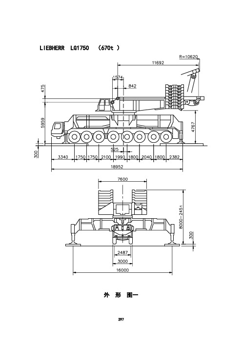
LIEBHERR LG1750 (670t )外形图一LG1750 (670t )外形图二LG1750 (670t )外形图三LG1750 (670t )R(m)H( )m 020*******48121624283236444852566468727684m4812162024283236404448525660646872768084889296100m主臂起升高度图一LG1750 主臂起重性能表一(支腿16×16m, 360°,配重850t)支腿尺寸16000×16000, 行驶速度80km/h,吊钩重量:750t-—-16000KG, 400t——-15000KG,312t--—8400KG,215t—--7500KG,107t——-5500KG,47t——-3000KG,16t-——1100KG。
LG1750 (670t )R(m)H( )m 020*******48121624283236444852566468727684m4812162024283236404448525660646872768084889296100m主臂起升高度图二LG1750 主臂起重性能表二(支腿12×12m, 360°,配重830t)LG1750 (670t )048121620242832364044485256606468727680m4812162024283236404448525660646872768084889296100104108112116120124128132136140144148mR(m)H ( )m主臂起升高度图三LG1750 主臂起重性能表三LG1750 (670t )R(m)H ( )m 081624324048566472808896104112m04812162024283236404448525660646872768084889296100104108112116120124128132136140144148152156160164168m副臂起升高度图LG1750 副臂起重性能表一LG1750 副臂起重性能表二(全支腿,16×16m,360°,配重850t)LG1750 副臂起重性能表三(全支腿,16×16m,360°,配重850t)DEMAG AC700 (700t)外形图DEMAG AC700 (700t )H ( )mR(m)5550454035302520151050051015202530354045505560657075808590mHA 工况起升高度图AC700 HA工况主臂起重性能表一b—-—-表示在吊机后部需加重型装置.总机全长20655,高4000,宽8754。
74LVC1G53资料

74LVC1G53
2-channel analog multiplexer/demultiplexer
Rev. 03 — 29 August 2007
Product data sheet
1. General description
The 74LVC1G53 is a low-power, low-voltage, high-speed, Si-gate CMOS device.
Rev. 03 — 29 August 2007
© NXP B.V. 2007. All rights reserved.
2 of 22
元器件交易网
NXP Semiconductors
6. Pinning information
6.1 Pinning
74LVC1G53
Z1 E2 GND 3 GND 4
The 74LVC1G53 provides one analog multiplexer/demultiplexer with a digital select input (S), two independent inputs/outputs (Y0 and Y1), a common input/output (Z) and an active LOW enable input (E). When pin E is HIGH, the switch is turned off.
For XSON8 and XQFN8 packages: above 45 °C the value of Ptot derates linearly with 2.4 mW/K.
74LVC1G53_3
Product data sheet
- 1、下载文档前请自行甄别文档内容的完整性,平台不提供额外的编辑、内容补充、找答案等附加服务。
- 2、"仅部分预览"的文档,不可在线预览部分如存在完整性等问题,可反馈申请退款(可完整预览的文档不适用该条件!)。
- 3、如文档侵犯您的权益,请联系客服反馈,我们会尽快为您处理(人工客服工作时间:9:00-18:30)。
TOSHIBA InGaA ℓP LEDTLRE53T,TLRME53T,TLSE53T,TLOE53T,TLYE53T,TLPYE53T,TLGE53T,TLFGE53T,TLPGE53TPanel Circuit Indicators· φ3 mm package · InGaA ℓP technology · All plastic mold · Transparent lens· Line-up: 6 colors (red, orange, yellow, pure yellow, green and puregreen) · High intensity light emission ·Excellent low current light output· Applications: message boards, security devices and dashboarddisplaysLine-upUnit: mmJEDEC ― JEITA―TOSHIBA 4-4E1A Weight: 0.14 gProduct NameColorMaterialTLRE53T RedTLRME53T Red TLSE53T Red TLOE53T OrangeTLYE53T YellowTLPYE53T Pure Yellow TLGE53T Green TLFGE53T Green TLPGE53T Pure GreenP InGaA lMaximum Ratings (Ta = 25°C)Product Name Forward CurrentI F (mA)Reverse VoltageV R (V)Power DissipationP D (mW)OperatingTemperatureT opr (°C)StorageTemperatureT stg (°C)TLRE53T 50 4 120TLRME53T 50 4 120TLSE53T 50 4 120TLOE53T 50 4 120TLYE53T 50 4 120TLPYE53T 50 4 120TLGE53T 50 4 120TLFGE53T 50 4 120TLPGE53T 50 4 120-40~100 -40~120 Electrical and Optical Characteristics (Ta = 25°C)Typ. Emission Wavelength Luminous IntensityI VForward VoltageV FReverse CurrentI RProduct Namel d l P Dl I F Min Typ.I F Typ.Max I F Max V R TLRE53T 630 (644) 20 20 153 400 20 1.9 2.4 20 50 4 TLRME53T 626 (636) 23 20 272 600 20 1.9 2.4 20 50 4 TLSE53T 613 (623) 20 20 272 800 20 1.9 2.4 20 50 4 TLOE53T 605 (612) 20 20 272 100020 2.0 2.4 20 50 4 TLYE53T 587 (590) 17 20 272 800 20 2.0 2.4 20 50 4 TLPYE53T 580 (583) 14 20 153 450 20 2.0 2.4 20 50 4 TLGE53T 571 (574) 17 20 153 400 20 2.0 2.4 20 50 4 TLFGE53T 565 (568) 15 20 85 200 20 2.0 2.4 20 50 4 TLPGE53T 558 (562) 14 20 47.6130 20 2.1 2.4 20 50 4 Unit nmmAmcdmAVmAm A V PrecautionsPlease be careful of the following:· Soldering temperature: 260°C max, soldering time: 3 s max(soldering portion of lead: up to 2 mm from the body of the device)· If the lead is formed, the lead should be formed up to 5 mm from the body of the device without forming stress to the resin. Soldering should be performed after lead forming.· This visible LED lamp also emits some IR light.If a photodetector is located near the LED lamp, please ensure that it will not be affected by this IR light.1.61.7 1.8 1.92.0 2.1 2.2 2.3Forward voltage V F (V) I F – V FF o r w a r d c u r r e n t I F (m A )Forward current I F (mA)I V – I FL u m i n o u s i n t e n s i t y I V (m c d )I V – TcR e l a t i v e l u m i n o u s i n t e n s i t y I VRelative luminous intensity – WavelengthAmbient temperature Ta (°C)90 1.00.80.6 0.4 0.2 0 8010110012020406080 1001.61.7 1.8 1.92.0 2.1 2.2 2.3R e l a t i v e l u m i n o u s i n t e n s i t yForward voltage V F (V) I F – V FF o r w a r d c u r r e n t I F (m A )Forward current I F (mA)I V – I FL u m i n o u s i n t e n s i t y I V (m c d )Case temperature Tc (°C)I V – TcR e l a t i v e l u m i n o u s i n t e n s i t y I VWavelength l (nm)Relative luminous intensity – WavelengthAmbient temperature Ta (°C)I F – TaRadiation pattern90 1.00.80.6 0.4 0.2 0 80°012020406080 100 20 -20 800.1310.30.50 4060 510700680 660 640 6206005801011001.61.7 1.8 1.92.0 2.1 2.2 2.3R e l a t i v e l u m i n o u s i n t e n s i t yForward voltage V F (V) I F – V FF o r w a r d c u r r e n t I F (m A )Forward current I F (mA)I V – I FL u m i n o u s i n t e n s i t y I V (m c d )Case temperature Tc (°C)I V – TcR e l a t i v e l u m i n o u s i n t e n s i t y I VWavelength l (nm)Relative luminous intensity – WavelengthAmbient temperature Ta (°C)I F – TaA l l o w a b l e f o r w a r d c u r r e n t I F (m A )Radiation patternTa = 25°C30°0°60° 90° 90°30°60° 1.00.80.6 0.4 0.2 0 80° 70° 50° 40°20°10°70°80°50°40°20°10°10110060040802012020406080 100 680660 640 620 60058056020 -20 800.1310.30.50 40601.61.7 1.8 1.92.0 2.1 2.2 2.3R e l a t i v e l u m i n o u s i n t e n s i t yForward voltage V F (V) I F – V FF o r w a r d c u r r e n t I F (m A )Forward current I F (mA)I V – I FL u m i n o u s i n t e n s i t y I V (m c d )Case temperature Tc (°C)I V – TcR e l a t i v e l u m i n o u s i n t e n s i t y I VWavelength l (nm)Relative luminous intensity – WavelengthAmbient temperature Ta (°C)I F – TaRadiation pattern90 1.00.80.6 0.4 0.2 0 80°012020406080 100 660640 620 600 58056054020 -20 800.1310.30.50 4060 1011001.61.7 1.8 1.92.0 2.1 2.2 2.3R e l a t i v e l u m i n o u s i n t e n s i t yForward voltage V F (V) I F – V FF o r w a r d c u r r e n t I F (m A )Forward current I F (mA)I V – I FL u m i n o u s i n t e n s i t y I V (m c d )Case temperature Tc (°C)I V – TcR e l a t i v e l u m i n o u s i n t e n s i t y I VWavelength l (nm)Relative luminous intensity – WavelengthAmbient temperature Ta (°C)I F – TaRadiation pattern90 1.00.80.6 0.4 0.2 0 80°012020406080 100 660640 620 600 58056054020 -20 800.1310.30.50 4060 1011002.0 1.62.31.7 2.1 1.8 1.9 2.2R e l a t i v e l u m i n o u s i n t e n s i t yForward voltage V F (V) I F – V FF o r w a r d c u r r e n t I F (m A )Forward current I F (mA)I V – I FL u m i n o u s i n t e n s i t y I V (m c d )Case temperature Tc (°C)I V– TcR e l a t i v e l u m i n o u s i n t e n s i t y I VWavelength l (nm)Relative luminous intensity – WavelengthAmbient temperature Ta (°C)I F – TaRadiation pattern90 1.00.80.6 0.4 0.2 0 80°012020406080 100 580540660560600 620 640 20 -20 8050.131010.30.50 40 60 1011001.61.7 1.8 1.92.0 2.1 2.2 2.3R e l a t i v e l u m i n o u s i n t e n s i t yForward voltage V F (V) I F – V FF o r w a r d c u r r e n t I F (m A )Forward current I F (mA)I V – I FL u m i n o u s i n t e n s i t y I V (m c d )Case temperature Tc (°C)I V – TcR e l a t i v e l u m i n o u s i n t e n s i t y I VWavelength l (nm)Relative luminous intensity – WavelengthAmbient temperature Ta (°C)I F – TaRadiation pattern90 1.00.80.6 0.4 0.2 0 80°012020406080 100 640620 600 580 56054052010110020 -20 800.1310.30.50 4060 5102.0 1.62.31.72.1 1.8 1.9 2.2R e l a t i v e l u m i n o u s i n t e n s i t yForward voltage V F (V) I F – V FF o r w a r d c u r r e n t I F (m A )Forward current I F (mA)I V – I FL u m i n o u s i n t e n s i t y I V (m c d )Case temperature Tc (°C)I V – TcR e l a t i v e l u m i n o u s i n t e n s i t y I VWavelength l (nm)Relative luminous intensity – WavelengthAmbient temperature Ta (°C)I F– TaRadiation pattern90 1.00.80.6 0.4 0.2 0 80°012020406080 100 560520640540580 600 620 20 -208050.131010.30.50 40 60 101100TLPGE53TR e l a t i v e l u m i n o u s i n t e n s i t yForward voltage V F (V) I F – V FF o r w a r d c u r r e n t I F (m A )Forward current I F (mA)I V – I FL u m i n o u s i n t e n s i t y I V (m c d )Case temperature Tc (°C)I V – TcR e l a t i v e l u m i n o u s i n t e n s i t y I VWavelength l (nm)Relative luminous intensity – WavelengthAmbient temperature Ta (°C)I F – TaA l l o w a b l e f o r w a r d c u r r e n t I F (m A )Radiation patternTa = 25°C1.61.7 1.8 1.92.0 2.1 2.2 2.330°0°60° 90° 90°30°60° 1.00.80.6 0.4 0.2 0 80° 70° 50° 40°20°10°70°80°50°40°20°10°10110060040802012020406080 100 20 -20 800.1310.30.50 4060 510640620 600 580 560540520· TOSHIBA is continually working to improve the quality and reliability of its products. Nevertheless, semiconductor devices in general can malfunction or fail due to their inherent electrical sensitivity and vulnerability to physical stress. It is the responsibility of the buyer, when utilizing TOSHIBA products, to comply with the standards of safety in making a safe design for the entire system, and to avoid situations in which a malfunction or failure of such TOSHIBA products could cause loss of human life, bodily injury or damage to property.In developing your designs, please ensure that TOSHIBA products are used within specified operating ranges as set forth in the most recent TOSHIBA products specifications. Also, please keep in mind the precautions and conditions set forth in the “Handling Guide for Semiconductor Devices,” or “TOSHIBA Semiconductor Reliability Handbook” etc.. · The TOSHIBA products listed in this document are intended for usage in general electronics applications (computer, personal equipment, office equipment, measuring equipment, industrial robotics, domestic appliances, etc.). These TOSHIBA products are neither intended nor warranted for usage in equipment that requires extraordinarily high quality and/or reliability or a malfunction or failure of which may cause loss of human life or bodily injury (“Unintended Usage”). Unintended Usage include atomic energy control instruments, airplane or spaceship instruments, transportation instruments, traffic signal instruments, combustion control instruments, medical instruments, all types of safety devices, etc.. Unintended Usage of TOSHIBA products listed in this document shall be made at the customer’s own risk. · Gallium arsenide (GaAs) is a substance used in the products described in this document. GaAs dust and fumes are toxic. Do not break, cut or pulverize the product, or use chemicals to dissolve them. When disposing of the products, follow the appropriate regulations. Do not dispose of the products with other industrial waste or with domestic garbage. · The information contained herein is presented only as a guide for the applications of our products. No responsibility is assumed by TOSHIBA CORPORATION for any infringements of intellectual property or other rights of the third parties which may result from its use. No license is granted by implication or otherwise under any intellectual property or other rights of TOSHIBA CORPORATION or others. · The information contained herein is subject to change without notice.000707EACRESTRICTIONS ON PRODUCT USE。