TLP421F中文资料
LN1F04 08 13 15力生美电源管理芯片

LN1F04/LN1F08/LN1F13/LN1F15/描述:LN1F08 为高性能、电流模式 PWM 控制器功率开关集成电路。
芯片内置高压功率开关,耐压高达750V以上,在85-300Vac的全球电网电压范围内提供高达 6W 的连续输出功率。
芯片采用前端稳压的反馈拓扑结构设计,无需光耦等二次侧反馈器件即可实现输出电压的稳定工作,且不受输入电压影响。
芯片可工作于典型的反激电路拓扑中,构成简洁的 AC/DC 电源转换器系统,用于电器控制板、电机驱动器等产品中。
IC 内部的倍流式高压启动电流源只需借助 VIN 电阻提供的微弱电流触发即可完成系统启动,很大程度地降低了 VINLN1F13 是新一代的高性能、高集成度电流模式PSR 功率开关集成电路,可以方便地在高达5.5W的应用中构建满足CoC V5 及DoE LEVEL VI 等能效标准的低待机功耗、高转换效率、高性能的PSR初级侧CC/CV 开关电源解决方案。
芯片内置高精度恒流恒压控制并具有优化的谷底开关技术,可在全范围提供优于±3% 精度的输出电流误差和±2% 精度的输出电压误差。
最高达70kHz 的开关频率允许使用相对较小的变压器尺寸完成设计,同时极小的死区时间控制使系统可工作在接近临界导通模式从而提高变压器的利用率,远优于传统的PSR 控制器架构。
LN1F15 是新一代的高性能、高集成度电流模式PSR 功率开关集成电路,可以方便地在高达 12W的应用中构建满足 CoC V5 及 DoE LEVEL VI 等能效标准的低待机功耗、高转换效率、高性能的 PSR初级侧 CC/CV 开关电源解决方案。
芯片内置高精度恒流恒压控制并具有优化的谷底开关技术,可在全范围提供优于±3% 精度的输出电流误差和±2% 精度的输出电压误差。
最高达 70kHz 的开关频率允许使用相对较小的变压器尺寸完成设计,同时极小的死区时间控制使系统可工作在接近临界导通模式从而提高变压器的利用率,远优于传统的 PSR 控制器架构主要特點❖前端穩壓限流結構控制方式無需光耦❖高低壓引腳兩側分佈的高隔離結構❖芯片內置 750V 高壓功率開關❖芯片內置 750V 倍流高壓電流源❖0.25W 以下的待機模式控制電路❖具有 EN 使能端子可外部關斷輸出❖輸出短路與芯片過溫度保護功能❖自適應週期回轉設計減小 EMI 干擾❖高轉換效率滿足 EUP 2013 能效要求❖全電網電壓下額定輸出功率 6W 以上❖電路簡潔外圍元件少系統成本低 應用領域✧家電控制板電源✧小型電機驅動電源✧個人護理產品電源✧其它線性電源替代電阻的功率消耗;而在輸出功率較小時IC將自動降低工作頻率,從而實現了很低的待機功耗和輕載效率;專利的驅動電路使開關管始終工作於臨界飽和狀態,提高了電源的轉換效率,使系統可以輕鬆滿足2013年乃至未來的多種能效標準,包括容易地實現0.25W待機要求。
LM324F资料

TLP554中文资料

tELH tEHL CMH
CML
RL=350W VE=0.5®3.0V
2
CL=15pF
IF=7.5 mA VE=3.0®0.5V
VCM=400V
IF=0mA VO(Min)=2.0V
3
RL=350W
IF=7.5mA (Note 7) VO(Max)=0.8V
(Note 7) CMHּThe maximum tolerable rate of rise of the common mode voltage to ensure the output will remain in the high state(i.e.,VOUT>2.0V) CMLּThe maximum tolerable rate of fall of the common mode voltage to ensure the output will remain in the low output state(i.e.,VOUT<0.8V) Measured in volts per microsecond(V/ms).
¾
¾
5
mA
Supply Current
High Level Low Level
ICCH ICCL
VCC=5.5V VE=0.5V
IF=0mA IF=10mA
¾
7
15
mA
¾
12
19
Enable Current
High Level Low Level
BF421-AP;中文规格书,Datasheet资料

BF421SMALL SIGNAL PNP TRANSISTORPRELIMINARY DATAsSILICON EPITAXIAL PLANAR PNP HIGH VOLTAGE TRANSISTORsTO-92 PACKAGE SUITABLE FOR THROUGH-HOLE PCB ASSEMBLY sTHE NPN COMPLEMENTARY TYPE IS BF420APPLICATIONS s VIDEO AMPLIFIER CIRCUITS (RGB CATHODE CURRENT CONTROL)s TELEPHONE WIRELINE INTERFACE (HOOK SWITCHES, DIALER CIRCUITS)®February 2003ABSOLUTE MAXIMUM RATINGS1/5s Pr od u c t () -l sOb so e t ePr od u c t () THERMAL DATAELECTRICAL CHARACTERISTICS (T case = 25 oC unless otherwise specified)BF421BF421BF421l s l c )Ob so e t ePr od u c t () -O bs o e t eP r od u t (sInformation furnished is believed to be accurate and reliable. However, STMicroelectronics assumes no responsibility for the consequences of use of such information nor for any infringement of patents or other rights of third parties which may result from its use. No license is granted by implication or otherwise under any patent or patent rights of STMicroelectronics. Specification mentioned in this publication are subject to change without notice. This publication supersedes and replaces all information previously supplied. STMicroelectronics products are not authorized for use as critical components in life support devices or systems without express written approval of STMicroelectronics.The ST logo is a trademark of STMicroelectronics © 2003 STMicroelectronics – Printed in Italy – All Rights ReservedSTMicroelectronics GROUP OF COMPANIESAustralia - Brazil - Canada - China - Finland - France - Germany - Hong Kong - India - Israel - Italy - Japan - Malaysia - Malta - Morocco - Singapore - Spain - Sweden - Switzerland - United Kingdom - United States.BF421分销商库存信息: STMBF421-AP。
TEP-I-F说明书1要点
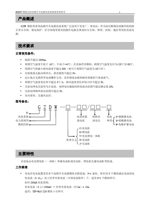
产品概述GZDW 微机型系列高频开关电源直流系统广泛适用于发电厂、变电站,作为高压断路直流操作机构的正常分合闸、继电保护、信号母线等使用的操作电源及事故时分合闸、照明、控制、通信等用的直流电源。
技术要求正常使用条件:•海拔不超过2000m。
•周围空气温度不低于-10℃,不高于+45℃,在设备停用期间,周围空气温度允许为-25℃至+50℃。
•周围空气的最大相对湿度不超过98%(相当于周围空气温度为25℃时)。
•安装地基无振动和冲击,垂直倾度不超过5%。
•运行地点无剧烈导电或爆炸尘埃,没有腐蚀金属和破坏绝缘的气体或蒸气。
•周围空气温度变化率不超过5℃/h,相对温度变化率每小时不超过5%。
•交流电网电压波形为正弦波,电网电压幅值的持续波动范围不超过额定值20%。
•交流电网频率波动范围不超过5%。
•室内使用,且通风良好。
型号命名:G-镉镍蓄电池或电流流电压种类 Q-铅酸蓄电池 M-免维护蓄电池 C-充电柜K-馈电柜Y-充电馈电一体柜柜体含义 D-电池柜J-交流柜主要特性本设备由充电馈电柜(一体柜)和蓄电池柜或充电柜、馈电柜及蓄电池柜等组成。
工作原理•充电浮充电装置采用多个高频开关电源模块并联组成,N+1备份,即在用N个模块满足电池的充电电流(0.1C10)加上经常负荷电流(合闸电流除外)下,选用N+1个模块即可。
如对200AH直流系统:充电电流(0.1×200AH)+ 经常负荷电流(约5A)= 25A•系统可以选用任何接线型式,其典型接线方式见《GZDW微机自控高频开关电源直流系统典型设计》(泰坦公司)。
•系统输出特性:系统输出特性见图1。
1.均衡充电状态为从图1中A点开始充电,A-B之间的区域为恒流充电区域;2.当蓄电池电压上升至均衡充电电压值B点后设备进入恒压充电工作方式,B-C段为恒定电压区域,均衡充电在给定的时间内结束。
均衡充电结束后,自动转换到浮充电压状态,蓄电池持续在完全充满状态,在D-A段工作。
BF421中文资料

Characteristic Symbol Min Max Unit
ON CHARACTERISTICS
DC Current Gain (IC = –25 mA, VCE = –20 Vdc) Collector – Emitter Saturation Voltage (IC = –20 mAdc, IB = –2.0 mAdc) Base – Emitter Saturation Voltage (IC = –20 mA, IB = –2.0 mA) hFE BF421 BF423 VCE(sat) VBE(sat) 50 50 — — — — –0.5 –2.0 Vdc Vdc —
2
Motorola Small–Signal Transistors, FETs and Diodes Device Data
元器件交易网
150 100 hFE, DC CURRENT GAIN +25°C 70 50 –55°C TJ = +125°C
BF421 BF423
0 –1.0
–2.0
–5.0 –10 –20 IC, COLLECTOR CURRENT (mA)
–50
–100
Figure 2. Capacitances
Figure 3. Current–Gain — Bandwidth Product
–1.0 IC, COLLECTOR CURRENT (mA)
ELECTRICAL CHARACTERISTICS (TA = 25°C unless otherwise noted)
TLP222G(TP1,F),TLP222G(TP1,F),TLP222G(TP1,F), 规格书,Datasheet 资料
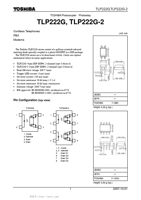
TOSHIBA Photocoupler Photorelay
TLP222G, TLP222G-2
Cordless Telephones PBX Modems
Unit: mm
The Toshiba TLP222G series consist of a gallium arsenide infrared emitting diode optically coupled to a photo-MOSFET in a DIP package.
Allowable On-sate current ION (mA)
TLP222G,TLP222G-2
ION – Ta
240
200
160
120
80
40
0
−20
0
20
40
60
80 100 120
Ambient temperature Ta (°C)
Forward current IF (mA)
100 Ta = 25°C
0
20
40
60
80
100
Ambient temperature Ta (°C)
4
芯天下--/
2007-10-01
On-state resistance RON (Ω)
Switching time tON, tOFF (μs)
50
Isolation Characteristics (Ta = 25°C)
Characteristics Capacitance input to output Isolation resistance
Isolation voltage
TLP421(东芝)

TOSHIBA Photocoupler GaAs Ired & Photo−TransistorTLP421Office EquipmentHousehold AppliancesSolid State RelaysSwitching Power SuppliesVarious ControllersSignal Transmission Between Different Voltage CircuitsThe TOSHIBA TLP421 consists of a silicone photo−transistor opticallycoupled to a gallium arsenide infrared emitting diode in a four leadplastic DIP (DIP4) with having high isolation voltage(AC: 5kV RMS (min)).· Collector-emitter voltage: 80V (min.)· Current transfer ratio: 50% (min.)Rank GB: 100% (min.)· Isolation voltage: 5000V rms (min.)· UL recognized: UL1577· BSI approved: BS EN60065: 1994Approved no.8411BS EN60950: 1992Approved no.8412· SEMKO approved: EN60065, EN60950, EN60335 Approvedno.9910249/01Pin Configurations(top view)1241 : Anode2 : Cathode3 : Emitter4 : CollectorUnit in mmTOSHIBA 11−5B2 Weight: 0.26 g· Option(D4)typeTÜV approved: DIN VDE0884Approved no.R9950202 Maximum operating insulation voltage: 890V PKMaximu permissible overvoltage: 8000V PK (Note): When a VDE0884 approved type is needed,please designate the “Option(D4)”Making the VDE applocation: DIN VDE0884 · Construction mechanical rating7.62mm Pich Typical Type 10.16mm Pich TLPxxxF Type Creepage distance7.0mm(min)8.0mm(min)Clearance 7.0mm(min) 8.0mm(min) Insulation thickness0.4mm(min)0.4mm(min)Current Transfer RatioCurrent Transfer Ratio (%)(I C / I F )I F = 5mA, V CE = 5V, Ta = 25°CTypeClassi -fication (*1) Min MaxMarking Of Classification(None) 50 600 Blank, Y, Y+, G, G+, B, B+, GB Rank Y50 150 Y, Y+ Rank GR 100 300 G, G+ Rank BL 200 600 B, B+TLP421Rank GB100600G, G+, B, B+, GB(*1): Ex. rank GB: TLP421 (GB)(Note): Application type name for certification test, please use standard product type name, i. e. TLP421 (GB): TLP421Maximum Ratings (Ta = 25°C)Characteristic Stmbol Rating UnitForward currentI F 60 mA Forward current derating(Ta ≥ 39°C) ∆I F / °C-0.7mA / °CPulse forward current (Note 2)I FP 1 A Power dissipation P D 100 mW Power dissipation derating ∆P D / °C-1.0 mW / °CReverse voltage V R 5 V L E DJunction temperature T j 125 °C Collector -emitter voltage V CEO 80 V Emitter -collector voltage V ECO 7 V Collector currentI C 50 mA Power dissipation(single circuit) P C 150 mW Power dissipation derating(Ta ≥ 25°C)(single circuit) ∆P C / °C-1.5 mW / °CD e t e c t o rJunction temperature T j 125 °C Operating temperature range T opr -55~100 °C Storage temperature range T stg-55~125 °CLead soldering temperature (10s) T sol 260 °C Total package power dissipation P T 250 mW Total package power dissipation derating (Ta ≥ 25°C) ∆P T / °C-2.5 mW / °CIsolation voltage(Note 3) BV S 5000 V rms(Note 2): 100µs pulse, 100Hz frequency(Note 3): AC, 1 min., R.H.≤ 60%. Apply voltage to LED pin and detector pin together.Recommended Operating ConditionsCharacteristic Symbol Min Typ. Max UnitSupply voltage V CC ―5 24 VForward current I F ― 16 25 mA Collector current I C ― 1 10 mA Operating temperatureT opr-25―85 °CIndividual Electrical Characteristics (Ta = 25°C)Characteristic Symbol Test Condition MinTyp. Max Unit Forward voltage V F I F = 10 mA 1.0 1.21.3VReverse currentI RV R = 5 V ―― 10 µAL E DCapacitance C T V = 0, f = 1 MHz ― 30 ― pF Collector -emitterbreakdown voltage V (BR) CEO I C = 0.5 mA 80 ― ― V Emitter -collector breakdown voltageV (BR) ECOI E = 0.1 mA7― ― V V CE = 24 V (ambient lightbelow 1000 ℓx) ―0.01 (0.1) 0.1 (10) µA Collector dark currentI D (I CEO )V CE = 24 V (ambient light Ta = 85°C below 1000 ℓx) ―0.6 (1)50 (50)µAD e t e c t o rCapacitance(collector to emitter)C CEV = 0, f = 1 MHz― 10 ― pFCoupled Electrical Characteristics (Ta = 25°C)Characteristic Symbol Test Condition MInTyp. Max Unit 50 ― 600 Current transfer ratioI C / I FI F = 5 mA, V CE = 5 VRank GB100― 600%― 60 ― Saturated CTRI C / I F (sat)IF = 1 mA, V CE = 0.4 VRank GB 30 ― ― %I C = 2.4 mA, I F = 8 mA―― 0.4― 0.2 ― Collector -emitter saturationvoltageV CE (sat)I C = 0.2 mA, I F = 1 mARank GB ― ― 0.4VIsolation Characteristics (Ta = 25°C)Characteristic Symbol Test Condition MinTyp. Max UnitCapacitance(input to output) C S V S = 0, f = 1 MHz ― 0.8 ― pF Isolation resistanceR SV S = 500 V 1×10¹² 1014 ― Ω AC, 1 minute5000――AC, 1 second, in oil ― 10000 ―V rmsIsolation voltageBV SDC, 1 minute, in oil― 10000 ― VdcSwitching Characteristics (Ta = 25°C)Characteristics Symbol Test Condition Min Typ. Max UnitRise time t r ― 2 ― Fall time t f ― 3 ―Turn -on time t on ― 3 ― Turn -off time t off V CC = 10 V, I C = 2 mA R L = 100Ω― 3 ― µsTurn -on time t ON ― 2 ― Storage time t s ― 25 ― Turn -off timet OFFR L = 1.9 k Ω(Fig.1)V CC = 5 V, I F = 16 mA― 50 ―µsFig.1 Switching time test circuitCC V CC V CEI F120I F – TaA l l o w a b l e f o r w a r d c u r r e n t I F (m A )Ambient temperature Ta (℃)10010080806020 40 0-200 604020120P C – TaA l l o w a b l e c o l l e c t o r p o w e r d i s s i p a t i o n P C (m W )Ambient temperature Ta (℃)200100 16080 60 20 40 0 -200 1208040F o r w o r d v o l t a g e t e m p e r a t u r e c o e f f i c e n t ∆V F / ∆T a (m V / ℃)I FP – D RP u l s e f o r w a r d c u r r e n t I F P (m A )Duty cycle ratio D R 30000.010.00110 10001000.11I F – V FF o r w a r d c u r r e n t I F (m A )Forward voltage V F (V)1000.41100.1 0.6 0.8 1.0 1.2 1.4 1.60.1-2.2-2.6-3.0-0.6-1.8-1.4-1.01 10 ∆V F / ∆Ta – I FForward current I F (mA)100I– VP u l s e f o r w a r d c u r r e n t I F P (m A )Pulse forward voltage V FP (V)0.4 0.8 1.2 1.6 2.0 2.4Collector-emitter voltage V CE (V)C o l l e c t o r c u r r e n t I C (m A )I – VCollector-emitter voltage V CE (V)C o l l e c t o r c u r r e n t I C (m A )I C – V CEC o l l e c t o r c u r r e n t I C (m A )Forward current I F (mA)0.1I C /I F – IFC u r r e n t t r a n s f e r r a t i o I C / I F (%)Forward current I F (mA)1 10 100I D – TaAmbient temperature Ta (℃)C o l l e c t o r d a r k c u r r e n t I C (µA )Ambient temperature Ta (℃)C o l l e c t o r c u r r e n t I C (m A )I– TaAmbient temperature Ta (℃)C o l l e c t o r -e m i t t e r s a t u r a t i o nv o l t a g e V C E (s a t ) (V )20 0 Switching Time – RS w i t c h i n g t i m e (µs )Load resistance R L (k Ω)· TOSHIBA is continually working to improve the quality and reliability of its products. Nevertheless, semiconductor devices in general can malfunction or fail due to their inherent electrical sensitivity and vulnerability to physical stress. It is the responsibility of the buyer, when utilizing TOSHIBA products, to comply with the standards of safety in making a safe design for the entire system, and to avoid situations in which a malfunction or failure of such TOSHIBA products could cause loss of human life, bodily injury or damage to property.In developing your designs, please ensure that TOSHIBA products are used within specified operating ranges as set forth in the most recent TOSHIBA products specifications. Also, please keep in mind the precautions and conditions set forth in the “Handling Guide for Semiconductor Devices,” or “TOSHIBA Semiconductor Reliability Handbook” etc.. · The TOSHIBA products listed in this document are intended for usage in general electronics applications (computer, personal equipment, office equipment, measuring equipment, industrial robotics, domestic appliances, etc.). These TOSHIBA products are neither intended nor warranted for usage in equipment that requires extraordinarily high quality and/or reliability or a malfunction or failure of which may cause loss of human life or bodily injury (“Unintended Usage”). Unintended Usage include atomic energy control instruments, airplane or spaceship instruments, transportation instruments, traffic signal instruments, combustion control instruments, medical instruments, all types of safety devices, etc.. Unintended Usage of TOSHIBA products listed in this document shall be made at the customer’s own risk. · Gallium arsenide (GaAs) is a substance used in the products described in this document. GaAs dust and fumes are toxic. Do not break, cut or pulverize the product, or use chemicals to dissolve them. When disposing of the products, follow the appropriate regulations. Do not dispose of the products with other industrial waste or with domestic garbage. · The products described in this document are subject to the foreign exchange and foreign trade laws.· The information contained herein is presented only as a guide for the applications of our products. No responsibility is assumed by TOSHIBA CORPORATION for any infringements of intellectual property or other rights of the third parties which may result from its use. No license is granted by implication or otherwise under any intellectual property or other rights of TOSHIBA CORPORATION or others. · The information contained herein is subject to change without notice.000707EBCRESTRICTIONS ON PRODUCT USE。
- 1、下载文档前请自行甄别文档内容的完整性,平台不提供额外的编辑、内容补充、找答案等附加服务。
- 2、"仅部分预览"的文档,不可在线预览部分如存在完整性等问题,可反馈申请退款(可完整预览的文档不适用该条件!)。
- 3、如文档侵犯您的权益,请联系客服反馈,我们会尽快为您处理(人工客服工作时间:9:00-18:30)。
TOSHIBA Photocoupler GaAs IRed & Photo −Transistor
TLP421F
Office Equipment
Household Appliances Solid State Relays
Switching Power Supplies Various Controllers
Signal Transmission Between Different Voltage Circuits
The TOSHIBA TLP421F consists of a silicone photo −transistor optically coupled to a gallium arsenide infrared emitting diode in a four lead plastic DIP (DIP4) with having high isolation voltage (AC: 5kV RMS (min)).
Maximum rating and electrical characteristics are the same as TLP421 technical datasheet.
· Collector −emitter voltage: 80V (min) · Current transfer ratio: 50% (min)
Rank GB: 100% (min)
· Isolation voltage: 5000 V rms (min) · UL recognized: UL1577
· BSI approved: BS EN60065: 1994
Approved no. 8411 BS EN60950: 1992 Approved no. 8412 · SEMKO approved: EN60065, EN60950, EN60335
Approved no. 9910249 / 01
Pin Configurations
(top view)
12
1 : ANODE
2 : CATHODE
3 : EMITTER
4 : COLLECTOR
Unit in mm
TOSHIBA 11−5B202 Weight: 0.26 g
· Option (D4) type
TUV approved: DIN VDE0884
Approved no. R9950202
Maximum operating insulation voltage: 1130V PK
Maximum permissible over voltage: 8000V PK
(Note): When a VDE0884 approved type is needed, please designate the “ Option (D4) ”
Making VDE application: DIN VDE0884
· Construction mehanical rating
10.16mm pich
TLP421F type
Creepage distance Clearance Insulation thickness 8.0 mm (min) 8.0 mm (min) 0.4 mm (min)
· TOSHIBA is continually working to improve the quality and reliability of its products. Nevertheless, semiconductor devices in general can malfunction or fail due to their inherent electrical sensitivity and vulnerability to physical stress. It is the responsibility of the buyer, when utilizing TOSHIBA products, to comply with the standards of safety in making a safe design for the entire system, and to avoid situations in which a malfunction or failure of such TOSHIBA products could cause loss of human life, bodily injury or damage to property.
In developing your designs, please ensure that TOSHIBA products are used within specified operating ranges as set forth in the most recent TOSHIBA products specifications. Also, please keep in mind the precautions and conditions set forth in the “Handling Guide for Semiconductor Devices,” or “TOSHIBA Semiconductor Reliability Handbook” etc.. · The TOSHIBA products listed in this document are intended for usage in general electronics applications (computer, personal equipment, office equipment, measuring equipment, industrial robotics, domestic appliances, etc.). These TOSHIBA products are neither intended nor warranted for usage in equipment that requires extraordinarily high quality and/or reliability or a malfunction or failure of which may cause loss of human life or bodily injury (“Unintended Usage”). Unintended Usage include atomic energy control instruments, airplane or spaceship instruments, transportation instruments, traffic signal instruments, combustion control instruments, medical instruments, all types of safety devices, etc.. Unintended Usage of TOSHIBA products listed in this document shall be made at the customer’s own risk. · Gallium arsenide (GaAs) is a substance used in the products described in this document. GaAs dust and fumes are toxic. Do not break, cut or pulverize the product, or use chemicals to dissolve them. When disposing of the products, follow the appropriate regulations. Do not dispose of the products with other industrial waste or with domestic garbage. · The products described in this document are subject to the foreign exchange and foreign trade laws.
· The information contained herein is presented only as a guide for the applications of our products. No responsibility is assumed by TOSHIBA CORPORATION for any infringements of intellectual property or other rights of the third parties which may result from its use. No license is granted by implication or otherwise under any intellectual property or other rights of TOSHIBA CORPORATION or others. · The information contained herein is subject to change without notice.
000707EBC
RESTRICTIONS ON PRODUCT USE。