HD74HC123ARP中文资料
HC123资料

TL F 5206MM54HC123A MM74HC123A Dual Retriggerable Monostable MultivibratorJanuary 1988MM54HC123A MM74HC123ADual Retriggerable Monostable MultivibratorGeneral DescriptionThe MM54 74HC123A high speed monostable multivibra-tors (one shots)utilize advanced silicon-gate CMOS tech-nology They feature speeds comparable to low power Schottky TTL circuitry while retaining the low power and high noise immunity characteristic of CMOS circuitsEach multivibrator features both a negative A and a posi-tive B transition triggered input either of which can be used as an inhibit input Also included is a clear input that when taken low resets the one shot The ’HC123can be triggered on the positive transition of the clear while A is held low and B is held highThe ’HC123A is retriggerable That is it may be triggered repeatedly while their outputs are generating a pulse and the pulse will be extendedPulse width stability over a wide range of temperature and supply is achieved using linear CMOS techniques The out-put pulse equation is simply PW e (R EXT )(C EXT ) where PW is in seconds R is in ohms and C is in farads All inputs are protected from damage due to static discharge by diodes to V CC and groundFeaturesY Typical propagation delay 25ns Y Wide power supply range 2V–6VY Low quiescent current 80m A maximum (74HC Series)Y Low input current 1m A maximum Y Fanout of 10LS-TTL loadsY Simple pulse width formula T e RC Y Wide pulse range 400ns to %(typ)Y Part to part variation g 5%(typ)YSchmitt Trigger A B inputs enable infinite signal input rise and fall timesConnection DiagramDual-In-Line PackageTL F 5206–1Top ViewOrder Number MM54HC123A or MM74HC123ATiming ComponentTL F 5206–2Note Pin 6and Pin 14must behard-wired to GNDTruth TableInputs OutputsClear A B Q Q L X X L H X H X L H X X LL H H L uHvHuLHH e High Level L e Low Levelu e Transition from Low to High v eTransition from High to Lowe One High Level Pulsee One Low Level Pulse X e IrrelevantC 1995National Semiconductor Corporation RRD-B30M105 Printed in U S AAbsolute Maximum Ratings(Notes1 2) If Military Aerospace specified devices are required please contact the National Semiconductor Sales Office Distributors for availability and specifications Supply Voltage(V CC)b0 5V to a7 0V DC Input Voltage(V IN)b1 5V to V CC a1 5V DC Output Voltage(V OUT)b0 5V to V CC a0 5V Clamp Diode Current(I IK I OK)g20mA DC Output Current per pin(I OUT)g25mA DC V CC or GND Current per pin(I CC)g50mA Storage Temperature Range(T STG)b65 C to a150 C Power Dissipation(P D)(Note3)600mW S O Package only500mW Lead Temperature(T L)(Soldering10seconds)260 C Operating ConditionsMin Max Units Supply Voltage V CC V DC Input or Output Voltage V CC V V IN V OUTOperating Temp Range(T A)MM HC b a C MM HC b a C Input Rise or Fall Times(Clear Input)V CC e Vt r t f ns V CC e V nsV CC e V nsDC Electrical Characteristics(Note4)T A e25 C74HC54HCSymbol Parameter Conditions V CC T A eb40to85 C T A eb55to125 C UnitsTyp Guaranteed LimitsV IH Minimum High Level Input V V Voltage V VV V V IL Maximum Low Level Input V V Voltage V VV V V OH Minimum High Level V IN e V IH or V ILOutput Voltage l I OUT l s m A V VV VV VV IN e V IH or V IL Vl I OUT l s mA V Vl I OUT l s mA V V V OL Maximum Low Level V IN e V IH or V ILOutput Voltage l I OUT l s m A V VV VV VV IN e V IH or V IL Vl I OUT l s mA V Vl I OUT l s mA V V I IN Maximum Input Current V IN e V CC or GND V g g g m APinsI IN Maximum Input Current V IN e V CC or GND V g g g m Aall other pinsI CC Maximum Quiescent Supply V IN e V CC or GND V m ACurrent standby I OUT e m AI CC Maximum Active Supply V IN e V CC or GND V m ACurrent per R C EXT e V CC V mA monostable V mA Note1 Maximum Ratings are those values beyond which damage to the device may occurNote2 Unless otherwise specified all voltages are referenced to groundNote3 Power Dissipation Temperature DeratingPlastic‘‘N’’Package b12mW C from65 C to85 CCeramic‘‘J’’Package b12mW C from100 C to125 CNote4 For a power supply of5V g10%the worst-case output voltages(V OH V OL)occur for HC at4 5V Thus the4 5V values should be used when designing with this supply Worst-case V IH and V IL occur at V CC e5 5V and4 5V respectively (The V IH value at5 5V is3 85V )The worst-case leakage current(I IN I CC and I OZ)occur for CMOS at the higher voltage and so the6 0V values should be used2AC Electrical Characteristics V CC e5V T A e25 C C L e15pF t r e t f e6ns Symbol Parameter Conditions Typ Limit Unitst PLH Maximum Trigger Propagation Delay nsA B or Clear to Qt PHL Maximum Trigger Propagation Delay nsA B or Clear to Qt PHL Maximum Propagation Delay Clear to Q ns t PLH Maximum Propagation Delay Clear to Q ns t W Minimum Pulse Width A B or Clear ns t REM Minimum Clear Removal Time nst WQ MIN Minimum Output Pulse Width C EXT e pF nsR EXT e k Xt WQ Output Pulse Width C EXT e pF m sR EXT e k XAC Electrical Characteristics C L e50pF t r e t f e6ns(unless otherwise specified)T A e25 C 74HC54HCSymbol Parameter Conditions V CC T A eb40to85 C T A eb55to125 C UnitsTyp Guaranteed Limitst PLH Maximum Trigger Propagation V ns Delay A B or Clear to Q V nsV ns t PHL Maximum Trigger Propagation V ns Delay A B or Clear to Q V nsV ns t PHL Maximum Propagation Delay V ns Clear to Q V nsV ns t PLH Maximum Propagation Delay V ns Clear to Q V nsV ns t W Minimum Pulse Width V nsA B Clear V nsV ns t REM Minimum Clear V ns Removal Time V nsV ns t TLH t THL Maximum Output V ns Rise and Fall Time V nsV ns t WQ MIN Minimum Output C EXT e pF V m s Pulse Width R EXT e k X V nsR EXT e k X V CC e V V ns t WQ Output Pulse Width C EXT e m F Min V msR EXT e k X Max V ms C IN Maximum Input pFCapacitance PinsC IN Maximum Input pFCapacitance other inputsC PD Power Dissipation Note pFCapacitanceNote5 C PD determines the no load dynamic power consumption P D e C PD V CC2f a I CC V CC and the no load dynamic current consumption I S e C PD V CC f a I CC3Logic DiagramTL F 5206–5 Theory of OperationTL F 5206–6 j POSITIVE EDGE TRIGGER m POSITIVE EDGE RE-TRIGGER(PULSE LENGTHENING)k NEGATIVE EDGE TRIGGER n RESET PULSE SHORTENINGl POSITIVE EDGE TRIGGER o CLEAR TRIGGERFIGURE1TRIGGER OPERATIONAs shown in Figure1and the logic diagram before an input trigger occurs the one shot is in the quiescent state with the Q output low and the timing capacitor C EXT completely charged to V CC When the trigger input A goes from V CC to GND(while inputs B and clear are held to V CC)a valid trig-ger is recognized which turns on comparator C1and N-channel transistor N1j At the same time the output latch is set With transistor N1on the capacitor C EXT rapidly dis-charges toward GND until V REF1is reached At this point the output of comparator C1changes state and transistor N1turns off Comparator C1then turns off while at the same time comparator C2turns on With transistor N1off the capacitor C EXT begins to charge through the timing re-4sistor R EXT toward V CC When the voltage across C EXT equals V REF2 comparator C2changes state causing the output latch to reset (Q goes low)while at the same time disabling comparator C2 This ends the timing cycle with the monostable in the quiescent state waiting for the next trig-gerA valid trigger is also recognized when trigger inputB goes from GND to V CC (while input A is at GND and input clear is at V CC k ) The ’HC123A can also be triggered when clear goes from GND to V CC (while A is at GND and B is at V CC o )It should be noted that in the quiescent state C EXT is fully charged to V CC causing the current through resistor R EXT to be zero Both comparators are ‘‘off’’with the total device current due only to reverse junction leakages An added feature of the ’HC123A is that the output latch is set via the in-put trigger without regard to the capacitor voltage Thus prop-agation delay from trigger to Q is independent of the value of C EXT R EXT or the duty cycle of the input waveform RETRIGGER OPERATIONThe ’HC123A is retriggered if a valid trigger occurs l fol-lowed by another trigger m before the Q output has re-turned to the quiescent (zero)state Any retrigger after the timing node voltage at the R C EXT pin has begun to rise from V REF1 but has not yet reached V REF2 will cause an increase in output pulse width T When a valid retrigger is initiated m the voltage at the R C EXT pin will again drop to V REF1before progressing along the RC charging curvetoward V CC The Q output will remain high until time T after the last valid retriggerBecause the trigger-control circuit flip-flop resets shortly af-ter C X has discharged to the reference voltage of the lower reference circuit the minimum retrigger time t rr is a function of internal propagation delays and the discharge time of C Xt rr 20a187V CC b 0 7a 565a (0 256V CC )C XV CC b 0 7 2Another removal retrigger time occurs when a short clearpulse is used Upon receipt of a clear the one shot must charge the capacitor up to the upper trip point before the one shot is ready to receive the next trigger This time is dependent on the capacitor used and is approximatelyt rr e 196a640V CC b 0 7a522a (0 3V CC )C X(V CC b 0 7)2nsRESET OPERATIONThese one shots may be reset during the generation of the output pulse In the reset mode of operation an input pulse on clear sets the reset latch and causes the capacitor to be fast charged to V CC by turning on transistor Q1n When the voltage on the capacitor reaches V REF2 the reset latch will clear and then be ready to accept another pulse If the clear input is held low any trigger inputs that occur will be inhibited and the Q and Q outputs of the output latch will not change Since the Q output is reset when an input low level is detected on the Clear input the output pulse T can be made significantly shorter than the minimum pulse width specificationTypical Output Pulse Width vs Timing Components TL F 5206–7Typical Distribution of Output Pulse Width Part to PartTL F 5206–8Typical 1ms Pulse Width Variation vs SupplyTL F 5206–9Minimum R EXT vs Supply Voltage TL F 5206–10Typical 1ms Pulse Width Variation vs TemperatureTL F 5206–11Note R and C are not subjected to temperature The C is polypropylene5M M 54H C 123A M M 74H C 123A D u a l R e t r i g g e r a b l e M o n o s t a b l e M u l t i v i b r a t o rPhysical Dimensions inches (millimeters)Dual-In-Line Package (J)Order Number MM54HC123AJ or MM74HC123AJNS Package Number J16ADual-In-Line Package (N)Order Number MM74HC123AN NS Package Number N16ELIFE SUPPORT POLICYNATIONAL’S PRODUCTS ARE NOT AUTHORIZED FOR USE AS CRITICAL COMPONENTS IN LIFE SUPPORT DEVICES OR SYSTEMS WITHOUT THE EXPRESS WRITTEN APPROVAL OF THE PRESIDENT OF NATIONAL SEMICONDUCTOR CORPORATION As used herein 1 Life support devices or systems are devices or 2 A critical component is any component of a life systems which (a)are intended for surgical implant support device or system whose failure to perform can into the body or (b)support or sustain life and whose be reasonably expected to cause the failure of the life failure to perform when properly used in accordance support device or system or to affect its safety or with instructions for use provided in the labeling can effectivenessbe reasonably expected to result in a significant injury to the userNational Semiconductor National Semiconductor National Semiconductor National Semiconductor CorporationEuropeHong Kong LtdJapan Ltd1111West Bardin RoadFax (a 49)0-180-530858613th Floor Straight Block Tel 81-043-299-2309。
74HC123
5. Pinning information
5.1 Pinning
74HC123BQ
1 1A 16 VCC
1A 1 1B 2 1RD 3 1Q 4 2Q 5 2CEXT 6 2REXT/CEXT 7 GND 8
74HC123 74HCT123
16 VCC 15 1REXT/CEXT 14 1CEXT 13 1Q 12 2Q 11 2RD 10 2B 9 2A
Fig 1. Functional diagram
1CEXT 14
1REXT/CEXT 15
S Q
T
Q RD
1Q 13 1Q 4
2CEXT 6
2REXT/CEXT 7
S Q
T
Q RD
2Q 5 2Q 12
001aaa610
1 1A 9 2A
2 1B 10 2B
3 1RD 11 2RD
1CEXT 14 2CEXT 6
1REXT/CEXT 15 2REXT/CEXT 7
S Q
T
Q RD
1Q 13 2Q 5
1Q 4 2Q 12
mna515
Fig 2. Logic symbol
14 CX
15
RCX
13
1 &
2
4
3 R
6 CX
7 RCX
5
9 &
10
12
11
R
mna516
Fig 3. IEC logic symbol
74HC_HCT123_4
74HC123; 74HCT123
Dual retriggerable monostable multivibrator with reset
74ls123中文资料汇总(74ls123引脚图及功能

74ls123中文资料汇总(74ls123引脚图及功能74ls123推荐工作条件74ls123静态特性【1】:测试条件中的“最大”和“最小”用推荐工作条件中的相应值。
【2】:若在Q测VOH,/Q测VOL,Q测IOS时:'123 的Cext 接地;LS123 的Rext/Cext接地,B和CLR接VIH,A接 2V到 0V的脉冲电压。
若在/Q 测 VOH、Q 测 VOL、/Q 测 IOS 时:'123 的 Cext 开路【3】:测'123 时:Cext=0.02μF,Rext=25kΩ。
静态:所有A 和 CLR 接 2.4V,所有 B 接地。
触发态:所有 B 和 CLR 接 2.4V,所有 B 接地。
测'LS123 时:所有 A、B、CLR 接 4.5V,时钟瞬时接地后接 4.5V。
74ls123动态特性【4】:tPLH-输出由低到高电平传输延迟时间tPHL-输出由高到低电平传输延迟时间tWQ-Q端输出脉冲宽度三款74ls123应用电路及原理应用电路一:振铃检测、模拟摘机电路如图2,振铃检测电路是由光耦TLP521-1和74LS123构成。
当有电话呼入时,电话线上传输的25HZ、90V 的交流振铃信号由C1、C2隔离直流后由整流桥整流,整流后的直流电压值较高,经光电隔离器U1后输出TTL脉冲信号,该脉冲经74LS123整形成大方波信号,该方波信号送至单片机的P3.5引脚进行计数,当计数值达到预设值时,单片机P1.0引脚输出高电平,三极管Q1导通则继电器K1动作,将负载电阻R5(330Ω)接入电路实现模拟摘机。
这里所说的模拟摘机是指将R5接入电路后,电话线上就会出现大于10mA的电流,交换中心检测到这一电流后就不再输出振铃信号而是转为接通电话。
人们手动摘机接通电话时的工作过程与此一致,因此称为模拟摘机。
如果振铃信号没有达到预设值就消失,则单片机的计数值清零,控制器不动作。
HD74AC123AFP中文资料

0.15 0.12 M
*Dimension including the plating thickness Base material dimension
*0.22 ± 0.05 0.20 ± 0.04
Unit: mm
7.80
+ –
0.20 0.30
1.15
+ –
0.14
*0.42 ± 0.08 0.40 ± 0.06
0.15 0.25 M
*Dimension including the plating thickness Base material dimension
1.75 Max
*0.22 ± 0.03 0.20 ± 0.03
Unit: mm
6.10
Voltage Range 5.0 is 5.0 V ± 0.5 V
Ta = –40°C to +85°C CL = 50 pF
Max Min Max Unit Condition
19.0 1.0
22.0 ns Cext = 0 pF
15.0 1.0
17.0
Rest = 5 kΩ
19.0 1.0
22.0 ns
Trigger Inputs (Active Falling Edge) Trigger Inputs (Active Rising Edge) Direct Clear Inputs (Active Low) Positive Pulse Outputs Negative Pulse Outputs
5
元器件交易网
20.00 Max
16
9
1
8
M74HC123A中文资料

M54HC123/123A M74HC123/123AOctober 1993DUAL RETRIGGERABLE MONOSTABLE MULTIVIBRATORB1R(Plastic Package)ORDER CODES :M54HCXXXF1R M74HCXXXM1R M74HCXXXB1R M74HCXXXC1RF1R(Ceramic Package)M1R(Micro Package)C1R (Chip Carrier)PIN CONNECTIONS (top view)NC =No Internal Connecti o n.HIGH SPEEDt PD =25ns (TYP)at V CC =5V .LOW POWER DISSIPATIONSTANDBYSTATE I CC =4µA (MAX.)AT T A =25°C ACTIVE STATE I CC =200µA (TYP.)AT V CC =5V .HIGH NOISE IMMUNITYV NIH =V NIL =28%V CC (MIN.).OUTPUT DRIVE CAPABILITY 10LSTTL LOADS.SYMMETRICAL OUTPUT IMPEDANCE I OH =I OL =4mA (MIN.).BALANCED PROPAGATION DELAYS t PLH =t PHL.WIDE OPERATING VOLTAGE RANGE V CC (OPR)=2V TO 6V.WIDE OUTPUT PULSE WIDTH RANGE t WOUT =120ns ∼60s OVER AT V CC =4.5V .PIN AND FUNCTION COMPATIBLE WITH 54/74LS123The M54/74HC123is a high speed CMOS MONO-STABLE multivibrator fabricated with silicon gate C 2MOS technology.It achieves the high speed operation similar to equivalent LSTTL while main-taining the CMOS low power dissipation.There are two trigger inputs,A INPUT (negative edge)and 8INPUT (positive edge).These inputs are valid for slow rising/falling signals,(tr =tf =I sec).The device may also be triggered by using the CLR input (posi-tive-edge)because of the Schmitt-trigger input ;after triggering the output maintains the MONO-STABLE state for the time period determined by the external resistor Rx and capacitor Cx.When Cx ≥10nF and Rx ≥10K Ω,the output pulse width value is approssimatively given by the formula:t w(out)=K •Cx •Rx.Two different pulse width constant are available:K ≅0.45for HC123K ≅1for HC123A.Taking CLR low breaks this MONOSTABLE STATE.If the next trigger pulse occurs during the MONOSTABLEperiod it makes the MONOSTABLE period longer.Limit for values of Cx and Rx :Cx :NO LIMITRx :V CC <3.0V 5K Ωto 1M ΩV CC ≥3.0V 1K Ωto 1M ΩAll inputs are equipp ed with protection circuitsDESCRIPTION1/14M54/M74HC123/123A SYSTEM DIAGRAMTIMING CHART2/14BLOCK DIAGRAMNote:(1)Cx,Rx,Dx are external compo nents.(2)Dx is a clamping diode.The external capacitor is charged toV CC inthe stand-by state,i.e.no trigger.When the supply voltage is turned off Cx is discha rged mainly through an internal para sitic diode(see figures).If Cx is sufficiently large and V CC dec reases rapidy,there will be some pos sibility of da-maging the I.C.with a surg e current or latch-up.If the voltage sup ply filter capac itor is large eno ugh and V CC decrease slowly,the surg e current is automatically limited and damage the I.C.is avo ided.The maximum forward current of the parasitic diode is app roximately20 mA.In cases where Cx is large the time taken for the sup ply voltage to fall to0.4V CC canbe calculated as follows:t f≥(V CC–0.7)⋅Cx/20mAIn cases where t f is too short an external clamping diode is required to protect the I.C.from the surge current.FUNCTIONAL DESCRIPTIONSTAND-BY STATEThe external capacitor,Cx,is fully charged to V CC in the stand-by state.Hence,before triggering,tran-sistor Qp and Qn(connected to the Rx/Cx node)are both turned-off.The two comparators that control the timing and the two reference voltage sources stop operating.The total supply current is therefore only leakage current.TRIGGER OPERATIONTriggering occurs when:1st)A is”low”and B has a falling edge;2nd)B is”high”and A has a rising edge;3rd)A is low and B is high and C1has a rising edge. After the multivibrator has been retrigger ed com-parator C1and C2start operating and Qn is turned on.Cx then discharges through Qn.The voltage at the node R/C external falls.When it reaches V REFL the output of comparator C1 becomes low.This in turn resets the flip-flop and Qn is turned off.At this point C1stops functioning but C2continues to operate.The voltage at R/C external begins to rise with a time constant set by the external components Rx,Cx. Triggering the multivibrator causes Q to go high after internal delay due to the flip-flop and the gate.Q re-mains high until the voltage at R/C external rises again to V REFH.At this point C2output goes low and O goes low.C2stop operating.That means that after triggering when the voltage R/C external re-turns to V REFH the multivibrator has returned to its MONOSTABLE STATE.In the case where Rx⋅Cx are large enough and the discharge time of the ca-pacitor and the delay time in the I.C.can be ignored, the width of the output pulse tw(out)is as follows: t W(OUT)=0.46Cx⋅Rx(HC123)t W(OUT)=Cx⋅Rx(HC123A)M54/M74HC123/123A3/14FUNCTIONAL DESCRIPTION(continued)RE-TRIGGERED OPERATIONWhen a second trigger pulse follows the first its ef-fect will depend on the state of the multivibrator.If the capacitor Cx is being charged the voltage level of R/C external falls to Vrefl again and Q remains high i.e.the retrigger pulse arrives in a time shorter than the period Rx⋅Cx seconds,the capacitor charging time constant.If the second trigger pulse is very close to the initial trigger pulse it is ineffective ;i.e.the second trigger must arrive in the capacitor discharge cycle to be ineffective;Hence the mini-mum time for a second trigger to be effective de-pends on V CC and Cx.RESET OPERATIONCL is normally high.If CL is low,the trigger is not ef-fective because Q output goes low and trigger con-trol flip-flop is reset.Also transistor Op is turned on and Cx is charged quicky to V CC.This means if CL input goes low,the IC becomes waiting state both in operating and non operatin g state.TRUTH TABLEINPUTS OUTPUTSNOTEA B CL Q QH H OUTPUT ENABLEX L H L H INHIBITH X H L H INHIBITL H OUTPUT ENABLE L H OUTPUT ENABLE X X L L H INHIBITX:Don’t Care Z:High ImpedanceINPUT AND OUTPUT EQUIVALENT CIRCUITM54/M74HC123/123A4/14PIN DESCRIPTIONPIN No SYMBOL NAME AND FUNCTION 1,91A,2A Trigger Inputs(NegativeEdge Triggered) 2,101B,2B Trigger Inputs(PositiveEdge Triggered)3,111CLR,2CLR Direct Reset LOW and Trigger Action at Positive Edge4,121Q,2Q Outputs(Active LOW) 72R EXT/C EXT External ResistorCapacitor Connection 13,51Q,2Q Outputs(Active HIGH)14,61C EXT2C EXT External Capacitor Connection151R EXT/C EXT External ResistorCapacitor Connection8GND Ground(0V)16V CC Positive Supply VoltageIEC LOGIC SYMBOLABSOLUTE MAXIMUM RATINGSymbol Parameter Value Unit V CC Supply Voltage-0.5to+7V V I DC Input Voltage-0.5to V CC+0.5V V O DC Output Voltage-0.5to V CC+0.5VI IK DC Input Diode Current±20mAI OK DC Output Diode Current±20mAI O DC Output Source Sink Current Per Output Pin±25mAI CC or I GND DC V CC or Ground Current±50mAP D Power Dissipation500(*)mW T stg Storage Temperature-65to+150o C T L Lead Temperature(10sec)300o C Absolute Maximum Ratings are those values beyond whichdamage to the device may occu r.Functiona l ope ration und er these cond ition isnotimplied. (*)500mW:≅65o C derate to300mW by10mW/o C:65o C to85o CM54/M74HC123/123A5/14DC SPECIFICATIONSSymbolParameterTest ConditionsValueUnitV CC (V)T A =25oC 54HC and 74HC -40to 85o C 74HC -55to 125o C54HC Min.Typ.Max.Min.Max.Min.Max.V IHHigh Level Input Voltage 2.0 1.5 1.5 1.5V4.5 3.15 3.15 3.156.0 4.24.24.2V ILLow Level Input Voltage 2.00.50.50.5V4.5 1.35 1.35 1.356.0 1.81.81.8V OHHigh Level Output Voltage2.0V I =V IH orV IL I O =-20µA 1.9 2.0 1.9 1.9V4.5 4.4 4.5 4.4 4.46.05.96.0 5.9 5.94.5I O =-4.0mA4.18 4.31 4.13 4.106.0I O =-5.2mA 5.685.8 5.635.60V OLLow Level Output Voltage2.0V I =V IH orV IL I O =20µA 0.00.10.10.1V4.50.00.10.10.16.00.00.10.10.14.5I O =4.0mA 0.170.260.330.406.0I O =5.2mA 0.180.260.330.40I I Input Leakage Current6.0V I =V CC or GND ±0.1±1±1µA I I R/C Terminal Off State Current 6.0V I =V CC or GND ±0.1±1±1µA I CC Quiescent Supply Current6.0V I =V CC or GND 44080µA I CC ’Active StateSupply Current (1)2.0V I =V CC or GND Pin 7or 15V IN =V CC /245200260320µA 4.5500600780960µA 6.00.711.31.6mA(1):Per CircuitRECOMMENDED OPERATING CONDITIONSSymbol ParameterValue Unit V CC Supply Voltage 2to 6V V I Input Voltage 0to V CC V V O Output Voltage0to V CC VT op Operating Temperature:M54HC SeriesM74HC Series-55to +125-40to +85o C oC t r ,t fInput Rise and Fall Time0to 1000ns0to 5000to 400C X External Capacitor NO LIMITATIONpFR XExternal ResistorV CC <3V 5K to 1M ΩV CC ≥3V1K to 1M(*)The maximum allowable values of Cx and Rx are a function of leakage of capa citor Cx,the leakage of device and leakage due to the board layout and surface resistance.Susce ptibility to externally induced noise may occur for Rx >1M ΩM54/M74HC123/123A6/14AC ELECTRICAL CHARACTERISTICS(C L=50pF,Input t r=t f=6ns)Symbol ParameterTest Conditions ValueUnit V CC(V)T A=25o C54HC and74HC-40to85o C74HC-55to125o C54HCMin.Typ.Max.Min.Max.Min.Max.t TLH t THL Output TransitionTime2.0307595110ns4.581519226.07131619t PLH t PHL PropagationDelay Time(A,B-Q,Q)2.0102210265315ns4.5294253636.022364554t PLH t PHL PropagationDelay Time(C L RTR IGGE R-Q,Q)2.0102235295355ns4.5314759716.023405060t PLH t PHL PropagationDelay Time(CLR-Q,Q)2.068160200240ns4.5203240486.016273441t WOUT Output PulseWidth(for HC123)2.0C X=100pFR X=10KΩ1.4µs 4.5 1.26.0 1.12.0C X=0.1µFR X=100KΩ4.6ms 4.5 4.46.0 4.3t WOUT Output PulseWidth(for HC123A)2.0C X=100pFR X=10KΩ1.9µs 4.5 1.66.0 1.52.0C X=0.1µFR X=100KΩ9.8ms 4.59.56.09.4∆t WOUT Output PulseWidth ErrorBetween Circuitsin Same Package ±1%t W(H) t W(L)Minimum PulseWidth2.07595110ns4.51519226.0131619t W(L)Minimum PulseWidth(CLR)2.07595110ns 4.51519226.0131619t rr MinimumRetrigger Time 2.0C X=100pFR X=1KΩ325ns 4.51086.0782.0C X=0.1µFR X=100KΩ5µs 4.5 1.46.0 1.2C IN Input Capacitance5101010pFC PD(*)Power DissipationCapacitance 162pF(*)C PD is defined as the value of the IC’s internal equivalent capac itanc e which is calculated from the operating current con sump tion without load. (RefertoTestCircuit).Average opertingcurrent canbeobtained by thefollowing equation.I CC(opr)=C PD•V CC•f IN+I CC’Duty/100+I C/2(per monos table) (I CC’:Active Supply Current)(Duty:%)M54/M74HC123/123A7/14Output Pulse Width Constant Characteristics (for HC123)Output Pulse Width Characteristics(for HC123)Output Pulse Width Constant Characteristics (for HC123A)Output Pulse Width Characteristics(for HC123A)M54/M74HC123/123A 8/14M54/M74HC123/123A TEST CIRCUIT I CC(Opr)*TRANSITION TIME OF INPUT WAVEFORM IS THE SAME ASTHAT IN SASE OF SWITCHINGCHARACTERISTICS TESTS.SWITCHING CHARACTERISTICS TEST WAVEFORM9/14M54/M74HC123/123APlastic DIP16(0.25)MECHANICAL DATAmm inch DIM.MIN.TYP.MAX.MIN.TYP.MAX.a10.510.020B0.77 1.650.0300.065 b0.50.020b10.250.010D200.787 E8.50.335e 2.540.100e317.780.700F7.10.280I 5.10.201L 3.30.130Z 1.270.050P001C 10/14Ceramic DIP16/1MECHANICAL DATAmm inchDIM.MIN.TYP.MAX.MIN.TYP.MAX. A200.787 B70.276 D 3.30.130E0.380.015e317.780.700F 2.29 2.790.0900.110 G0.40.550.0160.022 H 1.17 1.520.0460.060 L0.220.310.0090.012 M0.51 1.270.0200.050 N10.30.406 P7.88.050.3070.317 Q 5.080.200P053DSO16(Narrow)MECHANICAL DATAmm inchDIM.MIN.TYP.MAX.MIN.TYP.MAX.A 1.750.068 a10.10.20.0040.007 a2 1.650.064 b0.350.460.0130.018 b10.190.250.0070.010 C0.50.019c145°(typ.)D9.8100.3850.393 E 5.8 6.20.2280.244 e 1.270.050e38.890.350F 3.8 4.00.1490.157G 4.6 5.30.1810.208 L0.5 1.270.0190.050 M0.620.024 S8°(max.)P013HPLCC20MECHANICAL DATAmm inchDIM.MIN.TYP.MAX.MIN.TYP.MAX. A9.7810.030.3850.395 B8.899.040.3500.356 D 4.2 4.570.1650.180 d1 2.540.100d20.560.022E7.378.380.2900.330 e 1.270.050e3 5.080.200F0.380.015G0.1010.004 M 1.270.050M1 1.140.045P027AInformation furnished is believed to be accurate and reliable.However,SGS-THOMSON Microelectronics assumes no responsability for the consequences of use of such information nor for any infringement of patents or other rights of third parties which may results from its use.No license is granted by implication or otherwise under any patent or patent rights of SGS-THOMSON Microelectronics.Specificationsmentioned in this publication are subject to change without notice.This publication supersedes and replaces all information previously supplied.SGS-THOMSON Microelectronics products are not authorized for use ascritical components in life support devices or systems without express written approval of SGS-THOMSON Microelectonics.©1994SGS-THOMSON Microelectronics-All Rights ReservedSGS-THOMSON Microelectronics GROUP OF COMPANIESAustralia-Brazil-France-Germany-Hong Kong-Italy-Japan-Korea-Malaysia-Malta-Morocco-The Netherlands-Singapore-Spain-Sweden-Switzerland-Taiwan-Thailand-United Kingdom-U.S.A。
HD74HC123中文资料
DP-16 Conforms Conforms 1.07 g
元器件交易网
10.06
10.5 Max
16
9
5.5
1
8
0.80 Max
2.20 Max
0.10 ± 0.10
1.27
*0.42 ± 0.08 0.40 ± 0.06
0.15 0.12 M
*Dimension including the plating thickness Base material dimension
Output rise time tTLH
2.0
— — 75 — 95 ns
4.5
— 5 15 — 19
6.0
— — 13 — 16
Output fall time tTHL
2.0
— — 75 — 95 ns
4.5
— 5 15 — 19
6.0
— — 13 — 16
Pulse width
tw
2.0
150 — — 190 — ns A, B, Clear
VCC (V) 2.0 4.5
Min Typ Max Min — — 210 — — 22 42 —
Max Unit 265 ns 53
Test Conditions A, B or Clear to Q
6.0
— — 36 — 45
t PHL
2.0
— — 240 — 300 ns A, B or Clear to Q
4.5
— 1.0 — — — ms Cext = 0.1 µF, Rext = 10 kΩ
—
— 5 10 — 10 pF
Caution in use: In order to prevent any malfunctions due to noise, connect a high-frequency performance
IN74HC123中文资料
• • • •
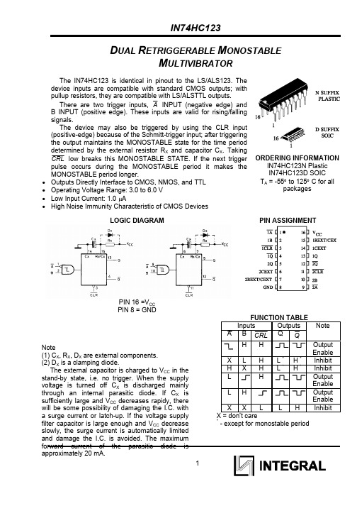
ORDERING INFORMATION IN74HC123N Plastic IN74HC123D SOIC TA = -55° to 125° C for all packages
PIN ASSIGNMENT
PIN 16 =VCC PIN 8 = GND FUNCTION TABLE Inputs Outputs Note A B CRL Q Q H H Output Enable X L H L* H* Inhibit * * H X H L H Inhibit L H Output Enable L H Output Enable X X L L H Inhibit X = don’t care * - except for monostable period
元器件交易网
IN74HC123
DUAL LE MONOSTABLE MULTIVIBRATOR
The IN74HC123 is identical in pinout to the LS/ALS123. The device inputs are compatible with standard CMOS outputs; with pullup resistors, they are compatible with LS/ALSTTL outputs. There are two trigger inputs, A INPUT (negative edge) and B INPUT (positive edge). These inputs are valid for rising/falling signals. The device may also be triggered by using the CLR input (positive-edge) because of the Schmitt-trigger input; after triggering the output maintains the MONOSTABLE state for the time period determined by the external resistor RX and capacitor CX. Taking CRL low breaks this MONOSTABLE STATE. If the next trigger pulse occurs during the MONOSTABLE period it makes the MONOSTABLE period longer. Outputs Directly Interface to CMOS, NMOS, and TTL Operating Voltage Range: 3.0 to 6.0 V Low Input Current: 1.0 µA High Noise Immunity Characteristic of CMOS Devices LOGIC DIAGRAM
74HC123中文资料
Product specification
74HC/HCT123
ORDERING INFORMATION
TYPE NUMBER
74HC123N; 74HCT123N 74HC123D; 74HCT123D 74HC123DB; 74HCT123DB 74HC123PW; 74HCT123PW
NAME DIP16
26 26 ns
nRD to nQ, nQ
REXT = 5 kΩ; CEXT = 0 pF
20
23
ns
CI
input capacitance
3.5 3.5 pF
CPD
power dissipation
capacitance per
notes 1 and 2 54 56 pF
monostable
Notes
An internal connection from nRD to the input gates makes it possible to trigger the circuit by a positive-going signal at input nRD as shown in the function table. Figures 7 and 8 illustrate pulse control by retriggering
2. For HC the condition is VI = GND to VCC For HCT the condition is VI = GND to VCC − 1.5 V
1998 Jul 08
2
元器件交易网
Philips Semiconductors
Dual retriggerable monostable multivibrator with reset
- 1、下载文档前请自行甄别文档内容的完整性,平台不提供额外的编辑、内容补充、找答案等附加服务。
- 2、"仅部分预览"的文档,不可在线预览部分如存在完整性等问题,可反馈申请退款(可完整预览的文档不适用该条件!)。
- 3、如文档侵犯您的权益,请联系客服反馈,我们会尽快为您处理(人工客服工作时间:9:00-18:30)。
HD74HC123ADual Retriggerable Monostable Multivibrators (with Clear)ADE-205-438 (Z)1st. EditionSep. 2000 DescriptionThis multivibrator features both a negative, A, and a positive, B, transition triggered input, either of which can be used as an inhibit input. Also included is a clear input that when taken low resets the one shot. The HD74HC123A can be triggered on the positive transition of the clear while A is held low and B is held high.The HD74HC123A is retriggerable. That is it may be triggered repeatedly while their outputs are generating a pulse and the pulse will be extended.Pulse width stability over a wide range of temperature. The output pulse equation is simply: t= (Rext)w (Cext).Features• High Speed Operation• High Output Current: Fanout of 10 LSTTL Loads• Wide Operating Voltage: V CC = 2 to 6 V• Low Input Current: 1 µA max• Low Quiescent Supply CurrentFunction TableInputs OutputsClear A B Q QL X X L HX H X L HX X L L HHD74HC123A Pin Arrangement2HD74HC123A3DC CharacteristicsSym-V CC Ta = 25°CTa = –40to +85°CItem bol (V)Min Typ Max Min Max Unit Test Conditions Input voltageV IH2.0 1.5—— 1.5—V4.5 3.15—— 3.15—6.04.2—— 4.2—V IL2.0——0.5—0.5V4.5—— 1.35— 1.356.0—— 1.8— 1.8Output voltageV OH2.0 1.9 2.0— 1.9—VVin = V IH or V IL I OH = –20 µA 4.5 4.4 4.5— 4.4—6.0 5.96.0— 5.9—4.5 4.18—— 4.13—I OH = –4 mA 6.05.68—— 5.63—I OH = –5.2 mAV OL2.0—0.00.1—0.1VVin = V IH or V IL I OL = 20 µA 4.5—0.00.1—0.16.0—0.00.1—0.14.5——0.26—0.33I OL = 4 mA 6.0——0.26—0.33I OL = 5.2 mAInput current Iin 6.0——±0.1—±1.0µA Vin = V CC or GND Quiescent Standby state I CC6.0——130—220µA Vin = V CC or Iout = 0 µA supply currentActive state——130—220GNDRext/Cext = 0.5 V CCHD74HC123A4AC Characteristics (C L = 50 pF, Input t r = t f = 6 ns)Ta = 25°CTa = –40 to +85°CItem SymbolV CC (V)Min Typ Max MinMax Unit Test Conditions Propagation delay t PLH2.0——210—265nsA, B or Clear to Qtime4.5—2242—536.0——36—45t PHL 2.0——240—300nsA, B or Clear to Q4.5—2348—606.0——41—51t PHL2.0——170—215nsClear to Q4.5—1834—436.0——29—37t PLH2.0——180—225nsClear to Q4.5—1636—456.0——31—38Output rise timet TLH2.0——75—95ns 4.5—515—196.0——13—16Output fall timet THL2.0——75—95ns 4.5—515—196.0——13—16Pulse widtht w2.0150——190—nsA, B, Clear4.5306—38—6.026——33—Minimum output t WQ(min)2.0— 1.5———µs Cext = 28 pFRext = 6 k Ωpulse width4.5—450———nsRext = 2 k Ω6.0—380———Output pulse width t WQ 4.5— 1.0———ms Cext = 0.1 µF, Rext = 10 k ΩInput capacitance Cin ——510—10pFCaution in use:In order to prevent any malfunctions due to noise, connect a high-frequency performance capacitor between V CC and GND, and keep the wiring between the External components and Cext, Rext/Cext pins as short as possible.HD74HC123A Package Dimensions5HD74HC123A6Cautions1.Hitachi neither warrants nor grants licenses of any rights of Hitachi’s or any third party’s patent,copyright, trademark, or other intellectual property rights for information contained in this document.Hitachi bears no responsibility for problems that may arise with third party’s rights, includingintellectual property rights, in connection with use of the information contained in this document.2.Products and product specifications may be subject to change without notice. Confirm that you have received the latest product standards or specifications before final design, purchase or use.3.Hitachi makes every attempt to ensure that its products are of high quality and reliability. However,contact Hitachi’s sales office before using the product in an application that demands especially high quality and reliability or where its failure or malfunction may directly threaten human life or cause risk of bodily injury, such as aerospace, aeronautics, nuclear power, combustion control, transportation,traffic, safety equipment or medical equipment for life support.4.Design your application so that the product is used within the ranges guaranteed by Hitachi particularly for maximum rating, operating supply voltage range, heat radiation characteristics, installationconditions and other characteristics. Hitachi bears no responsibility for failure or damage when used beyond the guaranteed ranges. Even within the guaranteed ranges, consider normally foreseeable failure rates or failure modes in semiconductor devices and employ systemic measures such as fail-safes, so that the equipment incorporating Hitachi product does not cause bodily injury, fire or other consequential damage due to operation of the Hitachi product.5.This product is not designed to be radiation resistant.6.No one is permitted to reproduce or duplicate, in any form, the whole or part of this document without written approval from Hitachi.7.Contact Hitachi’s sales office for any questions regarding this document or Hitachi semiconductor products.Hitachi, Ltd.Semiconductor & Integrated Circuits.Nippon Bldg., 2-6-2, Ohte-machi, Chiyoda-ku, Tokyo 100-0004, Japan Tel: Tokyo (03) 3270-2111 Fax: (03) 3270-5109Copyright © Hitachi, Ltd., 2000. All rights reserved. Printed in Japan.Hitachi Asia Ltd. Hitachi Tower16 Collyer Quay #20-00, Singapore 049318Tel : <65>-538-6533/538-8577 Fax : <65>-538-6933/538-3877URL : .sg URLNorthAmerica : /Europe : /hel/ecg Asia : Japan : http://www.hitachi.co.jp/Sicd/indx.htmHitachi Asia Ltd.(Taipei Branch Office)4/F, No. 167, Tun Hwa North Road, Hung-Kuo Building, Taipei (105), Taiwan Tel : <886>-(2)-2718-3666 Fax : <886>-(2)-2718-8180 Telex : 23222 HAS-TPURL : Hitachi Asia (Hong Kong) Ltd. Group III (Electronic Components) 7/F., North Tower, World Finance Centre,Harbour City, Canton Road Tsim Sha Tsui, Kowloon, Hong KongTel : <852>-(2)-735-9218 Fax : <852>-(2)-730-0281URL : Hitachi Europe Ltd.Electronic Components Group.Whitebrook ParkLower Cookham Road MaidenheadBerkshire SL6 8YA, United Kingdom Tel: <44> (1628) 585000Fax: <44> (1628) 585160Hitachi Europe GmbHElectronic Components Group Dornacher Stra βe 3D-85622 Feldkirchen, Munich GermanyTel: <49> (89) 9 9180-0Fax: <49> (89) 9 29 30 00Hitachi Semiconductor (America) Inc.179 East Tasman Drive,San Jose,CA 95134 Tel: <1> (408) 433-1990Fax: <1>(408) 433-0223For further information write to:Colophon 2.0。