MDM-25SBSP-TL61A174中文资料
Techno HDS系列数控路由器用户手册说明书

This manual will provide unpacking, maintenance, and user guide for running the Techno HDS Seriesand HDS Plus Series CNC Routers.It is suggested that the operator keep this manual by the machine. This will provide the most importantinformation pertaining to the operation of this machine.WARNING: DO NOT OPERATE THIS MACHINE WITHOUT PROPER TRAINING! Improper or unsafe operation of the machine will result in personal injury and/or damage to the equipment.1.3 Correct Colleting:Spindle Warm-up:1.3.6 —HSD Spindle WarmupRead these instructions thoroughly BEFORE operating machine.AND ADJUSTMENTPREHEATINGuses high-precision angular contact bearing pairs,pre-loaded and lubricatedgrease for high speeds.machine is switched on for the first time every day,allow the electrospindle preheating cycle in order to allow the bearings to gradually attain a uniform and hence to obtain a uniform expansion of the bearing races and thefollowing cycle is recommended,without machining operations:%of the maximum rated speed for2minutes.%of the maximum rated speed for2minutes.%of the maximum rated speed for1minute.preheating cycle should also be performed every time that the machine is inoperative the electrospindle to cool down to room temperature.for HSK versions:forbidden to run the electrospindle without the tool-holder inserted.While the machine is operating,the spindle can reach high temperatures.Be to touch it without due precautions.1.4.2All the electronics for the HDS machine are located in the housing cabinet. Do not open these doors when power is applied to the machine.1.4.3There are two rounded connectors on the side of the controller, these connectors provide 220 volts for the vacuum pump starter contactors.Lead the cable for 3 phase 220 volts that will be used to power machine through the hole on the bottom of the cabinet.220V in forpoweringmachine220V Outfor Vacuum PumpNetworkConnectionMotor/EncoderFig 1.4.3.Hole for mouse andkeyboard cableImproper electrical connections can result inFig 1.4.4.bFig 1.4.5 Should read90 psiFig 1.4.6starter. electronic unit.Attach the silver connectorfrom the starter box here. Attach the hoses from the machine to theT-connectors and attach them to the pump.Turn on individual sections of the vacuum table by turning the manifoldVacuum on and off functions are controlled by the Osai controllerand can only be turned on fromthe computer screen.To test the motor, press thereset button on the starter boxonce all connections are made.2432.1.2The red light on the front of the machine will light up. This indicates that 220 volts is coming into the machine.The Power ON light will light up Power OffPower ON E-stop: Turns off controller, motor and spindleUSB Port1243Press the Power ON button to start the system.Terminal192.168.0.1If the Boot Controller does not start after a minute and the message CNC is waiting for a BOOT mode directive appears on the screen, then normal mode needs to be selected.192.168.0.1The Axis not referenced error will appear.Click on “Home All” and all the axes will move to their home position. If any errors remain on the screen (i.e. Low Air Pressure,) rectify the problem and click on “Reset Errors” or “RESET” to remove the message.The machine is now ready to be jogged.Home AllReset ErrorsABC D E FGHJKLAFBC D EABCA - Home All:Sends the machine to the home position. (Absolute XYZ = 0). The Z axis will first move up to its limit, then the X and Y axes will move simultaneously.B - SINGLE AXIS HOME:When this button is left clicked, each axis can be homed separately. When the button is active, the user then clicks on the arrow key for the axis to be homed to enable the operation. [Ex: click single axis home, click X-, machine will home the x-axis only]C- CLEARANCE POSITION:A B C DA - Shroud Up/ Down:This button will raise or lower the dust shroud on the spindle.B - Pins Up / Down:This button will raise or lower the pop-up pins on the sides of the table.C - Vacuum 1 On/Off:This button will turn Vacuum 1 on and off, if it is connected. D - Vacuum 2 On/Off:This button will turn Vacuum 2 on and off, if it is connected.Shroud Up / Down and Pins Up / Down will only function if 90 lbs. of compressed air connected to the Vacuum 1 on/off and Vacuum 2 on/off send 220 volts to the starter coil of the vacuum pump, thus DownUpDown UpABCA - Offsets:Opens the Offset Menu. In this menu the user can save multiple offsets/originsand apply them to the coordinate system.B - I/O:Opens the Input and Output screen diagnostics. These screens will show thestates of the inputs and outputs.C - Tool:Opens the Tool Menu. In this menu the user can store tool lengths and changetool numbers.ABCDA - XYZ Coordinates:This displays the location of the machine. If the Origin No is zero,the numbers displayed are the distance from the Home position (Absolute XYZ = 0). If there is an Origin Number active, the numbers displayed are the distance from that origins zero position.B - Tool:This displays the tool that is currently in the spindle. If the number reads a single digit then there is no offset applied to that tool at this time. When the Tool displays 1.1, or 2.2, or 5.5 etc then the Z-offset is active. The Z-offset needs to be active when setting the origin.C - Origin No:This displays the active origin/ coordinate system. When it reads 0, no origin is active and the coordinate system displayed is the from the Home position. The system is setup to accommodate 8 origins, but many more can be made available.A B CA BC DEFG HBAA-Spindle On/Off :If you press the button beside the ON switch, you will turn the spindle on. If you press the button beside the OFF switch, you will turn the spindle off.B-AUX (Coolant) On/Off :Pressing the button beside On will turn the AUX (coolant) on, pressing the button beside Off will turn the AUX (coolant) off (it will do nothing if the system does not have a coolant).I-Load G-Code FileAA B C DE F GHI JA B C DE FGHA - Tool Offset Preset:This section allows the user to manually enter tool offsets.B - CHANGE TOOL:Left clicking on one of these buttons will make the machine pick up the corresponding tool number.C - IDENTIFY TOOL:Left clicking on one of these buttons will change the tool number on the screen and apply the Z-Offset to that specific tool D - Jog Functions:This is a minimized version of the regular jog functions.E - Z-Offset Update:Pressing one of these buttons will cause the Tool to move down until it touches the Tool Calibration Block, and then it will store the Z-offset for that tool number.F - Pneumatic Controls:This section controls dust shroud, chuck control and pop up pins.G - HOLD:IJ KABC D EFGHClick on the box beside the mode name toselect it.Increase (+) or decrease (-) the Jog Speed by pressing the (+) or (-) box. Speed is shown in % of maximum speed. Actual speed is displayed when the machine is running. Increase or decrease the Jog Step by pressing the (+) or (-) box. Step size in inches will be shown.When this mode is selected a Test box will appear.G-code commands can be entered in this box, then clicking Cycle Start will run the command. Eg,G0 X10Y10 in the box then Cycle start will move the machine to X10 Y10M3 S18000 will turn on the spindle at a speed of 18000rpmM5 will turn off the spindle.(UAO,03) will activate Origin 3-Click Reset to remove any offsets.-Click OFST # . Where # is the number of the Tool you have in the chuck.The machine will go to Top of the Z travel, then slowly move down to the pad. It will touch the brass colored section of the pad, retract, and then move down again to confirm the value. Repeat this procedure for the other tools.Tool Lengths are now learned. Press “RESET” to remove Blue Notification Warning take note of the T.OFFSET3To set the Origin:Move the machine to the location on the table you want to set as XYZ. Use the handwheel for precision.XYZ zero position is the location point on a drawing in a CAD/CAM package where X,Y and Z all equal zero. Generally, XY zero is on the bottom left corner and Z zero is the top of the part. The letters to be cut are located away from the XY zero.Once in position switch to Continuous Jog Continuous must be active to save origin.1 023 Locate the File you want to load.Left click on the file.Manual Setup will allow the user to change the Jog step size.Checking Auto will mean the machine will jog the full step size when the jog arrow is pressed once. Checking Manual will mean the machine will only jog while the arrow is held down. When it reaches the step size, it will stop and the user will have to release the button and press again.All the other options on this window are disabled.Click on Browse and pick / create a suitable folder to save the backup, enter a suitable file name for the backup and click Save.To Restore a saved backup, just reboot in setup mode again, and select Restore to load the saved settings.Y axisX axisZ axis(Diagram 2. The current aggregate angle.)(Diagram 3. Loosen these screws to adjust the aggregate angle.)Diagram 1 illustrates how the aggregate must be seated in the ISO30 tool clip.Diagrams 2 and 3 illustrate how to adjust the angle of the aggregate cutting tools. It is essential that the pin (shown in Diagram 1) remains in the shown position so that it aligns with the aggregate tool ring and ISO30 tool clip.1312Wipe the linear rails and bearings once a day to assure smooth play free motion.Lubricate the rack and pinion and the ball screw drive once every week so as to ensure longer service life.When lubricating the z-axis screw,recommended to use Kluber TA 15/2 or PETAMOGY 193 or equivalent.Caution:Switch off the main power supply before servicing. If power supply needed, qualified personnel shall operate it.Clean the cabinet with dust collector once every week. Be careful not to damage or loosen any wire connections. Compressed air may be used but from at least 4 foot distance.Check the fan filters every month. Clean and / or replace if necessary.。
74271112S;中文规格书,Datasheet资料
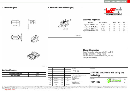
7.1 7.0 6.02012-06-272012-04-302008-01-03SStSStSMuSStSMu-Würth Elektronik eiSos GmbH & Co. KGEMC & Inductive SolutionsMax-Eyth-Str. 174638 WaldenburgGermanyTel. +49 (0) 79 42 945 - 0A Dimensions: [mm] Additional FeaturesSafety key to lock/ unkock STAR-CLIP Fixation74271 7427711D2 General Properties:Ferrite core Ferrite core Ferrite core Plastic housing Plastic housing Test cable Test cablePropertiesMaterial Initial permeability Curie temperatureColourFlammability ClassificationApplicable cable Applicable cable lengthµi T CValue 4 W 620620150Black UL94-V0AWG2690Unit°Cmm Tol.typ.typ.F Typical Impedance Characteristics:I Cautions and Warnings:The following conditions apply to all goods within the product series of WE-STAR TECof Würth Elektronik eiSos GmbH & Co. KG:General:All recommendations according to the general technical specifications of the data sheet have to be complied with.The disposal and operation of the product within ambient conditions which probably alloy or harm the component surface has to be avoided.The packaging of the product is to encase the needed humidity of the plastic housing. To ensure the humidity level, the products have to be stored in this delivered packaging. If not, the products are losing their humidity. In this case you can re-condition the components according to the internal standard WE1883 to ensure the necessary humidity in the plastic.To ensure the operating mode of the product, the ambient temperature at processing (when the part will be mounted on the cable) has to be in the range of 15 to 25 °C.Before mounting, the part should be stored for one hour in this condition.The responsibility for the applicability of customer specific products and the use in a particular customer design is always within the authority of the customer. All technical specifications for standard products do also apply for customer specific products.Direct mechanical impact to the product and the forcible closing of this shall be prevented as the ferrite material of the ferrite body or the pla-stic housing could flake or in the worst case it could break.Product specific:Follow all instructions mentioned in the datasheet, especially:•The cable diameter must be pointed out, otherwise no warranty will be sustained.•Violation of the technical product specifications such as exceeding the nominal rated current will result in the loss of warranty.1. General Customer ResponsibilitySome goods within the product range of Würth Elektronik eiSos GmbH & Co. KG contain statements regarding general suitability for certain application areas. These statements about suitability are based on our knowledge and experience of typical requirements concerning the are-as, serve as general guidance and cannot be estimated as binding statements about the suitability for a customer application. The responsibi-lity for the applicability and use in a particular customer design is always solely within the authority of the customer. Due to this fact it is up to the customer to evaluate, where appropriate to investigate and decide whether the device with the specific product characteristics described in the product specification is valid and suitable for the respective customer application or not.2. Customer Responsibility related to Specific, in particular Safety-Relevant ApplicationsIt has to be clearly pointed out that the possibility of a malfunction of electronic components or failure before the end of the usual lifetime can-not be completely eliminated in the current state of the art, even if the products are operated within the range of the specifications.In certain customer applications requiring a very high level of safety and especially in customer applications in which the malfunction or failure of an electronic component could endanger human life or health it must be ensured by most advanced technological aid of suitable design of the customer application that no injury or damage is caused to third parties in the event of malfunction or failure of an electronic component.3. Best Care and AttentionAny product-specific notes, warnings and cautions must be strictly observed.4. Customer Support for Product SpecificationsSome products within the product range may contain substances which are subject to restrictions in certain jurisdictions in order to serve spe-cific technical requirements. Necessary information is available on request. In this case the field sales engineer or the internal sales person in charge should be contacted who will be happy to support in this matter.5. Product R&DDue to constant product improvement product specifications may change from time to time. As a standard reporting procedure of the Product Change Notification (PCN) according to the JEDEC-Standard inform about minor and major changes. In case of further queries regarding the PCN, the field sales engineer or the internal sales person in charge should be contacted. The basic responsibility of the customer as per Secti-on 1 and 2 remains unaffected.6. Product Life CycleDue to technical progress and economical evaluation we also reserve the right to discontinue production and delivery of products. As a stan-dard reporting procedure of the Product Termination Notification (PTN) according to the JEDEC-Standard we will inform at an early stage about inevitable product discontinuance. According to this we cannot guarantee that all products within our product range will always be available. Therefore it needs to be verified with the field sales engineer or the internal sales person in charge about the current product availability ex-pectancy before or when the product for application design-in disposal is considered.The approach named above does not apply in the case of individual agreements deviating from the foregoing for customer-specific products.7. Property RightsAll the rights for contractual products produced by Würth Elektronik eiSos GmbH & Co. KG on the basis of ideas, development contracts as well as models or templates that are subject to copyright, patent or commercial protection supplied to the customer will remain with Würth Elektronik eiSos GmbH & Co. KG.8. General Terms and ConditionsUnless otherwise agreed in individual contracts, all orders are subject to the current version of the “General Terms and Conditions of Würth Elektronik eiSos Group”, last version available at .J Important Notes:The following conditions apply to all goods within the product range of Würth Elektronik eiSos GmbH & Co. KG:分销商库存信息: WURTH-ELECTRONICS 74271112S。
Modicon M241 产品数据手册说明书

i s c l a im e r : T h i s d o c u m e n t a t i o n i s n o t i n t e n d e d a s a s u b s t i t u t e f o r a n d i s n o t t o b e u s e d f o r d e t e r m i n i n g s u i t a b i l i t y o r r e l i a b i l i t y o f t h e s e p r o d u c t s f o r s p e c i f i c u s e r a p p l i c a t i o n sProduct datasheetCharacteristicsTM241CE40Tcontroller M241 40 IO transistor PNP EthernetMainRange of productModicon M241Product or component type Logic controller [Us] rated supply voltage 24 V DCDiscrete input number 24 discrete input including 8 fast input conforming to IEC 61131-2 Type 1Discrete output type TransistorDiscrete output number 16 transistor including 4 fast output Discrete output voltage 24 V DC for transistor outputDiscrete output current0.1 A with Q0...Q3 terminal(s) for fast output (PTO mode)0.5 A with Q0...Q15 terminal(s) for transistor outputComplementaryDiscrete I/O number40Number of I/O expansion module 7 (local I/O architecture)14 (remote I/O architecture)Supply voltage limits 20.4...28.8 V Inrush current<= 50 APower consumption in W 32.6...40.4 W with max number of I/O expansion module Discrete input logic Sink or source Discrete input voltage 24 V Discrete input voltage type DCVoltage state1 guaranteed >= 15 V for input Current state 1 guaranteed >= 2.5 mA for input >= 5 mA for fast input Voltage state 0 guaranteed <= 5 V for input Current state 0 guaranteed <= 1 mA for input<= 1.5 mA for fast input Discrete input current 7 mA for input10.7 mA for fast input Input impedance4.7 kOhm for input2.81 kOhm for fast inputResponse time<= 2 µs turn-on operation with I0...I7 terminal(s) for fast input<= 2 µs turn-off operation with I0...I7 terminal(s) for fast input<= 2 µs turn-on operation with Q0...Q3 terminal(s) for fast output<= 2 µs turn-off operation with Q0...Q3 terminal(s) for fast output50 µs turn-on operation with I0...I15 terminal(s) for input50 µs turn-off operation with I0...I15 terminal(s) for input<= 34 µs turn-on operation with Q0...Q15 terminal(s) for output<= 250 µs turn-off operation with Q0...Q15 terminal(s) for outputConfigurable filtering time 1 µs for fast input12 ms for fast input0 ms for input1 ms for input4 ms for input12 ms for inputDiscrete output logic Positive logic (source)Output voltage limits30 V DCCurrent per output common 2 AOutput frequency<= 20 kHz for fast output (PWM mode)<= 100 kHz for fast output (PLS mode)<= 1 kHz for outputAccuracy+/- 0.1 % at 20...100 Hz for fast output+/- 1 % at 100 Hz...1 kHz for fast outputLeakage current<= 5 µA for outputVoltage drop<= 1 VTungsten load<= 2.4 WProtection type Short-circuit and overload protection with automatic resetReverse polarity protection for fast outputShort-circuit protectionReset time10 ms automatic reset output12 s automatic reset fast outputMemory capacity8 MB for program64 MB for system memory RAMData backed up128 MB built-in flash memory for backup of user programsData storage equipment<= 32 GB SD card optionalBattery type BR2032 lithium non-rechargeable, battery life: 4 yrBackup time 2 years at 25 °CExecution time for 1 KInstruction0.3 ms for event and periodic task0.7 ms for other instructionApplication structure8 external event tasks4 cyclic master tasks3 cyclic master tasks + 1 freewheeling task8 event tasksRealtime clock WithClock drift<= 60 s/month at 25 °CPositioning functions PWM/PTO function 4 channel(s) (positioning frequency: 100 kHz)Counting input number 4 fast input (HSC mode)Control signal type A/B signal at 100 kHz for fast input (HSC mode)Pulse/Direction signal at 200 kHz for fast input (HSC mode)Single phase signal at 200 kHz for fast input (HSC mode)Integrated connection type USB port with connector mini B USB 2.0Ethernet with connector RJ45Non isolated serial link "serial 1" with connector RJ45 and interface RS232/RS485Non isolated serial link "serial 2" with connector removable screw terminal block and interface RS485 Supply Serial link supply "serial 1" at 5 V, 200 mATransmission rate 1.2...115.2 kbit/s (115.2 kbit/s by default) for bus length of 15 m - communication protocol: RS4851.2...115.2 kbit/s (115.2 kbit/s by default) for bus length of 3 m - communication protocol: RS232480 Mbit/s for bus length of 3 m - communication protocol: USB10/100 Mbit/s - communication protocol: EthernetCommunication port protocol Modbus non isolated serial link with master/slave methodPort Ethernet 1 - 10BASE-T/100BASE-TX port with copper cable supportCommunication service FDRDownloadingIEC VAR ACCESSMonitoringNGVLProgrammingUpdating firmwareSMS notificationsDHCP server (via TM4 Ethernet switch network module)DHCP client (embedded Ethernet port)SNMP client/serverFTP client/serverSQL clientSend email from the controller based on TCP/UDP libraryModbus TCP client I/O scannerEthernet/IP originator I/O scanner (embedded Ethernet port)Ethernet/IP target, Modbus TCP server and Modbus TCP slaveLocal signalling 1 LED green for SD card access (SD)1 LED red for BAT1 LED green for SL11 LED green for SL21 LED per channel green for I/O state1 LED red for I/O error (I/O)1 LED red for bus fault on TM4 (TM4)1 LED green for Ethernet port activity1 LED red for module error (ERR)1 LED green for PWR1 LED green for RUNElectrical connection Removable screw terminal block for inputs and outputs (pitch 5.08 mm)Removable screw terminal block for connecting the 24 V DC power supply (pitch 5.08 mm) Cable length<= 50 m unshielded cable for input<= 10 m shielded cable for fast input<= 3 m shielded cable for fast output<= 50 m unshielded cable for outputInsulation500 V AC between fast input and internal logicNon-insulated between inputs500 V AC between output and internal logic500 V AC between fast output and internal logicNon-insulated between outputs500 V AC between input and internal logic500 V AC between output groups500 V AC between supply and internal logicNon-insulated between supply and groundMarking CESurge withstand 1 kV for power lines (DC) in common mode conforming to EN/IEC 61000-4-51 kV for shielded cable in common mode conforming to EN/IEC 61000-4-50.5 kV for power lines (DC) in differential mode conforming to EN/IEC 61000-4-51 kV for relay output in differential mode conforming to EN/IEC 61000-4-51 kV for input in common mode conforming to EN/IEC 61000-4-51 kV for transistor output in common mode conforming to EN/IEC 61000-4-5Web services Web serverMaximum number of connections8 connection(s) for Modbus server8 connection(s) for SoMachine protocol10 connection(s) for web server4 connection(s) for FTP server16 connection(s) for Ethernet/IP target8 connection(s) for Modbus clientNumber of slave16 Ethernet/IP64 Modbus TCPCycle time10 ms 16 Ethernet/IP64 ms 64 Modbus TCPMounting support Top hat type TH35-15 rail conforming to IEC 60715Top hat type TH35-7.5 rail conforming to IEC 60715Plate or panel with fixing kitHeight90 mmDepth95 mmWidth190 mmProduct weight0.62 kgEnvironmentStandards CSA C22.2 No 142ANSI/ISA 12-12-01UL 1604CSA C22.2 No 213EN/IEC 61131-2 : 2007Marine specification (LR, ABS, DNV, GL)UL 508Product certificationsCSA cULus RCMIACS E10Resistance to electrostatic discharge 4 kV on contact conforming to EN/IEC 61000-4-28 kV in air conforming to EN/IEC 61000-4-2Resistance to electromagnetic fields10 V/m (80 MHz...1 GHz) conforming to EN/IEC 61000-4-33 V/m (1.4 GHz...2 GHz) conforming to EN/IEC 61000-4-31 V/m (2 GHz...3 GHz) conforming to EN/IEC 61000-4-3Resistance to fast transients2 kV for power lines conforming to EN/IEC 61000-4-41 kV for Ethernet line conforming to EN/IEC 61000-4-41 kV for serial link conforming to EN/IEC 61000-4-41 kV for input conforming to EN/IEC 61000-4-41 kV for transistor output conforming to EN/IEC 61000-4-4Resistance to conducted disturbances,induced by radio frequency fields10 V (0.15...80 MHz) conforming to EN/IEC 61000-4-63 V (0.1...80 MHz) conforming to Marine specification (LR, ABS, DNV, GL)10 V (spot frequency (2, 3, 4, 6.2, 8.2, 12.6, 16.5, 18.8, 22, 25 MHz)) conforming to Marine specification (LR, ABS, DNV, GL)Electromagnetic emissionConducted emissions, test level: 120...69 dBµV/m QP, condition of test: power lines (radio frequency:10...150 kHz) conforming to EN/IEC 55011Conducted emissions, test level: 79...63 dBμV/m QP, condition of test: power lines (radio frequency:150 kHz...1.5 MHz) conforming to EN/IEC 55011Conducted emissions, test level: 63 dBμV/m QP, condition of test: power lines (radio frequency:1.5...30 MHz) conforming to EN/IEC 55011Radiated emissions, test level: 40 dBμV/m QP with class A (radio frequency: 30...230 MHz)conforming to EN/IEC 55011Radiated emissions, test level: 47 dBμV/m QP with class A (radio frequency: 230 MHz...1 GHz)conforming to EN/IEC 55011Immunity to microbreaks10 msAmbient air temperature for operation -10...55 °C for horizontal installation -10...50 °C for vertical installation Ambient air temperature for storage -25...70 °CRelative humidity 10...95 % without condensation in operation 10...95 % without condensation in storage IP degree of protection IP20 with protective cover in place Pollution degree 2Operating altitude 0...2000 m Storage altitude 0...3000 mVibration resistance3.5 mm (vibration frequency: 5...8.4 Hz) on symmetrical rail 3 gn (vibration frequency: 8.4...150 Hz) on symmetrical rail 3.5 mm (vibration frequency:5...8.4 Hz) on panel mounting 3 gn (vibration frequency: 8.4...150 Hz) on panel mounting Shock resistance15 gn for 11 msOffer SustainabilitySustainable offer status Green Premium productRoHS (date code: YYWW)Compliant - since 1330 - Schneider Electric declaration of conformity Schneider Electric declaration of conformity REAChReference not containing SVHC above the threshold Reference not containing SVHC above the threshold Product environmental profileAvailableProduct environmental Product end of life instructionsAvailableEnd of life manualDimensions Drawings DimensionsClearanceMounting PositionAcceptable MountingNOTE: Expansion modules must be mounted above the logic controller.Incorrect MountingDirect Mounting On a Panel Surface Mounting Hole LayoutDigital InputsWiring Diagram(*) :Type T fuse(1) :The COM0, COM1 and COM2 terminals are not connected internally (A) :Sink wiring (positive logic)(B) :Source wiring (negative logic)Fast Input Wiring (I0...I7)Fast Transistor OutputsWiring Diagram(*) :Type T fuse(1)The V0+, V1+, V2+ and V3+ terminals are not connected internally.(2)The V0-, V1-, V2- and V3- terminals are not connected internally.Transistor OutputsWiring Diagram(*) :Type T fuse(1) :The V1+, V2+ and V3+ terminals are not connected internally.(2) :The V1–, V2– and V3– terminals are not connected internally.USB Mini-B ConnectionEthernet Connection to a PC。
高科特实际产品说明书
4
Specifications are subject to change without notice (21.06.2021)
Solid State Relays Accessories, Screw Kits Types SRWKIT…
Ordering Key
Screw Kit Screw size Screw length
0.5 Nm -20° to + 70°C [-4 to +158°F] -40° to + 100°C [-40° to +212°F] DIN EN 50022, 50035
DIN Adaptor for 1-phase SSRs
DIN rail adaptor module for mounting the 1-phase SSR series RA, RD, RM, RS and RAM directly on DIN rail.
Type
UL style 2547 UL style 2464 UL style 2464 UL style 2464 UL style 2464 UL style 2464
Cable size
0.14mm2 0.14mm2 0.14mm2 0.25mm2 0.14mm2 0.14mm2
Termination
- Width x Height x Thickness = 35 x 43 x 0.25 mm
- Packing qty. 50 pcs.
RZHT
- Graphite thermal pad for RZ3 series with adhesive on one side
- Width x Height x Thickness = 70 x 77 x 0.25 mm
微专米 G.Fast 双频通道线驱动器数据表说明书
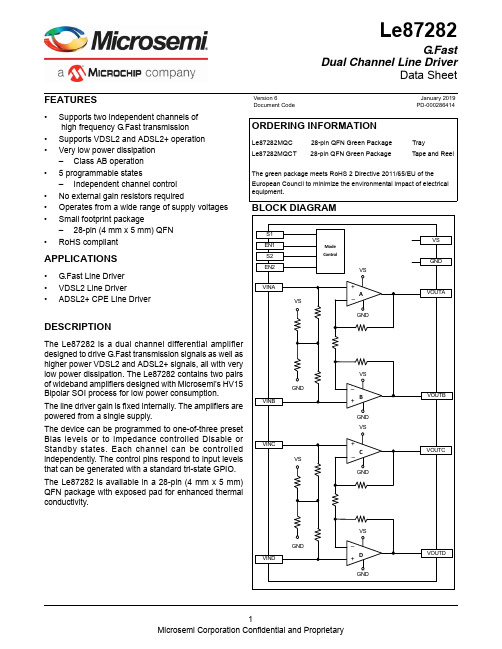
Le87282G.FastDual Channel Line DriverData Sheet FEATURES•Supports two independent channels ofhigh frequency G.Fast transmission•Supports VDSL2 and ADSL2+ operation•Very low power dissipation–Class AB operation• 5 programmable states–Independent channel control•No external gain resistors required•Operates from a wide range of supply voltages•Small footprint package–28-pin (4 mm x 5 mm) QFN•RoHS compliantAPPLICATIONS•G.Fast Line Driver•VDSL2 Line Driver•ADSL2+ CPE Line DriverDESCRIPTIONThe Le87282 is a dual channel differential amplifierdesigned to drive G.Fast transmission signals as well ashigher power VDSL2 and ADSL2+ signals, all with verylow power dissipation. The Le87282 contains two pairsof wideband amplifiers designed with Microsemi’s HV15Bipolar SOI process for low power consumption.The line driver gain is fixed internally. The amplifiers arepowered from a single supply.The device can be programmed to one-of-three presetBias levels or to impedance controlled Disable orStandby states. Each channel can be controlledindependently. The control pins respond to input levelsthat can be generated with a standard tri-state GPIO.The Le87282 is available in a 28-pin (4 mm x 5 mm)QFN package with exposed pad for enhanced thermalconductivity.ORDERING INFORMATIONLe87282MQC 28-pin QFN Green Package TrayLe87282MQCT 28-pin QFN Green Package Tape and ReelThe green package meets RoHS2 Directive2011/65/EU of theEuropean Council to minimize the environmental impact of electricalequipment.Version 6 January 2019Document Code PD-000286414TABLE OF CONTENTSFeatures. . . . . . . . . . . . . . . . . . . . . . . . . . . . . . . . . . . . . . . . . . . . . . . . . . . . . . . . . . . . . . . . . . . . . . . . . .1 Applications . . . . . . . . . . . . . . . . . . . . . . . . . . . . . . . . . . . . . . . . . . . . . . . . . . . . . . . . . . . . . . . . . . . . . . .1 Description . . . . . . . . . . . . . . . . . . . . . . . . . . . . . . . . . . . . . . . . . . . . . . . . . . . . . . . . . . . . . . . . . . . . . . . .1 Ordering Information. . . . . . . . . . . . . . . . . . . . . . . . . . . . . . . . . . . . . . . . . . . . . . . . . . . . . . . . . . . . . . . . .1 Block Diagram . . . . . . . . . . . . . . . . . . . . . . . . . . . . . . . . . . . . . . . . . . . . . . . . . . . . . . . . . . . . . . . . . . . . .1 Connection Diagram. . . . . . . . . . . . . . . . . . . . . . . . . . . . . . . . . . . . . . . . . . . . . . . . . . . . . . . . . . . . . . . . .3 Pin Descriptions . . . . . . . . . . . . . . . . . . . . . . . . . . . . . . . . . . . . . . . . . . . . . . . . . . . . . . . . . . . . . . . . . . . .4 Absolute Maximum Ratings . . . . . . . . . . . . . . . . . . . . . . . . . . . . . . . . . . . . . . . . . . . . . . . . . . . . . . . . . . .5 Thermal Resistance . . . . . . . . . . . . . . . . . . . . . . . . . . . . . . . . . . . . . . . . . . . . . . . . . . . . . . . . . . . .5 Package Assembly. . . . . . . . . . . . . . . . . . . . . . . . . . . . . . . . . . . . . . . . . . . . . . . . . . . . . . . . . . . . .5 Operating Ranges . . . . . . . . . . . . . . . . . . . . . . . . . . . . . . . . . . . . . . . . . . . . . . . . . . . . . . . . . . . . . . . . . .5 Device Specifications. . . . . . . . . . . . . . . . . . . . . . . . . . . . . . . . . . . . . . . . . . . . . . . . . . . . . . . . . . . . . . . .6 State Control. . . . . . . . . . . . . . . . . . . . . . . . . . . . . . . . . . . . . . . . . . . . . . . . . . . . . . . . . . . . . . . . . . . . . . .7 Applications . . . . . . . . . . . . . . . . . . . . . . . . . . . . . . . . . . . . . . . . . . . . . . . . . . . . . . . . . . . . . . . . . . . . . . .7 Line Driver Protection. . . . . . . . . . . . . . . . . . . . . . . . . . . . . . . . . . . . . . . . . . . . . . . . . . . . . . . . . . .8 Physical Dimensions . . . . . . . . . . . . . . . . . . . . . . . . . . . . . . . . . . . . . . . . . . . . . . . . . . . . . . . . . . . . . . . .9 28-pin QFN . . . . . . . . . . . . . . . . . . . . . . . . . . . . . . . . . . . . . . . . . . . . . . . . . . . . . . . . . . . . . . . . . .9CONNECTION DIAGRAMNote:1.Pin 1 is marked for orientation.2.The Le87282 device incorporates an exposed die pad on the underside of its package. The pad acts as a heat sink and must be connectedto a copper plane through thermal vias, for proper heat dissipation. It is electrically isolated and maybe connected to GND.PIN DESCRIPTIONSPin #Pin Name Type Description1IREF Input Device internal reference current. Connect a resistor (R REF ) to GND.2VINA Input Non-inverting input of amplifier A 3VINB Input Non-inverting input of amplifier B 4GND Ground Reference ground5GND 6VINC Input Non-inverting input of amplifier C 7VIND InputNon-inverting input of amplifier D 8NC No internal connection 9S2Input Channel 2 state control 10VOUTD Output Amplifier D output11EN2Input Enable Channel 2 transmission 12VOUTC Output Amplifier C output13NC No internal connection14NC 15NC 16NC 17GND GroundReference ground 18VS PowerPower Supply19VS 20VS 21GND GroundReference ground22NC No internal connection23NC 24NC 25VOUTB Output Amplifier B output26EN1Input Enable Channel 1 transmission 27VOUTA Output Amplifier A output 28S1InputChannel 1 state controlExposed padElectrically isolated thermal conduction pad, can be groundedABSOLUTE MAXIMUM RATINGSStresses above the values listed under Absolute Maximum Ratings can cause permanent device failure.Functionality at or above these limits is not implied. Exposure to absolute maximum ratings for extended periods can affect device reliability .Notes:1.Continuous operation above 145°C junction temperature may degrade device reliability.2.See Thermal Resistance .3.No air flow.Thermal ResistanceThe thermal performance of a thermally enhanced package is assured through optimized printed circuit board layout.Specified performance requires that the exposed thermal pad be soldered to an equally sized exposed copper surface, which, in turn, conducts heat through multiple vias to larger internal copper planes.Package AssemblyThe green package devices are assembled with enhanced, environmental compatible lead-free, halogen-free, and antimony-free materials. The leads possess a matte-tin plating which is compatible with conventional board assembly processes or newer lead-free board assembly processes.Refer to IPC/JEDEC J-Std-020 Table 4 for recommended peak soldering temperature and Table 5-2 for the recommended solder reflow temperature profile.OPERATING RANGESMicrosemi guarantees the performance of this device over the industrial (-40°C to 85°C) temperature range by conducting electrical characterization over each range and by conducting a production test with single insertion coupled with periodic sampling. These characterization and test procedures comply with the Telcordia GR-357-CORE Generic Requirements for Assuring the Reliability of Components Used in Telecommunications Equipment.Storage Temperature-65 ≤ T A ≤ +150°C Operating Junction Temperature (Note 1)-40 ≤ T j ≤ +150°C VS with respect to GND-0.3 V to +16 V Control inputs with respect to GND -0.3 V to 4 V Continuous Driver Output Current100 mA Maximum device power dissipation, continuous (2) - T A = 85°C, P D 1.7W Junction to ambient thermal resistance (2,3), θJA 36.0°C/W Junction to board thermal resistance (2), θJB18.3°C/W Junction to case bottom (exposed pad) thermal resistance, θJC (BOTTOM)8.9°C/W Junction-to-top characterization parameter (2), ψJT 1.2°C/WESD Immunity (Human Body Model)JESD22 Class 2 compliant ESD Immunity (Charge Device Model)JESD22 Class IV compliantAmbient temperature T A-40°C to +85°C Power SupplyVS with respect to GND:Typical usage+8V to +15V,+12V ± 5%DEVICE SPECIFICATIONSTypical Conditions: As shown in the basic test circuit (Figure 1) with VS = +12 V, R REF = 75 k Ω, and T A = 25°C.Min/Max Parameters: T A = -40 to +85°C.Figure 1.Basic Test Circuit - Channel 1 ShownTable 1.Electrical SpecificationsSymbolParameter Description ConditionMinTyp Max Unit NotesSupply Characteristics P VS Supply Power (per channel)Transmission, P LINE = 4 dBm 470600mW Receive period, Disable state 175250mW I VSSupply Current (per channel)Standby State11.5mAControl Input (S1, S2, EN1, EN2 ) Specifications V IH Input High Voltage 2.03.3 3.6V V IM Input Middle Voltage 1.5V V ILInput Low Voltage -0.300.8V Enable Time 500ns Disable TimeDisable state500nsAmplifier CharacteristicsDifferential Gain VOUT/VIN 18.318.819.1dB Gain Flatness2 − 106 MHz-1.51dB 1V O Output Voltage 10V I O Output Current 150mA 1Z I Input Impedance Differential 131518k ΩZ O Output Impedance Disable state 60ΩAmplifier Dynamic CharacteristicsNoise Input Referred Noise 2 - 106 MHz915nV/1TSDThermal Shutdown Temperature170°CNotes: 1. Not tested in production. Guaranteed by characterization and design.HzSTATE CONTROLS1, EN1 and S2, EN2 pins are used as combinatorial logic inputs to control the line driver operating states. Table 2 and Table 3 show the programmable states for each channel.S1, EN1 and S2, EN2 are tri-state inputs that accept three operating levels. These pins have internal resistors tied to +1.5 V which force a middle logic input level when the control to these pins is tri-stated.Table 2.Channel 1 Control MatrixS1EN1State ApplicationX0DisableX Open Standby01Enable Low Bias ADSL2+Open1Enable Medium Bias VDSL211Enable Full Bias G.FastTable 3.Channel 2 Control MatrixS2EN2State ApplicationX0DisableX Open Standby01Enable Low Bias ADSL2+Open1Enable Medium Bias VDSL211Enable Full Bias G.FastDisable State: Amplifier output = VS/2. The Disable state should be used during the receive period. The device presents a controlled low impedance to the line during this state.Standby State: Amplifier bias current removed. This is the lowest power state. Amplifier output is high impedance. Gain-setting feedback resistors are still connected across amplifier output pins, creating 1300ohm differential impedance at pins.Bias States: Line Driver is active for transmission. States are different only in the amount of bias current to the amplifiers, and therefore power consumption. There is a trade-off between bias current and bandwidth. APPLICATIONSThe Le87282 integrates two sets of high-power line driver amplifiers that can be connected for half-duplex differential line transmissions. The amplifiers are designed to be used with signals up to 106 MHz with low signal distortion. The Le87282 can be used for G.Fast applications as illustrated in Figure 2, or it can be used for VDSL2 or ADSL2+ applications. For VDSL2 or ADSL2+ applications, the output resistor values need to be reduced in order to achieve the desired load power of these applications.Figure 2 shows a G.Fast application circuit with amplifiers A and B in transmission and amplifiers C and D in the receive period (Disable state). Amplifiers C and D drive 0 ohms in the Disable state.Figure 2.Typical G.Fast Application CircuitInput ConsiderationsThe driving source impedance should be less than 100 nH to avoid any ringing or oscillation.Output Driving ConsiderationsThe internal metallization is designed to carry up to about 100 mA of steady DC current and there is no current limit mechanism. The device does feature integrated thermal shutdown protection however with hysteresis. Driving lines with no series resistor is not recommended.Power Supplies and Component PlacementThe power supplies should be well bypassed close to the Le87282 device. A 2.2 µF tantalum capacitor and a 0.1 µF ceramic capacitor for the VS supply is recommended.Line Driver ProtectionHigh voltage transients such as lightning can appear on the telephone lines. Transient protection devices should be used to absorb the transient energy and clamp the transient voltages. The series output termination resistors limit the current going into the line driver and internal clamps. The protection scheme depends on the type of data transformer used and the line protection components used in the front of the data transformer.PHYSICAL DIMENSIONSNote:Packages may have mold tooling markings on the surface. These markings have no impact on the form, fit or function of the de-vice. Markings will vary with the mold tool used in manufacturing.Information relating to products and services furnished herein by Microsemi Corporation or its subsidiaries (collectively “Microsemi”) is believed to be reliable. However, Microsemi assumes no liability for errors that may appear in this publication, or for liability otherwise arising from the application or use of any such information, product or service or for any infringement of patents or other intellectual property rights owned by third parties which may result from such application or use. Neither the supply of such information or purchase of product or service conveys any license, either express or implied, under patents or other intellectual property rights owned by Microsemi or licensed from third parties by Microsemi, whatsoever. Purchasers of products are also hereby notified that the use of product in certain ways or in combination with Microsemi, or non-Microsemi furnished goods or services may infringe patents or other intellectual property rights owned by Microsemi.This publication is issued to provide information only and (unless agreed by Microsemi in writing) may not be used, applied or reproduced for any purpose nor form part of any order or contract nor to be regarded as a representation relating to the products or services concerned. The products, their specifications, services and other information appearing in this publication are subject to change by Microsemi without notice. No warranty or guarantee express or implied is made regarding the capability, performance or suitability of any product or service. Information concerning possible methods of use is provided as a guide only and does not constitute any guarantee that such methods of use will be satisfactory in a specific piece of equipment. It is the user’s responsibility to fully determine the performance and suitability of any equipment using such information and to ensure that any publication or data used is up to date and has not been superseded. Manufacturing does not necessarily include testing of all functions or parameters. These products are not suitable for use in any medical and other products whose failure to perform may result in significant injury or death to the user. All products and materials are sold and services provided subject to Microsemi’s conditions of sale which are available on request.For more information about all Microsemi productsvisit our website at TECHNICAL DOCUMENTATION – NOT FOR RESALE© 2019 Microsemi Corporation. All rights reserved. Microsemi and the Microsemi logo are trademarks of Microsemi Corporation. All other trademarks and service marks are the property of their respective owners.Microsemi Corporation (NASDAQ: MSCC) offers a comprehensive portfolio of semiconductor solutions for: aerospace, defense and security; enterprise and communications; and industrial and alternative energy markets. Products include mixed-signal ICs, SoCs, and ASICs;programmable logic solutions; power management products; timing and voice processing devices; RF solutions; discrete components; and systems. Microsemi is headquartered in Aliso Viejo, Calif. Learn more at .Microsemi Corporate HeadquartersOne Enterprise, Aliso Viejo CA 92656 USA Within the USA: +1 (949) 380-6100Sales: +1 (949) 380-6136。
普瑞信4510系列产品手册说明书

产品手册4510显示器/配置面板温度 | 安全栅 | 通讯接口 | 多功能 | 隔离器 | 数显表No. 4510V100-CN自此序列号始: 2212070016 大特色产品 满足您的一切需求采用创新型专利技术,信号调节更加简单智能。
产品组合由六大类别组成,具备多种模拟量和数字量模块,涵盖上千种工业自动化应用。
所有产品均符合甚至超越行业的最高标准。
这可确保产品即便在最恶劣的环境条件下仍能可靠运行。
5 年产品保修期,让您使用更安心。
单品出色,组合无敌温度变送器和温度传感器系列产品,提供从温度测量点到系统控制一站式信号解决方案,从而在最大程度上保证信号的完整性。
仅需一套点对点解决方案,您就可以在任何环境中将工业过程中的温度信号转换为模拟量信号、总线信号或数字通讯信号。
该方案具备响应时间短,自动校准,传感器故障检测,低漂移和卓越 EMC 性能等诸多优点。
单品为多功能系列产品,可兼容大量现场应用,可轻而易举按照您的现场标准进行配置。
此种单品可适应多种应用方式,既能节省安装和培训时间,又能大大简化库存备件管理。
该设备经过精心打造,其长期信号精度高、功耗低、抗电噪声优异、易于编程。
我们提供经济实惠、使用方便、面向未来的通讯接口,以便您能够访问所安装的 PR 产品。
所有接口均可拆卸,并带有屏幕和按钮,可以显示过程值/诊断值和对参数进行配置。
产品特定功能包括通过 Modbus 和蓝牙进行通讯,以及使用我们的 PR 过程主管 (PPS) 应用进行远程访问,可用于 iOS 和 Android 等终端。
数显表系列以其灵活性和稳定性著称。
该设备系列几乎满足过程信号读数显示的所有需求并具备通用型输入和供电能力。
无论哪种行业,无论环境条件何其苛刻,该设备均能实时测量过程值并提供用户友好型界面和值得信赖的继电器信号。
我们采用最严格的安全标准来检验产品,以期提供最安全的信号。
秉承创新精神,我们已经在 SIL 2 全面评估本质安全型接口方面取得了开创性成就,其既高效又经济,效果卓著,成效斐然。
希捷硬盘产品说明书
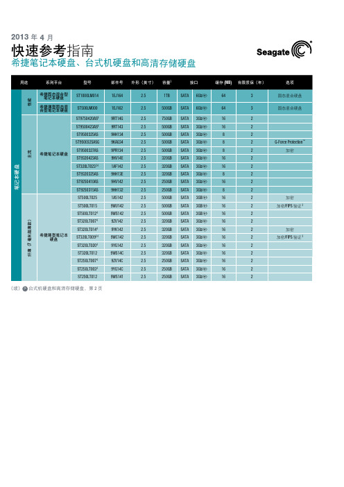
希捷笔记本硬盘、台式机硬盘和高清存储硬盘希捷合作伙伴项目成员请访问“销售工具”部分以获取最新产品路线图、生命周期终止计划和产品信息。
分销商欧洲、中东和非洲地区希捷合作伙伴项目支持00-800-6890-8282美国销售支持1-800-SEAGATE 或 1-405-324-4700请访问 以获得更多信息或致电 1-800-SEAGATE (1-800-732-4283) © 2013 年希捷科技有限公司版权所有。
保留所有权利。
在美国印刷。
Seagate 、Seagate Technology 和 Wave 标识是希捷科技有限公司在美国和/或其他国家或地区所拥有的商标或注册商标。
Barracuda 、G-Force Protection 、Momentus 、Pipeline HD 、SmartAlign 和 SV35 Series 是希捷科技有限公司或其关联公司在美国和/或其他国家或地区所拥有的商标或注册商标。
FIPS 标识是 NIST 的认证标记,但并不暗示产品经 NIST 、美国或加拿大政府的认可。
所有其他商标或注册商标均是其各自所有者的财产。
在用于衡量硬盘容量时,一千兆字节(或 GB )等于十亿字节,一兆兆字节(或 TB )等于一万亿字节。
您的计算机操作系统可能使用不同的衡量标准,因此会报告较低的容量。
此外,一些列出的容量用于格式化和其他功能,因此无法用于数据存储。
实际传输速率可能受操作环境和其他因素影响。
包含加密技术的硬件或软件的出口或复出口会受到美国商务部工业安全局的管控(要了解更多信息,请访问 )。
希捷保留更改产品类别或规格的权利,届时不再另行通知。
QR502.15-1304CN ,2013 年 4 月希捷笔记本硬盘、台式机硬盘和高清存储硬盘全新希捷型号数字含义台式机硬盘、笔记本硬盘和高清存储硬盘ST 500 DX 001品牌容量用途属性2 个字母ST = 希捷 MX = 迈拓2 到 4 位数80 = 80GB 500 = 500GB 1500 = 1500GB 容量 > 9999GB : 10 = 10TB 15 = 15TB2 个字母DX = 高端台式机 DM = 主流 DL = 入门级LX = 高端笔记本电脑 LM = 主流笔记本电脑 LT = 薄型笔记本电脑 VX = 监控级 VM = DVR VT = 超薄 DVR3 个数字,非智能反映的属性包括:超薄款外形转速缓存接口SED, FIPS 坠落感应器接口速度如需了解型号格式的变更方式,请参阅列于以下网址的简短培训演示:/seagate/ModelNumber2可在以下网址查看 FIPS 140-2 2 级证书:/groups/STM/cmvp/documents/140-1/1401vend.htm 。
MPM MDM 变送控制器 系列产品说明书

V2.0 MPM/MDM变送控制器系列产品说明书目录1产品概述 (1)2安全警告 (1)3性能指标 (2)4外形结构 (3)5电气连接 (8)6按键设置 (9)7安装 (11)8通信指令 (12)9责任 (13)本公司保留由于产品技术和工艺更新对本说明书的修改权。
若有更改,不再另行通知。
请注意本说明书的最新版本。
本公司保留对本说明书的最终解释权。
非常感谢您选用麦克传感器股份有限公司产品。
在您使用本系列产品之前,请仔细阅读说明书。
1产品概述MPM/MDM系列变送控制器是压力、差压、液位测控的智能化仪表,由MPM/MDM484C、MPM/MDM460、MPM460W、MPM/MDM484ZL四个子系列组成。
该系列产品为全电子结构,可进行现场压力/差压/液位的测量、显示与控制,输出标准信号,同时可实现基于RS485(Modbus RTU协议)总线的网络传输与变送控制器参数远程设定与调校。
使用灵活,操作简单,调节容易。
广泛应用于水电、自来水、水处理、石油、化工、冶金等各行业之中,可实现对流体介质的压力、差压、液位的测量、显示和控制。
产品具有以下特点●高精度数模转换电路,微处理器处理数据●方便组网和数据传输,可实现远程调校和设定●主、副屏同时显示(484C只有主屏)●按键设置参数和调校,操作方便●同时具有输出标准模拟信号和RS485(Modbus RTU协议)通信接口●最多可提供八路控制(460系列),控制精确高●设置回差值,取消触点抖动现象,控制可靠2安全警告使用前应仔细阅读本说明书,按每款产品电气定义接线。
在没有标准压力源时,请勿对变送器进行调校,若需调校请由专业人员操作。
请您不要用手或尖锐的东西触压波纹膜片,以免损坏传感器。
在有大的干扰环境下,应将壳体良好接地。
3性能指标测量范围:液位:0m~1m…200mHO(仅MPM460W)2压力:-100kPa…0kPa~10kPa…100MPa差压:0kPa~50kPa…3.5MPa过载压力:压力:1.5倍满量程压力或110MPa(取最小值)差压:静压≤20MPa液位:1.5倍满量程压力供电电源:220V AC或110~370V DC或24V DC输出信号:模拟量:4mA~20mADC、0mA~10/20mADC、0/1V~5/10VDC数字量:RS485接口(Modbus RTU协议)环境温度:-10℃~60℃介质温度:-10℃~80℃存储温度:-40℃~80℃(460W投入式传感器部分-20℃~80℃)相对湿度:0%~80%振动:加速度≤3g,频率0Hz~300Hz冲击:≤10g稳定性:≤±0.3%/年最大功耗:≤3.5W(460系列5~8控制点≤5W)精度:≤±0.25%FS(典型值),≤±0.5%FS(最大值)继电器负载能力:240V/3A AC或30V/3A DC触点寿命:>100000次主显示屏:0.56英寸(460系列、484C系列)或0.8英寸(484ZL系列)副显示屏:0.36英寸(460系列、484ZL系列)显示范围:-1999~9999(高亮红)数字部分:采样速度:10次/秒控制接点数:1~5点(484C系列,484ZL系列)1~8点(460系列)安装方式:垂直安装、轴向安装(MPM484ZL、MPM484C)、投入式安装防护等级:IP65:MPM460(W)与MDM460显示壳体部分IP68:MPM460W传感器部分4外形结构4.1结构材料压力接口:不锈钢感压膜片:316L不锈钢电子壳体:不锈钢密封方式:丁腈橡胶或全焊接4.2压力接口表压型:M20×1.5外螺纹差压型:G1/4内螺纹型液位(460W):传感器部分为投入式液位传感器4.3外形图a)MPM/MDM484C型系列产品外形图图b)MPM460型、MDM460型、MPM460W型外形图MPM460型压力变送控制器外形图MDM460型差压变送控制器外形图MPM460W 型变送控制器外形图MPM460WK 型变送控制器外形图c)MPM484ZL 型压力变送控制器外形图MDM484ZL 型差压变送控制器外形图(垂直安装方式)MPM484ZL 型压力变送控制器外型图(轴向安装)注:轴向安装的变送控制器和垂直安装的变送控制器的接口尺寸是一致。
- 1、下载文档前请自行甄别文档内容的完整性,平台不提供额外的编辑、内容补充、找答案等附加服务。
- 2、"仅部分预览"的文档,不可在线预览部分如存在完整性等问题,可反馈申请退款(可完整预览的文档不适用该条件!)。
- 3、如文档侵犯您的权益,请联系客服反馈,我们会尽快为您处理(人工客服工作时间:9:00-18:30)。
How to Order - MDM-PCB SeriesMDM-PCB connectors are designed for use with flex circuitry, flat cable and printed circuit boards or multi-layer boards. They use the standard MDM metal shell and provide high density and high reliability in board-to-board,board-to-cable and cable-to-cable applications.MDM-PCB connectors are available in 8 shell sizes with 9 to 100 contacts. Terminations may be straight (BS) or at 90˚ right angle (BR,CBR) board thickness. Jackpost mounting for use with locking hardware is also available.SERIESINSULATOR MATERIALCONTACT ARRANGEMENTCONTACT TYPE TERMINATION TYPEMOUNTING HARDWARE (Shell Flange) MOUNTING HARDWARE FOR PCBTERMINATION TAIL LENGTH MODIFICATION CODE SHELL FINISH MODIFICATION CODESSERIESMOUNTING HARDWARE FOR PCB TERMINATION TAIL LENGTH MODIFICATION CODE SHELL FINISH MODIFICATION CODESINSULATOR MATERIALCONTACT ARRANGEMENTCONTACT TYPETERMINATION TYPEMOUNTING HARDWARE (Shell Flange)MDM - Micro "D" Metal Shell T -Threaded Insert#2-56 Thd for Shell Sizes 9 thru 51 #4-40 Thd for Shell Size 100No letter - noneNone - .109 (2.77) ±.015 (0.38) Standard L61 - .125 (3.18)L56 - .150 (3.81)L57 - .190 (4.83)L39 - .250 (6.35)L58 - .375 (9.52)None - Yellow Chromate/Cadmium over Nickel A174 - Electroless Nickel A172 - Gold over Nickel A141 - Irridite/Alodine A30 - Black Anodize (For special modification codes, consult customer service.)NOTE: Back molding material – Epoxy Hysol #MG40FSMDM * - - 25PP BSTL39 A174Liquid Crystal Polymer (LCP)9, 15, 21, 25, 31, 37, 51, and 100P -Pin (Plug)S -Socket (Receptacle)BS - Straight PCB Termination BR - Right Angle PCB TerminationCBR - Right Angle Narrow Profile PCB Terminations P -Jackposts M7 - Jackposts M83513/5-07 (Sizes 9-51)M17 - JackpostsM83513/5-17 (Size 100)No letter - none RoHS COMPLIANCE RBS (Board Straight) Series.120 ± .005(3.05 ± 0.13)Size 100(9-51).JACKPOST (100)#4-40 UNC-2B TYP ..186 (4.72) MAX. PLUG.109 ± 0.15(2.77 ± 0.38).050(1.27).050.050.100TYP ..150.050(1.27).050.050.150TYP .PCB Termination Arrangements* (Viewed from PCB solder side)9Contacts 31 Contacts 15 Contacts100 Contacts51 Contacts21 Contacts25 ContactsIdentification number shown for plug connector, use reverse order for socket connector.NOTE: Standard lead termination is #24 AWG, solid copper, solder or tin dipped All Termination Configurations .100 (2.54) x .100 (2.54) Grid Pattern, Offset .050 (1.27)NOTE: Dimensions shown are for reference only-consult factory for final design dimensions.REF.B±.007 (.18)Part Number By Shell Size A Max.C±.005 (.13)D Max.E Max.F Max.G Max.H Max.J Max.K Max.MDM-9PBS*MDM-9SBS*MDM-15PBS*MDM-15SBS*MDM-21PBS*MDM-21SBS*MDM-25PBS MDM-25SBS*MDM-31PBS*MDM-31SBS*MDM-37PBS*MDM-37SBS*MDM-51PBS*MDM-51SBS*MDM-100PBS*1.390 (35.31)1.390 (35.31)1.390 (35.31)1.390 (35.31)1.690 (43.93)1.690 (43.93)1.740 (44.20)1.740 (44.20)2.040 (51.82)2.040 (51.82)2.340 (59.44)2.340 (59.44)2.270 (67.66)2.270 (67.66)3.070 (77.98)1.150 (29.21)1.150 (29.21)1.150 (29.21)1.150 (29.21)1.450 (36.83)1.450 (36.83)1.500 (38.10)1.500 (38.10)1.800 (45.72)1.800 (45.72)2.100 (53.34)2.100 (53.34)2.000 (50.80)2.000 (50.80)2.800 (71.12).565 (14.35).565 (14.35).715 (18.16).715 (18.16).865 (21.97).865 (21.97).965 (24.51).965 (24.51)1.115 (28.32)1.115 (28.32)1.265 (32.13)1.265 (32.13)1.215 (30.86)1.215 (30.86)1.800 (45.72).785 (19.94).785 (19.94).935 (23.75).935 (23.75)1.085 (27.56)1.085 (27.56)1.185 (30.10)1.185 (30.10)1.335 (33.91)1.335 (33.91)1.485 (37.72)1.485 (37.72)1.435 (36.45)1.435 (36.45)2.175 (55.24).334 (8.48).402 (10.21).484 (12.29).552 (13.97).634 (16.10).702 (17.83).734 (18.64).802 (20.37).884 (22.45).952 (24.18)1.034 (26.26)1.102 (27.99).984 (24.99)1.052 (26.72)1.384 (35.15).185 (4.70).253 (6.43).185 (4.70).253 (6.43).185 (4.70).253 (6.43).185 (4.70).253 (6.43).185 (4.70).253 (6.43).185 (4.70).253 (6.43).228 (5.79).296 (7.52).271 (6.88).308 (7.82).308 (7.82).308 (7.82).308 (7.82).308 (7.82).308 (7.82).308 (7.82).308 (7.82).308 (7.82).308 (7.82).308 (7.82).308 (7.82).351 (8.92).351 (8.92).460 (11.68).165 (4.19).165 (4.19).165 (4.19).165 (4.19).165 (4.19).165 (4.19).165 (4.19).165 (4.19).165 (4.19).165 (4.19).165 (4.19).165 (4.19).165 (4.19).165 (4.19).303 (7.70).355 (9.02).355 (9.02).355 (9.02).355 (9.02).355 (9.02).355 (9.02).355 (9.02).355 (9.02).355 (9.02).355 (9.02).355 (9.02).355 (9.02).355 (9.02).355 (9.02).550 (12.70).555 (14.10).555 (14.10).555 (14.10).555 (14.10).555 (14.10).555 (14.10).555 (14.10).555 (14.10).555 (14.10).555 (14.10).555 (14.10).555 (14.10).555 (14.10).555 (14.10).686 (17.42)BR (Board Right Angle) Series.300PCB Termination Arrangements (Viewed from bottom of connector, PCB solder side.)Identification number shown for plug connector, use reverse order for socket connector..100TYP ..150.150(3.81).150(4.45).150.150.150(5.72)9Contacts31 Contacts 15Contacts 37 Contacts 51 Contacts21 Contacts25 Contacts27 28 29 30 31 32 33 3435 36 37 38 39 40 41 42 43 44 45 46 47 48 49 50 511234567891011 12 13 14 15 16 17 18 19 20 21 22 23 24 25 26100 ContactsNOTE: Standard lead termination is #24 AWG, gold plated, solid copper, solder or tin dripped.*For jackpost, add letter "P" or "M7" for sizes 9-51, "M17" for size 100.Part Number By Shell Size MDM-9PBR*MDM-9SBR*MDM-15PBR*MDM-15SBR*MDM-21PBR*MDM-21SBR*MDM-25PBR*MDM-25SBR*MDM-31PBR*MDM-31SBR*MDM-37PBR*MDM-37SBR*MDM-51PBR*MDM-51SBR*MDM-100PBR*MDM-100SBR*1.390 (35.31)1.390 (35.31)1.540 (39.12)1.540 (39.12)1.690 (42.93)1.690 (42.93)1.790 (45.47)1.790 (45.47)2.040 (51.82)2.040 (51.52)2.340 (59.44)2.340 (59.44)1.875 (47.63)1.875 (47.63) 2.74 (69.72) 2.74 (69.72)1.150 (29.21)1.150 (29.21)1.300 (33.02)1.300 (33.02)1.450 (36.83)1.450 (36.83)1.550 (39.37)1.550 (39.37)1.800 (45.72)1.800 (45.72)2.100 (53.34)2.100 (53.34)1.600 (40.64)1.600 (40.64)2.500 (63.50)2.500 (63.50).565 (14.35).565 (14.35).715 (18.16).715 (18.16).865 (21.97).865 (21.97).965 (24.51).965 (24.51)1.115 (28.32)1.115 (28.32)1.265 (32.13)1.265 (32.13)1.215 (30.86)1.215 (30.86)1.800 (45.72)1.800 (45.72).334 (8.48).402 (10.21).484 (12.29).552 (13.97).634 (16.10).702 (17.83).734 (18.64).802 (20.37).884 (22.45).952 (24.18)1.034 (26.26)1.102 (27.99).984 (24.99)1.052 (26.72)1.384 (35.15)1.508 (38.10).185 (4.70).253 (6.43).185 (4.70).253 (6.43).185 (4.70).253 (6.43).185 (4.70).253 (6.43).185 (4.70).253 (6.43).185 (4.70).253 (6.43).228 (5.79).296 (7.52).271 (6.88).394 (10.01).455 (11.56).455 (11.56).455 (11.56).455 (11.56).455 (11.56).455 (11.56).455 (11.56).455 (11.56).455 (11.56).455 (11.56).455 (11.56).455 (11.56).565 (14.35).565 (14.35).755 (19.18).755 (19.18).308 (7.82).308 (7.82).308 (7.82).308 (7.82).308 (7.82).308 (7.82).308 (7.82).308 (7.82).308 (7.82).308 (7.82).308 (7.82).308 (7.82).351 (8.92).351 (8.92).394 (10.01).394 (10.01)A Max.B±.007 (.18)C±.005 (.13)D Max.E Max.F Max.G Max.All Termination Configurations .100 (2.54) x .100 (2.54) Grid Pattern, Offset .050 (1.27).CBR (Condensed Board Right Angle) SeriesPCB Termination Arrangements (Viewed from bottom of connector, PCB solder side.)Identification number shown for plug connector, use reverse order for socket connector.135724101214161719212325272937394143454749512830323436384042444648505355575961636567697173755254565860626466687072747678808284868890929496981007779818385878991939597991820222631333524689111315JACKPOST 2-56..186 (4.72)MAX.PLUG .198 (5.03)DIA.TYP .(Size 9-51)FOR 31: 1.085(27.56) MAX.FOR 37: 1.185(30.10) MAX.FOR 51: 1.225(31.12) MAX.**JACKPOST .100 VIEW.108.020.020(2.54 ± 0.13)9Contacts View X15Contacts View X21Contacts View X25 Contacts View X100 Contacts View W51 Contacts View Y 37 Contacts View Y 31 Contacts View Y NOTE: Standard lead termination is #24 AWG, solid copper, solder or tin dripped. *For jackpost, add letter "P" or "M7" for sizes 9-51, "M17" for size 100.By Shell Size MDM-9PCBR*MDM-9SCBR*MDM-15PCBR*MDM-15SCBR*MDM-21PCBR*MDM-21SCBR*MDM-25PCBR*MDM-25SCBR*MDM-31PCBR*MDM-31SCBR*MDM-37PCBR*MDM-37SCBR*MDM-51PCBR*MDM-51SCBR*MDM-100PCBR*MDM-100SCBR*.785 (19.94) .785 (19.94) .935 (23.75) .935 (23.75) 1.085 (27.56) 1.085 (27.56) 1.185 (30.10) 1.185 (30.10) 1.335 (33.91) 1.335 (33.91) 1.485 (37.72) 1.485 (37.72) 1.435 (36.45) 1.435 (36.45) 2.170 (55.12) 2.170 (55.12).565 (14.35) .565 (14.35) .715 (18.16) .715 (18.16) .865 (21.97) .865 (21.97) .965 (24.51) .965 (24.51) 1.115 (28.32) 1.115 (28.32) 1.265 (32.13) 1.265 (32.13) 1.215 (30.86) 1.215 (30.86) 1.800 (45.72) 1.800 (45.72).334 (8.48) .402 (10.21) .484 (12.29) .552 (13.97) .634 (16.10) .702 (17.83) .734 (18.64) .802 (20.37) .884 (22.45) .952 (24.18) 1.034 (26.26) 1.102 (27.99) .984 (24.99) 1.052 (26.72) 1.384 (35.15) 1.508 (38.10).308 (7.82) .308 (7.82) .308 (7.82) .308 (7.82) .308 (7.82) .308 (7.82) .308 (7.82) .308 (7.82) .308 (7.82) .308 (7.82) .308 (7.82) .308 (7.82) .351 (8.92) .351 (8.92) .394 (10.01) .394 (10.01).185 (4.70) .253 (6.43) .185 (4.70) .253 (6.43) .185 (4.70) .253 (6.43) .184 (4.70) .253 (6.43) .185 (4.70) .253 (6.43) .185 (4.70) .253 (6.43) .228 (5.79) .296 (7.52) .271 (6.88) .394 (10.01).420 (10.67) .420 (10.67) .420 (10.67) .420 (10.67) .420 (10.67) .420 (10.67) .420 (10.67) .420 (10.67) .520 (13.21) .520 (13.21) .520 (13.21) .520 (13.21) .650 (16.15) .650 (16.15) 1.000 (25.40) 1.000 (25.40).250 (6.35) .250 (6.35) .250 (6.35) .250 (6.35) .250 (6.35) .250 (6.35) .250 (6.35) .250 (6.35) .250 (6.35) .250 (6.35) .250 (6.35) .250 (6.35) .300 (7.62) .300 (7.62) .400 (10.16) .400 (10.16).230 (5.81) .230 (5.81) .130 (3.30) .130 (3.30) .130 (3.30) .130 (3.30) .130 (3.30) .130 (3.30) .130 (3.30) .130 (3.30) .130 (3.30) .130 (3.30) .150 (3.81) .150 (3.81) .200 (5.08) .200 (5.08)Max.±.005 (.13)±.010 (.25)±.010 (.25)Max.Max.Max.Max.All Termination Configurations .100 (2.54) x .100 (2.54) Grid Pattern, Offset .050 (1.27).。