G923-200T1U中文资料
美国MOTOROLA 压力传感器说明书

美国MOTOROLA压力传感器美国MOTOROLA公司的MPX系列硅压力传感器,主要以气压测量为主,适合用于医疗器械,气体压力控制等领域,输出数字信号。
其测量方式可分为:表压(GP)、绝压(A、AP)、差压(D、DP)型。
在宽温度范围工作时需外加补偿网络和信号调整电路。
具体型号分类而定名称:MPX2010DP 名称:MPX5700DP MPX5700GP 名称:MPX2100AP名称:MPX5500DP 名称:MPX5100AP 名称:MPX5050DP名称:MPX5010DP 名称:MPX4115AP 名称:MPX2200A 名称:MPX2200AP 名称:MPXH6115A6U 名称:MPX4250DP名称:MPX4115A 名称:MPX2202DP 名称:MPX2102AP名称:MPX2053GP 名称:MPXY8300A6U 压力传感器 名称:触力型压力传感器 FSG15N1A 名称:硅压力传感器 MPXH6115A 名称:MPX5700DP 硅压力传感器 名称:MPX53GP 硅压力传感器 名称:压力传感器FPM07 名称:轮胎压力传感器TP015 名称:轮胎压力传感器NPP301名称:Freescale 压力传感器 MPX2010DP商斯达实业传感器与智能控制分公司专门从事各种进口传感器的营销工作,代理多家欧美知名公司的产品。
涉及压力、温度、湿度、电流、液位、磁阻、霍尔、流量、称重、光纤、倾角、扭矩、气体、光电、位移、触力、红外、速度、加速度等多种产品。
广泛应用于航空航天、医疗器械(如血压计)、工业控制、冶金化工、汽车制造、教育科研等领域。
商斯达实业代理的品牌产品主要有:压 力:Kulite、ACSI、Honeywell、Entran、Gems、Dwyer、SSI、Smi、Senstronics、Intersema、Motorola、 NAIS、E+H、Fujikura、Dytran、APM称重测力:Transcell、HBM、Interface、Thamesside、Philips、Entran 温 湿 度:Honeywell、Dwyer流 量:Gems、Dwyer、Honeywell、Folwline、WorldMagnetics 液 位:Honeywell、Siccom、Gems、Dwyer、Kulite、SSI 加 速 度:Entran、Silicondesigns、Dytran 压力开关:ACSI、Gems、Dwyer、台湾矽微航空器材:TexTech 隔音材料、Honeywell 薄膜加热片、DigirayX 射线探伤仪 仪 表:Honeywell、Transcell、东辉、上润、AD、东崎商斯达实业 除代理上述产品外,还有几条传感器生产线,一条压力传感器组装线,可为用户提供各种用途的、特殊要求的配套产品。
编辑校对资料——化学符号正斜体标准(精校版)
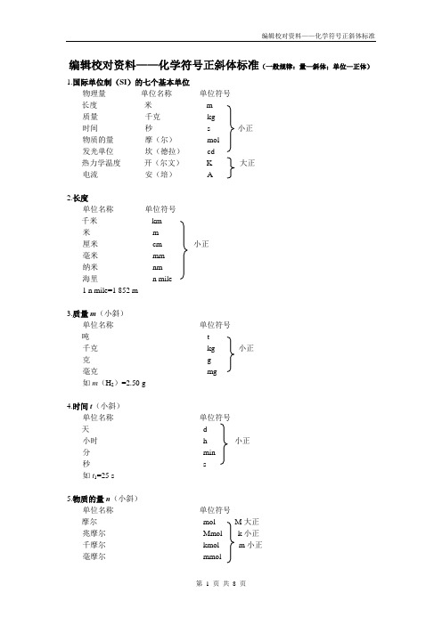
编辑校对资料——化学符号正斜体标准(一般规律:量—斜体;单位—正体)1.国际单位制(SI)的七个基本单位物理量单位名称单位符号长度米m质量千克kg时间秒s 小正物质的量摩(尔)mol发光单位坎(德拉)cd热力学温度开(尔文)K 大正电流安(培) A2.长度单位名称单位符号千米km米m厘米cm 小正毫米mm纳米nm海里n mile1 n mile=1 852 m3.质量m(小斜)单位名称单位符号吨t千克kg 小正克g毫克mg如m(H2)=2.50 g4.时间t(小斜)单位名称单位符号天 d小时h 小正分min秒s如t1=25 s5.物质的量n(小斜)单位名称单位符号摩尔mol M大正兆摩尔Mmol k小正千摩尔kmol m小正毫摩尔mmol使用该物理量时,包括使用其导出量时必须指明基本单元。
基本单元可以是原子、分子、离子、电子以及其他粒子或这些粒子的特定组合。
例如:n(H2SO4)=1 mol。
《物质的量》常用符号:摩尔质量M(大斜)阿伏加德罗常数N A(N大斜,A大正,下标)(近似值6.02×10²³ mol1-)气体摩尔体积V m(V大斜,m小正,下标)(0.224 141 0 m3·mol1-)相对分子质量M r(M大斜,r小正,下标)相对原子质量A r(A大斜,r小正,下标)粒子数N(大斜)6.体积V(大斜)单位名称单位符号立方米m3(小正)升L(大正)立方厘米cm3(小正)毫升mL(m小正)如V(O2)=22.4 L V〔NaOH(aq)〕=12.20 mL7.物质的量浓度c(小斜)单位mol/L或mol·L1-(mol小正,L大正)如c(OH-)=0.01 mol/L c(H2SO4)=0.25 mol·L1-8.温度热力学温度T(大斜)单位K(大正)如T1=215 K摄氏温度t(小斜)单位℃(大正)如t2=25 ℃标准状况温度273.15 K或0 ℃超导临界温度T C。
G2309中文资料
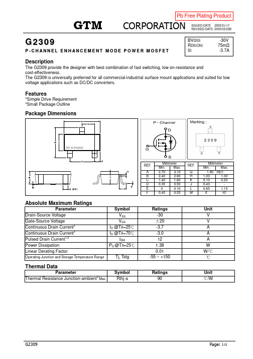
ISSUED DATE :2005/01/17 REVISED DATE :2005/03/22BG 2309P -C H A N N E L E N H A N C E M E N T M O D E P O W E R M O S F E TDescriptionThe G2309 provide the designer with best combination of fast switching, low on-resistance and cost-effectiveness.The G2309 is universally preferred for all commercial-industrial surface mount applications and suited for low voltage applications such as DC/DC converters.Features*Simple Drive Requirement *Small Package OutlineMillimeter Millimeter REF . Min. Max. REF . Min. Max. A 2.70 3.10 G1.90 REF . B2.40 2.80 H 1.00 1.30 C 1.40 1.60 K 0.10 0.20 D 0.35 0.50 J 0.40 - E 0 0.10 L 0.85 1.15 F0.45 0.55M0 10Unit V V A A A W W/ Thermal Data ParameterSymbol Ratings Unit Thermal Resistance Junction-ambient 3Max.Rthj-a90/WBV DSS -30V R DS(ON) 75m I D -3.7APb Free Plating ProductElectrical Characteristics(Tj = 25 Unless otherwise specified)ParameterSymbol Min. Typ. Max. Unit Test Conditions Drain-Source Breakdown VoltageBV DSS-30 - - VV GS =0, I D =-250uABreakdown Voltage Temperature CoefficientBV DSS /Tj- -0.02 - V/ Reference to 25 , I D =-1mA Gate Threshold Voltage V GS(th) -1.0 - -3.0 V V DS =V GS , I D =-250uA Forward Transconductance g fs - 5.0 - S V DS =-10V, I D =-3A Gate-Source Leakage CurrentI GSS - - 100 nA V GS = 20V Drain-Source Leakage Current(Tj=25 ) - - -1 uA V DS =-30V, V GS =0 Drain-Source Leakage Current(Tj=55 )I DSS- - -25 uA V DS =-24V, V GS =0 - - 75 V GS =-10V, I D =-3A Static Drain-Source On-Resistance R DS(ON) - - 120 mV GS =-4.5V, I D =-2.6A Total Gate Charge 2 Q g - 5 8 Gate-Source Charge Q gs - 1 - Gate-Drain (“Miller”) Change Q gd - 3 - nCI D =-3A V DS =-24V V GS =-4.5V Turn-on Delay Time 2 T d(on) - 8 - Rise TimeT r - 5 - Turn-off Delay Time T d(off) - 20 - Fall Time T f - 7 - nsV DS =-15V I D =-1A V GS =-10V R G =3.3 R D =15 Input Capacitance C iss - 412 660 Output CapacitanceC oss - 91 - Reverse Transfer CapacitanceC rss-62-pFV GS =0V V DS =-25V f=1.0MHzSource-Drain DiodeParameterSymbol Min. Typ. Max. Unit Test Conditions Forward On Voltage 2 V SD - - -1.2 V I S =-1.2A, V GS =0VReverse Recovery Time 2T rr - 20 - nsReverse Recovery ChargeQ rr-15-nC I S =-3A, V GS =0V dI/dt=100A/ sNotes: 1. Pulse width limited by Max. junction temperature. 2. Pulse width 300us, duty cycle 2% .3. Surface mounted on 1 in 2 copper pad of FR4 board;270 /W when mounted on min. copper pad.Characteristics CurveFig 1. Typical Output Characteristics Fig 2. Typical Output CharacteristicsFig 3. On-Resistance v.s. Gate VoltageFig 4. Normalized On-Resistancev.s. Junction TemperatureFig 6. Gate Threshold Voltage v.s.Junction TemperatureFig 5. Forward Characteristics of Reverse DiodeFig 9. Maximum Safe Operating Area Fig 10. Effective Transient Thermal ImpedanceFig 7. Gate Charge Characteristics Fig 8. Typical Capacitance CharacteristicsFig 11. Switching Time WaveformFig 12. Gate Charge Waveform。
G5131-25T11U中文资料
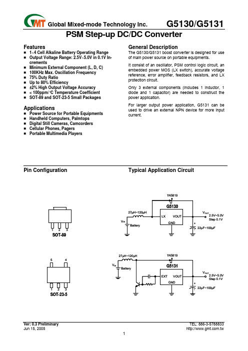
PSM Step-up DC/DC ConverterFeatures1~4 Cell Alkaline Battery Operating Range Output Voltage Range: 2.5V~5.0V in 0.1V In-crementsMinimum External Component (L, D, C)100KHz Max. Oscillation Frequency75% Duty RatioUp to 80% Efficiency±2% High Output Voltage Accuracy< 100ppm/°C Temperature CoefficientSOT-89 and SOT-23-5 Small Packages ApplicationsPower Source for Portable EquipmentsHandheld Computers, PalmtopsDigital Still Cameras, CamcordersCellular Phones, PagersPortable Multimedia Players General DescriptionThe G5130/G5131 boost converter is designed for use of main power source on portable equipments.It consist of an oscillator, PSM control logic circuit, an embedded power MOS (LX switch), accurate voltage reference, error amplifier, feedback resistors, and LX protection circuit.Only 3 external components (includes 1 inductor, 1 diode and 1 capacitor) are needed to construct the power application.For larger output power application, G5131 can be used to drive an external NPN device for more input current.Pin Configuration Typical Application Circuit2.5V~5.0V2.5V~5.0VStep 0.1VStep 0.1VOrdering InformationORDER NUMBER ORDER NUMBER(Pb free)MARKINGOUTPUTVOLTAGE (V)TEMP.RANGEPACKAGEG5130-30T11U G5130-30T11Uf EA30x 3.0 -40°C ~ +85°C SOT-23-5G5130-33T11U G5130-33T11Uf EA33x 3.3 -40°C ~ +85°C SOT-23-5G5130-42T11U G5130-42T11Uf EA42x 4.2 -40°C ~ +85°C SOT-23-5G5130-50T11U G5130-50T11Uf EA50x 5.0 -40°C ~ +85°C SOT-23-5G5130-30T21U G5130-30T21Uf 5130Fx 3.0 -40°C ~ +85°C SOT-89G5130-33T21U G5130-33T21Uf 5130Ix 3.3 -40°C ~ +85°C SOT-89G5130-42T21U G5130-42T21Uf 5130Rx 4.2 -40°C ~ +85°C SOT-89G5130-50T21U G5130-50T21Uf 5130Zx 5.0 -40°C ~ +85°C SOT-89G5131-30T11U G5131-30T11Uf EB30x 3.0 -40°C ~ +85°C SOT-23-5G5131-33T11U G5131-33T11Uf EB33x 3.3 -40°C ~ +85°C SOT-23-5G5131-42T11U G5131-42T11Uf EB42x 4.2 -40°C ~ +85°C SOT-23-5G5131-50T11U G5131-50T11Uf EB50x 5.0 -40°C ~ +85°C SOT-23-5G5131-30T21U G5131-30T21Uf 5131Fx 3.0 -40°C ~ +85°C SOT-89G5131-33T21U G5131-33T21Uf 5131Ix 3.3 -40°C ~ +85°C SOT-89G5131-42T21U G5131-42T21Uf 5131Rx 4.2 -40°C ~ +85°C SOT-89G5131-50T21U G5131-50T21Uf 5131Zx 5.0 -40°C ~ +85°C SOT-89For other output voltage, please contact us at sales@Order Number IdentificationGXXXX XX XXTypePin OptionTypeVoltage OptionPart NumberG5130: Internal MOS (LX)G5131: External MOS (EXT)PACKAGE TYPE PIN OPTION PACKINGT1 : SOT-23-5 SOT89 SOT23-5U & D: Tape & Reel Direction T2 : SOT-89 1 2 3 1 2 3 4 5G5130 1:GND VOUT LX 1:CE VOUT NC GND LXG5131 1:GND VOUT EXT 1:CE VOUT NC GND EXTORDER NUMBER ORDER NUMBER(Pb free)OUTPUTVOLTAGE (V)MARKINGG5130-25T11U G5130-25T11Uf 2.5 EA25x G5130-26T11U G5130-26T11Uf 2.6 EA26x G5130-27T11U G5130-27T11Uf 2.7 EA27x G5130-28T11U G5130-28T11Uf 2.8 EA28x G5130-29T11U G5130-29T11Uf 2.9 EA29x G5130-30T11U G5130-30T11Uf 3.0 EA30x G5130-31T11U G5130-31T11Uf 3.1 EA31x G5130-32T11U G5130-32T11Uf 3.2 EA32x G5130-33T11U G5130-33T11Uf 3.3 EA33x G5130-34T11U G5130-34T11Uf 3.4 EA34x G5130-35T11U G5130-35T11Uf 3.5 EA35x G5130-36T11U G5130-36T11Uf 3.6 EA36x G5130-37T11U G5130-37T11Uf 3.7 EA37x G5130-38T11U G5130-38T11Uf 3.8 EA38x G5130-39T11U G5130-39T11Uf 3.9 EA39x G5130-40T11U G5130-40T11Uf 4.0 EA40x G5130-41T11U G5130-41T11Uf 4.1 EA41x G5130-42T11U G5130-42T11Uf 4.2 EA42x G5130-43T11U G5130-43T11Uf 4.3 EA43x G5130-44T11U G5130-44T11Uf 4.4 EA44x G5130-45T11U G5130-45T11Uf 4.5 EA45x G5130-46T11U G5130-46T11Uf 4.6 EA46x G5130-47T11U G5130-47T11Uf 4.7 EA47x G5130-48T11U G5130-48T11Uf 4.8 EA48x G5130-49T11U G5130-49T11Uf 4.9 EA49x G5130-50T11U G5130-50T11Uf 5.0 EA50x Note: T1: SOT-23-5Selector GuideORDER NUMBER ORDER NUMBER(Pb free)OUTPUTVOLTAGE (V)MARKINGG5130-25T21U G5130-25T21Uf 2.5 5130Ax G5130-26T21U G5130-26T21Uf 2.6 5130Bx G5130-27T21U G5130-27T21Uf 2.7 5130Cx G5130-28T21U G5130-28T21Uf 2.8 5130Dx G5130-29T21U G5130-29T21Uf 2.9 5130Ex G5130-30T21U G5130-30T21Uf 3.0 5130Fx G5130-31T21U G5130-31T21Uf 3.1 5130Gx G5130-32T21U G5130-32T21Uf 3.2 5130Hx G5130-33T21U G5130-33T21Uf 3.3 5130Ix G5130-34T21U G5130-34T21Uf 3.4 5130Jx G5130-35T21U G5130-35T21Uf 3.5 5130Kx G5130-36T21U G5130-36T21Uf 3.6 5130Lx G5130-37T21U G5130-37T21Uf 3.7 5130Mx G5130-38T21U G5130-38T21Uf 3.8 5130Nx G5130-39T21U G5130-39T21Uf 3.9 5130Ox G5130-40T21U G5130-40T21Uf 4.0 5130Px G5130-41T21U G5130-41T21Uf 4.1 5130Qx G5130-42T21U G5130-42T21Uf 4.2 5130Rx G5130-43T21U G5130-43T21Uf 4.3 5130Sx G5130-44T21U G5130-44T21Uf 4.4 5130Tx G5130-45T21U G5130-45T21Uf 4.5 5130Ux G5130-46T21U G5130-46T21Uf 4.6 5130Vx G5130-47T21U G5130-47T21Uf 4.7 5130Wx G5130-48T21U G5130-48T21Uf 4.8 5130Xx G5130-49T21U G5130-49T21Uf 4.9 5130Yx G5130-50T21U G5130-50T21Uf 5.0 5130Zx Note: T2: SOT-89ORDER NUMBER ORDER NUMBER(Pb free)OUTPUTVOLTAGE (V)MARKINGG5131-25T11U G5131-25T11Uf 2.5 EB25x G5131-26T11U G5131-26T11Uf 2.6 EB26x G5131-27T11U G5131-27T11Uf 2.7 EB27x G5131-28T11U G5131-28T11Uf 2.8 EB28x G5131-29T11U G5131-29T11Uf 2.9 EB29x G5131-30T11U G5131-30T11Uf 3.0 EB30x G5131-31T11U G5131-31T11Uf 3.1 EB31x G5131-32T11U G5131-32T11Uf 3.2 EB32x G5131-33T11U G5131-33T11Uf 3.3 EB33x G5131-34T11U G5131-34T11Uf 3.4 EB34x G5131-35T11U G5131-35T11Uf 3.5 EB35x G5131-36T11U G5131-36T11Uf 3.6 EB36x G5131-37T11U G5131-37T11Uf 3.7 EB37x G5131-38T11U G5131-38T11Uf 3.8 EB38x G5131-39T11U G5131-39T11Uf 3.9 EB39x G5131-40T11U G5131-40T11Uf 4.0 EB40x G5131-41T11U G5131-41T11Uf 4.1 EB41x G5131-42T11U G5131-42T11Uf 4.2 EB42x G5131-43T11U G5131-43T11Uf 4.3 EB43x G5131-44T11U G5131-44T11Uf 4.4 EB44x G5131-45T11U G5131-45T11Uf 4.5 EB45x G5131-46T11U G5131-46T11Uf 4.6 EB46x G5131-47T11U G5131-47T11Uf 4.7 EB47x G5131-48T11U G5131-48T11Uf 4.8 EB48x G5131-49T11U G5131-49T11Uf 4.9 EB49x G5131-50T11U G5131-50T11Uf 5.0 EB50x Note: T1: SOT-23-5Selector GuideORDER NUMBER ORDER NUMBER(Pb free)OUTPUTVOLTAGE (V)MARKINGG5131-25T21U G5131-25T21Uf 2.5 5131Ax G5131-26T21U G5131-26T21Uf 2.6 5131Bx G5131-27T21U G5131-27T21Uf 2.7 5131Cx G5131-28T21U G5131-28T21Uf 2.8 5131Dx G5131-29T21U G5131-29T21Uf 2.9 5131Ex G5131-30T21U G5131-30T21Uf 3.0 5131Fx G5131-31T21U G5131-31T21Uf 3.1 5131Gx G5131-32T21U G5131-32T21Uf 3.2 5131Hx G5131-33T21U G5131-33T21Uf 3.3 5131Ix G5131-34T21U G5131-34T21Uf 3.4 5131Jx G5131-35T21U G5131-35T21Uf 3.5 5131Kx G5131-36T21U G5131-36T21Uf 3.6 5131Lx G5131-37T21U G5131-37T21Uf 3.7 5131Mx G5131-38T21U G5131-38T21Uf 3.8 5131Nx G5131-39T21U G5131-39T21Uf 3.9 5131Ox G5131-40T21U G5131-40T21Uf 4.0 5131Px G5131-41T21U G5131-41T21Uf 4.1 5131Qx G5131-42T21U G5131-42T21Uf 4.2 5131Rx G5131-43T21U G5131-43T21Uf 4.3 5131Sx G5131-44T21U G5131-44T21Uf 4.4 5131Tx G5131-45T21U G5131-45T21Uf 4.5 5131Ux G5131-46T21U G5131-46T21Uf 4.6 5131Vx G5131-47T21U G5131-47T21Uf 4.7 5131Wx G5131-48T21U G5131-48T21Uf 4.8 5131Xx G5131-49T21U G5131-49T21Uf 4.9 5131Yx G5131-50T21U G5131-50T21Uf 5.0 5131Zx Note: T2: SOT-89Absolute Maximum RatingsLX to GND…………….…..……………..…-0.3V to +7V CE to GND….……………..………..……...-0.3V to +7V VOUT to GND.…….…..................……….-0.3V to +7V Operating Temperature Range (Note 1)..-40°C to +85°CJunction Temperature ......…......…......……........+125°C Storage Temperature…………........…..-65°C to +150°C Reflow Temperature (soldering, 10 sec)…..…....+260°CStress beyond those listed under “Absolute Maximum Rating” may cause permanent damage to the device.Electrical Characteristics(V OUT = 3.3V, V IN = 1.8V, T A = 25°C )PARAMETER CONDITION MIN TYP MAX UNITOutput Voltage Accuracy-2 --- +2 % Input Voltage Range ------6.5VStart-up Voltage --- 0.9 ---VHold-on Voltage--- 0.5 --- VNo Switching (I DD2) --- 10 15 µASwitching (I DD1) --- 20 --- µAInput CurrentNo Load (I IN ) ---30 --- µA LX Switch On ResistanceV LX = 0.4V --- 2 6Ω LX Leakage Current V LX = 6.0V --- --- 0.1 µAMaximum Oscillation Frequency 70 100 130 KHzDuty Cycle65 75 85 %V LX Voltage Limit--- 1 --- V Efficiency--- 80 --- %Note 1: The G5130 are guaranteed to meet performance specifications from 0°C to 85°C. Specifications over the -40°C to 85°Coperating temperature range are assured by design, characterization and correlation with statistical process controls.Block DiagramCELX VOUTTypical Performance Characteristics(V IN= +3.0V, L=100µH, T A=25°C, unless otherwise noted.)Line Transient Load TransientRecommended Minimum FootprintSOT-89SOT-23-5Power On ResponsePackage InformationSOT-23-5 (T1) PackageNote:1. Package body sizes exclude mold flash protrusions or gate burrs2. Tolerance ±0.1000 mm (4mil) unless otherwise specified3. Coplanarity: 0.1000mm4. Dimension L is measured in gage planeDIMENSIONS IN MILLIMETERSYMBOLMIN NOM MAXA 1.00 1.10 1.30A1 0.00 ----- 0.10A2 0.70 0.80 0.90 b 0.35 0.40 0.50C 0.10 0.15 0.25D 2.70 2.90 3.10E 1.40 1.60 1.80e ----- 1.90(TYP) ----- e1 ----- 0.95 ----- H 2.60 2.80 3.00L 0.37 ------ ----- θ1 1º 5º9ºSOT-89 (T2) PackageDIMENSIONS IN MILLIMETER DIMENSIONS IN INCH SYMBOLMIN NOM MAX MIN NOM MAXA 1.40 1.50 1.60 0.055 0.059 0.063 A1 0.80 1.04 ----- 0.031 0.041 ----- b 0.36 0.42 0.48 0.014 0.016 0.018 b1 0.41 0.47 0.53 0.016 0.018 0.020 C 038 0.40 0.43 0.014 0.015 0.017 D 4.404.50 4.600.173 0.177 0.181 D1 1.40 1.60 1.75 0.055 0.062 0.069 HE ----- ----- 4.25 ----- ----- 0.167 E 2.40 2.50 2.60 0.094 0.098 0.102 e 2.90 3.00 3.10 0.114 0.118 0.122Taping SpecificationPACKAGE Q’TY/REELSOT-23-5 3,000 ea SOT-89 1,000 eaGMT Inc. does not assume any responsibility for use of any circuitry described, no circuit patent licenses are implied and GMT Inc. reserves the right at any time without notice to change said circuitry and specifications.SOT-89 Package OrientationSOT-23-5 Package Orientation。
JANTXV1N6642U中文资料
6 LAKE STREET, LAWRENCE, MASSACHUSETTS 01841 PHONE (978) 620-2600 FAX (781) 689-0803 WEBSITE:
157
元器件交易网
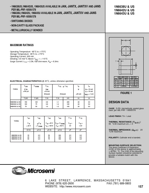
IN6638U&US, IN6642U&US
1000
100
150ºC
IR - Reverse Current - (µA)
10
100º
1
C
0.1
25ºC
.01
-65ºC
-65ºC
1
25º
C
NOTE :
All temperatures shown on graphs are junction temperatures
.001 20 40 60 80 100 120 140 Percent of Reverse Working Voltage (%) FIGURE 3 Typical Reverse Current vs Reverse Voltage
1N6638U & US 1N6642U & US 1N6643U & US
MAXIMUM RATINGS
Operating Temperature: -65°C to +175°C Storage Temperature: -65°C to +175°C Operating Current: 300 mA Derating: 4.6 mA/°C Above TEC = + 110°C Surge Current: IFSM = 2.5A, half sine wave, Pw = 8.3ms
DIM D F G S
NI 9238 4通道模拟输入模块说明书
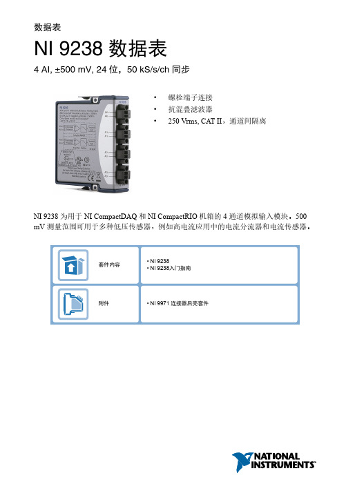
数据表NI 9238数据表4 AI, ±500 mV, 24位,50 kS/s/ch同步•螺栓端子连接•抗混叠滤波器•250 Vrms, CAT II,通道间隔离NI 9238为用于NI CompactDAQ和NI CompactRIO机箱的4通道模拟输入模块。
500 mV测量范围可用于多种低压传感器,例如高电流应用中的电流分流器和电流传感器。
NI C 系列概述NI 提供超过100种C 系列模块,用于测量、控制以及通信应用程序。
C 系列模块可连接任意传感器或总线,并允许进行高精度测量,以满足高级数据采集及控制应用程序的需求。
•与测量相关的信号调理,可连接一组传感器和信号•隔离选项包括组间、通道间以及通道对地•温度范围为-40 °C ~70 °C ,满足各种应用程序和环境需要•热插拔CompactRIO 和CompactDAQ 平台同时支持大部分C 系列模块,用户无需修改就可将模块在两个平台间转换。
CompactRIOCompactRIO 将开放嵌入式架构与小巧、坚固以及C 系列模块进行了完美融合,是一种由NI LabVIEW 驱动的可重配置I/O (RIO )架构。
每个系统包含一个FPGA ,用于自定义定时、触发以及处理一系列可用的模块化I/O ,可满足任何嵌入式应用程序的需求。
2 | | NI 9238数据表CompactDAQCompactDAQ是一种便携、耐用的数据采集平台,其模块化I/O集成了连接、数据采集以及信号调理功能,可直接接入任意传感器或信号。
配合LabVIEW使用CompactDAQ,用户可轻松地定义如何采集、分析、可视化以及管理测量数据。
软件LabVIEW专业版开发系统- 用于Windows•使用高级软件工具进行大型项目开发•通过DAQ助手和仪器I/O助手自动生成代码•使用高级测量分析和数字信号处理•利用DLL、ActiveX和.NET对象的开放式连接•生成DLL、可执行程序以及MSI安装程序NI LabVIEW FPGA模块•设计用于NI RIO硬件的FPGA应用程序•使用和台式及实时应用程序一样的图形化环境进行编程•以最高为300 MHz的循环速率执行控制算法•实现自定义定时和触发逻辑、数字协议以及DSP算法•集成现有HDL代码和第三方IP(包括Xilinx IP生成器函数)•作为LabVIEW Embedded Control and Monitoring Suite的一部分购买NI LabVIEW Real-Time模块•使用LabVIEW图形化编程设计确定性实时应用程序•下载至专有NI或第三方硬件,获得可靠的执行及多种I/O选择•利用内置的PID控制、信号处理以及分析函数•自动利用多核CPU或手动设置处理器关联•利用实时操作系统、开发和调试支持以及板卡支持•独立购买,或作为LabVIEW套件的一部分购买NI 9238数据表 |© National Instruments|3NI 9238 电路•每个通道的输入信号经缓冲、调理后,由模数转换器(ADC)对其采样。
安川G3中文说明书
22
AC
模拟共通
脉 冲
――
RP
输
出
――
MP
通 信
――
R+
电
――
R-
路 端
――
S+
子
――
S-
――
IG
―― ――
――
多功能脉冲输入 (出厂时:频率指令输入) 多功能脉冲监视(出厂时:输出频率) 内存总线通信输入
内存总线通信输出 通信用屏蔽线
● 端子排列/形状
G3
11 12 13 14 15 16 17 25 26 27 1 2 3 4 5 6 7 8 21 22
150Hz 时
恒定转矩用途时需要低噪音型
不要(递减转矩用途等)
没有问题可以使用。
必要
请使用 1 个等级以上的变频器。详细情况请进行
咨询。
确定变频器额定电流 >电机额定电流。
和 G3 相比 F7 额定电流小。
通常虽然没有问题,但是和 6 电极以上电机、额定电压低的电机进行配套时需要特别注意。
正转、逆转以外的 6 点全部被使用着。
G3
无端子 (不可进行 12 相整流)
―
F7
无端子 (不可进行 12 相整流)
带端子 (可以 12 相整流)
G3
无端子 (不可进行 12 相整流)
― 无端子 ―
F7
无端子 (不可进行 12 相整流)
带端子 (可以 12 相整流)
G3
带端子 (可以连接电阻器)
无端子 (无法连接电阻器)
―
F7 带端子 (可以连接电阻器)
主电路(200V 级)
容量
端子标记
G3
CSC1008中文资料

Continental Device India LimitedAn IS/ISO 9002 and IECQ Certified ManufacturerNPN/PNP EPITAXIAL PLANAR SILICON TRANSISTORSCSC1008 NPN CSA708 PNP TO-92CBELow Frequency Amplifier.ABSOLUTE MAXIMUM RATINGS(Ta=25deg C unless otherwise specified)DESCRIPTIONSYMBOL VALUE UNIT Collector -Base Voltage VCBO 80V Collector -Emitter Voltage VCEO 60V Emitter -Base Voltage VEBO 8.0V Collector CurrentIC 700mA Collector DissipationPC 800mW Operating And Storage Junction Tj, Tstg-55 to +150deg CTemperature RangeELECTRICAL CHARACTERISTICS (Ta=25 deg C Unless Otherwise Specified)DESCRIPTION SYMBOL TEST CONDITION CSC1008CSA708UNIT Collector -Base VoltageVCBO IC=100uA.IE=0>80>80V Collector -Emitter VoltageVCEO IC=10mA,IB=0>60>60V Emitter-Base VoltageVEBO IE=100uA, IC=0>8.0>8.0V Collector-Cut off CurrentICBO VCB=60V, IE=0<100<100nA Emitter-Cut off CurrentIEBO VEB=5V, IC=0<100<100nA DC Current GainhFE*IC=50mA,VCE=2V 40-40040-240Collector Emitter Saturation Voltage VCE(Sat)*IC=500mA,IB=50mA<0.4<0.7V Base Emitter Saturation Voltage VBE(Sat) *IC=500mA,IB=50mA <1.1<1.1VDYNAMIC CHARACTERISTICSTransition Frequency ft IC=50mA, VCE=10V >30typ50MHz Out-Put CapacitanceCobVCB=10V, IE=0typ8typ13pFf=1MHz*hFE CLASSIFICATION CSC1008R : 40 - 80O : 70 -140 Y : 120-240 G : 200-400CSA708R : 40 - 80O : 70 -140 Y : 120-240*Pulse Test: PW=350us, Duty Cycle=2%IS/ISO 9002Lic# QSC/L- 000019.2IS / IECQC 700000IS / IECQC 750100TO-92 Transistors on Tape and Ammo PackTO-92 Plastic PackageTO-92 Bulk TO-92 T&A1K/polybag 2K/ammo box200 gm/1K pcs 645 gm/2K pcs3" x 7.5" x 7.5"12.5" x 8" x 1.8"5.0K 2.0K17" x 15" x 13.5"17" x 15" x 13.5"80.0K 32.0K23 kgs 12.5 kgsPACKAGENet Weight/Qty DetailsSTANDARD PACKINNER CARTON BOXQty OUTER CARTON BOXQty Gr Wt SizeSizePacking Detail1. M AX IM UM A LIGNM ENT D EV IAT ION BE TW E EN LEAD S NO T TO BE G R EATER TH AN 0.2 m m.2. M AX IM UM NO N-C U M ULATIVE VAR IATIO N B ETW E EN TA PE FEE D H OLE S S HA LL NO T E XC EED 1 m m IN 20 PIT CH ES.3. H OLD DO W N TAP E NOT TO E XC EED BE YO ND TH E E DG E(S) O F C AR RIE R TAP E AND THE RE SH ALL BE NO EX PO SU R E O F AD HE SIV E.4. NO M O R E TH AN 3 CO NSE CU TIVE M ISS ING CO M P ONENTS ARE PE RM ITT ED.5. A TAP E TR AILE R, H AVING AT LE AS T TH RE E FE ED HO LES AR E R EQ UIR ED AF TER THE LAS T CO M PO NENT.6. SP LICE S S HA LL NO T INTER FER E W ITH T HE SPR O CK ET F EED H OLE S.A l l d i m i n s i o n s i n m m .DIM MIN.MAX.A4.325.33B 4.455.20C 3.18 4.19D 0.410.55E 0.350.50F 5 DEG G 1.14 1.40H 1.14 1.53K12.70—PIN CONFIGURATION 1. COLLECTOR 2. BASE 3. EMITTERNotesDisclaimerThe product information and the selection guides facilitate selection of the CDIL's Discrete Semiconductor Device(s)best suited for application in your product(s)as per your requirement.It is recommended that you completely review our Data Sheet(s)so as to confirm that the Device(s)meet functionality parameters for your application.The information furnished on the CDIL Web Site/CD is believed to be accurate and reliable.CDIL however,does not assume responsibility for inaccuracies or incomplete information.Furthermore,CDIL does not assume liability whatsoever,arising out of the application or use of any CDIL product; neither does it convey any license under its patent rights nor rights of others.These products are not designed for use in life saving/support appliances or systems.CDIL customers selling these products(either as individual Discrete Semiconductor Devices or incorporated in their end products),in any life saving/support appliances or systems or applications do so at their own risk and CDIL will not be responsible for any damages resulting from such sale(s).CDIL strives for continuous improvement and reserves the right to change the specifications of its products without prior notice.CDIL is a registered Trademark ofContinental Device India LimitedC-120 Naraina Industrial Area, New Delhi 110 028, India.Telephone + 91-11-579 6150 Fax + 91-11-579 9569, 579 5290e-mail sales@ 。
- 1、下载文档前请自行甄别文档内容的完整性,平台不提供额外的编辑、内容补充、找答案等附加服务。
- 2、"仅部分预览"的文档,不可在线预览部分如存在完整性等问题,可反馈申请退款(可完整预览的文档不适用该条件!)。
- 3、如文档侵犯您的权益,请联系客服反馈,我们会尽快为您处理(人工客服工作时间:9:00-18:30)。
300mA High PSRR LDO RegulatorsFeaturesLow, 90µA No-Load Supply Current Guaranteed 300mA Output Current Dropout Voltage is 200mV @ 150mA Load PSRR=65dB @ 120HzOver-Temperature Protection and Short-Circuit ProtectionTwo Modes of Operation ---- Fixed Mode: 1.50V~5.00VAdjustable Mode: from 1.25V to 5.50VMax. Supply Current in Shutdown Mode < 1µA Low Output Noise at 224µV RMSStable with low cost ceramic capacitorsApplicationsNotebook Computers Cellular Phones PDAsDigital still Camera and Video Recorders Hand-Held Devices Audio CodecGeneral DescriptionThe G923 is a low supply current, high PSRR, and low dropout linear regulator that comes in a space saving SOT-23-5 package. The supply current at no-load is 90µA. In the shutdown mode, the maximum supply current is less than 1µA. Operating voltage range of the G923 is from 2.50V to 5.50V. The over-current protection limit is set at 550mA typical. An over- tem-perature protection circuit is built-in in the G923 to prevent thermal overload. These power saving fea-tures make the G923 ideal for use in the bat-tery-powered applications such as notebook com-puters, cellular phones, and PDA ’s.The G923 has two modes of operation. When the SET pin is connected to ground, its output is a pre-set value: 1.50V~5.00V. There is no external component needed to decide the output voltage. When an output other than the preset value is needed, two external resistors should be used as a voltage divider. The output volt-age is then decided by the resistor ratio. The G923 comes in a space saving SOT-23-5 package.Pin ConfigurationSETOUTSOT-23-5SHDNGNDIN Adjustable modeFixed modeOrdering InformationFor other output voltage, please contact us at sales @Note: T1: SOT-23-5U: Tape & ReelSelector GuideORDER NUMBERORDER NUMBER(Pb free)OUTPUT VOLTAGE (V)MARKINGG923-150T1U G923-150T1Uf 1.50 92AAx G923-160T1U G923-160T1Uf 1.60 92ABx G923-170T1U G923-170T1Uf 1.70 92ACx G923-180T1U G923-180T1Uf 1.80 92ADx G923-190T1U G923-190T1Uf 1.90 92AEx G923-200T1U G923-200T1Uf 2.00 92AFx G923-210T1U G923-210T1Uf 2.10 92AGx G923-220T1U G923-220T1Uf 2.20 92AHx G923-230T1U G923-230T1Uf 2.30 92AIx G923-240T1U G923-240T1Uf 2.40 92AJx G923-250T1U G923-250T1Uf 2.50 92AKx G923-260T1U G923-260T1Uf 2.60 92ALx G923-270T1U G923-270T1Uf 2.70 92AMx G923-280T1U G923-280T1Uf 2.80 92ANx G923-285T1U G923-285T1Uf 2.85 92AOx G923-290T1U G923-290T1Uf 2.90 92APx G923-300T1U G923-300T1Uf 3.00 92AQx G923-310T1U G923-310T1Uf 3.10 92ARx G923-315T1U G923-315T1Uf 3.15 92ASx G923-320T1U G923-320T1Uf 3.20 92ATx G923-330T1U G923-330T1Uf 3.30 92AUx G923-340T1U G923-340T1Uf 3.40 92AVx G923-350T1U G923-350T1Uf 3.50 92AWx G923-360T1U G923-360T1Uf 3.60 92AXx G923-370T1U G923-370T1Uf 3.70 92AYx G923-380T1U G923-380T1Uf 3.80 92AZx G923-390T1U G923-390T1Uf 3.90 92BAx G923-400T1U G923-400T1Uf 4.00 92BBx G923-410T1U G923-410T1Uf 4.10 92BCx G923-420T1U G923-420T1Uf 4.20 92BDx G923-430T1U G923-430T1Uf 4.30 92BEx G923-440T1U G923-440T1Uf 4.40 92BFx G923-450T1U G923-450T1Uf 4.50 92BGx G923-460T1U G923-460T1Uf 4.60 92BHx G923-470T1U G923-470T1Uf 4.70 92BIx G923-475T1U G923-475T1Uf 4.75 92BJx G923-480T1U G923-480T1Uf 4.80 92BKx G923-490T1U G923-490T1Uf 4.90 92BLx G923-500T1U G923-500T1Uf5.0092BMxORDER NUMBERORDER NUMBER(Pb free)MARKING VOLTAGE TEMP. RANGE PACKAGEG923-330T1UG923-330T1Uf92AUx 3.30V -40°C~ +85°C SOT-23-5Absolute Maximum RatingsV IN to GND. . . . . . . . . . . . . . . . . . . . . . . . .-0.3V to 7V Output Short-Circuit Duration . . . . . . . . . . . . . .Infinite SET to GND . . . . . . . . . . . . . . . . . . . . . . . -0.3V to 7V SHDN to GND. . . . . . . . . . . . . . . . . . . . . .-0.3V to 7V SHDN to IN. . . . . . . . . . . . . . . . . . . . . . . .-7V to 0.3V OUT to GND. . . . . . . . . . . . . . . . -0.3V to (V IN + 0.3V) Continuous Power Dissipation (T A = 25°C)SOT-23-5. . . . . . . . . . . . . . . . . . . . . .. . . . . . . . 520mW Operating Temperature Range . . . . . . . -40°C to 85°C Junction Temperature. . . . . . . . . . . . . . . . . . . . .150°C Thermal Resistance Junction to Ambient, (θJA)SOT-23-5. . . . . . . . . . . . . . . . . . . . . . . . 240°C/Watt(1) Storage Temperature Range. . . . . . . .-65°C to 160°C Reflow Temperature (soldering, 10sec) . . . . . . 260°CNote (1): See Recommended Minimum Footprint (Figure 3)Stresses beyond those listed under "Absolute Maximum Ratings" may cause permanent damage to the device. These are stress ratings only, and functional operation of the device at these or any other conditions beyond those indicated in the operational sections of the specifications is not implied. Exposure to absolute maximum rating conditions for extended periods may affect device reliability.Electrical Characteristics(V IN =+3.6V, V SHDN=V IN, T A =T J =+25°C, unless otherwise noted.) (Note 1)Note 1: Limits is 100% production tested at T A= +25°C. Low duty pulse techniques are used during test to maintain junc-tion temperature as close to ambient as possible.Note 2: Guaranteed by line regulation test.Note 3: Adjustable mode only.Note 4: Not tested. For design purposes, the current limit should be considered 400mA minimum to 650mA maximum.Note 5: The dropout voltage is defined as (V IN-V OUT) when V OUT is 100mV below the target value of V OUT. The performance of every G923 part, see “Typical Performance Characteristics”.Typical Performance Characteristics(V IN = 5V, V OUT = 3.3V, C IN = 1µF, C OUT = 1µF, T A =25°C, unless otherwise noted.)Line TransientLoad TransientShort Circuit Current Start-UpOvercurrent Protection CharacteristicsRipple RejectionTypical Performance Characteristics (continued)Shuntdown Pin Delay Shuntdown Pin DelayRecommended Minimum FootprintSOT-23-5Pin DescriptionDetailed DescriptionThe block diagram of the G923 is shown in Figure 1. It consists of an error amplifier, 1.25V bandgap reference, PMOS output transistor, internal feedback voltage divider, mode comparator, shutdown logic, over current protec-tion circuit, and over temperature protection circuit.The mode comparator compares the SET pin voltage with an internal 350mV reference. If the SET pin volt-age is less than 350mV, the internal feedback voltage divider’s central tap is connected to the non-inverting input of the error amplifier. The error amplifier com-pares non-inverting input with the 1.25V bandgap ref-erence. If the feedback voltage is higher than 1.25V, the error amplifier’s output becomes higher so that the PMOS output transistor has a smaller gate-to-source voltage (V GS). This reduces the current carrying capa-bility of the PMOS output transistor, as a result the output voltage decreases until the feedback voltage is equal to 1.25V. Similarly, when the feedback voltage is less than 1.25V, the error amplifier causes the output PMOS to source more current to pull the feedback voltage up to 1.25V. Thus, through this feedback ac-tion, the error amplifier, output PMOS, and the voltage dividers effectively form a unity-gain amplifier with the feedback voltage force to be the same as the 1.25V bandgap reference. The output voltage, V OUT, is then given by the following equation:V OUT = 1.25 (1 + R1/R2). (1) Alternatively, the relationship between R1 and R2 is given by:R1 = R2 (V OUT /1.25 - 1). (2) For the reasons of reducing power dissipation and loop stability, R2 is chosen to be 100KΩ. For G923- 330, R1 is 164K, and the pre-set VOUT is 3.30V. When external voltage divider is used, as shown in Figure 2, the SET pin voltage will be larger than 350mV. The non-inverting input of the amplifier will be connected to the external voltage divider. However, the operation of the feedback loop is the same, so that the conditions of Equations 1 and 2 are still true. The output voltage is still given by Equation 1.Figure 1. Functional DiagramFigure 2. Adjustable Output Using ExternalFeedback ResistorsOver Current ProtectionThe G923 uses a current sense-resistor to monitor the output current. A portion of the PMOS output transis-tor’s current is mirrored to a resistor such that the voltage across this resistor is proportional to the output current. Once the output current exceeds limit thresh-old, G923 would be protected with a limited output current. Further more, when the output is short to ground, the output current would be folded-back to a less limit.Over Temperature ProtectionTo prevent abnormal temperature from occurring, the G923 has a built-in temperature monitoring circuit. When it detects the temperature is above 145°C, the output transistor is turned off. When the IC is cooled down to below 120°C, the output is turned on again. In this way, the G923 will be protected against abnormal junction temperature during operation.Shutdown ModeWhen the SHDN pin is connected a logic low voltage, the G923 enters shutdown mode. All the analog cir-cuits are turned off completely, which reduces the current consumption to only the leakage current. The G923 output pass transistor would get into high im-pedance level. There is an internal discharge path to help to shorten discharge delay time.Operating Region and Power DissipationSince the G923 is a linear regulator, its power dissipa-tion is always given by P = I OUT (V IN - V OUT). The maxi-mum power dissipation is given by:P D(MAX) = (T J - T A) /θJA,=(150°C-25°C)/240°C/W = 520mW Where (T J -T A) is the temperature difference the G923die and the ambient air,θJA, is the thermal resistance of the chosen package to the ambient air. For surface mount device, heat sinking is accomplished by using the heat spreading capabilities of the PC board and its copper traces. In the case of a SOT-23-5 package, the thermal resistance is typically 240°C/Watt. (See Rec-ommended Minimum Footprint) [Figure 3] Refer to Figure 4 is the G923 valid operating region (Safe Op-erating Area) & refer to Figure 5 is maximum power dissipation of SOT-23-5.The die attachment area of the G923’s lead frame is connected to pin 2, which is the GND pin. Therefore, the GND pin of G923 can carry away the heat of the G923 die very effectively. To improve the maximum power providing capability, connect the GND pin to ground using a large ground plane near the GND pin. Applications InformationCapacitor Selection and Regulator Stability Normally, use a 1µF capacitor on the input and a 1µF capacitor on the output of the G923. Larger input ca-pacitor values and lower ESR provide better sup-ply-noise rejection and transient response. A higher- value input capacitor (10µF) may be necessary if large, fast transients are anticipated and the device is lo-cated several inches from the power source.Power-Supply Rejection and Operation from Sources Other than BatteriesThe G923 is designed to deliver low dropout voltages and low quiescent currents in battery powered sys-tems. Power-supply rejection is 65dB at low frequen-cies. As the frequency increases above 20kHz, the output capacitor is the major contributor to the rejec-tion of power-supply noise.When operating from sources other than batteries, improve supply-noise rejection and transient response by increasing the values of the input and output ca-pacitors, and using passive filtering techniques.Load Transient ConsiderationsThe G923 load-transient response graphs show two components of the output response: a DC shift of the output voltage due to the different load currents, and the transient response. Typical overshoot for step changes in the load current from 10mA to 300mA is 8mV. Increasing the output capacitor's value and de-creasing its ESR attenuates transient spikes.Input-Output (Dropout) VoltageA regulator's minimum input-output voltage differential (or dropout voltage) determines the lowest usable sup-ply voltage. In battery-powered systems, this will de-termine the useful end-of-life battery voltage. Because the G923 use a P-channel MOSFET pass transistor, their dropout voltage is a function of R DS(ON) multiplied by the load current.OUTPUTLayout GuideAn input capacitance of ≅ 1µF is required between the G923 input pin and ground (the amount of the capaci-tance may be increased without limit), This capacitor must be located a distance of not more than 1cm from the input and return to a clean analog ground.Input capacitor can filter out the input voltage spike caused by the surge current due to the inductive effect of the package pin and the printed circuit board’s rout-ing wire. Otherwise, the actual voltage at the IN pin may exceed the absolute maximum rating. The output capacitor also must be located a distance of not more than 1cm from output to a clean analog ground. Because it can filter out the output spike caused by the surge current due to the inductive effect of the package pin and the printed circuit board’s rout-ing wire. Figure 6 is adjustable mode of G923 PCB layout. Figure 7 is a PCB layout of G923 fixed mode.Figure 6. Adjustable Mode Figure 7. Fixed Mode*Distance between pin & capacitor must no more than 1cm*Distance between pin & capacitor must no more than 1cmFigure 3. Recommended Minimum FootprintPackage InformationNote:1. Package body sizes exclude mold flash protrusions or gate burrs2. Tolerance ±0.1000 mm (4mil) unless otherwise specified3. Coplanarity: 0.1000mm4. Dimension L is measured in gage planeDIMENSION IN MM DIMENSION IN INCHSYMBOLMIN. NOM. MAX. MIN. NOM. MAX.A 1.00 1.10 1.30 0.039 0.043 0.051 A1 0.00 ----- 0.10 0.000 ----- 0.004A2 0.70 0.80 0.90 0.028 0.031 0.035 b 0.35 0.40 0.50 0.014 0.016 0.020 C 0.10 0.15 0.25 0.004 0.006 0.010 D 2.70 2.90 3.10 0.106 0.114 0.122 E 1.40 1.60 1.80 0.055 0.063 0.071 e ----- 1.90(TYP) ----- ----- 0.075(TYP)----- e1 ----- 0.95 ----- ----- 0.037 ----- H 2.60 2.80 3.00 0.102 0.110 0.118 L 0.37 ------ ----- 0.015 ----- ----- θ1 1° 5° 9° 1° 5° 9°Taping SpecificationPACKAGE Q ’TY/REELSOT-23-5 3,000 eaGMT Inc. does not assume any responsibility for use of any circuitry described, no circuit patent licenses are implied and GMT Inc. reserves the right at any time without notice to change said circuitry and specifications.SOT-23-5 Package Orientation。