bas 70-07中文资料
07 生物素-亲和素

特性:每个亚基都可结合1个生物素分子,即1个亲和素分子 可结合4个生物素分子。 亲和素可以和4个生物素分子亲密结合,这虽不属免疫反应, 但特异性强,亲和力大,两者一经结合就极为稳定。且由于 多种生物活性物质在生物素化后,其活性不会受到显著影响, 故而二者在结合反应时具有的多级放大作用。
注意事项:
选择活化生物素:依抗原或抗体分子所带可标记基 团的种类(氨基、醛基或巯基)以及分子的酸碱性;
控制生物素:蛋白质比例 生物素:IgG 用量比(mg/mg)宜为2:1,IgG应用浓度 0.5~5μg/ml;生物素1~3个/Ag,3~5个/Ab; 使用交联臂减少空间阻力
概念:是动物微生物中提取的一种含10%碳水化物的碱性糖 蛋白,可由蛋清中提取。 主要包括:卵白亲合素、链亲合素、卵黄亲合素及类亲合素 等。后两种因其特异性亲合力低,研究不多,前两种目前已 深入研究并得到广泛应用。 结构:4个相同亚基组成的四聚体糖蛋白,富含色氨酸,它 是与生物素结合的基团。
分子式:C10H16O3N2S 分子量:244.31 等电点:PH=3.5 溶解特性:难溶于水,易 溶于二甲基甲酰胺(DMF) 两个环状结构: I环(咪唑酮环)为与亲 和素结合的主要部位; II环(噻吩环)为结合抗 体和其它生物大分子的部 位,C2上戊酸侧链的未端 羧基是结合生物大分子的 唯一结构
Ag+B· Ab Ag-Ab· B
亲合素(A)
A
Ag-Ab· B-A
B· E
Ag-Ab· B-A-B· E
底物
酶标生物素
生物素化的抗体
+A
+A
BA法(标记亲和素-生物素法)
BAS70-04LT1中文资料
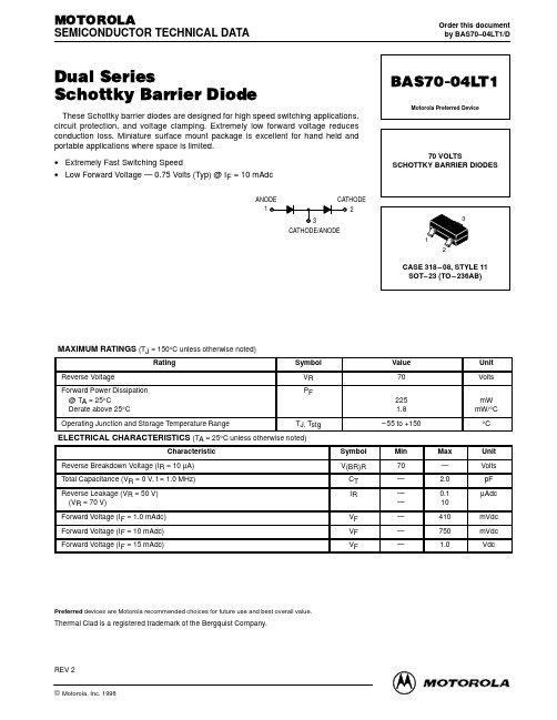
BAS70-04LT1
Motorola Preferred Device
70 VOLTS SCHOTTKY BARRIER DIODES
3 1 2
CASE 318 – 08, STYLE 11 SOT– 23 (TO – 236AB)
The 556°C/W for the SOT–23 package assumes the use of the recommended footprint on a glass epoxy printed circuit board to achieve a power dissipation of 225 milliwatts. There are other alternatives to achieving higher power dissipation from the SOT–23 package. Another alternative would be to use a ceramic substrate or an aluminum core board such as Thermal Clad™. Using a board material such as Thermal Clad, an aluminum core board, the power dissipation can be doubled using the same footprint.
MINIMUM RECOMMENDED FOOTPRINT FOR SURFACE MOUNTED APPLICATIONS
Surface mount board layout is a critical portion of the total design. The footprint for the semiconductor packages must be the correct size to insure proper solder connection interface between the board and the package. With the correct pad geometry, the packages will self align when subjected to a solder reflow process.
BAS70L中文资料

BAS70L
This data sheet contains data from the objective specification for product development. Philips Semiconductors reserves the right to change the specification in any manner without notice. This data sheet contains data from the preliminary specification. Supplementary data will be published at a later date. Philips Semiconductors reserves the right to change the specification without notice, in order to improve the design and supply the best possible product. This data sheet contains data from the product specification. Philips Semiconductors reserves the right to make changes at any time in order to improve the design, manufacturing and supply. Relevant changes will be communicated via a Customer Product/Process Change Notification (CPCN).
PACKAGE OUTLINE Leadless ultra small plastic package; 2 terminals; body 1.0 x 0.6 x 0.5 mm
安全技术说明书 Covi-ox T-70 EU

安全技术说明书页: 1/10 巴斯夫安全技术说明书日期 / 修订: 24.10.2016版本: 2.0产品: Covi-ox® T-70 EU(30533886/SDS_GEN_CN/ZH)印刷日期 03.11.20231. 物质/制剂及公司信息Covi-ox® T-70 EU推荐用途和限制用途: 抗氧化剂, 食品工业公司:巴斯夫(中国)有限公司中国上海浦东江心沙路300号邮政编码 200137电话: +86 21 20391000传真号: +86 21 20394800E-mail地址: **********************紧急联络信息:巴斯夫紧急热线中心(中国)+86 21 5861-1199巴斯夫紧急热线中心(国际):电话: +49 180 2273-112Company:BASF (China) Co., Ltd.300 Jiang Xin Sha RoadPu Dong Shanghai 200137, CHINA Telephone: +86 21 20391000Telefax number: +86 21 20394800E-mail address: ********************** Emergency information:Emergency Call Center (China):+86 21 5861-1199International emergency number: Telephone: +49 180 2273-1122. 危险性识别纯物质和混合物的分类:根据 GHS 标准,该产品不需要进行分类。
标签要素和警示性说明:根据GHS标准,该产品不需要添加危险警示标签巴斯夫安全技术说明书日期 / 修订: 24.10.2016版本: 2.0产品: Covi-ox® T-70 EU(30533886/SDS_GEN_CN/ZH)印刷日期 03.11.2023其它危害但是不至于归入分类:产品渗漏/溢出有高度致滑危险。
BAS70-06-HT3资料
BAS70-HT3 to BAS70-06-HT3Document Number 85689Rev. 1.3, 15-Apr-04Vishay Semiconductors1Small Signal Schottky Diodes, Single & DualFeatures•These diodes feature very low turn-on voltage and fast switching.•These devices are protected by a PNjunction guard ring against excessive voltage, such as electrostatic discharges. •Space saving LLP package •Lead (Pb)-free component•Component in accordance to RoHS 2002/95/EC and WEEE 2002/96/ECMechanical DataCase: LLP75-3B Plastic caseMolding Compound Flammability Rating:UL 94 V-0Terminals: High temperature soldering guaranteed:260°C/10 sec. at terminals Weight: approx. 5.2 mgParts TableAbsolute Maximum RatingsT amb = 25°C, unless otherwise specifiedThermal CharacteristicsT amb = 25°C, unless otherwise specifiedPartOrdering codeMarkingRemarksBAS70-HT3BAS70-HT3-GS0873T ape and Reel BAS70-04-HT3BAS70-04-HT3-GS0874T ape and Reel BAS70-05-HT3BAS70-05-HT3-GS0875T ape and Reel BAS70-06-HT3BAS70-06-HT3-GS0876T ape and ReelParameterT est conditionSymbol Value Unit Repetitive peak reverse voltage V RRM 70V Forward continuous current T amb = 25°C I F 200mA Surge forward current t p < 1 s, T amb = 25°C I FSM 600mA Power dissipationT amb = 25°CP tot200mWParameterT est conditionSymbol Value Unit Thermal resistance junction to ambient airR thJA 430°C Junction temperature T j 125°C Storage temperature rangeT S- 55 to +125°C 2Document Number 85689Rev. 1.3, 15-Apr-04BAS70-HT3 to BAS70-06-HT3Vishay Semiconductors Electrical CharacteristicsT amb = 25°C, unless otherwise specifiedPackage Dimensions in mm (Inches)ParameterTest conditionSymbol Min Typ.MaxUnit Reverse breakdown voltage I R = 10 µA (pulsed)V (BR)R 70V Leakage current V R = 50 V , t p < 300 µs I R 20100nA Forward voltage t p < 300 µs, I F = 1.0 mA V F 410mV t p < 300 µs, I F = 15 mA V F 1000mV Diode capacitance V R = 0 V , f = 1 MHz C tot 1.52pF Reverse recovery timeI F = 10 mA, I R = 10 mA, I rr = 1 mA, R L = 100 Ωt rr5nsBAS70-HT3 to BAS70-06-HT3Document Number 85689Rev. 1.3, 15-Apr-04Vishay Semiconductors3Ozone Depleting Substances Policy StatementIt is the policy of Vishay Semiconductor GmbH to1.Meet all present and future national and international statutory requirements.2.Regularly and continuously improve the performance of our products, processes, distribution and operating systems with respect to their impact on the health and safety of our employees and the public, as well as their impact on the environment.It is particular concern to control or eliminate releases of those substances into the atmosphere which are known as ozone depleting substances (ODSs).The Montreal Protocol (1987) and its London Amendments (1990) intend to severely restrict the use of ODSs and forbid their use within the next ten years. Various national and international initiatives are pressing for an earlier ban on these substances.Vishay Semiconductor GmbH has been able to use its policy of continuous improvements to eliminate the use of ODSs listed in the following documents.1.Annex A, B and list of transitional substances of the Montreal Protocol and the London Amendments respectively2.Class I and II ozone depleting substances in the Clean Air Act Amendments of 1990 by the Environmental Protection Agency (EPA) in the USA3.Council Decision 88/540/EEC and 91/690/EEC Annex A, B and C (transitional substances) respectively.Vishay Semiconductor GmbH can certify that our semiconductors are not manufactured with ozone depleting substances and do not contain such substances.We reserve the right to make changes to improve technical designand may do so without further notice.Parameters can vary in different applications. All operating parameters must be validated for each customer application by the customer. Should the buyer use Vishay Semiconductors products for any unintended or unauthorized application, the buyer shall indemnify Vishay Semiconductors against all claims, costs, damages, and expenses, arising out of, directly or indirectly, any claim of personaldamage, injury or death associated with such unintended or unauthorized use.Vishay Semiconductor GmbH, P.O.B. 3535, D-74025 Heilbronn, GermanyLegal Disclaimer NoticeVishay Document Number: Revision: 08-Apr-051NoticeSpecifications of the products displayed herein are subject to change without notice. Vishay Intertechnology, Inc., or anyone on its behalf, assumes no responsibility or liability for any errors or inaccuracies.Information contained herein is intended to provide a product description only. No license, express or implied, by estoppel or otherwise, to any intellectual property rights is granted by this document. Except as provided in Vishay's terms and conditions of sale for such products, Vishay assumes no liability whatsoever, and disclaims any express or implied warranty, relating to sale and/or use of Vishay products including liability or warranties relating to fitness for a particular purpose, merchantability, or infringement of any patent, copyright, or other intellectual property right. The products shown herein are not designed for use in medical, life-saving, or life-sustaining applications. Customers using or selling these products for use in such applications do so at their own risk and agree to fully indemnify Vishay for any damages resulting from such improper use or sale.。
涂料油墨水染色用进口蓝色染料溶剂蓝70

涂料油墨水染料用进口蓝色染料溶剂蓝70染色用进口蓝色溶剂染料蓝70为金属络合染料,颜色鲜艳、易溶解使用。
有高着色、高浓度、高耐候、耐温耐光、耐酸碱等特点,耐渗色为4-5级,使用的过程中不易出现褪色、不易出现麻点等情况。
染料类别:酞菁类染料。
铝箔纸、烫金、喷墨、马克笔文具墨水、真空电镀膜等染色用色泽鲜艳的蓝色染料SB70具体指标如下:C. I. Generic Name :Solvent Blue 70Appearance ------ Bright Blue PowderHue ------ BlueMelting Point ------ 175 ~ 180 ℃Moisture ------ 5.0 % maxpH of Water Extraction ------ 5.5 ~ 7.5Solubility ------Insoluble in Water. Soluble in Organic solvent.Application :Gravure Ink and the other Solvent Type Ink. Wood stain. Printing Ink for Aluminum Foil and Metalized Film. Writing and Marking Ink. etc.Packing Unit ------ 5 ㎏/Carton Box, 20kgs/Carton Box.Storage ------ Stored in cool and dry place, keep container tightlyclosed, store away from heat, spark and flame.以上为进口金属络合染料溶剂蓝70天蓝色透明染料蓝基本数据参考。
注:以上数据仅供使用时参考,批量使用前,应对产品进行测试后方可使用。
高透明度进口染料蓝70的适合应用领域上端作者与您共同学习:木器着色、烫印材料、玻璃漆、皮革染色、鞋油染色、塑料喷涂、印刷油墨、文具油墨、金属喷涂、包装纸张盒、铝箔纸,真空电镀之PET及OPP塑胶薄膜等着色。
DIODES美台Schottky二极管BAS70选型手册
BAS70/ -04/ -05/ -06
Document number: DS11007 Rev. 24 - 2
2 of 5
August 2014
© Diodes Incorporated
PD, POWER DISSIPATION (mW)
250
Note 6
Notes: 6. Part mounted on FR-4 board with recommended pad layout, which can be found on our website at /datasheets/ap02001.pdf. 7. Short duration pulse test used to minimize self-heating effect.
Characteristic Peak Repetitive Reverse Voltage Working Peak Reverse Voltage DC Blocking Voltage
RMS Reverse Voltage Maximum Forward Continuous Current (Note 6) Non-Repetitive Peak Forward Surge Current @ t ≤ 1.0s
BAS70/ -04/ -05/ -06
SURFACE MOUNT SCHOTTKY BARRIER DIODE
Features and Benefits
• Low Turn-On Voltage • Fast Switching • PN Junction Guard Ring for Transient and ESD Protection • Totally Lead-Free & Fully RoHS Compliant (Notes 1 & 2) • Halogen and Antimony Free. “Green” Device (Note 3) • Qualified to AEC-Q101 Standards for High Reliability
BAS70-07中文资料

BAS70-07®June 1999 - Ed: 2ASMALL SIGNAL SCHOTTKY DIODEVERY SMALL CONDUCTION LOSSES NEGLIGIBLE SWITCHING LOSSES LOW FORWARD VOLTAGE DROP LOW THERMAL RESISTANCE EXTREMELY FAST SWITCHING SURFACE MOUNTED DEVICE FEATURES AND BENEFITSLow turn-on and high breakdown voltage diodes intended forultrafast switching and UHF detectors in hybrid mi-cro circuits. Packaged in SOT-143, this device is intended for surface mounting. Its dual inde-pendent diodes configuration makes it very inter-esting for applications where high integration is searched.DESCRIPTIONSOT-143Symbol ParameterValue Unit V RRM Repetitive peak reverse voltage 70V I F Continuous forward current 15mA I FSM Surge non repetitive forward current tp = 10ms 1A P tot Power Dissipation (note 1)T amb = 25°C310mW T stg Storage temperature range- 65 to +150°C Tj Maximum operating junction temperature *150°C TLMaximum temperature for soldering during 10s260°CNote 1: Ptot is the total dissipation of both diodes.ABSOLUTE RATINGS (limiting values)K1K2A1A2K1A1K2A2Symbol ParameterValue Unit R th (j-a)Junction to ambient (*)400°C/W(*) Mounted on epoxy board with recommended pad layout.THERMAL RESISTANCE * :dPtot dTj< 1Rth (j −a ) thermal runaway condition for a diode on its own heatsink1/4Symbol Tests Conditions Tests Conditions Min.Typ.Max.Unit V F *Forward voltage dropTj = 25°CI F = 1 mA 410mV I F = 10 mA 750mV I F = 15 mA1V V BR Breakdown voltage Tj = 25°C I R = 10 µA 70VI R **Reverse leakage currentTj = 25°CV R = 50 V 200nA V R = 70 V10µASTATIC ELECTRICAL CHARACTERISTICS Symbol Parameters Tests Conditions Min.Typ.Max.Unit C Junction capacitance V R = 1 V F = 1 MHz 2pF t rr Reverse recovery time I F = 10 mA Irr = 1 mA I R = 10 mA R L = 100 Ω5ns τEffective carrier lifetimeI F = 5 mA Krakauer method100psDYNAMIC CHARACTERISTICS (Tj = 25 °C)010203040506070800.000.020.040.060.080.100.120.140.160.18PF(av)(W)IF(av) (mA)δ= 0.2δ= 0.5δ= 1δ= 0.05δ= 0.1Tδ=tp/TtpFig.1 : Average forward power dissipation versus average forward current.2550751001251501020304050607080IF(mA)Tamb(°C)Fig.2 : Continuous forward current versus ambient temperature.Pulse test:* tp = 380 µs, δ < 2%** tp = 5 ms, δ < 2%BAS70-072/41E-31E-21E-11E+00.000.050.100.150.200.250.30IM(A)T a=50°CT a=25°CT a=100°Ct(s)I Mtδ=0.5Fig.3 : Non repetitive surge peak forward current versus overload duration (maximum values).5101520253035404550556065701E-31E-21E-11E+01E+1IR(µA)Tj=25°CTj=100°CVR(V)Fig.5 : Reverse leakage current versus reverse voltage applied (typical values).1E-31E-21E-11E+01E+11E+20.010.101.00Zth(j-a)/Rth(j-a)tp(s)Tδ=tp/Ttpδ= 0.1δ= 0.2δ= 0.5Single pulseFig.4 : Relative variation of thermal impedance junction to ambient versus pulse duration (alumine substrate 10mm x 8mm x 0.5mm).2550751001251E-21E-11E+01E+11E+2IR(µA)VR=70VTj(°C)Fig.6 : Reverse leakage current versus junction temperature (typical values).1101000.11.02.0VR(V)C(pF)F=1MHz Tj=25°CFig.7 : Junction capacitance versus reverse voltage applied (typical values).0.00.20.40.60.8 1.0 1.2 1.4 1.6 1.8 2.01E-41E-31E-27E-2IFM(A)Tj=100°C T ypical valuesTj=25°C Maximum valuesTj=25°C T ypical valuesVFM(V)Fig.8 : Forward voltage drop versus forward current.BAS70-073/4Information furnished is believed to be accurate and reliable. However, STMicroelectronics assumes no responsibility for the consequences of use of such information nor for any infringement of patents or other rights of third parties which may result from its use. No license is granted by implication or otherwise under any patent or patent rights of STMicroelectronics. Specifications mentioned in this publication are subject to change without notice. This publication supersedes and replaces all information previously supplied.STMicroelectronics products are not authorized for use as critical components in life support devices or systems without express written ap-proval of STMicroelectronics.The ST logo is a registered trademark of STMicroelectronics © 1999 STMicroelectronics - Printed in Italy - All rights reserved.STMicroelectronics GROUP OF COMPANIESAustralia - Brazil - China - Finland - France - Germany - Hong Kong - India - Italy - Japan - MalaysiaMalta - Morocco - Singapore - Spain - Sweden - Switzerland - United Kingdom - U.S.A.PACKAGE MECHANICAL DATA SOT-143ALCD EHe2bb1e1A1REF.DIMENSIONSMillimeters Inches Min.Max.Min.Max.A0.8 1.20.03140.0472A10.010.1270.00040.005b 0.350.60.0140.024b10.550.950.0220.037C 0.0850.20.0030.008D 2.8 3.040.110.12E 1.21.40.0470.055e11.90 Typ.0.075 Typ.e20.2 Typ.0.008 Typ.H2.12.640.0830.103L0.55 Typ.0.022 Typ.FOOTPRINT DIMENSIONS (millimeters)Type Marking Package Weight Base qty Delivery mode BAS70-07D99SOT-1430.01g.3000Tape & reelMARKING1.920.952.251.10.650.2BAS70-074/4。