AD8619ARUZ-REEL中文资料
AD8692ARMZ-REEL中文资料
Supply Current/Amplifier
DYNAMIC PERFORMANCE Slew Rate Settling Time Gain Bandwidth Product Phase Margin Total Harmonic Distortion + Noise
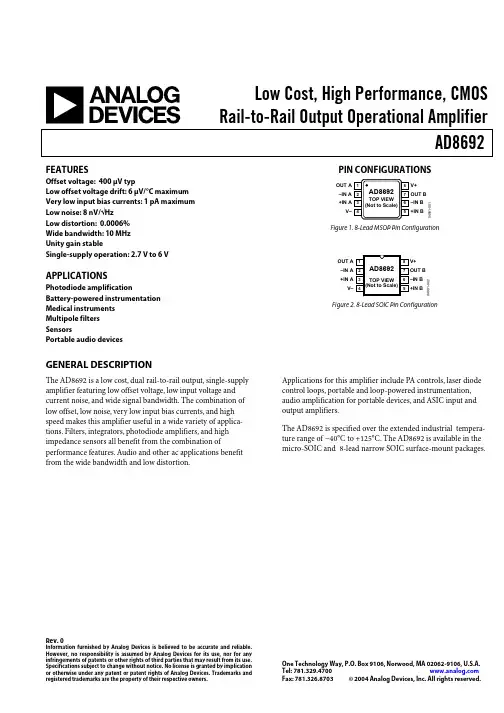
Applications for this amplifier include PA controls, laser diode control loops, portable and loop-powered instrumentation, audio amplification for portable devices, and ASIC input and output amplifiers.
REVISION HISTORY 10/04—Revision 0: Initial Version
Typical Performance Characteristics ..............................................6 Outline Dimensions ....................................................................... 11
Conditions
VCM = −0.3 V to +1.6 V VCM = −0.1 V to +1.6 V; −40°C < TA < +125°C
AD9860资料
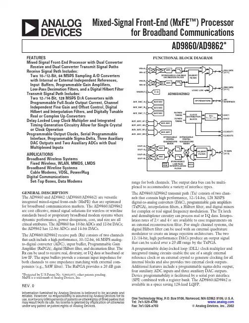
REV.0aInformation furnished by Analog Devices is believed to be accurate and reliable. However, no responsibility is assumed by Analog Devices for its use, nor for any infringements of patents or other rights of third parties that may result from its use. No license is granted by implication or otherwise under any patent or patent rights of Analog Devices.One Technology Way, P.O. Box 9106, Norwood, MA 02062-9106, U.S.A.Tel: 781/ Fax: 781/326-8703© Analog Devices, Inc., 2002AD9860/AD9862*Mixed-Signal Front-End (MxFE ™) Processorfor Broadband Communications*Protected by U.S.Patent No. 5,969,657; other patents pending.MxFE is a trademark of Analog Devices, Inc.GENERAL DESCRIPTIONThe AD9860 and AD9862 (AD9860/AD9862) are versatile integrated mixed-signal front-ends (MxFE) that are optimized for broadband communication markets. The AD9860/AD9862are cost effective, mixed signal solutions for wireless or wireline standards based or proprietary broadband modem systems where dynamic performance, power dissipation, cost, and size are all critical attributes. The AD9860 has 10-bit ADCs and 12-bit DACs;the AD9862 has 12-bit ADCs and 14-bit DACs.The AD9860/AD9862 receive path (Rx) consists of two channels that each include a high performance, 10-/12-bit, 64 MSPS analog-to-digital converter (ADC), input buffer, Programmable Gain Amplifier (RxPGA), digital Hilbert filter, and decimation filter. The Rx can be used to receive real, diversity, or I/Q data at baseband or low IF. The input buffers provide a constant input impedance for both channels to ease impedance matching with external com-ponents (e.g., SAW filter). The RxPGA provides a 20dB gainrange for both channels. The output data bus can be multi-plexed to accommodate a variety of interface types.The AD9860/AD9862 transmit path (Tx) consists of two chan-nels that contain high performance, 12-/14-bit, 128 MSPS digital-to-analog converters (DAC), programmable gain amplifiers (TxPGA), interpolation filters, a Hilbert filter, and digital mixers for complex or real signal frequency modulation. The Tx latch and demultiplexer circuitry can process real or I/Q data. Interpo-lation rates of 2ϫ and 4ϫ are available to ease requirements on an external reconstruction filter. For single channel systems, the digital Hilbert filter can be used with an external quadrature modulator to create an image rejection architecture. The two 12-/14-bit, high performance DACs produce an output signal that can be scaled over a 20 dB range by the TxPGA.A programmable delay-locked loop (DLL) clock multiplier and integrated timing circuits enable the use of a single external reference clock or an external crystal to generate clocking for all internal blocks and also provides two external clock outputs.Additional features include a programmable sigma-delta output,four auxiliary ADC inputs and three auxiliary DAC outputs.Device programmability is facilitated by a serial port interface (SPI) combined with a register bank. The AD9860/AD9862 is available in a space saving 128-lead LQFP.FUNCTIONAL BLOCK DIAGRAMTx DA T A [0:13]SIGDEL T A T A FEATURESMixed-Signal Front-End Processor with Dual Converter Receive and Dual Converter Transmit Signal Paths Receive Signal Path Includes:Two 10-/12-Bit, 64 MSPS Sampling A/D Converters with Internal or External Independent References,Input Buffers, Programmable Gain Amplifiers,Low-Pass Decimation Filters, and a Digital Hilbert Filter Transmit Signal Path Includes:Two 12-/14-Bit, 128 MSPS D/A Converters with Programmable Full-Scale Output Current, Channel Independent Fine Gain and Offset Control, Digital Hilbert and Interpolation Filters, and Digitally Tunable Real or Complex Up-ConvertersDelay-Locked Loop Clock Multiplier and Integrated Timing Generation Circuitry Allow for Single Crystal or Clock OperationProgrammable Output Clocks, Serial Programmable Interface, Programmable Sigma-Delta, Three Auxiliary DAC Outputs and Two Auxiliary ADCs with Dual Multiplexed InputsAPPLICATIONSBroadband Wireless SystemsFixed Wireless, WLAN, MMDS, LMDS Broadband Wireline SystemsCable Modems, VDSL, PowerPlug Digital CommunicationsSet-Top Boxes, Data ModemsAD9860/AD9862–SPECIFICATIONS(V A = 3.3 V ؎ 5%, V D = 3.3 V ؎ 10%, f DAC = 128 MHz, f ADC = 64 MHzNormal Timing Mode, 2؋ DLL Setting, R SET = 4 k⍀, 50 ⍀ DAC Load,–2–REV. 0AD9860/AD9862–3–Test AD9860/AD9862Rx PARAMETERS (continued)Temp Level Min Typ Max Unit DC ACCURACYDifferential Nonlinearity25ºC III±0.3/±0.4LSB Integral Nonlinearity25ºC III±1.2/±5LSB Offset Error25ºC III±0.1%FSR Gain Error25ºC III±0.2%FSR Aperture Delay25ºC III 2.0ns Aperture Uncertainty (Jitter)25ºC III 1.2ps rms Input Referred Noise25ºC III 250µV Reference Voltage ErrorREFT-REFB Error (1 V)25ºC I±1±4mV AD9860 DYNAMIC PERFORMANCE (A IN = –0.5 dBFS, f = 5 MHz)Signal-to-Noise Ratio25∞C I59.0 60.66dBc Signal-to-Noise and Distortion Ratio25∞C I56.0 58.0dBc Total Harmonic Distortion25∞C I–76.5–70.5dBc Spurious Free Dynamic Range25∞C I70.3 81.0dBc AD9862 DYNAMIC PERFORMANCE (A IN = –0.5 dBFS, f = 5 MHz)Signal-to-Noise Ratio25∞C I62.6 64.2dBc Signal-to-Noise and Distortion Ratio25∞C I62.5 64.14dBc Total Harmonic Distortion25∞C I–79.22–73.2dBc Spurious Free Dynamic Range25∞C I77.09 85.13dBc CHANNEL-TO-CHANNEL ISOLATIONTx-to-Rx (A OUT = 0 dBFS, f OUT = 7 MHz)25ºC III >90dB Rx Channel Crosstalk (f1 = 6 MHz, f2 = 9 MHz)25ºC III >80dB PARAMETERSCMOS LOGIC INPUTSLogic “1” Voltage, V IH25ºC II DRVDD – 0.7V Logic “0” Voltage, V IL25ºC II0.4V Logic “1” Current25ºC II12µA Logic “0” Current25ºC II12µA Input Capacitance25ºC III 3pF CMOS LOGIC OUTPUTS (1 mA Load)Logic “1” Voltage, V OH25ºC II DRVDD – 0.6V Logic “0” Voltage, V OL25ºC II0.4V POWER SUPPLYAnalog Supply CurrentsTx (Both Channels, 20 mA FS Output)25ºC I 7076mA Tx Powered Down25ºC I 2.5 5.0mA Rx (Both Channels, Input Buffer Enabled)25ºC I 275307mA Rx (Both Channels, Input Buffer Disabled)25ºC III 245mA Rx (32 MSPS, Low Power Mode, Buffer Disabled)25ºC III 155mA Rx (16 MSPS, Low Power Mode, Buffer Disabled)25ºC III 80mA Rx Path Powered Down25ºC I 5.0 6.0mA DLL25ºC III 12mA Digital Supply CurrentAD9860 Both Rx and Tx Path (All Channels Enabled)2ϫ Interpolation, f DAC = f ADC = 64 MSPS25ºC I 92112mA AD9862 Both Rx and Tx Path (All Channels Enabled)2ϫ Interpolation, f DAC = f ADC = 64 MSPS25ºC I 104124mA Tx Path (f DAC = 128 MSPS)Processing Blocks Disabled25ºC III 45mA 4ϫ Interpolation25ºC III 90mA 4ϫ Interpolation, Coarse Modulation25ºC III 110mA 4ϫ Interpolation, Fine Modulation25ºC III 110mA 4ϫ Interpolation, Coarse and Fine Modulation25ºC III 130mAREV. 0REV. 0–4–AD9860/AD9862Test AD9860/AD9862(20 pF Load)Temp Level Min Typ MaxUnit Minimum Reset Pulsewidth Low (t RL )NA NA 5Clock Cycles Digital Output Rise/Fall Time 25ºC III 2.84ns DLL Output Clock25ºC III 32128MHz DLL Output Duty Cycle25ºC III 50%Tx –/Rx –Interface (See Figures 11 and 12)TxSYNC/TxIQ Setup Time (t Tx1, t Tx3)25ºC III 3ns TxSYNC/TxIQ Hold Time (t Tx2, t Tx4)25ºC III 3ns RxSYNC/RxIQ/IF to Valid Time(t Rx1, t Rx3)25ºC III 5.2ns RxSYNC/RxIQ/IF Hold Time (t Rx2, t Rx4)25ºC III 0.2ns Serial Control Bus (See Figures 1 and 2)Maximum SCLK Frequency (f SCLK )Full III 16MHz Minimum Clock Pulsewidth High (t HI )Full III 30ns Minimum Clock Pulsewidth Low (t LOW )Full III 30ns Maximum Clock Rise/Fall TimeFull III 1ms Minimum Data/SEN Setup Time (t S )Full III 25ns Minimum SEN/Data Hold Time (t H )Full III 0ns Minimum Data/SCLK Setup Time (t DS )Full III 25ns Minimum Data Hold Time (t DH )Full III 0ns Output Data Valid/SCLK Time (t DV )Full III 30ns AUXILARY ADC Conversion Rate 25ºC III 1.25MHz Input Range 25ºC III 3V Resolution 25ºC III 10Bits AUXILARY DAC Settling Time 25ºC III 8m s Output Range 25ºC III 3V Resolution25ºC III 8Bits ADC TIMINGLatency (All Digital Processing Blocks Disabled)25ºC III 7Cycles DAC TimingLatency (All Digital Processing Blocks Disabled)25ºC III 3Cycles Latency (2ϫ Interpolation Enabled)25ºC III 30Cycles Latency (4ϫ Interpolation Enabled)25ºC III 72Cycles Additional Latency (Hilbert Filter Enabled)25ºC III 36Cycles Additional Latency (Coarse Modulation Enabled)25ºC III 5Cycles Additional Latency (Fine Modulation Enabled)25ºC III 8Cycles Output Settling Time (TST) (to 0.1%)25ºCIII35nsSpecifications subject to change without notice.TIMING CHARACTERISTICSTest AD9860/AD9862PARAMETERS (continued)TempLevelMinTyp MaxUnitPOWER SUPPLY (continued)Rx Path (f ADC = 64 MSPS)Processing Blocks Disabled 25ºCIII 9mA Decimation Filter Enabled 25ºC III 15mA Hilbert Filter Enabled25ºC III 16mA Hilbert and Decimation Filter Enabled25ºC III 18.5mANOTES 1% f DATA refers to the input data rate of the digital block.2Interpolation filter stop band is defined by image suppression of 50 dB or greater.Specifications subject to change without notice.REV. 0AD9860/AD9862–5–CAUTIONESD (electrostatic discharge) sensitive device. Electrostatic charges as high as 4000V readily accumulate on the human body and test equipment and can discharge without detection. Although the AD9860/AD9862 features proprietary ESD protection circuitry, permanent damage may occur on devices subjected to high energy electrostatic discharges. Therefore, proper ESD precautions arerecommended to avoid performance degradation or loss of functionality.ABSOLUTE MAXIMUM RATINGS 1Power Supply (V AS , V DS ) . . . . . . . . . . . . . . . . . . . . . . . . .3.9 V Digital Output Current . . . . . . . . . . . . . . . . . . . . . . . . . .5 mA Digital Inputs . . . . . . . . . . . . . . . .–0.3 V to DRVDD + 0.3 V Analog Inputs . . . . . . . . . . . . . .–0.3 V to AVDD (IQ) + 0.3 V Operating Temperature 2 . . . . . . . . . . . . . . . . .–40؇C to +70؇C Maximum Junction Temperature . . . . . . . . . . . . . . . . .150؇C Storage Temperature . . . . . . . . . . . . . . . . . . .–65؇C to +150؇C Lead Temperature (Soldering 10 sec) . . . . . . . . . . . . . .300؇CNOTES 1Absolute maximum ratings are limiting values, to be applied individually, and beyond which the serviceability of the circuit may be impaired. Functional operability under any of these conditions is not necessarily implied. Exposure to absolute maximum rating conditions for extended periods of time may affect device reliability.2The AD9860/AD9862 have been characterized to operate over the industrial temperature range (–40؇C to +85؇C) when operated in Half Duplex Mode.EXPLANATION OF TEST LEVELSI.Devices are 100% production tested at 25ºC and guaranteed by design and characterization testing for the extended industrial temperature range (–40ºC to +70ºC).II.Parameter is guaranteed by design and/or characterization testing.III.Parameter is a typical value only.NA.Test level definition is not applicable.THERMAL CHARACTERISTICS Thermal Resistance128-Lead LQFP JA = 29ºC/WORDERING GUIDEModel Temperature Range Package DescriptionPackage Option AD9860BST –40∞C to +70∞C *128-Lead Low Profile Plastic Quad Flatpack (LQFP) ST-128B AD9862BST –40∞C to +70∞C *128-Lead Low Profile Plastic Quad Flatpack (LQFP) ST-128BAD9860PCB Evaluation Board with AD9860AD9862PCBEvaluation Board with AD9862*The AD9860/AD9862 have been characterized to operate over the industrial temperature range (–40؇C to +85؇C) when operated in Half Duplex Mode.REV. 0–6–AD9860/AD9862PIN CONFIGURATIONAGND AVDD DVDD DGND DGND DVDD Tx11/13 (MSB)Tx10/12T x 9/1T x 8/1T x 7/T x 6/T x 5/T x 4/T x 3/T x 2/T x 1/T x 0/N C /T x N C /T x AUX_ADC_A1AGND AVDD AVDD SIGDEL T AUX_DAC_A AUX_DAC_B AUX_DAC_CAGNDDLL_Lock AGND NC AVDD OSC1OSC2AGND CLKSEL AVDD AGND AVDD REFIO FSADJ AVDD AGND IOUT–A IOUT+A AGND AGND IOUT+B IOUT–B T x S Y N D G N D V D S C L S D S D I S E D G N D V D D G N D V D M O D E /T x B L A N R E S E T C L K O U T A G N DA V D DA V D DA G N DV I N +BV I N –BA G N DA G N DV R E FA G N DA G N DV I N –AV I N +AA G N DA V D DA V D DA G N DR E F B _AR E F T _AA G N DA V D DA V D DA U X _A D C _B 2A U X _A D C _B 1A U X _A D C _R E FA U X _A D C _A 2NC = NO CONNECTAD9860/AD9862–7–Pin No.Mnemonic FunctionClock Pins10DLL_Lock DLL Lock Indicator Pin11, 16AGND DLL Analog Ground Pins12NC No Connect13AVDD DLL Analog Supply Pin14OSC1Single Ended Input Clock(or Crystal Oscillator Input)15OSC2Crystal Oscillator Input17CLKSEL Controls CLKOUT1 Rate64CLKOUT2Clock Output Generated from InputClock (DLL Multiplier Settingand CLKOUT2 Divide Factor)65CLKOUT1Clock Output Generated fromInput Clock (1ϫ if CLKSEL = 1or /2 if CLKSEL = 0)Various Pins1AUX_ADC_A1Auxiliary ADC A Input 13, 4, 13AVDD Analog Power Pins2, 9AGND Analog Ground Pins5SIGDELT Digital Output fromProgrammable Sigma-Delta6AUX_DAC_A Auxiliary DAC A Output7AUX_DAC_B Auxiliary DAC B Output8AUX_DAC_C Auxiliary DAC C Output33, 36, 53,DVDD Digital Power Supply Pin59, 61, 66,9334, 35, 52,DGND Digital Ground Pin58, 60, 67,9454SCLK Serial Bus Clock Input55SDO Serial Bus Data Bit56SDIO Serial Bus Data Bit57SEN Serial Bus Enable63RESETB Reset (SPI Registers and Logic) 95AUX_SPI_do Optional Auxiliary ADC Serial BusData Out Bit96AUX_SPI_clk Optional Auxiliary ADC Serial BusData Out Latch Clock97AUX_SPI_csb Optional Auxiliary ADC Serial BusChip Select Bit128AUX_ADC_A2Auxiliary ADC A Input 2126AUX_ADC_B1Auxiliary ADC B Input 1125AUX_ADC_B2Auxiliary ADC B Input 2127AUX_ADC_REF Auxiliary ADC ReferencePin No.Mnemonic FunctionReceive Pins68/70–79D0A to10-/12-Bit ADC Output ofD9A/D11A Receive Channel A80/82–91D0B to10-/12-Bit ADC Output ofD9B/D11B Receive Channel B92RxSYNC Synchronization Clock forChannel A and Channel B Rx Paths98, 99,AVDD Analog Supply Pins104, 105,117, 118,123, 124,100, 103,AGND Analog Ground Pins106, 109,110, 112,113, 116,119, 122,101REFT_B Top Reference Decoupling forChannel B ADC102REFB_B Bottom Reference Decouplingfor Channel B ADC107VIN+B Receive Channel B Differential (+) Input108VIN–B Receive Channel B Differential (؊) Input111VREF Internal ADC Voltage Reference114VIN–A Receive Channel A Differential (؊) Input115VIN+A Receive Channel A Differential (+) Input120REFB_A Bottom Reference Decoupling forChannel A ADC121REFT_A Top Reference Decoupling forChannel A ADCTransmit Pins18, 20AVDD Analog Supply Pins23, 3219, 24,AGND Analog Ground Pins27, 28, 3121REFIO Reference Output, 1.2 V Nominal22FSADJ Full-Scale Current Adjust25IOUT–A Transmit Channel A DACDifferential (؊) Output26IOUT+A Transmit Channel A DACDifferential (+) Output29IOUT+B Transmit Channel B DACDifferential (+) Output30IOUT–B Transmit Channel B DACDifferential (؊) Output37–48/50Tx11/Tx1312-/14-Bit Transmit DAC Datato Tx0(Interleaved Data when Required)51TxSYNC Synchronization Input for Transmitter62MODE/Configures Default Timing Mode,TxBLANK*Controls Tx Digital Power Down*The logic level of the Mode/TxBLANK pin at power up defines the default timingmode; a logic low configures Normal Operation, logic high configures AlternateOperation Mode.PIN FUNCTION DESCRIPTIONSREV. 0AD9860/AD9862DEFINITIONS OF SPECIFICATIONSDifferential Nonlinearity Error (DNL, No Missing Codes)An ideal converter exhibits code transitions that are exactly 1LSB apart. DNL is the deviation from this ideal value. Guaranteed no missing codes to 10-bit resolution indicate that all 1024 codes respectively, must be present over all operating ranges.Integral Nonlinearity Error (INL)Linearity error refers to the deviation of each individual code from a line drawn from “negative full scale” through “positive full scale.” The point used as “negative full scale” occurs 1/2LSB before the first code transition. “Positive full scale” is defined as a level 1 1/2 LSB beyond the last code transition. The deviation is measured from the middle of each particular code to the true straight line.Phase NoiseSingle-sideband phase noise power is specified relative to the carrier (dBc/Hz) at a given frequency offset (1 kHz) from the carrier. Phase noise can be measured directly in Single Tone Trans-mit Mode with a spectrum analyzer that supports noise marker measurements. It detects the relative power between the carrier and the offset (1 kHz) sideband noise and takes the resolution bandwidth (rbw) into account by subtracting 10 log(rbw). It also adds a correction factor that compensates for the implementation of the resolution bandwidth, log display, and detector characteristic. Output Compliance RangeThe range of allowable voltage at the output of a current-output DAC. Operation beyond the maximum compliance limits may cause either output stage saturation or breakdown, resulting in nonlinear performance.Spurious-Free Dynamic Range (SFDR)The difference, in dB, between the rms amplitude of the DAC’s output signal (or ADC’s input signal) and the peak spurious signal over the specified bandwidth (Nyquist bandwidth unless otherwise noted).Pipeline Delay (Latency)The number of clock cycles between conversion initiation and the associated output data being made available.Offset ErrorFirst transition should occur for an analog value 1/2 LSB above –full scale. Offset error is defined as the deviation of the actual transition from that point.Gain ErrorThe first code transition should occur at an analog value 1/2LSB above –full scale. The last transition should occur for an analog value 1 1/2 LSB below the nominal full scale. Gain error is the deviation of the actual difference between first and last code transitions and the ideal difference between first and last code transitions.Aperture DelayThe aperture delay is a measure of the Sample-and-Hold Ampli-fier (SHA) performance and specifies the time delay between the rising edge of the sampling clock input to when the input signal is held for conversion.Aperture Uncertainty (Jitter)Aperture jitter is the variation in aperture delay for successivesamples and is manifested as noise on the input to the ADC.Input Referred NoiseThe rms output noise is measured using histogram techniques.The ADC output code’s standard deviation is calculated in LSB and converted to an equivalent voltage. This results in a noisefigure that can be referred directly to the input of the AD9860/ AD9862.Signal-to-Noise and Distortion (S/N+D, SINAD) RatioS/N+D is the ratio of the rms value of the measured input signal to the rms sum of all other spectral components below the Nyquist frequency, including harmonics but excluding dc. The value for S/N+D is expressed in decibels.Effective Number of Bits (ENOB)For a sine wave, SINAD can be expressed in terms of the number of bits. Using the following formula:N=()SINAD dB–..176602it is possible to get a measure of performance expressed as N,the effective number of bits. Thus, effective number of bits fora device for sine wave inputs at a given input frequency can becalculated directly from its measured SINAD.Signal-to-Noise Ratio (SNR)SNR is the ratio of the rms value of the measured input signal to the rms sum of all other spectral components below the Nyquist frequency, excluding harmonics and dc. The value for SNR isexpressed in decibels.Total Harmonic Distortion (THD)THD is the ratio of the rms sum of the first six harmoniccomponents to the rms value of the measured input signal and is expressed as a percentage or in decibels.Power Supply RejectionPower supply rejection specifies the converter’s maximum full-scale change when the supplies are varied from nominal to minimum and maximum specified voltages.Channel-to-Channel Isolation (Crosstalk)In an ideal multichannel system, the signal in one channel will not influence the signal level of another channel. The channel-to-channel isolation specification is a measure of the change that occurs to a grounded channel as a full-scale signal is applied to another channel.REV. 0–8––9–FREQUENCY – MHzTPC 1.AD9862 Tx Output 6 MHzSingle Tone; CLKIN = 32 MHz;DLL 4ϫ SettingFREQUENCY – MHzMAGNITUDE–dBm–20–4020406080100110120–60–80140TPC 4.TxDAC Generating anOFDM Signal; CLKIN = 64 MHz,DLL 2ϫ Settingf OUT – MHz5203510152530THD–dBcTPC 7.TxDAC HarmonicDistortion vs. f OUTFREQUENCY – MHzTPC 2.AD9862 Tx Output 6 MHzSingle Tone; CLKIN = 64 MHz;DLL 2ϫ SettingFREQUENCY – MHzMAGNITUDE–dBm20406080100110120140TPC 5.TxDAC Generating anOFDM Signal; CLKIN = 64 MHz,DLL 2ϫ SettingFREQUENCY– MHzSNR–dB74737271706968TPC 8.Signal-to-Noise Ratio (SNR)vs. f OUTFREQUENCY – MHzTPC 3.AD9862 Tx Output 6 MHzSingle Tone; CLKIN = 128 MHz;DLL 1ϫ SettingFREQUENCY – MHzMAGNITUDE–dBm–20–40–60–80–100–120TPC 6.Zoomed in Plot of FourNotched Carriers of OFDM Signal;CLKIN = 64 MHz, DLL 2ϫ SettingCARRIER FREQUENCY – MHz5IMD–dBc20–60–65–70–75–80–85–9010152530–50–55–95TPC 9.Two Tone Intermodulationvs. f OUT1 (f OUT2 = f OUT1 + 1 MHz)REV. 0AD9860/AD9862FFT OUTPUT – MHz5FFTMAGNITUDE–dBFS20–20–40–60–8010152530–100–120TPC 10.ADC Dual Tone FFT withBuffer Tones at 4.5 MHz and 5.5 MHzf IN – MHz52TPC 13.AD9862 Rx SINADvs. fINat 64 MSPSf IN – MHzTPC 16.AD9860 Rx SINADvs. f IN at 64 MSPSFFT OUTPUT – MHz5FFTMAGNITUDE–dBFS20–20–40–60–8010152530–100–120TPC 11.ADC Dual Tone FFT withoutBuffer Tones at 4.5 MHz and 5.5 MHzf IN – MHzSINAD–dBcTPC 14.AD9862 Rx SINADvs. f IN at 32 MSPSf IN – MHzSINAD–dBc62TPC 17.AD9860 Rx SINADvs. f IN at 32 MSPSFFT OUTPUT – MHz5FFTMAGNITUDE–dBFS20–20–40–60–8010152530–100–120TPC 12.ADC Dual Tone FFT(undersampling) without BufferTones at 69.5 MHz and 70.5 MHzf IN – MHz020050SINAD–dBc150250100300TPC 15.AD9862 Rx SINADvs. f IN at 16 MSPSf IN – MHzSINAD–dBc62TPC 18.AD9860 Rx SINADvs. f IN at 16 MSPSREV. 0–10–AD9860/AD9862INPUT FREQUENCY – MHzT H D – d B c–60–65–70–75–80–85–90–50–55–95–100TPC 19.Rx THD vs. f IN ,F ADC = 64 MSPSINPUT FREQUENCY – MHzS F D R – d B c–60–65–70–75–80–85–90–50–55–95–100TPC 22.Rx SFDR @ 64 MSPSINPUT FREQUENCY – MHzR E L A T I V E A T T E N U A T I O N – d B10–1–2–3–4–5–6TPC 25.Rx Input Attenuationf IN – MHzT H D – d B c–75–80–85–90–70–65–60–55–50TPC 20.Rx THD vs. f IN ,F ADC = 32 MSPS f IN – MHzS F D R – d B c–75–80–85–90–70–65–60–55–50–95TPC 23.Rx SFDR @ 32 MSPS f IN – MHzI N P U T I M P E D A N C E – ⍀60250240230220210200190204080100270260180280TPC 26.Rx Input Buffer Impedance vs. f INf IN – MHzT H D – d B c–75–80–85–90–70–65–60–55–50TPC 21.Rx THD vs. f IN ,F ADC = 16 MSPSf IN – MHz020050S F D R – d B c–75–80–85–90–70150250100–65–60–55–50300–95TPC 24.Rx SFDR @ 16 MSPSf ADC – MSPS04010R x A N A L O G P O W E R – m W30020010004003050205006007008007060TPC 27.Rx Analog Power ConsumptionAD9860/AD9862REGISTER MAP (0x00–0x3F)1NOTES1When writing to a register with unassigned register bit(s), a logic low must be written to the unassigned bit(s). By default, after power up or RESET, all registers are set low, except for the bits in the shaded boxes, which are set high.2DecimalAD9860/AD9862REGISTER BIT DEFINITIONSREGISTER 0: GENERALBIT 7: SDIO BiDir (Bidirectional)Default setting is low, which indicates SPI serial port uses dedi-cated input and output lines (i.e., 4-wire interface), SDIO and SDO Pins, respectively. Setting this bit high configures the serial port to use the SDIO Pin as a bidirectional data pin.BIT 6: LSB FirstDefault setting is low, which indicates MSB first SPI Port Access Mode. Setting this bit high configures the SPI port access to LSB first mode.BIT 5: Soft ResetWriting a high to this register resets all the registers to their default values and forces the DLL to relock to the input clock. The Soft Reset Bit is a one shot register and is cleared immediately after the register write is completed.REGISTER 1: Rx PWRDWNBIT 7: V REF, diff (Power-Down)Setting this bit high will power down the ADC’s differential references (i.e., REFT and REFB).BIT 6: V REF (Power-Down)Setting this register bit high will power down the ADC reference circuit (i.e., V REF).BIT 5: Rx Digital (Power-Down)Setting this bit high will power down the digital section of the receive path of the chip. Typically, any unused digital blocks are automatically powered down.BIT 4/3: Rx Channel B/Rx Channel A (Power-Down)Either ADC or both ADCs can be powered down by setting the appropriate register bit high. The entire Rx channel is powered down, including the differential references, input buffer, and the internal digital block. The bandgap reference remains active for quick recovery.BIT 2/1: Buffer B/Buffer A (Power-Down)Setting either of these bits high will power down the input buffer circuits for the respective channel. The input buffer should be powered down when bypassed. By default, these bits are low and the input buffers are enabled.BIT 0: All Rx (Power-Down)Setting this bit high powers down all circuits related to the receive path.REGISTER 2/3: Rx A/Rx BBIT 7: Bypass Buffer A/Bypass Buffer BSetting either of these bits high will bypass the respective input buf-fer circuit. When the buffer is bypassed, the input signal is routed directly to the switched capacitor SHA input of the RxPGA. When operating with buffer bypassed, it should be powered down.BIT 0–4: RxPGA A/RxPGA BThese 5-bit straight binary registers (Bit 0 is the LSB, Bit 4 is the MSB) provide control for the programmable gain amplifiers in the dual receive paths. A 0 dB to 20 dB gain range is accom-plished through a switched capacitor network with fast settling of a few clock cycles. The step size is approximately 1 dB. The register default setting is minimum gain or hex00. The maximum setting for these registers is hex14.REGISTER 4: Rx MISCBIT 2: HS (High Speed) Duty CycleSetting this bit high optimizes duty cycle of the internal ADC sampling clock. It is recommended that this bit be set high in high speed applications when clock duty cycle affects noise and distortion performance the most. This bit should be set high in conjunction with Clk Dut Enable register bit.BIT 1: Shared RefSetting this bit high forces the dual receive ADCs into a mode to share their differential references to provide superior gain matching. When this option is enabled, the REFT of Channel A and Channel B should be connected together off-chip and the REFB of both channels should be connected.BIT 0: Clk DutySetting this bit high enables an on-chip duty cycle stabilizer (DCS) circuit to generate the internal clock for the Rx block. This option is useful for adjusting for high speed input clocks with skewed duty cycle. The DCS Mode can be used with ADC sampling frequencies over 40 MHz.REGISTER 5: Rx I/F (INTERFACE)BIT 4: Three-stateSetting this bit high will force both Rx data output buses, including the RxSYNC Pin, into a three-state mode.BIT 3: Rx RetimeThe Rx path can use either of the clock outputs, CLKOUT1 or CLKOUT2, to latch the Rx output data. Since CLKOUT1 and CLKOUT2 have slight phase offsets, this provides some timing flexibility with the interface. By default, this bit is low and the Rx output latches use CLKOUT1. Setting this bit will force the Rx output latches to use CLKOUT2.BIT 2: Twos ComplementDefault data format for the Rx data is straight binary. Setting this bit high will generate two’s complement data.BIT 1: Inv RxSyncWhen the receive data is multiplexed onto one data port (i.e., Mux Mode Enabled), the RxSYNC Pin can be used to decode which channel generated the current output data at the active port. Default condition is that RxSYNC is high when Channel A is at the output and is low when Channel B is at the output. Setting this bit high reverses this synchronization.BIT 0: Mux OutSetting this bit high enables the Rx Mux Mode. Default setting is low, which is Dual Port Mode, (i.e., non Rx Mux Mode). When in Rx Mux Mode, both Rx channels share the same output data bus, pins D0A to D9A (for AD9860) or D0A to D11A (for AD9862). The other Rx output bus (pins D0B to D9B or D0B to D11B) outputs a low logic.REGISTER 6: Rx DigitalBIT 3: 2 ChannelSetting this bit low disables the Rx B output data port (pins D0B to D9B or D11B), forcing the output pins to zero. By default, the bit is high and both data paths are active.BIT 2: Keep –veThis bit selects whether the receive Hilbert filter will filter positive or negative frequencies, assuming the filter is enabled. By default this bit is low, which passes positive frequencies. Setting this bit high will configure the filter to pass negative frequencies.BIT 1: HilbertThis bit enables or disables the Hilbert filter in the receive path. By default, this bit is low, which disables the receive Hilbert filter. Setting this bit high enables the receive Hilbert filter.BIT 0: DecimateThis register enables or disables the decimation filters. By default, the register setting is low and the decimation filter is disabled.。
AD8607AR-REEL中文资料
–40°C < TA < +85°C –40°C < TA < +125°C
0 V < VCM < 5 V –40°C < TA < +125°C RL = 10 kΩ, 0.5 V <VO < 4.5 V
AD8607/AD8609
These amplifiers use a patented trimming technique that achieves superior precision without laser trimming. The parts are fully specified to operate from 1.8 V to 5.0 V single supply or from ±0.9 V to ±2.5 V dual supply. The combination of low offsets, low noise, very low input bias currents, and low power consumption make the AD8603/AD8607/AD8609 especially useful in portable and loop-powered instrumentation.
元器件交易网
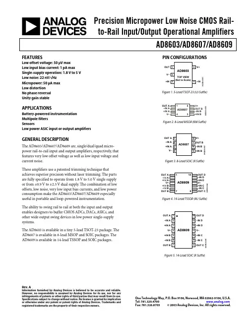
AD8603/AD8607/AD8609
TABLE OF CONTENTS
Specifications..................................................................................... 3 Absolute Maximum Ratings............................................................ 5 Typical Performance Characteristics ............................................. 6 Applications..................................................................................... 12
AD8610ARZ-REEL资料
REV.DInformation furnished by Analog Devices is believed to be accurate and reliable. However, no responsibility is assumed by Analog Devices for itsuse, nor for any infringements of patents or other rights of third parties that may result from its use. No license is granted by implication or otherwise under any patent or patent rights of Analog Devices. Trademarks and registered trademarks are the property of their respective owners.One Technology Way, P.O. Box 9106, Norwood, MA 02062-9106, U.S.A. Tel: 781/329-4700 Fax: 781/326-8703© 2004 Analog Devices, Inc. All rights reserved.AD8610/AD8620 Precision, Very Low Noise,Low Input Bias Current, Wide BandwidthJFET Operational AmplifierFUNCTIONAL BLOCK DIAGRAMS8-Lead MSOP and SOIC(RM-8 and R-8 Suffixes)؊؉VV؉OUTNULLNCNC = NO CONNECT8-Lead SOIC(R-8 Suffix)؊؉V INB INB ؉FEATURESLow Noise 6 nV/√HzLow Offset Voltage: 100 V MaxLow Input Bias Current 10 pA Max Fast Settling: 600 ns to 0.01%Low DistortionUnity Gain StableNo Phase ReversalDual-Supply Operation: ؎5 V to ؎13 V APPLICATIONSPhotodiode AmplifierATEInstrumentationSensors and ControlsHigh Performance FiltersFast Precision IntegratorsHigh Performance AudioGENERAL DESCRIPTIONThe AD8610/AD8620 is a very high precision JFET input amplifier featuring ultralow offset voltage and drift, very low input voltage and current noise, very low input bias current, and wide bandwidth. Unlike many JFET amplifiers, the AD8610/AD8620 input bias current is low over the entire operating temperature range. The AD8610/AD8620 is stable with capacitive loads of over 1000 pF in noninverting unity gain; much larger capacitive loads can be driven easily at higher noise gains. The AD8610/AD8620 swings to within 1.2 V of the supplies even with a 1 kΩ load, maximizing dynamic range even with limited supply voltages. Outputs slew at 50 V/µs in either inverting or noninverting gain configurations, and settle to 0.01% accuracy in less than 600 ns. Combined with the high input impedance, great precision, and very high output drive, the AD8610/AD8620 is an ideal amplifier for driving high performance A/D inputs and buffering D/A converter outputs. Applications for the AD8610/AD8620 include electronic instru-ments; ATE amplification, buffering, and integrator circuits; CAT/MRI/ultrasound medical instrumentation; instrumentation quality photodiode amplification; fast precision filters (including PLL filters); and high quality audio.The AD8610/AD8620 is fully specified over the extended industrial (–40°C to +125°C) temperature range. The AD8610 is available in the narrow 8-lead SOIC and the tiny MSOP8 surface-mount packages. The AD8620 is available in the narrow 8-lead SOIC package. MSOP8 packaged devices are available only in tape and reel.元器件交易网AD8610/AD8620–SPECIFICATIONS(@ V S = ؎5.0 V, V CM = 0 V, T A = 25؇C, unless otherwise noted.) Parameter Symbol Conditions Min Typ Max Unit INPUT CHARACTERISTICSOffset Voltage (AD8610B)V OS45100µV–40°C < T A < +125°C80200µV Offset Voltage (AD8620B)V OS45150µV–40°C < T A < +125°C80300µV Offset Voltage (AD8610A/AD8620A)V OS85250µV+25°C < T A < 125°C90350µV–40°C < T A < +125°C150850µV Input Bias Current I B–10+2+10pA–40°C < T A < +85°C–250+130+250pA–40°C < T A < +125°C–2.5+1.5+2.5nA Input Offset Current I OS–10+1+10pA–40°C < T A < +85°C–75+20+75pA–40°C < T A < +125°C–150+40+150pA Input Voltage Range–2+3V Common-Mode Rejection Ratio CMRR V CM = –2.5 V to +1.5 V9095dB Large Signal Voltage Gain A VO R L = 1 kΩ, V O = –3 V to +3 V100180V/mV Offset Voltage Drift (AD8610B)∆V OS/∆T–40°C < T A < +125°C0.51µV/°C Offset Voltage Drift (AD8620B)∆V OS/∆T–40°C < T A < +125°C0.5 1.5µV/°C Offset Voltage Drift (AD8610A/AD8620A)∆V OS/∆T–40°C < T A < +125°C0.8 3.5µV/°C OUTPUT CHARACTERISTICSOutput Voltage High V OH R L = 1 kΩ, –40°C < T A < +125°C 3.84V Output Voltage Low V OL R L = 1 kΩ, –40°C < T A < +125°C–4–3.8V Output Current I OUT V OUT > ±2 V±30mA POWER SUPPLYPower Supply Rejection Ratio PSRR V S = ±5 V to ±13 V100110dB Supply Current/Amplifier I SY V O = 0 V 2.5 3.0mA–40°C < T A < +125°C 3.0 3.5mA DYNAMIC PERFORMANCESlew Rate SR R L = 2 kΩ4050V/µs Gain Bandwidth Product GBP25MHz Settling Time t S A V = +1, 4 V Step, to 0.01%350ns NOISE PERFORMANCEVoltage Noise e n p-p0.1 Hz to 10 Hz 1.8µV p-p Voltage Noise Density e n f = 1 kHz6nV/√Hz Current Noise Density i n f = 1 kHz5fA/√Hz Input Capacitance C INDifferential8pF Common-Mode15pF Channel Separation C Sf = 10 kHz137dBf = 300 kHz120dB Specifications subject to change without notice.–2–REV. DREV. D AD8610/AD8620–3–ELECTRICAL SPECIFICATIONS (@ V S= ؎13 V, VCM = 0 V, T A = 25؇C, unless otherwise noted.)ParameterSymbol Conditions Min Typ Max Unit INPUT CHARACTERISTICS Offset Voltage (AD8610B)V OS 45100µV –40°C < T A < +125°C 80200µV Offset Voltage (AD8620B)V OS 45150µV –40°C < T A < +125°C 80300µV Offset Voltage (AD8610A/AD8620A)V OS 85250µV +25°C < T A < 125°C 90350µV –40°C < T A < +125°C 150850µV Input Bias Current I B –10+3+10pA –40°C < T A < +85°C –250+130+250pA –40°C < T A < +125°C –3.5+3.5nA Input Offset CurrentI OS–10+1.5+10pA –40°C < T A < +85°C –75+20+75pA –40°C < T A < +125°C–150+40+150pA Input Voltage Range–10.5+10.5V Common-Mode Rejection Ratio CMRR V CM = –10 V to +10 V90110dB Large Signal Voltage GainA VOR L = 1 k Ω, V O = –10 V to +10 V 100200V/mV Offset Voltage Drift (AD8610B)∆V OS /∆T –40°C < T A < +125°C 0.51µV/°C Offset Voltage Drift (AD8620B)∆V OS /∆T –40°C < T A < +125°C 0.5 1.5µV/°C Offset Voltage Drift (AD8610A/AD8620A)∆V OS /∆T –40°C < T A < +125°C0.83.5µV/°COUTPUT CHARACTERISTICS Output Voltage High V OH R L = 1 k Ω, –40°C < T A < +125°C +11.75+11.84VOutput Voltage Low V OL R L = 1 k Ω, –40°C < T A < +125°C –11.84–11.75V Output CurrentI OUT V OUT > 10 V±45mA Short Circuit Current I SC ±65mA POWER SUPPLYPower Supply Rejection Ratio PSRR V S = ±5 V to ±13 V 100110dB Supply Current/Amplifier I SYV O = 0 V3.0 3.5mA –40°C < T A < +125°C 3.54.0mA DYNAMIC PERFORMANCE Slew RateSR R L = 2 k Ω4060V/µs Gain Bandwidth Product GBP 25MHz Settling Timet S A V = 1, 10 V Step, to 0.01%600ns NOISE PERFORMANCE Voltage Noisee n p-p 0.1 Hz to 10 Hz 1.8µV p-p Voltage Noise Density e nf = 1 kHz 6nV/√Hz Current Noise Density i n f = 1 kHz5fA/√Hz Input Capacitance C IN Differential 8pF Common-Mode 15pF Channel Separation C Sf = 10 kHz 137dB f = 300 kHz120dBSpecifications subject to change without notice.REV. D–4–AD8610/AD8620ORDERING GUIDETemperature Package Package ModelRangeDescription Option BrandingAD8610AR–40°C to +125°C 8-Lead SOIC RN-8AD8610AR-REEL –40°C to +125°C 8-Lead SOIC RN-8AD8610AR-REEL7–40°C to +125°C 8-Lead SOIC RN-8AD8610ARM-REEL –40°C to +125°C 8-Lead MSOP RM-8B0A AD8610ARM-R2–40°C to +125°C 8-Lead MSOP RM-8B0AAD8610ARZ *–40°C to +125°C 8-Lead SOIC RN-8AD8610ARZ-REEL *–40°C to +125°C 8-Lead SOIC RN-8AD8610ARZ-REEL7*–40°C to +125°C 8-Lead SOIC RN-8AD8610BR–40°C to +125°C 8-Lead SOIC RN-8AD8610BR-REEL –40°C to +125°C 8-Lead SOIC RN-8AD8610BR-REEL7–40°C to +125°C 8-Lead SOIC RN-8AD8610BRZ *–40°C to +125°C 8-Lead SOIC RN-8AD8610BRZ-REEL *–40°C to +125°C 8-Lead SOIC RN-8AD8610BRZ-REEL7*–40°C to +125°C 8-Lead SOIC RN-8AD8620AR–40°C to +125°C 8-Lead SOIC RN-8AD8620AR-REEL –40°C to +125°C 8-Lead SOIC RN-8AD8620AR-REEL7–40°C to +125°C 8-Lead SOIC RN-8AD8620BR–40°C to +125°C 8-Lead SOIC RN-8AD8620BR-REEL –40°C to +125°C 8-Lead SOIC RN-8AD8620BR-REEL7–40°C to +125°C8-Lead SOICRN-8*Pb-free partABSOLUTE MAXIMUM RATINGS *Supply Voltage . . . . . . . . . . . . . . . . . . . . . . . . . . . . . . . . 27.3 V Input Voltage . . . . . . . . . . . . . . . . . . . . . . . . . . . . . V S–– to V S+Differential Input Voltage . . . . . . . . . . . . . . .± Supply Voltage Output Short-Circuit Duration to GND . . . . . . . . . .Indefinite Storage Temperature RangeR, RM Packages . . . . . . . . . . . . . . . . . . . . .–65°C to +150°C Operating Temperature RangeAD8610/AD8620 . . . . . . . . . . . . . . . . . . . .–40°C to +125°C Junction Temperature RangeR, RM Packages . . . . . . . . . . . . . . . . . . . . .–65°C to +150°C Lead Temperature Range (Soldering, 10 sec) . . . . . . . . 300°C*Stresses above those listed under Absolute Maximum Ratings may cause permanent damage to the device. This is a stress rating only; functional operation of the device at these or any other conditions above those listed in the operational sections of this specification is not implied. Exposure to absolute maximum rating conditions for extended periods may affect device reliability.Package Type JA *JC Unit 8-Lead MSOP (RM)19044°C/W 8-Lead SOIC (RN)15843°C/W*θJA is specified for worst-case conditions; i.e., θJA is specified for a device soldered in circuit board for surface-mount packages.CAUTIONESD (electrostatic discharge) sensitive device. Electrostatic charges as high as 4000V readily accumulate on the human body and test equipment and can discharge without detection. Although the AD8610/AD8620 features proprietary ESD protection circuitry, permanent damage may occur on devices subjected to high energy electrostatic discharges. Therefore, proper ESD precautions are recommended to avoid performance degradation or loss of functionality.REV. D Typical Performance Characteristics–AD8610/AD8620–5–INPUT OFFSET VOL T AGE – V1486421012N U M B E R O F A MP L I F I E R STPC 1.Input Offset Voltage at ±13 VI N P U T O F F S E T V O L T A G E –V600400–600200–200–400TEMPERATURE – ؇CTPC 4.Input Offset Voltage vs.Temperature at ±5 V (300 Amplifiers)SUPPL Y VOL T AGE – ؎V3.01.502.51.00.52.0013123456789101112S U P P L Y C U R R E N T – m ATPC 7.Supply Current vs.Supply Voltage I N P U TO F F S E T V O L T A G E – V600400؊6002000؊200؊400TEMPERATURE – ؇CTPC 2.Input Offset Voltage vs.Temperature at ±13 V (300 Amplifiers)T C V OS – V/؇C141210864200.20.61.01.41.82.22.6N U M B E R O FA M P L I F I E R S TPC 5.Input Offset Voltage DriftTEMPERATURE – ؇C2.553.052.852.652.952.75S U P P L Y C U R R E N T – m A؊40TPC 8.Supply Current vs.Temperature at ±13 V INPUT OFFSET VOL T AGE – V148642101201618؊250250؊15050150؊50N U M B E R O F A M P L I F I E R STPC 3.Input Offset Voltage at ±5 VCOMMON-MODE VOL T AGE – V3.63.42.02.82.62.42.23.23.0I N P U T BI A S C U R R E N T –p ATPC 6.Input Bias Current mon-Mode VoltageTEMPERATURE – ؇C2.302.652.602.402.502.552.452.35S U P P L Y C U R R E N T – m A؊40TPC 9.Supply Current vs.Temperature at ±5 VREV. D–6–AD8610/AD8620O U T P U T V O L T A G E T O S U P P L Y R A I L – VRESIST ANCE LOAD – ⍀100M10M 1M 100k 10k 1k10000.20.40.60.81.01.21.41.61.8TPC 10.Output Voltage to Supply Rail vs. Load 12.0511.8012.0011.9511.9011.85O U T P U T V O L T A G E H I G H –VTEMPERA TURE – ؇CTPC 13.Output Voltage High vs. Temperature at ±13 VFREQUENCY – Hz10k100k 1M 1k10M 100MC L O S ED -L O O P G A I N – d B؊40؊20206040TPC 16.Closed-Loop Gain vs.FrequencyTEMPERA TURE – ؇C4.254.203.954.154.104.054.00O U T P U T V O L T A G E H I G H – VTPC 11.Output Voltage High vs.Temperature at ±5 VTEMPERA TURE – ؇C؊11.80؊12.05؊11.85؊11.90؊11.95؊12.00O U T P U T V O L T A G E L O W – VTPC 14.Output Voltage Low vs.Temperature at ±13 VTEMPERA TURE – ؇C260100A V O – V /m V220180140240200160120TPC 17.A VO vs. Temperature at ±13 VTEMPERA TURE – ؇C؊3.95؊4.05؊4.30؊4.10؊4.15؊4.20؊4.25؊4.00O U T P U T V O L T A G E L O W – VTPC 12.Output Voltage Low vs.Temperature at ±5 VG A I N – d B40206080100120؊20؊40؊60؊80FREQUENCY – MHzP H A S E – D e g r e e s90450135180225270؊45؊90؊135؊180TPC 15.Open-Loop Gainand Phase vs. FrequencyTEMPERA TURE – ؇C190100180160140120170150130110A V O – V /m V TPC 18.A VO vs. Temperature at ±5 VREV. D AD8610/AD8620–7–P S R R – d BFREQUENCY – Hz60M10k 100k 1M 10M 1001kTPC 19.PSRR vs. Frequency at ±13 V C M R R – d BFREQUENCY – Hz1060M10k 100k 1M 10M1001k 14010080604020120TPC 22.CMRR vs. Frequency TIME – 1s/DIVP -P V O L T A G E N O I S E – 1V /D I VTPC 25.0.1 Hz to 10 Hz Input VoltageNoise P S R R – d B122121116120119118117TEMPERATURE – ؇CTPC 21.PSRR vs. TemperatureTIME – 4s/DIVV O L T A G E – 300m V /D I VTPC 24.Negative OvervoltageRecoveryFREQUENCY – Hz1k100M10k100k1M 10M Z O U T – ⍀TPC 27.Z OUT vs. FrequencyP S R R – d B–401008060400120–2020160140FREQUENCY – Hz60M10k 100k 1M 10M1001kTPC 20.PSRR vs. Frequency at ±5 VTIME – 4s/DIVV O L T A G E – 300m V /D I V0V0VTPC 23.Positive Overvoltage RecoveryFREQUENCY –Hz1,00010011011M10010k101k100kV O L T A G E N O I S E D E N S I T Y – n V TPC 26.Input Voltage Noise vs.FrequencyREV. D–8–AD8610/AD8620FREQUENCY – HzZ O U T – ⍀1009008070605040302010TPC 28.Z OUT vs. FrequencyCAP ACIT ANCE – pF4035030255201510110k 101001k S M A L L S I G N A L O V E R S H O O T – %TPC 31.Small Signal Overshoot vs.Load CapacitanceTIME – 400ns/DIVV O L T A G E – 5V /D I VTPC 34.+SR at G = +1TEMPERA TURE – ؇CI B –p A30002500025851252000150********TPC 29.Input Bias Current vs.TemperatureTIME – 400s/DIVV O L T A G E – 5V /D I VTPC 32.No Phase ReversalTIME – 400ns/DIVV O L T A G E – 5V /D I VTPC 35.–SR at G = +1CAP ACIT ANCE – pF4035030255201510110k101001kS M A L L S I G N A L O V E R S H O O T – %TPC 30.Small Signal Overshoot vs.Load CapacitanceTIME – 1s/DIVV O L T A G E – 5V /D I VTPC rge Signal Response at G = +1TIME – 1s/DIVV O L T A G E – 5V /D I VTPC rge Signal Response at G = –1REV. DAD8610/AD8620–9–TIME – 400ns/DIVV O L T A G E – 5V /D I VTPC 37.+SR at G = –1TIME – 400ns/DIVV O L T A G E – 5V /D I VTPC 38.–SR at G = –1V IN20V p-pCS(dB) = 20 log (V OUT /10 ؋ V IN )Figure 1.Channel Separation Test CircuitFUNCTIONAL DESCRIPTIONThe AD8610/AD8620 is manufactured on Analog Devices, Inc.’s proprietary XFCB (eXtra Fast Complementary Bipolar) process.XFCB is fully dielectrically isolated (DI) and used in conjunc-tion with N-channel JFET technology and trimmable thin-film resistors to create the world’s most precise JFET input amplifier.Dielectrically isolated NPN and PNP transistors fabricated on XFCB have F T greater than 3 GHz. Low T C thin film resistors enable very accurate offset voltage and offset voltage tempcotrimming. These process breakthroughs allowed Analog Devices’world class IC designers to create an amplifier with faster slew rate and more than 50% higher bandwidth at half of the current consumed by its closest competition. The AD8610 is uncondi-tionally stable in all gains, even with capacitive loads well in excess of 1 nF. The AD8610B achieves less than 100 µV of offset and 1 µV/°C of offset drift, numbers usually associated with very high precision bipolar input amplifiers. The AD8610 is offered in the tiny 8-lead MSOP as well as narrow 8-lead SOIC surface-mount packages and is fully specified with supply voltages from ±5 V to ±13 V. The very wide specified temperature range, up to 125°C, guarantees superior operation in systems with little or no active cooling.The unique input architecture of the AD8610 features extremely low input bias currents and very low input offset voltage. Low power consumption minimizes the die temperature and maintains the very low input bias current. Unlike many competitive JFET amplifiers, the AD8610/AD8620 input bias currents are low even at elevated temperatures. Typical bias currents are less than 200pA at 85°C. The gate current of a JFET doubles every 10°C resulting in a similar increase in input bias current over temperature.Special care should be given to the PC board layout to minimize leakage currents between PCB traces. Improper layout and board handling generates leakage current that exceeds the bias current of the AD8610/AD8620.FREQUENCY – kHz35050100150200250300138136120128126124122132130134C S – d BFigure 2.AD8620 Channel Separation GraphPower ConsumptionA major advantage of the AD8610/AD8620 in new designs is the saving of power. Lower power consumption of the AD8610makes it much more attractive for portable instrumentation and for high-density systems, simplifying thermal management, and reducing power supply performance requirements. Compare the power consumption of the AD8610/AD8620 versus the OPA627in Figure 3.TEMPERA TURE – ؇C8765432S U P P L Y C U R R E N T – m AFigure 3.Supply Current vs. TemperatureREV. D–10–AD8610/AD8620Driving Large Capacitive LoadsThe AD8610 has excellent capacitive load driving capability and can safely drive up to 10 nF when operating with ±5 V supply.Figures 4 and 5 compare the AD8610/AD8620 against the OPA627in the noninverting gain configuration driving a 10 k Ω resistor and 10,000 pF capacitor placed in parallel on its output, with a square wave input set to a frequency of 200 kHz. The AD8610 has much less ringing than the OPA627 with heavy capacitive loads.TIME – 2s/DIVV O L T A G E – 20m V /D IVFigure 4.OPA627 Driving C L = 10,000 pFTIME – 2s/DIVV O L T A G E – 20m V /D IVFigure 5.AD8610/AD8620 Driving C L = 10,000 pFThe AD8610/AD8620 can drive much larger capacitances without any external compensation. Although the AD8610/AD8620 is stable with very large capacitive loads, remember that this capacitive loading will limit the bandwidth of the amplifier. Heavy capacitive loads will also increase the amount of overshoot and ringing at the output. Figures 7 and 8 show the AD8610/AD8620 and the OPA627in a noninverting gain of +2 driving 2 µF of capacitance load. The ringing on the OPA627 is much larger in magnitude and continues more than 10 times longer than the AD8610.2FFigure 6.Capacitive Load Drive Test CircuitTIME – 20s/DIVV O L T A G E – 50m V /D I VFigure 7.OPA627 Capacitive Load Drive, A V = +2TIME – 20s/DIVV O L T A G E – 50m V /D I VFigure 8.AD8610/AD8620 Capacitive Load Drive, A V = +2Slew Rate (Unity Gain Inverting vs. Noninverting)Amplifiers generally have a faster slew rate in an inverting unity gain configuration due to the absence of the differential input capacitance. Figures 9 through 12 show the performance of the AD8610 configured in a gain of –1 compared to the OPA627.The AD8610 slew rate is more symmetrical, and both the positive and negative transitions are much cleaner than in the OPA627.REV. D AD8610/AD8620–11–TIME – 400ns/DIVV O L T A G E – 5V /D I VFigure 9.(+SR) of AD8610/AD8620 in Unity Gain of –1TIME – 400ns/DIVV O L T A G E – 5V /D I VFigure 10.(+SR) of OPA627 in Unity Gain of –1TIME – 400ns/DIVV O L T A G E – 5V /D I VFigure 11.(–SR) of AD8610/AD8620 in Unity Gain of –1TIME – 400ns/DIVV O L T A G E – 5V /D IVFigure 12.(–SR) of OPA627 in Unity Gain of –1The AD8610 has a very fast slew rate of 60 V/µs even when config-ured in a noninverting gain of +1. This is the toughest condition to impose on any amplifier since the input common-mode capacitance of the amplifier generally makes its SR appear worse. The slew rate of an amplifier varies according to the voltage difference between its two inputs. To observe the maximum SR as specified in the AD8610 data sheet, a difference voltage of about 2 V between the inputs must be ensured. This will be required for virtually any JFET op amp so that one side of the op amp input circuit is com-pletely off, maximizing the current available to charge and discharge the internal compensation capacitance. Lower differential drive voltages will produce lower slew rate readings. A JFET-input op amp with a slew rate of 60 V/µs at unity gain with V IN = 10 V might slew at 20 V/µs if it is operated at a gain of +100 with V IN = 100mV.The slew rate of the AD8610/AD8620 is double that of the OPA627when configured in a unity gain of +1 (see Figures 13 and 14).TIME – 400ns/DIVV O L T A G E – 5V /D I VFigure 13.(+SR) of AD8610/AD8620 in Unity Gain of +1REV. D–12–AD8610/AD8620diodes greatly interfere with many application circuits such as precision rectifiers and comparators. The AD8610 is free from these limitations.+13V 14VFigure 16.Unity Gain FollowerNo Phase ReversalMany amplifiers misbehave when one or both of the inputs are forced beyond the input common-mode voltage range. Phase reversal is typified by the transfer function of the amplifier,effectively reversing its transfer polarity. In some cases, this can cause lockup and even equipment damage in servo systems, and may cause permanent damage or nonrecoverable parameter shifts to the amplifier itself. Many amplifiers feature compensation circuitry to combat these effects, but some are only effective for the inverting input. The AD8610/AD8620 is designed to prevent phase reversal when one or both inputs are forced beyond their input common-mode voltage range.TIME – 400s/DIVV O L T A G E– 5V /D I VFigure 17.No Phase ReversalTHD Readings vs. Common-Mode VoltageTotal harmonic distortion of the AD8610/AD8620 is well below 0.0006% with any load down to 600 Ω. The AD8610/AD8620outperforms the OPA627 for distortion, especially at frequen-cies above 20 kHz.FREQUENCY – HzT H D +N – %Figure 18.AD8610 vs. OPA627 THD + Noise @ V CM= 0 VTIME – 400ns/DIVV O L T A G E – 5V /D I VFigure 14.(+SR) of OPA627 in Unity Gain of +1The slew rate of an amplifier determines the maximum frequency at which it can respond to a large signal input. This frequency (known as full-power bandwidth, or FPBW) can be calculated from the equation:FPBW SRV PEAK =×()2πfor a given distortion (e.g., 1%).V O L T A G E – 10V /D I VTIME – 400ns/DIVFigure 15.AD8610 FPBWInput Overvoltage ProtectionWhen the input of an amplifier is driven below V EE or above V CC by more than one V BE , large currents will flow from the substrate through the negative supply (V–) or the positive supply (V+),respectively, to the input pins, which can destroy the device. If the input source can deliver larger currents than the maximum forward current of the diode (>5 mA), a series resistor can be added to protect the inputs. With its very low input bias and offset current, a large series resistor can be placed in front of the AD8610 inputs to limit current to below damaging levels. Series resistance of 10 k Ωwill generate less than 25 µV of offset. This 10 k Ω will allow input voltages more than 5 V beyond either power supply. Thermal noise generated by the resistor will add 7.5 nV/√Hz to the noise of the AD8610. For the AD8610/AD8620, differential voltages equal to the supply voltage will not cause any problem (see Figure 15).In this context, it should also be noted that the high breakdown voltage of the input FETs eliminates the need to include clamp diodes between the inputs of the amplifier, a practice that is mandatory on many precision op amps. Unfortunately, clampREV. D AD8610/AD8620–13–FREQUENCY – HzT H D + N – %Figure 19.THD + Noise vs. FrequencyNoise vs. Common-Mode VoltageAD8610 noise density varies only 10% over the input range as shown in Table I.Table I.Noise vs. Common-Mode VoltageV CM at F = 1 kHz (V)Noise Reading (nV/√Hz )–107.21–5 6.890 6.73+5 6.41+107.21Settling TimeThe AD8610 has a very fast settling time, even to a very tight error band, as can be seen from Figure 20. The AD8610 is configured in an inverting gain of +1 with 2 k Ω input and feedback resistors.The output is monitored with a 10×, 10 M, 11.2 pF scope probe.ERROR BAND – %1.2k0.001100.01S E T T L I N G T I M E – n s0.118004001.0k600200Figure 20.AD8610 Settling Time vs. Error BandERROR BAND – %1.2k1.0k 0S E T T L I N G T I M E – n s800600200400Figure 21.OPA627 Settling Time vs. Error BandThe AD8610/AD8620 maintains this fast settling when loaded with large capacitive loads as shown in Figure 22.C L – pF02000500S E T T L I N G T I M E – s100015003.02.00.01.02.51.50.5Figure 22.AD8610 Settling Time vs. Load CapacitanceC L – pF02000500S E T T L I N G T I M E – s10001500Figure 23.OPA627 Settling Time vs. Load Capacitance Output Current CapabilityThe AD8610 can drive very heavy loads due to its high output current. It is capable of sourcing or sinking 45 mA at ±10 V output.The short circuit current is quite high and the part is capable of sinking about 95 mA and sourcing over 60 mA while operating withREV. D–14–AD8610/AD8620supplies of ±5 V. Figures 24 and 25 compare the load current versus output voltage of AD8610/AD8620 and OPA627.LOAD CURRENT – A100.10.000011D E L T A F R O M R E S P E C T I V E R A I L – V10.00010.0010.010.1Figure 24.AD8610 Dropout from ±13 V vs. Load CurrentLOAD CURRENT – A100.10.000011D E L T A F R O M R E S P E C T I V E R A I L – V10.00010.0010.010.1Figure 25.OPA627 Dropout from ±15 V vs. Load CurrentAlthough operating conditions imposed on the AD8610 (±13 V)are less favorable than the OPA627 (±15 V), it can be seen that the AD8610 has much better drive capability (lower headroom to the supply) for a given load current.Operating with Supplies Greater than ±13 VThe AD8610 maximum operating voltage is specified at ±13 V.When ±13 V is not readily available, an inexpensive LDO can provide ±12 V from a nominal ±15 V supply.Input Offset Voltage AdjustmentOffset of AD8610 is very small and normally does not require additional offset adjustment. However, the offset adjust pins can be used as shown in Figure 26 to further reduce the dc offset. By using resistors in the range of 50 k Ω, offset trim range is ±3.3 mV.+V OUTSFigure 26.Offset Voltage Nulling CircuitProgrammable Gain Amplifier (PGA)The combination of low noise, low input bias current, low input offset voltage, and low temperature drift make the AD8610 a perfect solution for programmable gain amplifiers. PGAs are often used immediately after sensors to increase the dynamic range of the measurement circuit. Historically, the large ON resistance of switches, combined with the large I B currents of amplifiers,created a large dc offset in PGAs. Recent and improved monolithic switches and amplifiers completely remove these problems. A PGA discrete circuit is shown in Figure 27. In Figure 27, when the 10 pA bias current of the AD8610 is dropped across the (<5 Ω) R ON of the switch, it results in a negligible offset error.When high precision resistors are used, as in the circuit of Figure 27,the error introduced by the PGA is within the 1/2 LSB requirement for a 16-bit system.Figure 27.High Precision PGA1. Room temperature error calculation due to R ON and I B :∆Ω∆∆V I R Total Offset Offset V Total Offset Offset Trimmed V Total Offset OS B ON OSOS =×=×==+=+=+≅25105105pA pV () (_) V pV V AD8610AD8610µµ2. Full temperature error calculation due to R ON and I B :∆ΩV I R OS B ON (C)(C)(C)pA .nV @@@85858525015375°=°×°=×=3. Temperature coefficient of switch and AD8610/AD8620combined is essentially the same as the T C V OS of the AD8610: ∆∆∆∆∆∆∆∆V T total V T V T I R V T total OS OS OS B ON OS /()/()/()/().V/C .nV/C .V/C =+×=°+°≅°AD86100500605µµ。
AD8326ARP-REEL资料
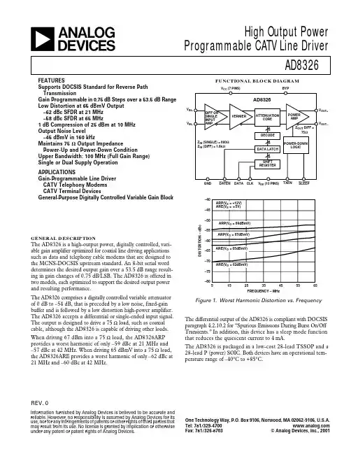
High Output Power Programmable CATV Line Driver AD8326
FUNCTIONAL BLOCK DIAGRAM
VCC (7 PINS) BYP
AD8326
VIN+ DIFF OR SINGLE INPUT AMP VOUT+ VERNIER
ATTENUATION CORE
1 dB Compression Point Differential Output Impedance OVERALL PERFORMANCE Worst Harmonic Distortion
Max Gain, f = 10 MHz Transmit Enable and Transmit Disable Mode f = 14 MHz, VOUT = 67 dBmV @ Max Gain f = 21 MHz, VOUT = 67 dBmV @ Max Gain f = 42 MHz, VOUT = 67 dBmV @ Max Gain f = 65 MHz, VOUT = 67 dBmV @ Max Gain 16 QAM, VOUT = 67 dBmV Adj Ch Wid = Tr Ch Wid = 160 KSYM/SEC Min to Max Gain Max Gain, VIN = 0 V to 0.25 V p-p Min Gain, TXEN = 0, 65 MHz, V IN = 0.25 V p-p Max Gain, TXEN = 0, 42 MHz, V IN = 0.25 V p-p Max Gain, TXEN = 0, 65 MHz, V IN = 0.25 V p-p All Gains, SLEEP, 65 MHz, V IN = 0.25 V p-p
AD648KR-REEL7中文资料
Information furnished by Analog Devices is believed to be accurate and reliable. However, no responsibility is assumed by Analog Devices for its use, nor for any infringements of patents or other rights of third parties which may result from its use. No license is granted by implication or otherwise under any patent or patent rights of Analog Devices.
AD9661AKR-REEL资料
VREF –50 25 0.1 –10 130 –32 0.95 120 2.50 2 1.0
VREF + 1.6 +50 1.6 0 +32 1.05
V µA MHz V µA MHz mV V/V mA V mA µA MHz ns ns ns ns ns ns nA V pF V V V V µA mA V mV/°C mA mA/mA V Ω V mA
CHOLD = 33 pF, RF = 1 kΩ, CF = 2 pF
VOUT = 2.5 V PULSE = LOW, DISABLE = LOW PULSE = LOW, DISABLE = HIGH Output Current –3 dB
5.25 5.0 1.0
2.9 3.2
200 3.9 3.7 1.5 1.5 13 3
LASER DIODE
OUTPUT
8
AD9661A
ANALOG POWER MONITOR VREF
IMONITOR
1:1
SENSE IN IMONITOR 1.0V
REV. 0
Information furnished by Analog Devices is believed to be accurate and reliable. However, no responsibility is assumed by Analog Devices for its use, nor for any infringements of patents or other rights of third parties which may result from its use. No license is granted by implication or otherwise under any patent or patent rights of Analog Devices. © Analog Devices, Inc., 1995 One Technology Way, P.O. Box 9106, Norwood, MA 02062-9106, U.S.A. Tel: 617/329-4700 Fax: 617/326-8703
AD7874ARZ-REEL中文资料
One Technology Way, P.O. Box 9106, Norwood, M329-4700 Fax: 617/326-8703
元器件交易网
AD7874–SPECIFICATIONS external. All specifications T
Parameter SAMPLE-AND-HOLD Acquisition Time2 to 0.01% Droop Rate2, 3 –3 dB Small Signal Bandwidth3 Aperture Delay2 Aperture Jitter2, 3 Aperture Delay Matching2 SAMPLE-AND-HOLD AND ADC DYNAMIC PERFORMANCE Signal-to-Noise Ratio Total Harmonic Distortion Peak Harmonic or Spurious Noise Intermodulation Distortion 2nd Order Terms 3rd Order Terms Channel-to-Channel Isolation2 DC ACCURACY Resolution Relative Accuracy Differential Nonlinearity Positive Full-Scale Error4 Negative Full-Scale Error4 Full-Scale Error Match Bipolar Zero Error Bipolar Zero Error Match ANALOG INPUTS Input Voltage Range Input Current REFERENCE OUTPUTS REF OUT REF OUT Error @ +25°C TMIN to TMAX REF OUT Temperature Coefficient Reference Load Change REFERENCE INPUT Input Voltage Range Input Current Input Capacitance3 LOGIC INPUTS Input High Voltage, VINH Input Low Voltage, VINL Input Current, IIN Input Capacitance, CIN3 LOGIC OUTPUTS Output High Voltage, VOH Output Low Voltage, VOL DB0–DB11 Floating-State Leakage Current Floating-State Output Capacitance Output Coding POWER REQUIREMENTS VDD VSS IDD ISS Power Dissipation A Version B Version S Version Units 2 1 500 0 40 200 4 2 1 500 0 40 200 4 2 2 500 0 40 200 4 µs max mV/ms max kHz typ ns min ns max ps typ ns max
AD7417ARU-REEL中文资料
REV.GAD7416/AD7417/AD7418 10-Bit Digital Temperature Sensor (AD7416) and Four Single-Channel ADCs (AD7417/AD7418)Information furnished by Analog Devices is believed to be accurate and reliable. However, no responsibility is assumed by Analog Devices for itsuse, nor for any infringements of patents or other rights of third parties that may result from its use. No license is granted by implication or otherwise under any patent or patent rights of Analog Devices. Trademarks and registered trademarks are the property of their respective owners.One Technology Way, P.O. Box 9106, Norwood, MA 02062-9106, U.S.A. Tel: 781/329-4700 Fax: 781/326-8703© 2004 Analog Devices, Inc. All rights reserved.FEATURES10-Bit ADC with 15 s and 30 s Conversion Times Single and Four Single-Ended Analog Input Channels On-Chip Temperature Sensor: –40؇C to +125؇COn-Chip Track-and-HoldOvertemperature IndicatorAutomatic Power-Down at the End of a Conversion Wide Operating Supply Range: 2.7 V to 5.5 VI2C® Compatible Serial InterfaceSelectable Serial Bus Address Allows Connection of up to Eight AD7416/AD7417s to a Single BusAD7416 Is a Superior Replacement for LM75 APPLICATIONSData Acquisition with Ambient Temperature Monitoring Industrial Process ControlAutomotiveBattery-Charging ApplicationsPersonal ComputersFUNCTIONAL BLOCK DIAGRAMSV DDOTIA0A1A2VOTISCLSDAA2A1A0CONVSTA IN1A IN2A IN3A IN4NC NC GNDNC = NO CONNECTVSCLSDA A IN1REFCONVSTGENERAL DESCRIPTIONThe AD7417 and AD7418 are 10-bit, 4-channel and single-channel ADCs with an on-chip temperature sensor that can operate from a single 2.7 V to 5.5 V power supply. The devices contain a 15 µs successive approximation converter, a 5-channel multiplexer, a temperature sensor, a clock oscilla-tor, a track-and-hold, and a reference (2.5 V). The AD7416 is a temperature-monitoring only device in an 8-lead package. The temperature sensor on the parts can be accessed via multi-plexer Channel 0. When Channel 0 is selected and a conversion is initiated, the resulting ADC code at the end of the conversion gives a measurement of the ambient temperature (±1°C @ 25°C). On-chip registers can be programmed with high and low tem-perature limits, and an open-drain overtemperature indicator (OTI) output is provided, which becomes active when a pro-grammed limit is exceeded.A configuration register allows programming of the sense of the OTI output (active high or active low) and its operating mode (comparator or interrupt). A programmable fault queue counter allows the number of out-of-limit measurements that must occur before triggering the OTI output to be set to prevent spurious triggering of the OTI output in noisy environments.(continued on page 7)AD7416/AD7417/AD7418AD7417/AD7418–SPECIFICATIONS(V DD = 2.7 V to 5.5 V, GND = 0 V, REF IN = 2.5 V, unless otherwise noted.) Parameter A Version B Version1Unit Test Conditions/CommentsDC ACCURACY Any Channel.Resolution1010BitsMinimum Resolution for Which NoMissing Codes Are Guaranteed1010BitsRelative Accuracy2±1±1LSB max This Specification Is Typical for V DD of3.6 V to 5.5 V.Differential Nonlinearity2±1±1LSB max This Specification Is Typical for V DD of3.6 V to 5.5 V.Gain Error2±3±3LSB max External Reference.±10±10LSB max Internal Reference.Gain Error Match2±0.6±0.6LSB max AD7417 Only.Offset Error2±4±4LSB maxOffset Error Match±0.7±0.7LSB max AD7417 Only.ANALOG INPUTSInput Voltage Range V REF V REF V max00V minInput Leakage Current3±1±1µA maxInput Capacitance1010pF maxTEMPERATURE SENSOR1Measurement ErrorAmbient Temperature 25°C±2±1°C maxT MIN to T MAX±3±2°C maxTemperature Resolution1/41/4°C/LSBCONVERSION RATETrack-and-Hold Acquisition Time4400400ns max Source Impedance < 10 Ω.Conversion TimeTemperature Sensor3030µs max Typically 27 µs.Channels 1 to 41515µs max Typically 10 µs.REFERENCE INPUT5, 6REF IN Input Voltage Range6 2.625 2.625V max 2.5 V + 5%.2.375 2.375V min 2.5 V – 5%.Input Impedance4040kΩ minInput Capacitance1010pF maxON-CHIP REFERENCE Nominal 2.5 V.Reference Error6±25±25mV maxTemperature Coefficient68080ppm/°C typDIGITAL INPUTSInput High Voltage, V IH V DD× 0.7V DD× 0.7V minInput Low Voltage, V IL V DD× 0.3V DD× 0.3V maxInput Leakage Current11µA maxDIGITAL OUTPUTSOutput Low Voltage, V OL0.40.4V max I OL = 3 mA.Output High Current11µA max V OH = 5 V.POWER REQUIREMENTSV DD 5.5 5.5V max For Specified Performance.2.7 2.7V minI DD Logic Inputs = 0 V or V DD.Normal Operation600600µA maxPower-Down11µA max50 nA Typically.Auto Power-Down Mode V DD = 3 V. See Operating Modes.10 SPS Throughput Rate66µW typ1 kSPS Throughput Rate6060µW typ10 kSPS Throughput Rate600600µW typPower-Down33µW max Typically 0.15 µW.–2–REV. GREV. G AD7416/AD7417/AD7418–3–NOTES 1B Version applies to AD7417 only with temperature range of –40°C to +85°C. A Version temperature range is –40°C to +125°C. For V DD = 2.7 V, T A = 85°C max and temperature sensor measurement error = ±3°C.2See Terminology.3Refers to the input current when the part is not converting. Primarily due to reverse leakage current in the ESD protection diodes.4Sample tested during initial release and after any redesign or process change that may affect this parameter.5On-chip reference shuts down when external reference is applied.6The accuracy of the temperature sensor is affected by reference tolerance. The relationship between the two is explained in the Temperature Sensor section.Specifications subject to change without notice.AD7416–SPECIFICATIONS(V DD = 2.7 V to 5.5 V, GND = 0 V, REF IN = 2.5 V, unless otherwise noted.)ParameterMinTypMax Unit Test Conditions/Comments TEMPERATURE SENSOR AND ADC Accuracy±2.0°C T A = –25°C to +100°C (V DD = 3 V min)1±3.0°C T A = –40°C to +125°C (V DD = 3 V min)1Resolution10Bits Temperature Conversion Time 40µs Update Rate, t R 400µs OTI Delay 1 × t R6 × t R ms Depends on Fault Queue Setting Supply Current1.0mA I 2C Active 350600µA I 2C Inactive 0.2 1.5µA Shutdown ModeT OTI Default Temperature 80°C T HYST Default Temperature 75°C DIGITAL INPUTSInput High Voltage, V IH V DD × 0.7V DD + 0.5V Input Low Voltage, V IL –0.3V DD × 0.3V Input High Current, I IH +0.005+1.0µA V IN = 5 V Input Low Current, I IL –0.005–1.0µA V IN = 0 VInput Capacitance, C IN 20pF All Digital Inputs DIGITAL OUTPUTSOutput Low Voltage, V OL 0.4V I OL = 3 mA Output High Current 1µA V OH = 5 VOutput Fall Time, t f250ns C L = 400 pF, I O = 3 mA OS Output Low Voltage, V OL0.8V I OUT = 4 mAAC ELECTRICAL CHARACTERISTICS 2AD7416/AD7417/AD7418Serial Clock Period, t 12.5µs See Figure 1Data In Setup Time to SCL High, t 250ns See Figure 1Data Out Stable after SCL Low, t 30ns See Figure 1SDA Low Setup Time to SCL Low (Start Condition), t 450nsSee Figure 1SDA High Hold Time after SCL High (Stop Condition), t 550ns See Figure 1SDA and SCL Fall Time, t 6300nsSee Figure 1NOTES 1For V DD = 2.7 V to 3 V, T A max = 85°C and accuracy = ±3°C.2Sample tested during initial release and after any redesign or process change that may affect this parameter.Specifications subject to change without notice.SCLSDA DATA INSDADATA OUTFigure 1. Diagram for Serial Bus TimingREV. G–4–AD7416/AD7417/AD7418AD7417 PIN FUNCTION DESCRIPTIONPin No.Mnemonic Description1, 16NC No Connection. Do not connect anything to this pin.2SDA Digital I/O. Serial bus bidirectional data. Push-pull output.3SCL Digital Input. Serial bus clock.4OTIThis is a logic output. The overtemperature indicator (OTI) is set if the result of a conversion on Channel 0 (temperature sensor) is greater than an 8-bit word in the overtemperature register (OTR).The signal is reset at the end of a serial read operation. Open-drain output.5REF INReference Input. An external 2.5 V reference can be connected to the AD7417 at this pin. To enable the on-chip reference, the REFIN pin should be tied to GND. If an external reference is connected to the AD7417, the internal reference will shut down.6GND Ground reference for track-and-hold, comparator and capacitor DAC, and digital circuitry.7–10A IN1 to A IN4Analog Input Channels. The AD7417 has four analog input channels. The input channels are single-ended with respect to GND. The input channels can convert voltage signals in the range 0 V to V REF . A chan-nel is selected by writing to the configuration register of the AD7417. (See Control Byte section.)11A2Digital Input. The highest programmable bit of the serial bus address.12A1Digital Input. The middle programmable bit of the serial bus address.13A0Digital Input. The lowest programmable bit of the serial bus address.14V DD Positive Supply Voltage, 2.7 V to 5.5 V.15CONVSTLogic Input Signal. Convert start signal. The rising edge of this signal fully powers up the part. The power-up time for the part is 4 µs. If the CONVST pulse is greater than 4 µs, the falling edge of CONVST places the track-and-hold mode into hold mode and initiates a conversion. If the pulse is less than 4 µs,an internal timer ensures that the track-and-hold does not go into hold and conversion is not initiated until the power-up time has elapsed. The track-and-hold goes into track mode again at the end of con-version. (See Operating Mode section.)AD7417 PIN CONFIGURATIONSOIC/TSSOPNC SDA SCL OTI REF IN GND A A V DDA IN4A IN3REV. G AD7416/AD7417/AD7418–5–AD7416 PIN FUNCTION DESCRIPTIONPin No.Mnemonic Description1SDA Digital I/O. Serial bus bidirectional data. Push-pull output.2SCL Digital Input. Serial bus clock.3OTIThis is a logic output. The OTI is set if the result of a conversion on Channel 0 (temperature sensor) is greater that an 8-bit word in the OTR. The signal is reset at the end of a serial read operation. Open-drain output.4GND Ground reference for track-and-hold, comparator and capacitor DAC, and digital circuitry.5A2Digital Input. The highest programmable bit of the serial bus address.6A1Digital Input. The middle programmable bit of the serial bus address.7A0Digital Input. The lowest programmable bit of the serial bus address.8V DDPositive Supply Voltage, 2.7 V to 5.5 V.AD7418 PIN FUNCTION DESCRIPTIONPin No.Mnemonic Description1SDA Digital I/O. Serial bus bidirectional data. Push-pull output.2SCL Digital Input. Serial bus clock.3OTIThis is a logic output. The OTI is set if the result of a conversion on Channel 0 (temperature sensor) is greater that an 8-bit word in the OTR. The signal is reset at the end of a serial read operation. Open-drain output.4GND Ground reference for track-and-hold, comparator and capacitor DAC, and digital circuitry.5A INAnalog Input Channel. The input channel is single-ended with respect to GND. The input channel can convert voltage signals in the range 0 V to V REF . The analog input channel is selected by writing to the configuration register of the AD7418 and choosing Channel 4. (See Control Byte section.)6REF INReference Input. An external 2.5 V reference can be connected to the AD7418 at this pin. To enable the on-chip reference, the REF IN pin should be tied to GND. If an external reference is connected to the AD7418, the internal reference will shut down.7V DD Positive Supply Voltage, 2.7 V to 5.5 V.8CONVSTLogic Input Signal. Convert start signal. The rising edge of this signal fully powers up the part. The power-up time for the part is 4 µs. If the CONVST pulse is greater than 4 µs, the falling edge ofCONVST places the track-and-hold mode into hold mode and initiates a conversion. If the pulse is less than 4 µs, an internal timer ensures that the track-and-hold does not go into hold and conversion is not initiated until the power-up time has elapsed. The track-and-hold goes into track mode again at the end of conversion. (See Operating Mode section.)AD7416 PIN CONFIGURATIONSOIC/MSOPV DD A0A2A1AD7418 PIN CONFIGURATIONSOIC/MSOPV DD REF INA INAD7416/AD7417/AD7418ABSOLUTE MAXIMUM RATINGS1(T A = 25°C, unless otherwise noted.)V DD to AGND . . . . . . . . . . . . . . . . . . . . . . . . .–0.3V to +7V V DD to DGND . . . . . . . . . . . . . . . . . . . . . . . . .–0.3V to +7VAnalog Input Voltage to AGNDA IN1 to A IN4 . . . . . . . . . . . . . . . . . . .–0.3 V to V DD + 0.3 V Reference Input Voltage to AGND2 . .–0.3 V to V DD + 0.3VDigital Input Voltage to DGND . . . . .–0.3 V to V DD + 0.3 VDigital Output Voltage to DGND . . . .–0.3 V to V DD + 0.3 V Operating Temperature RangeA Version . . . . . . . . . . . . . . . . . . . . . . . . .–40°C to +125°CB Version . . . . . . . . . . . . . . . . . . . . . . . . . .–40°C to +85°C Storage Temperature Range . . . . . . . . . . . .–65°C to +150°CJunction Temperature . . . . . . . . . . . . . . . . . . . . . . . . . . 150°CTSSOP, Power Dissipation . . . . . . . . . . . . . . . . . . . . 450 mW JA Thermal Impedance . . . . . . . . . . . . . . . . . . . . . 120°C/W Lead Temperature, Soldering . . . . . . . . . . . . . . . . . .260°CVapor Phase (60 sec) . . . . . . . . . . . . . . . . . . . . . . .215°C Infrared (15 sec) . . . . . . . . . . . . . . . . . . . . . . . . . . .220°C 16-Lead SOIC Package, Power Dissipation . . . . . . . . 450 mW JA Thermal Impedance . . . . . . . . . . . . . . . . . . . . . 100°C/W Lead Temperature, SolderingVapor Phase (60 sec) . . . . . . . . . . . . . . . . . . . . . . . 215°CInfrared (15 sec) . . . . . . . . . . . . . . . . . . . . . . . . . . . 220°C 8-Lead SOIC Package, Power Dissipation . . . . . . . . . 450 mW JA Thermal Impedance . . . . . . . . . . . . . . . . . . . . . 157°C/W Lead Temperature, SolderingVapor Phase (60 sec) . . . . . . . . . . . . . . . . . . . . . . . 215°C Infrared (15 sec) . . . . . . . . . . . . . . . . . . . . . . . . . . . 220°C MSOP Package, Power Dissipation . . . . . . . . . . . . . . 450 mW JA Thermal Impedance . . . . . . . . . . . . . . . . . . . . . 206°C/W Lead Temperature, SolderingVapor Phase (60 sec) . . . . . . . . . . . . . . . . . . . . . . . 215°C Infrared (15 sec) . . . . . . . . . . . . . . . . . . . . . . . . . . . 220°C NOTES1Stresses above those listed under Absolute Maximum Ratings may cause perma-nent damage to the device. This is a stress rating only; functional operation of the device at these or any other conditions above those listed in the operational sections of this specification is not implied. Exposure to absolute maximum rating conditions for extended periods may affect device reliability.2If the reference input voltage is likely to exceed VDDby more than 0.3 V (e.g., during power-up) and the reference is capable of supplying 30 mA or more, it is recommended to use a clamping diode between the REF IN pin and V DD pin. The diagram below shows how the diode should be connected.CAUTIONESD (electrostatic discharge) sensitive device. Electrostatic charges as high as 4000V readilyaccumulate on the human body and test equipment and can discharge without detection. Although theAD7416/AD7417/AD7418 features proprietary ESD protection circuitry, permanent damage mayoccur on devices subjected to high energy electrostatic discharges. Therefore, proper ESD precautionsare recommended to avoid performance degradation or loss of functionality.REV. G–6–REV. G AD7416/AD7417/AD7418–7–ORDERING GUIDETemperature Temperature Package Package ModelRangeError DescriptionBrandingOption AD7416ACHIPS DieAD7416AR–40°C to +125°C ±2°C 8-Lead Standard Small Outline Package (SOIC)RN-8AD7416AR-REEL –40°C to +125°C ±2°C 8-Lead Standard Small Outline Package (SOIC)RN-8AD7416AR-REEL7–40°C to +125°C ±2°C 8-Lead Standard Small Outline Package (SOIC)RN-8AD7416ARZ *–40°C to +125°C ±2°C 8-Lead Standard Small Outline Package (SOIC)RN-8AD7416ARZ-REEL *–40°C to +125°C ±2°C 8-Lead Standard Small Outline Package (SOIC)RN-8AD7416ARZ-REEL7*–40°C to +125°C ±2°C 8-Lead Standard Small Outline Package (SOIC)RN-8AD7416ARM–40°C to +125°C ±2°C 8-Lead Micro Small Outline Package (MSOP)C6A RM-8AD7416ARM-REEL –40°C to +125°C ±2°C 8-Lead Micro Small Outline Package (MSOP)C6A RM-8AD7416ARM-REEL7–40°C to +125°C ±2°C 8-Lead Micro Small Outline Package (MSOP)C6A RM-8AD7416ARMZ *–40°C to +125°C ±2°C 8-Lead Micro Small Outline Package (MSOP)C6A RM-8AD7416ARMZ-REEL *–40°C to +125°C ±2°C 8-Lead Micro Small Outline Package (MSOP)C6A RM-8AD7416ARMZ-REEL7*–40°C to +125°C ±2°C 8-Lead Micro Small Outline Package (MSOP)C6ARM-8AD7417ACHIPS DieAD7417AR–40°C to +125°C ±2°C 16-Lead Standard Small Outline Package (SOIC)RN-16AD7417AR-REEL –40°C to +125°C ±2°C 16-Lead Standard Small Outline Package (SOIC)RN-16AD7417AR-REEL7–40°C to +125°C ±2°C 16-Lead Standard Small Outline Package (SOIC)RN-16AD7417ARU–40°C to +125°C ±2°C 16-Lead Thin Shrink Small Outline Package (TSSOP)RU-16AD7417ARU-REEL –40°C to +125°C ±2°C 16-Lead Thin Shrink Small Outline Package (TSSOP)RU-16AD7417ARU-REEL7–40°C to +125°C ±2°C 16-Lead Thin Shrink Small Outline Package (TSSOP)RU-16AD7417BR–40°C to +85°C ±1°C 16-Lead Standard Small Outline Package (SOIC)RN-16AD7417BR-REEL –40°C to +85°C ±1°C 16-Lead Standard Small Outline Package (SOIC)RN-16AD7417BR-REEL7–40°C to +85°C ±1°C 16-Lead Standard Small Outline Package (SOIC)RN-16AD7418ACHIPS DieAD7418AR–40°C to +125°C ±2°C 8-Lead Standard Small Outline Package (SOIC)RN-8AD7418AR-REEL –40°C to +125°C ±2°C 8-Lead Standard Small Outline Package (SOIC)RN-8AD7418AR-REEL7–40°C to +125°C ±2°C 8-Lead Standard Small Outline Package (SOIC)RN-8AD7418ARM–40°C to +125°C ±2°C 8-Lead Micro Small Outline Package (MSOP)C7A RM-8AD7418ARM-REEL –40°C to +125°C ±2°C 8-Lead Micro Small Outline Package (MSOP)C7A RM-8AD7418ARM-REEL7–40°C to +125°C ±2°C 8-Lead Micro Small Outline Package (MSOP)C7ARM-8AD7418ARUZ *–40°C to +125°C ±2°C 16-Lead Thin Shrink Small Outline Package (TSSOP)RU-16AD7418ARUZ-REEL *–40°C to +125°C ±2°C 16-Lead Thin Shrink Small Outline Package (TSSOP)RU-16AD7418ARUZ-REEL7*–40°C to +125°C±2°C16-Lead Thin Shrink Small Outline Package (TSSOP)RU-16EVAL-AD7416/AD7417/Evaluation BoardAD7418EB*Pb-Free PartAD7416/AD7417/AD7418(continued from page 1)An I2C compatible serial interface allows the AD7416/AD7417/ AD7418 registers to be written to and read back. The three LSBs of the AD7416/AD7417’s serial bus address can be selected, which allows up to eight AD7416/AD7417s to be connected to a single bus.The AD7417 is available in a narrow body, 0.15'', 16-lead, small outline IC (SOIC) and in a 16-lead, thin shrink, small outline package (TSSOP). The AD7416 and AD7418 are available in 8-lead SOIC and MSOP packages.PRODUCT HIGHLIGHTS1.The AD7416/AD7417/AD7418 have an on-chip temperaturesensor that allows an accurate measurement of the ambient temperature (±1°C @ 25°C, ±2°C overtemperature) to be made. The measurable temperature range is –40°C to +125°C.An overtemperature indicator is implemented by carrying out a digital comparison of the ADC code for Channel 0 (temperature sensor) with the contents of the on-chip over-temperature register.2.The AD7417 offers a space-saving 10-bit A/D solution withfour external voltage input channels, an on-chip temperature sensor, an on-chip reference, and clock oscillator.3.The automatic power-down feature enables the AD7416/AD7417/AD7418 to achieve superior power performance. At slower throughput rates, the part can be programmed to operate in a low power shutdown mode, allowing further savings in power consumption.TERMINOLOGYRelative AccuracyRelative accuracy or endpoint nonlinearity is the maximum deviation from a straight line passing through the endpoints of the ADC transfer function.Differential NonlinearityThis is the difference between the measured and the ideal 1LSB change between any two adjacent codes in the ADC.Offset ErrorThis is the deviation of the first code transition (0000 . . . 000) to (0000 . . . 001) from the ideal, i.e., GND + 1 LSB.Offset Error MatchThis is the difference in offset error between any two channels. Gain ErrorThis is the deviation of the last code transition (1111 . . . 110) to (1111 . . . 111) from the ideal, i.e., VREF – 1 LSB, after the offset error has been adjusted out.Gain Error MatchThis is the difference in gain error between any two channels. Track-and-Hold Acquisition TimeTrack-and-hold acquisition time is the time required for the output of the track-and-hold amplifier to reach its final value, within ±1/2 LSB, after the end of conversion (the point at which the track-and-hold returns to track mode). It also applies tosituations where a change in the selected input channel takes place or where there is a step input change on the input voltage applied to the selected A IN input of the AD7417 or AD7418. It means that the user must wait for the duration of the track-and-hold acquisition time after the end of conversion or after a channel change/step input change to A IN before starting another conver-sion, to ensure that the part operates to specification.CIRCUIT INFORMATIONThe AD7417 and AD7418 are single-channel and four-channel,15 µs conversion time, 10-bit ADCs with on-chip temperaturesensor, reference, and serial interface logic functions on a single chip. The AD7416 has no analog input channel and is intended for temperature measurement only. The ADC section consists of a conventional successive approximation converter based around a capacitor DAC. The AD7416, AD7417, and AD7418 are capable of running on a 2.7 V to 5.5 V power supply, andthe AD7417 and AD7418 accept an analog input range of 0 V to +VREF. The on-chip temperature sensor allows an accurate measurement of the ambient device temperature to be made.The working measurement range of the temperature sensor is –40°C to +125°C. The parts require a 2.5 V reference that can be provided from the part’s own internal reference or from anexternal reference source.CONVERTER DETAILSConversion is initiated on the AD7417/AD7418 by pulsing the CONVST input. The conversion clock for the part is internally generated so no external clock is required except when reading from and writing to the serial port. The on-chip track-and-hold goes from track to hold mode and the conversion sequence isstarted on the falling edge of the CONVST signal. A conversion is also initiated in the automatic conversion mode every time a read or write operation to the AD7416/AD7417/AD7418 takes place. In this case, the internal clock oscillator (which runs the automatic conversion sequence) is restarted at the end of theread or write operation. The track-and-hold goes into holdapproximately 3 µs after the read or write operation is complete and a conversion is then initiated. The result of the conversion is available either 15 µs or 30 µs later, depending on whether an analog input channel or the temperature sensor is selected. The track-and-hold acquisition time of the AD7417/AD7418 is 400 ns.A temperature measurement is made by selecting the Channel 0of the on-chip mux and carrying out a conversion on this channel.A conversion on Channel 0 takes 30 µs to complete. Tempera-ture measurement is explained in the Temperature Measurement section of this data sheet.The on-chip reference is not available to the user, but REF INcan be overdriven by an external reference source (2.5 V only).All unused analog inputs should be tied to a voltage within the nominal analog input range to avoid noise pickup. For mini-mum power consumption, the unused analog inputs should be tied to GND.REV. G –8–REV. GAD7416/AD7417/AD7418–9–TYPICAL CONNECTION DIAGRAMFigure 2 shows a typical connection diagram for the ing the A0, A1, and A2 pins allows the user to select from up to eight AD7417s on the same serial bus, if desired. An external 2.5 V reference can be connected at the REF IN pin. If an exter-nal reference is used, a 10 µF capacitor should be connected between REF IN and GND. SDA and SCL form the 2-wire I 2C compatible interface. For applications where power consump-tion is of concern, the automatic power-down at the end of a conversion should be used to improve power performance. See Operating Modes section of this data sheet.OPTIONAL EXTERNAL REFERENCEFigure 2. Typical Connection DiagramANALOG INPUTSFigure 3 shows an equivalent circuit of the analog input struc-ture of the AD7417 and AD7418. The two diodes, D1 and D2,provide ESD protection for the analog inputs. Care must be taken to ensure that the analog input signal never exceeds the supply rails by more than 200 mV. This will cause these diodes to become forward-biased and start conducting current into the substrate. The maximum current these diodes can conduct without causing irreversible damage to the part is 20 mA. The capacitor C2 in Figure 3 is typically about 4 pF and can prima-rily be attributed to pin capacitance. The resistor R1 is a lumped component made up of the on resistance of a multiplexer and a switch. This resistor is typically about 1 k Ω. The capacitor C1 is the ADC sampling capacitor and has a capacitance of 3 pF.A BALANCEFigure 3. Equivalent Analog Input CircuitON-CHIP REFERENCEThe AD7416/AD7417/AD7418 has an on-chip 1.2 V band gap reference that is gained up by a switched capacitor amplifier to give an output of 2.5 V. The amplifier is only powered up at the start of the conversion phase and is powered down at the end of the conversion. The on-chip reference is selected by connecting the REF IN pin to analog ground. This causes SW1 (see Figure 4)to open and the reference amplifier to power up during a conver-sion. Therefore, the on-chip reference is not available externally.An external 2.5 V reference can be connected to the REF IN pin.This has the effect of shutting down the on-chip reference circuitry.Figure 4. On-Chip ReferenceTEMPERATURE MEASUREMENTA common method of measuring temperature is to exploit thenegative temperature coefficient of a diode, or the base-emitter voltage of a transistor, operated at a constant current. Unfortu-nately, this technique requires calibration to null out the effect of the absolute value of V BE , which varies from device to device.The technique used in the AD7416/AD7417/AD7418 is to measure the current change in V BE when the device is operated at two different currents.This is given by∆V KT q n N BE =×()/1where:K is Boltzmann ’s constant.q is the charge on the electron (1.6 × 10⁻¹⁹ Coulombs).T is the absolute temperature in Kelvins.N is the ratio of the two currents.OUT ؉OUT ؊Figure 5. Temperature Measurement Technique。
AD8572AR-REEL7资料
Zero-Drift, Single-Supply, Rail-to-RailInput/Output Operational AmplifiersAD8571/AD8572/AD8574 Rev. BInformation furnished by Analog Devices is believed to be accurate and reliable. However, noresponsibility is assumed by Analog Devices for its use, nor for any infringements of patents or other rights of third parties that may result from its use. Specifications subject to change without notice. No license is granted by implication or otherwise under any patent or patent rights of Analog Devices. T rademarks and registered trademarks are the property of their respective owners. O ne Technology Way, P.O. Box 9106, Norwood, MA 02062-9106, U.S.A. Tel: 781.329.4700 Fax: 781.461.3113 ©2006 Analog Devices, Inc. All rights reserved.FEATURESLow offset voltage: 1 μVInput offset drift: 0.005 μV/°CRail-to-rail input and output swing5 V/2.7 V single-supply operationHigh gain, CMRR, PSRR: 130 dBUltralow input bias current: 20 pALow supply current: 750 μA/op ampOverload recovery time: 50 μsNo external capacitors requiredAPPLICATIONSTemperature sensorsPressure sensorsPrecision current sensingStrain gage amplifiersMedical instrumentationThermocouple amplifiersGENERAL DESCRIPTIONThis family of amplifiers has ultralow offset, drift, and bias current. The AD8571, AD8572, and AD8574 are single, dual, and quad amplifiers, respectively, featuring rail-to-rail input and output swings. All are guaranteed to operate from 2.7 V to 5 V single supply.The AD857x family provides benefits previously found only in expensive auto-zeroing or chopper-stabilized amplifiers. Using Analog Devices, Inc. topology, these zero-drift amplifiers combine low cost with high accuracy. (No external capacitors are required.) Using a patented spread-spectrum auto-zero technique, the AD857x family eliminates the intermodulation effects from interaction of the chopping function with the signal frequency in ac applications.With an offset voltage of only 1 μV and drift of 0.005 μV/°C, the AD857x family is perfectly suited for applications where error sources cannot be tolerated. Position and pressure sensors, medical equipment, and strain gage amplifiers benefit greatly from nearly zero drift over their operating temperature range. Many more systems require the rail-to-rail input and output swings provided by the AD857x family.V+OUT ANCNC–IN A+IN AV–NC114-1NC = NO CONNECTNC–IN A+IN AV–114-4Figure 1. 8-Lead MSOP(RM Suffix)Figure 2. 8-Lead SOIC(R Suffix)–IN A+IN AV–OUT B–IN B+IN BOUT A V+114-2–IN A+IN AV–OUT B–IN B+IN BOUT A V+114-5 (RU Suffix)Figure 4. 8-Lead SOIC(R Suffix)OUT A–IN A+IN AV++IN B–IN BOUT B114-3OUT A–IN A+IN AV++IN B–IN BOUT B114-6Figure 5. 14-Lead TSSOP(RU Suffix)Figure 6. 14-Lead SOIC(R Suffix)The AD857x family is specified for the extended industrial/ automotive (−40°C to +125°C) temperature range. The AD8571 single amplifier is available in 8-lead MSOP and narrow 8-lead SOIC packages. The AD8572 dual amplifier is available in8-lead narrow SOIC and 8-lead TSSOP surface mount packages. The AD8574 quad amplifier is available in narrow 14-lead SOIC and 14-lead TSSOP packages.AD8571/AD8572/AD8574Rev. B | Page 2 of 24TABLE OF CONTENTSFeatures..............................................................................................1 Applications.......................................................................................1 General Description.........................................................................1 Pin Configurations...........................................................................1 Revision History...............................................................................2 Specifications.....................................................................................3 5 V Electrical Characteristics......................................................3 2.7 V Electrical Characteristics...................................................4 Absolute Maximum Ratings............................................................5 Thermal Characteristics..............................................................5 ESD Caution..................................................................................5 Typical Performance Characteristics.............................................6 Functional Description..................................................................14 Amplifier Architecture..............................................................14 Basic Auto-Zero Amplifier Theory..........................................14 Auto-Zero Phase.........................................................................14 Amplification Phase...................................................................15 High Gain, CMRR, PSRR..........................................................16 Maximizing Performance T hrough Proper Layout................16 1/f Noise Characteristics...........................................................17 Random Auto-Zero Correction Eliminates Intermodulation Distortion....................................................................................17 Broadband and External Resistor Noise Considerations..........18 Output Overdrive Recovery......................................................18 Input Overvoltage Protection...................................................18 Output Phase Reversal...............................................................18 Capacitive Load Drive...............................................................19 Power-Up Behavior....................................................................19 Applications.....................................................................................20 5 V Precision Strain Gage Circuit............................................20 3 V Instrumentation Amplifier................................................20 High Accuracy Thermocouple Amplifier...............................20 Precision Current Meter............................................................21 Precision Voltage Comparator..................................................21 Outline Dimensions.......................................................................22 Ordering Guide.. (23)REVISION HISTORY09/06—Rev. A to Rev. BUpdated Format..................................................................Universal Renumbered Figures..........................................................Universal Changes to Figure 50......................................................................14 Changes to Figure 51......................................................................15 Changes to Figure 66......................................................................21 Updated Outline Dimensions.......................................................22 Changes to Ordering Guide..........................................................23 07/03—Rev. 0 to Rev. ARenumbered Figures..........................................................Universal Changes to Ordering Guide.............................................................4 Change to Figure 15.......................................................................16 Updated Outline Dimensions. (19)10/99—Revision 0: Initial VersionAD8571/AD8572/AD8574Rev. B | Page 3 of 24SPECIFICATIONS5 V ELECTRICAL CHARACTERISTICSV S = 5 V , V CM = 2.5 V , V O = 2.5 V , T A = 25°C, unless otherwise noted. Table 1.Parameter Symbol Conditions Min Typ Max Unit INPUT CHARACTERISTICS Offset Voltage V OS 1 5 μV −40°C ≤ T A ≤ +125°C 10 μV Input Bias Current I B 10 50 pA −40°C ≤ T A ≤ +125°C 1.0 1.5 nA Input Offset Current I OS 20 70 pA −40°C ≤ T A ≤ +125°C 150 200 pA Input Voltage Range 0 5 V Common-Mode Rejection Ratio CMRR V CM = 0 V to 5 V 120 140 dB −40°C ≤ T A ≤ +125°C 115 130 dBLarge Signal Voltage Gain 1A VO R L = 10 kΩ, V O = 0.3 V to 4.7 V 125 145 dB −40°C ≤ T A ≤ +125°C 120 135 dB Offset Voltage Drift ∆V OS /∆T −40°C ≤ T A ≤ +125°C 0.005 0.04 μV/°C OUTPUT CHARACTERISTICS Output Voltage High V OH R L = 100 kΩ to GND 4.99 4.998 V −40°C to +125°C 4.99 4.997 V R L = 10 kΩ to GND 4.95 4.98 V −40°C to +125°C 4.95 4.975 V Output Voltage Low V OL R L = 100 kΩ to V+ 1 10 mV −40°C to +125°C 2 10 mV R L = 10 kΩ to V+ 10 30 mV −40°C to +125°C 15 30 mV Short-Circuit Limit I SC ±25 ±50 mA −40°C to +125°C ±40 mA Output Current I O ±30 mA −40°C to +125°C ±15 mA POWER SUPPLY Power Supply Rejection Ratio PSRR V S = 2.7 V to 5.5 V 120 130 dB −40°C ≤ T A ≤ +125°C 115 130 dB Supply Current/Amplifier I SY V O = 0 V 850 975 μA −40°C ≤ T A ≤ +125°C 1000 1075 μA DYNAMIC PERFORMANCE Slew Rate SR R L = 10 kΩ 0.4 V/μs Overload Recovery Time 0.05 0.3 ms Gain Bandwidth Product GBP 1.5 MHz NOISE PERFORMANCE Voltage Noise e n p-p 0 Hz to 10 Hz 1.3 μV p-p e n p-p 0 Hz to 1 Hz 0.41 μV p-p Voltage Noise Density e n f = 1 kHz 51 nV/√Hz Current Noise Density i n f = 10 Hz 2 fA/√Hz1Gain testing is dependent upon test bandwidth.AD8571/AD8572/AD8574Rev. B | Page 4 of 242.7 V ELECTRICAL CHARACTERISTICS V S = 2.7 V , V CM = 1.35 V , V O = 1.35 V , T A = 25°C, unless otherwise noted.Table 2.Parameter Symbol Conditions Min Typ Max Unit INPUT CHARACTERISTICS Offset Voltage V OS 1 5 μV −40°C ≤ T A ≤ +125°C 10 μV Input Bias Current I B 10 50 pA −40°C ≤ T A ≤ +125°C 1.0 1.5 nA Input Offset Current I OS 10 50 pA −40°C ≤ T A ≤ +125°C 150 200 pA Input Voltage Range 0 2.7 V Common-Mode Rejection Ratio CMRR V CM = 0 V to 2.7 V 115 130 dB −40°C ≤ T A ≤ +125°C 110 130 dB Large Signal Voltage Gain 1A VO R L = 10 kΩ, V O = 0.3 V to 2.4 V 110 140 dB −40°C ≤ T A ≤ +125°C 105 130 dB Offset Voltage Drift ∆V OS /∆T −40°C ≤ T A ≤ +125°C 0.005 0.04 μV/°C OUTPUT CHARACTERISTICS Output Voltage High V OH R L = 100 kΩ to GND 2.685 2.697 V −40°C to +125°C 2.685 2.696 V R L = 10 kΩ to GND 2.67 2.68 V −40°C to +125°C 2.67 2.675 V Output Voltage Low V OL R L = 100 kΩ to V+ 1 10 mV −40°C to +125°C 2 10 mV R L = 10 kΩ to V+ 10 20 mV −40°C to +125°C 15 20 mV Short-Circuit Limit I SC ±10 ±15 mA −40°C to +125°C ±10 mA Output Current I O ±10 mA −40°C to +125°C ±5 mA POWER SUPPLY Power Supply Rejection Ratio PSRR V S = 2.7 V to 5.5 V 120 130 dB −40°C ≤ T A ≤ +125°C 115 130 dB Supply Current/Amplifier I SY V O = 0 V 750 900 μA −40°C ≤ T A ≤ +125°C 950 1000 μA DYNA MIC PERFOR MANCE Slew Rate SR R L = 10 kΩ 0.5 V/μs Overload Recovery Time 0.05 ms Gain Bandwidth Product GBP 1 MHz NOISE PERFOR MANCE Voltage Noise e n p-p 0 Hz to 10 Hz 2.0 μV p-p Voltage Noise Density e n f = 1 kHz 94 nV/√Hz Current Noise Density i n f = 10 Hz 2 fA/√Hz1Gain testing is dependent upon test bandwidth.AD8571/AD8572/AD8574Rev. B | Page 5 of 24ABSOLUTE MAXIMUM RATINGSTable 3.Parameter RatingSupply Voltage 6 VInput Voltage GND to V S + 0.3 VDifferential Input Voltage 1 ±5.0 VESD (Human Body Model) 2000 VOutput Short-Circuit Duration to GND IndefiniteStorage Temperature RangeRM, RU, and R Packages −65°C to +150°COperating Temperature RangeAD8571A/AD8572A/AD8574A −40°C to +125°CJunction Temperature RangeRM, RU, and R Packages −65°C to +150°C Lead Temperature Range (Soldering, 60 sec) 300°C1Differential input voltage is limited to ±5.0 V or the supply voltage, whichever is less.Stresses above those listed under Absolute Maximum Ratings may cause permanent damage to the device. This is a stress rating only; functional operation of the device at these or any other conditions above those indicated in the operationalsection of this specification is not implied. Exposure to absolute maximum rating conditions for extended periods may affect device reliability.THERMAL CHARACTERISTICSθJA is specified for the worst-case conditions, that is, θJA is specified for a device soldered in a circuit board for SOIC and TSSOP packages. Table 4. Thermal Resistance Package Type θJA θJC Unit 8-Lead MSOP (RM) 190 44 °C/W 8-Lead TSSOP (RU) 240 43 °C/W 8-Lead SOIC (R) 158 43 °C/W 14-Lead TSSOP (RU) 180 36 °C/W 14-Lead SOIC (R) 120 36 °C/W ESD CAUTIONAD8571/AD8572/AD8574Rev. B | Page 6 of 24TYPICAL PERFORMANCE CHARACTERISTICS180012010060204080140160–1.5–2.5–0.50.5 1.5 2.5N U M B E R O F A M P L I F I E R SOFFSET VOLTAGE (µV)01104-007Figure 7. Input Offset Voltage Distribution at 2.7 V50403020100–20–10–30I N P U T B I A S C U R R E N T (p A )INPUT COMMON-MODE VOLTAGE (V)01104-008Figure 8. Input Bias Current vs. Common-Mode Voltage1500–200010005000–1000–1500–500012345I N P U T B I A S C U R R E N T (p A )COMMON-MODE VOLTAGE (V)V S = 5V T A = 125°C01104-009Figure 9. Input Bias Current vs. Common-Mode Voltage 180012010060204080140160N U M B E R O F A M P L I F I E R SOFFSET VOLTAGE (µV)01104-010Figure 10. Input Offset Voltage Distribution at 5 V121086420123465N U M B E R O F A M P L I F I E R SINPUT OFFSET DRIFT (nV/°C)01104-011Figure 11. Input Offset Voltage Drift Distribution at 5 V10k1k1001010.1O U T P U T V O L T A G E (m V )LOAD CURRENT (mA)01104-012Figure 12. Output Voltage to Supply Rail vs. Output Current at 5 VAD8571/AD8572/AD8574Rev. B | Page 7 of 2410k1k 1001010.1O U T P U T V O L T A G E (m V )LOAD CURRENT (mA)01104-013Figure 13. Output Voltage to Supply Rail vs. Output Current at 2.7 V 1000750500250I N P U T B I A S C UR R E N T (p A )TEMPERATURE (°C)01104-014Figure 14. Bias Current vs. Temperature1.00.80.60.40.2S U P P L Y C U R R E N T (m A )TEMPERATURE (°C)01104-015Figure 15. Supply Current vs. Temperature 8002001003004005006007000S U P P L Y C U R R E N T P E R A M P L I F I E R (µA )SUPPLY VOLTAGE (V)01104-016Figure 16. Supply Current vs. Supply Voltage45901351802252700604050102030–100–40–30–20O P E N -L O O P G A I N (d B )P H A S E S H I F T (D e g r e e s )FREQUENCY (Hz)01104-017Figure 17. Open-Loop Gain and Phase Shift vs. Frequency at 2.7 V45901351802252700604050102030–100–40–30–2010k100k 1M10M 100MO P E N -LO O P G A I N (d B )P H A S E S H I F T (D e g r e e s )FREQUENCY (Hz)01104-018Figure 18. Open-Loop Gain and Phase Shift vs. Frequency at 5 VAD8571/AD8572/AD8574Rev. B | Page 8 of 24604050102030–100–40–30–2010010k1k1M100k10MC L O S ED -L O O P G A I N (d B )FREQUENCY (Hz)01104-019Figure 19. Closed-Loop Gain vs. Frequency at 2.7 V 604050102030–100–40–30–20C L O S ED -L O O P G A I N (d B )FREQUENCY (Hz)01104-020Figure 20. Closed-Loop Gain vs. Frequency at 5 V3002402701501802109012003060O U T P U T I M P E D A N C E (Ω)FREQUENCY (Hz)01104-021Figure 21. Output Impedance vs. Frequency at 2.7 V3002402701501802109012003060O U T P U T I M P E D A N C E (Ω)FREQUENCY (Hz)01104-022Figure 22. Output Impedance vs. Frequency at 5 V01104-023Figure 23. Large Signal Transient Response at 2.7 V01104-024Figure 24. Large Signal Transient Response at 5 VAD8571/AD8572/AD8574Rev. B | Page 9 of 2401104-025Figure 25. Small Signal Transient Response at 2.7 V 01104-026Figure 26. Small Signal Transient Response at 5 V101001k10kCAPACITANCE (pF)01104-027S M A L L S I G N A L O V E R S H O O T(%)50450403530252015105Figure 27. Small Signal Overshoot vs. Load Capacitance at 2.7 V450510152025303540S M A L L S I G N A L O V E R S H O O T (%)CAPACITANCE (pF)01104-028Figure 28. Small Signal Overshoot vs. Load Capacitance at 5 V0V V INV OUT0VBOTTOM SCALE: 1V/DIV TOP SCALE: 200mV/DIV01104-029Figure 29. Positive Overvoltage Recovery0VV IN V OUT0VBOTTOM SCALE: 1V/DIV TOP SCALE: 200mV/DIV01104-030Figure 30. Negative Overvoltage RecoveryAD8571/AD8572/AD8574Rev. B | Page 10 of 2401104-031Figure 31. No Phase ReversalC M R R (d B )FREQUENCY (Hz)14080100120600204001104-032Figure 32. CMRR vs. Frequency at 2.7 VC M R R (d B )FREQUENCY (Hz)1408010012060204001104-033Figure 33. CMRR vs. Frequency at 5 VP S R R (d B )FREQUENCY (Hz)14010012001104-034Figure 34. PSRR vs. Frequency at ±1.35 V10010k 1k 10MP S R R (d B )FREQUENCY (Hz)1408010012060204001104-0351M 100kFigure 35. PSRR vs. Frequency at ±2.5 VO U T P U T S W I N G (V p -p )FREQUENCY (Hz)3.01.52.02.51.000.501104-036Figure 36. Maximum Output Swing vs. Frequency at 2.7 VAD8571/AD8572/AD8574Rev. B | Page 11 of 24O U T P U T S W I N G (V p -p )FREQUENCY (Hz)01104-037Figure 37. Maximum Output Swing vs. Frequency at 5 V 0V01104-038Figure 38. 0.1 Hz to 10 Hz Noise at 2.7 V01104-039Figure 39. 0.1 Hz to 10 Hz Noise at 5 V31236420826010415652e n (n V H z )FREQUENCY (kHz)01104-040Figure 40. Voltage Noise Density at 2.7 V from 0 Hz to 2.5 kHz961126480324816e n (n V H z )FREQUENCY (kHz)1104-041Figure 41. Voltage Noise Density at 2.7 V from 0 Hz to 25 kHz156182104130527826e n (n V H z )FREQUENCY (kHz)01104-042Figure 42. Voltage Noise Density at 5 V from 0 Hz to 2.5 kHzAD8571/AD8572/AD8574Rev. B | Page 12 of 24961126480324816e n (n V H z )FREQUENCY (kHz)01104-043Figure 43. Voltage Noise Density at 5 V from 0 Hz to 25 kHz 180210120150609030e n (n V H z )FREQUENCY (kHz)01104-044Figure 44. Voltage Noise Density at 5 V from 0 Hz to 10 Hz150145140130135125P O W E R S U P P L Y R E J E C T I O N (d B )TEMPERATURE (°C)01104-045Figure 45. Power Supply Rejection vs. Temperature50304010–30–10200–40–20–50–75–50–250255075100125150S H OR T -C I R C U I T C U R R E N T (m A )TEMPERATURE (°C)01104-046Figure 46. Output Short-Circuit Current vs. TemperatureAD8571/AD8572/AD8574Rev. B | Page 13 of 24100608020–60–20400–80–40–100–75–50–25255075100125150S H O R T -C I R C U I T C U R R E N T (m A )TEMPERATURE (°C)01104-047Figure 47. Output Short-Circuit Current vs. TemperatureO U T P U T V O L T A G E S W I N G (m V )TEMPERATURE (°C)100250200015025507512517522501104-048Figure 48. Output Voltage to Supply Rail vs. TemperatureO U T P U T V O L T A G E S W I N G (m V )TEMPERATURE (°C)100250200015025507512517522501104-049Figure 49. Output Voltage to Supply Rail vs. TemperatureAD8571/AD8572/AD8574Rev. B | Page 14 of 24FUNCTIONAL DESCRIPTIONThe AD8571/AD8572/AD8574 are CMOS amplifiers that achieve their high degree of precision through randomfrequency auto-zero stabilization. The autocorrection topology allows the AD857x to maintain its low offset voltage over a wide temperature range, and the randomized auto-zero clockeliminates any intermodulation distortion (IMD) errors at the amplifier output.The AD857x can be run from a single-supply voltage as low as 2.7 V . The extremely low offset voltage of 1 μV and no IMD products allows the amplifier to be easily configured for high gains without risk of excessive output voltage errors. This makes the AD857x an ideal amplifier for applications requiring both dc precision and low distortion for ac signals. The extremely small temperature drift of 5 nV/°C ensures a minimum of offset voltage error over its entire temperature range of −40°C to +125°C. These combined features make the AD857x an excellent choice for a variety of sensitive measurement and automotive applications.AMPLIFIER ARCHITECTUREEach AD857x op amp consists of two amplifiers: a main amplifier and a secondary amplifier that is used to correct the offset voltage of the main amplifier. Both consist of a rail-to-rail input stage, allowing the input common-mode voltage range to reach both supply rails. The input stage consists of an NMOS differential pair operating concurrently with a parallel PMOS differential pair. The outputs from the differential input stages are combined in another gain stage whose output is used to drive a rail-to-rail output stage.The wide voltage swing of the amplifier is achieved by using two output transistors in a common-source configuration. The output voltage range is limited by the drain-to-source resistance of these transistors. As the amplifier is required to source or sink more output current, the voltage drop across these transistors increases due to their on resistance (rds). Simply put, the output voltage does not swing as close to the rail under heavy output current conditions as it does with light output current. This is a characteristic of all rail-to-rail output amplifiers. Figure 12 and Figure 13 show how close the output voltage can get to the rails with a given output current. The output of the AD857x is short-circuit protected to approximately 50 mA of current.The AD857x amplifiers have exceptional gain, yielding greater than 120 dB of open-loop gain with a load of 2 kΩ. Because the output transistors are configured in a common-source configura-tion, the gain of the output stage, and thus the open-loop gain of the amplifier, is dependent on the load resistance. Open-loop gain decreases with smaller load resistances. This is another characteristic of rail-to-rail output amplifiers.BASIC AUTO-ZERO AMPLIFIER THEORYAutocorrection amplifiers are not a new technology. Various IC implementations have been available for more than 15 years and some improvements have been made over time. The AD857x design offers a number of significant performance improve-ments over older versions while attaining a very substantial reduction in device cost. This section offers a simplified explanation of how the AD857x is able to offer extremely low offset voltages and high open-loop gains.As noted in the Amplifier Architecture section, each AD857x op amp contains two internal amplifiers. One is used as the primary amplifier, the other as an autocorrection, or nulling, amplifier. Each amplifier has an associated input offset voltage that can be modeled as a dc voltage source in series with the noninverting input. In Figure 50 and Figure 51, these are labeled as V OSX , where X denotes the amplifier associated with the offset: A for the nulling amplifier, B for the primary amplifier. The open-loop gain for the +IN and −IN inputs of each amplifier is given as A X . Both amplifiers also have a third voltage input with an associated open-loop gain of B X . There are two modes of operation determined by the action of two sets of switches in the amplifier: an auto-zero phase and an amplification phase.AUTO-ZERO PHASEIn this phase, all φA switches are closed and all φB switches are opened. Here, the nulling amplifier is taken out of the gain loop by shorting its two inputs together. Of course, there is a degree of offset voltage, shown as V OSA , inherent in the nulling amplifier that maintains a potential difference between the +IN and −IN inputs. The nulling amplifier feedback loop is closed through φA 2 and V OSA appears at the output of the nulling amp and on C M1, an internal capacitor in the AD857x. Mathematically, we can express this in the time domain as][][][t V B t V A t V OA A OSA A OA −= (1)this also can be expressed as[][]AOSA A OA B t V A t V +=1 (2)This shows that the offset voltage of the nulling amplifier times a gain factor appears at the output of the nulling amplifier and thus on the C M1 capacitor.AD8571/AD8572/AD8574Rev. B | Page 15 of 24V IN+V IN–V 01104-050Figure 50. Auto-Zero Phase of the AmplifierAMPLIFICATION PHASEWhen the φB switches close and the φA switches open for the amplification phase, this offset voltage remains on C M1 and essentially corrects any error from the nulling amplifier. The voltage across C M1 is designated as V NA . The potential difference between the two inputs to the primary amplifier is designated as V IN , or V IN = (V IN+ − V IN–). The output of the nulling amplifier can then be expressed as[][][][]t V B t V t V A t V NA A OSA IN A OA −−=( (3)V IN+VIN–V 01104-051Figure 51. Output Phase of the AmplifierBecause φA is now open and there is no place for C M1 to discharge, the voltage (V NA ) at the present time (t) is equal to the voltage at the output of the nulling amp (V OA ) at the time when φA was closed. If the period of the autocorrection switching frequency is designated as T S , then the amplifier switches between phases every 0.5 × T S . Therefore, in the amplification phase[]⎥⎦⎤⎢⎣⎡−=S NA NA T t V t V 21 (4) and substituting Equation 4 and Equation 2 into Equation 3yields[][][]AS OSA A A OSA A IN A OA B T t V B A t V A t V A t V +⎥⎦⎤⎢⎣⎡−−+=121(5) For the sake of simplification, it can be assumed that the autocorrection frequency is much faster than any potential change in V OSA or V OSB . This is a good assumption since changes in offset voltage are a function of temperature variation orlong-term wear time, both of which are much slower than the auto-zero clock frequency of the AD857x. This effectively makes the V OS time invariant, and Equation 5 can be rewritten as[][]()AOSAA A OSA A A IN A OAB V B A V B A t V A t V +−++=11 (6)or[][]⎟⎟⎠⎞⎜⎜⎝⎛++=A OSA IN A OA B V t V A t V 1 (7) Here, the auto-zeroing becomes apparent. Note that the V OSterm is reduced by a 1 + B A factor. This shows how the nulling amplifier has greatly reduced its own offset voltage error even before correcting the primary amplifier. Thus, the primary amplifier output voltage is the voltage at the output of the AD857x amplifier. It is equal to[][]()NB B OSB IN B OUT V B V t V A t V ++= (8)In the amplification phase, V OA = V NB , so this can be rewritten as[][][]⎥⎥⎦⎤⎢⎢⎣⎡⎟⎟⎠⎞⎜⎜⎝⎛++++=A OSA IN A B OSB B IN B OUT B V t V A B V A t V A t V 1 (9) combining terms yields[][]()OSBB AOSAB A B A B IN OUT V A B V B A B A A t V t V ++++=1 (10)The AD857x architecture is optimized in such a way thatA A = AB and B A = B B and B A >> 1. In addition, the gain product to A A B B is much greater than A B . Thus, Equation 10 can be simplified to[][])(OSB OSA A A A IN OUT V V A B A t V t V ++= (11)Most obvious is the gain product of both the primary and nulling amplifiers. This A A B A term is what gives the AD857x its extremely high open-loop gain. To understand how V OSA and V OSB relate to the overall effective input offset voltage of thecomplete amplifier, set up the generic amplifier equation of )(,EFFOS INOUTV V k V +×= (12)where k is the open-loop gain of an amplifier and V OS , EFF is its effective offset voltage. Putting Equation 12 into the form of Equation 11 gives[][]A A EFF OS A A IN OUT B A V B A t V t V ,+= (13) ThereforeAOSBOSA EFF OS B V V V +≈, (14)。
- 1、下载文档前请自行甄别文档内容的完整性,平台不提供额外的编辑、内容补充、找答案等附加服务。
- 2、"仅部分预览"的文档,不可在线预览部分如存在完整性等问题,可反馈申请退款(可完整预览的文档不适用该条件!)。
- 3、如文档侵犯您的权益,请联系客服反馈,我们会尽快为您处理(人工客服工作时间:9:00-18:30)。
Low Cost Micropower, Low Noise CMOS Rail-to-Rail, Input/Output Operational AmplifiersAD8613/AD8617/AD8619 Rev. BInformation furnished by Analog Devices is believed to be accurate and reliable. However, noresponsibility is assumed by Analog Devices for its use, nor for any infringements of patents or other rights of third parties that may result from its use. Specifications subject to change without notice. No license is granted by implication or otherwise under any patent or patent rights of Analog Devices. T rademarks and registered trademarks are the property of their respective owners. O ne Technology Way, P.O. Box 9106, Norwood, MA 02062-9106, U.S.A. Tel: 781.329.4700 Fax: 781.461.3113 ©2006 Analog Devices, Inc. All rights reserved.FEATURESOffset voltage: 2.2 mV maxLow input bias current: 1 pA maxSingle-supply operation: 1.8 V to 5 VLow noise: 22 nV/√HzMicropower: 38 μANo phase reversalUnity gain stableAPPLICATIONSBattery-powered instrumentationMultipole filtersCurrent shunt senseSensorsADC predriversDAC drivers/level shiftersLow power ASIC input or output amplifiersGENERAL DESCRIPTIONThe AD8613/AD8617/AD8619 are single, dual, and quad micropower, rail-to-rail input and output amplifiers that feature low supply current, low input voltage, and low current noise.The parts are fully specified to operate from 1.8 V to 5.0 V single supply, or ±0.9 V and ±2.5 V dual supply. The combination of low noise, very low input bias currents, and low power consumption make the AD8613/AD8617/AD8619 especially useful in portable and loop-powered instrumentation.The ability to swing rail-to-rail at both the input and output enables designers to buffer CMOS ADCs, DACs, ASICs, and other wide output swing devices in low power, single-supply systems.The AD8613 is available in a 5-lead SC70 package and a 5-lead TSOT-23 package. The AD8617 is available in 8-lead MSOP and 8-lead SOIC packages. The AD8619 is available in 14-lead TSSOP and 14-lead SOIC packages.PIN CONFIGURATIONSV+–INOUTV–+IN5622-37 Figure 1. 5-Lead SC70 and 5-Lead TSOT-23 OUT A–IN A+IN AV–V+OUT B–IN B+IN B5622-1Figure 2. 8-Lead MSOP5622-2 OUT A1–IN A2+IN A3V–4V+8OUT B7–IN B6+IN B5AD8617TOP VIEW(Not toScale)Figure 3. 8-Lead SOIC_N5622-35–IN A+IN AV+OUT B–IN B+IN BOUT A–IN D+IN DV–OUT C–IN C+IN COUT DFigure 4. 14-Lead TSSOP5622-36 OUT A–IN A+IN AV+OUT D–IN D+IN DV–+IN B+IN C–IN B–IN COUT B OUT CFigure 5. 14-Lead SOIC_NAD8613/AD8617/AD8619Rev. B | Page 2 of 16TABLE OF CONTENTSFeatures..............................................................................................1 Applications.......................................................................................1 General Description.........................................................................1 Pin Configurations...........................................................................1 Revision History...............................................................................2 Specifications.....................................................................................3 Absolute Maximum Ratings............................................................5 Thermal Resistance.......................................................................5 ESD Caution...................................................................................5 Typical Performance Characteristics..............................................6 Outline Dimensions.......................................................................12 Ordering Guide.. (13)REVISION HISTORY1/06—Rev. A to Rev. BAdded AD8613...................................................................Universal Changes to Features..........................................................................1 Changes to Table 1............................................................................3 Changes to Table 2............................................................................4 Updated Outline Dimensions.......................................................12 Changes to Ordering Guide..........................................................13 10/05—Rev. 0 to Rev. AAdded AD8619...................................................................Universal Change to Specifications Section....................................................3 Updated Outline Dimensions.......................................................12 Changes to Ordering Guide..........................................................13 9/05—Revision 0: Initial VersionAD8613/AD8617/AD8619Rev. B | Page 3 of 16SPECIFICATIONSElectrical characteristics @ V S = 5 V , V CM = V S /2, T A = 25°C, unless otherwise noted. Table 1.Parameter Symbol Conditions Min Typ Max UnitINPUT CHARACTERISTICS Offset Voltage V OS −0.3 V < V CM < +5.3 V0.4 2.2 mV −40°C < T A < +125°C, −0.3 V < V CM < +5.2 V 2.2 mV Offset Voltage Drift ∆V OS /∆T −40°C < T A < +125°C 1 4.5 μV/°C AD8613 2.5 7.0 μV/°C Input Bias Current I B0.2 1 pA −40°C < T A < +85°C110 pA −40°C < T A < +125°C 780 pA Input Offset Current I OS0.1 0.5 pA −40°C < T A < +85°C50 pA −40°C < T A < +125°C 250 pA Common-Mode Rejection Ratio CMRR 0 V < V CM < 5 V95 dB −40°C < T A < +125°C 68 dB Large Signal Voltage Gain A VO R L = 10 kΩ, 0.5 V < V O < 4.5 V 235 500 V/mV Input Capacitance C DIFF 1.9 pF C CM2.5 pF OUTPUT CHARACTERISTICSOutput Voltage High V OH I L = 1 mA 4.95 4.98 V −40°C to +125°C 4.9 V I L = 10 mA 4.7 V −40°C to +125°C 4.50 V Output Voltage Low V OL I L = 1 mA 20 30 mV −40°C to +125°C 50 mV I L = 10 mA 190 275 mV −40°C to +125°C 335 mV Short-Circuit Current I SC ±80 mA Closed-Loop Output Impedance Z OUT f = 10 kHz, A V = 1 15 ΩPOWER SUPPLY Power Supply Rejection Ratio PSRR 1.8 V < V S < 5 V67 94 dB −40°C < T A < +125°C 64 dB Supply Current/Amplifier I SY V O = V S /238 μA −40°C <T A < +125°C 50 μA DYNAMIC PERFORMANCE Slew Rate SR R L = 10 kΩ 0.1 V/μs Settling Time 0.1% t S G = ±1, 2 V step, C L = 20 pF, R L = 1 kΩ 23 μs Gain Bandwidth Product GBP R L = 100 kΩ 400 kHz R L = 10 kΩ 350 kHz Phase Margin ØO R L = 10 kΩ, R L = 100 kΩ, C L = 20 pF 70 Degrees NOISE PERFORMANCE Peak-to-Peak Noise 2.3 3.5 μV Voltage Noise Density e n f = 1 kHz 25 nV/√Hz f = 10 kHz 22 nV/√Hz Current Noise Density i n f = 1 kHz0.05 pA/√HzAD8613/AD8617/AD8619Rev. B | Page 4 of 16Electrical characteristics @ V S = 1.8 V , V CM = V S /2, T A = 25°C, unless otherwise noted. Table 2.Parameter Symbol Conditions Min Typ Max UnitINPUT CHARACTERISTICS Offset Voltage V OS −0.3 V < V CM < +1.9 V 0.4 2.2 mV −0.3 V < V CM < +1.8 V; −40°C < T A < +125°C 2.2 mV Offset Voltage Drift ∆V OS /∆T −40°C < T A < +125°C 1 8.5 μV/°C AD8613 3.7 9.0 μV/°C Input Bias Current I B0.2 1 pA −40°C < T A < +85°C110 pA −40°C < T A < +125°C 780 pA Input Offset Current I OS0.1 0.5 pA −40°C < T A < +85°C50 pA −40°C < T A < +125°C 250 pA Common-Mode Rejection Ratio CMRR 0 V < V CM < 1.8 V58 86 dB −40°C < T A < +125°C 55 dB Large Signal Voltage Gain A VO R L = 10 kΩ, 0.5 V < V O < 1.3 V 85 1000 V/mV Input Capacitance C DIFF 2.1 pF C CM 3.8 pF OUTPUT CHARACTERISTICS Output Voltage High V OH I L = 1 mA 1.65 1.73 V −40°C to +125°C 1.6 V Output Voltage Low V OL I L = 1 mA 44 60 mV −40°C to +125°C 80 mV Short-Circuit Current I SC ±7 mA Closed-Loop Output Impedance Z OUT f = 10 kHz, A V = 115 Ω POWER SUPPLYPower Supply Rejection Ratio PSRR 1.8 V < V S < 5 V 67 94 dB Supply Current/Amplifier I SY V O = V S /238 μA −40°C <T A < +125°C50 μA DYNAMIC PERFORMANCESlew Rate SR R L = 10 kΩ 0.1 V/μs Settling Time 0.1% t S G = ±1, 1 V step, C L = 20 pF, R L = 1 kΩ 6.5 μs Gain Bandwidth Product GBP R L = 100 kΩ 400 kHz R L = 10 kΩ 350 kHz Phase Margin ØO R L = 10 kΩ, R L = 100 kΩ, C L = 20 pF 70 Degrees NOISE PERFORMANCE Peak-to-Peak Noise 2.3 3.5 μV Voltage Noise Density e n f = 1 kHz 25 nV/√Hz f = 10 kHz 22 nV/√Hz Current Noise Density i n f = 1 kHz0.05 pA/√HzAD8613/AD8617/AD8619Rev. B | Page 5 of 16ABSOLUTE MAXIMUM RATINGST A = 25°C, unless otherwise noted . Table 3.Parameter Rating Supply Voltage 6 V Input Voltage V SS − 0.3 V to V DD + 0.3 V Differential Input Voltage ±6 V Output Short-Circuit Duration to GND Observe derating curve Storage Temperature Range −65°C to +150°C Lead Temperature (Soldering, 60 sec) 300°COperating Temperature Range −40°C to +125°CJunction Temperature Range −65°C to +150°CStresses above those listed under Absolute Maximum Ratingsmay cause permanent damage to the device. This is a stress rating only; functional operation of the device at these or any other conditions above those indicated in the operational section of this specification is not implied. Exposure to absolute maximum rating conditions for extended periods may affect device reliability. Absolute maximum ratings apply at 25°C, unless otherwise noted. THERMAL RESISTANCEθJA is specified for the worst-case conditions, that is, a device soldered in a circuit board for surface-mount packages. Table 4. Thermal CharacteristicsPackage TypeθJA θJC Unit 5-Lead TSOT-23 (UJ-5) 207 61 °C/W 5-Lead SC70 (KS-5) 376 126 °C/W 8-Lead MSOP (RM-8) 210 45 °C/W 8-Lead SOIC_N (R-8) 158 43 °C/W 14-Lead SOIC_N (R-14) 120 36 °C/W 14-Lead TSSOP (RU-14)18035 °C/WESD CAUTIONESD (electrostatic discharge) sensitive device. Electrostatic charges as high as 4000 V readily accumulate onthe human body and test equipment and can discharge without detection. Although this product features proprietary ESD protection circuitry, permanent damage may occur on devices subjected to high energy electrostatic discharges. Therefore, proper ESD precautions are recommended to avoid performancedegradation or loss of functionality.AD8613/AD8617/AD8619Rev. B | Page 6 of 16TYPICAL PERFORMANCE CHARACTERISTICSV SY = 5 V or ±2.5 V , unless otherwise noted.1800–2000190005622-003INPUT OFFSET VOLTAGE (μV)N U M B E R O F A M P L I F I E R S1600140012001000800600400200–1700–1400–1100–800–500–20010040070010001300160Figure 6. Input Offset Voltage Distribution40001005622-004TCV OS (μV/°C)N U M B E R O F A M P L I F I E R S3530252015105123456789Figure 7. Input Offset Voltage Drift Distribution 2000–2000–0.55.505622-005INPUT COMMON-MODE VOLTAGE (V)I N P U T O F F S E T V O L T A G E (μV )150010005000–500–1000–150000.5 1.0 1.5 2.0 2.5 3.0 3.5 4.0 4.5 5.0Figure 8. Input Offset Voltage vs. Input Common-Mode Voltage40002515005622-006TEMPERATURE (°C)I N P U T B I A S C U R R E N T (p A)350300250200150100505075100125Figure 9. Input Bias Current vs. Temperature500505622-007SUPPLY VOLT AGE (V)T A = 25°C 403020101234Figure 10. Supply Current vs. Supply Voltage500–4005622-008TEMPERATURE (°C)S U P P L Y C U R R E N T /A M P L I F I E R(μA )40302010–10205080110Figure 11. Supply Current vs. TemperatureAD8613/AD8617/AD8619Rev. B | Page 7 of 161k0.010.0011005622-009LOAD CURRENT (mA)O U T P U T S A T U R A T I O N V O L T A G E (m V )0.010.110.1110100Figure 12. Output Saturation Voltage vs. Load Current 400–4012505622-010TEMPERATURE (°C)O U T P U T S A T U R A T I O N V O L T A G E (m V )302010–25–105203550658095110Figure 13. Output Saturation Voltage vs. Temperature(I L = 1 mA)3500–4012505622-011TEMPERATURE (°C)O U T P U T S A T U R A T I O N V O L T A G E (m V )–25–10520355065809511030025020015010050Figure 14. Output Saturation Voltage vs. Temperature(I L = 10 mA)60–201k1M 05622-012FREQUENCY (Hz)O P E N -L O O P G A I N (d B )–4504590135O P E N -L O O P P H A S E S H I F T (D e g r e e s )10k100k50403020100–10Figure 15. Open-Loop Gain and Phase vs. Frequency12001001M05622-013FREQUENCY (Hz)C M R R (d B )1k 10k10080604020100kFigure 16. CMRR vs. Frequency12001001M05622-014FREQUENCY (Hz)P S R R (d B )1k 10k100k 10080604020Figure 17. PSRR vs. FrequencyAD8613/AD8617/AD8619Rev. B | Page 8 of 161k01001M05622-015FREQUENCY (Hz)O U T P U T I M P E D A N C E (Ω)1k10k100k100101Figure 18. Closed-Loop Output Impedance vs. Frequency50010100005622-016LOAD CAPACITANCE (pF)S M A L L S I G N A L O V E R S H O O T (%)10045403530252015105Figure 19. Small Signal Overshoot vs. Load Capacitance05622-017TIME (4μs/DIV)V O L T A G E (50m V /D I V )Figure 20. Small Signal Transient Response 05622-018TIME (20μs/DIV)V O L T A G E (1V /D I V )Figure 21. Large Signal Transient Response05622-019TIME (20μs/DIV)V O U T (V )V I N (m V )–2.5100Figure 22. Positive Overload Recovery05622-020TIME (20μs/DIV)V O U T (V )V I N (m V )2.5–100Figure 23. Negative Overload RecoveryAD8613/AD8617/AD8619Rev. B | Page 9 of 1605622-021TIME (20μs/DIV)V O L T A G E (1V /D I V )Figure 24. No Phase Reversal 05622-022TIME (1s/DIV)V O L T A G E N O I S E (1μV /D I V)Figure 25. 0.1 Hz to 10 Hz Input Voltage Noise 1000111000005622-023FREQUENCY (Hz)I N P U T V O L T A G E N O I S E (n V /√H z )10100100010100Figure 26. Voltage Noise Density14001001M05622-024FREQUENCY (Hz)C H A N N E L S E P A R A T I O N (d B )204060801001201k 10k100kFigure 27. Channel SeparationAD8613/AD8617/AD8619Rev. B | Page 10 of 16V S = 1.8 V or ±0.9 V , unless otherwise noted.450–2000190005622-025INPUT OFFSET VOLTAGE (μV)N U M B E R O F A M P L I F I E R S40035030025020015010050–1700–1400–1100–800–500–20010040070010001300160Figure 28. Input Offset Voltage Distribution2000–2000–0.5INPUT COMMON-MODE VOLTAGE (V)I N P U T O F F S E T V O L T A G E (μV )2.21500–1500–1000–50005001000–0.20.10.40.7 1.0 1.3 1.6 1.905622-026Figure 29. Input Offset Voltage vs. Input Common-Mode Voltage 10000.010.0011005622-027LOAD CURRENT (mA)O U T P U T S A T U R A T I O N V O L T A G E (m V )0.010.110.1110100Figure 30. Output Saturation Voltage vs. Load Current 800–4012505622-028TEMPERATURE (°C)O U T P U T S A T U R A T I O N V O L T A G E (m V )604020–25–105203550658095110Figure 31. Output Saturation Voltage vs. Temperature(I L = 1 mA)10001001M05622-029FREQUENCY (Hz)C M R R(d B )204060801k 10k100kFigure 32. CMRR vs. Frequency12001001M05622-030FREQUENCY (Hz)P S R R(d B )204060801001k 10kFigure 33. PSRR vs. FrequencyAD8613/AD8617/AD8619400101k05622-031LOAD CAPACITANCE (pF)S M A L L S I G N A L O V E R S H O O T (%)102030100Figure 34. Small Signal Overshoot vs. Load Capacitance05622-032TIME (20μs/DIV)V O L T A G E (500m V /D I V )Figure 35. Large Signal Transient Response 05622-033TIME (1s/DIV)V O L T A G E (1μV /D I V)Figure 36. 0.1 Hz to 10 Hz Input Voltage Noise1k1110k05622-034FREQUENCY (Hz)I N P U T V O L T A G E N O I S E (n V /√H z )101001k 10100Figure 37. Voltage Noise DensityAD8613/AD8617/AD8619OUTLINE DIMENSIONSCOMPLIANT TO JEDEC STANDARDS MO-187-AAPLANE0.10Figure 38. 8-Lead Mini Small Outline Package [MSOP](RM-8)Dimensions shown in millimetersCONTROLLING DIMENSIONS ARE IN MILLIMETERS; INCH DIMENSIONS (IN PARENTHESES) ARE ROUNDED-OFF MILLIMETER EQUIVALENTS FOR REFERENCE ONLY AND ARE NOT APPROPRIATE FOR USE IN DESIGN.COMPLIANT TO JEDEC STANDARDS MS-012-AB45°Figure 39. 14-Lead Standard Small Outline Package [SOIC_N]Narrow Body (R-14)Dimensions shown in millimeters and (inches)CONTROLLING DIMENSIONS ARE IN MILLIMETERS; INCH DIMENSIONS (IN PARENTHESES) ARE ROUNDED-OFF MILLIMETER EQUIVALENTS FOR REFERENCE ONLY AND ARE NOT APPROPRIATE FOR USE IN DESIGN.COMPLIANT TO JEDEC STANDARDS MS-012-AAFigure 40. 8-Lead Standard Small Outline Package [SOIC_N]Narrow Body (R-8)Dimensions shown in millimeters and (inches)PLANE0.10COMPLIANT TO JEDEC STANDARDS MO-153-AB-1Figure 41. 14-Lead Thin Shrink Small Outline Package [TSSOP](RU-14)Dimensions shown in millimetersAD8613/AD8617/AD8619COMPLIANT TO JEDEC STANDARDS MO-203-AA0.460.360.260.10 COPLANARITYFigure 42. 5-Lead Thin Shrink Small Outline Transistor Package [SC70](KS-5)Dimensions shown in millimeters *COMPLIANT TO JEDEC STANDARDS MO-193-AB WITH THE EXCEPTION OF PACKAGE HEIGHT AND THICKNESS.0.50PLANEFigure 43. 5-Lead Thin Small Outline Transistor Package [TSOT-23](UJ-5)Dimensions shown in millimetersORDERING GUIDEModelTemperature Range Package Description Package Option Branding AD8613AKSZ-R21−40°C to +125°C 5-Lead SC70 KS-5 A0Y AD8613AKSZ-REEL 1−40°C to +125°C 5-Lead SC70 KS-5 A0Y AD8613AKSZ-REEL71−40°C to +125°C 5-Lead SC70 KS-5 A0Y AD8613AUJZ-R21−40°C to +125°C 5-Lead TSOT-23 UJ-5 A0Y AD8613AUJZ-REEL 1−40°C to +125°C 5-Lead TSOT-23 UJ-5 A0Y AD8613AUJZ-REEL71−40°C to +125°C 5-Lead TSOT-23 UJ-5 A0Y AD8617ARMZ-R21−40°C to +125°C 8-Lead MSOP RM-8 A0T AD8617ARMZ-REEL 1−40°C to +125°C 8-Lead MSOP RM-8 A0T AD8617ARZ 1−40°C to +125°C 8-Lead SOIC_N R-8 AD8617ARZ-REEL 1−40°C to +125°C 8-Lead SOIC_N R-8 AD8617ARZ-REEL71−40°C to +125°C 8-Lead SOIC_N R-8 AD8619ARUZ 1−40°C to +125°C 14-Lead TSSOP RU-14 AD8619ARUZ-REEL 1−40°C to +125°C 14-Lead TSSOP RU-14 AD8619ARZ 1−40°C to +125°C 14-Lead SOIC_N R-14 AD8619ARZ-REEL 1−40°C to +125°C 14-Lead SOIC_N R-14 AD8619ARZ-REEL71−40°C to +125°C 14-Lead SOIC_N R-141Z = Pb-free part.AD8613/AD8617/AD8619 NOTESAD8613/AD8617/AD8619 NOTESAD8613/AD8617/AD8619 NOTES©2006 Analog Devices, Inc. All rights reserved. Trademarks andregistered trademarks are the property of their respective owners.D05622-0-1/06(B)。