ASB0240中文资料
2SA2004中文资料

Collector-emitter cutoff current (Base open) Forward current transfer ratio
vi
si
VCE = −2V, IC = − 0.1 A VCE = −2 V, IC = −5 V IC = −5 A, IB = − 0.25 A IC = −5 A, IB = − 0.25 A IC = −4 A
at io n.
Max −100 −100 230 −1.2 −1.7 0.5 0.15 1.0
Unit V µA µA V V µs µs µs
Publication date: January 2003
SJD00009CED
1
This product complies with the RoHS Directive (EU 2002/95/EC).
• High forward current transfer ratio hFE • Satisfactory linearity of forward current transfer ratio hFE • Dielectric breakdown voltage of the package: > 5 kV • High−speed switching
at io n.
Request for your special attention and precautions in using the technical information and semiconductors described in this book
(1) If any of the products or technical information described in this book is to be exported or provided to non-residents, the laws and regulations of the exporting country, especially, those with regard to security export control, must be observed. (2) The technical information described in this book is intended only to show the main characteristics and application circuit examples of the products, and no license is granted under any intellectual property right or other right owned by our company or any other company. Therefore, no responsibility is assumed by our company as to the infringement upon any such right owned by any other company which may arise as a result of the use of technical information described in this book. (3) The products described in this book are intended to be used for standard applications or general electronic equipment (such as office equipment, communications equipment, measuring instruments and household appliances). Consult our sales staff in advance for information on the following applications: – Special applications (such as for airplanes, aerospace, automobiles, traffic control equipment, combustion equipment, life support systems and safety devices) in which exceptional quality and reliability are required, or if the failure or malfunction of the products may directly jeopardize life or harm the human body. – Any applications other than the standard applications intended. (4) The products and product specifications described in this book are subject to change without notice for modification and/or improvement. At the final stage of your design, purchasing, or use of the products, therefore, ask for the most up-to-date Product Standards in advance to make sure that the latest specifications satisfy your requirements. (5) When designing your equipment, comply with the range of absolute maximum rating and the guaranteed operating conditions (operating power supply voltage and operating environment etc.). Especially, please be careful not to exceed the range of absolute maximum rating on the transient state, such as power-on, power-off and mode-switching. Otherwise, we will not be liable for any defect which may arise later in your equipment. Even when the products are used within the guaranteed values, take into the consideration of incidence of break down and failure mode, possible to occur to semiconductor products. Measures on the systems such as redundant design, arresting the spread of fire or preventing glitch are recommended in order to prevent physical injury, fire, social damages, for example, by using the products. (6) Comply with the instructions for use in order to prevent breakdown and characteristics change due to external factors (ESD, EOS, thermal stress and mechanical stress) at the time of handling, mounting or at customer's process. When using products for which damp-proof packing is required, satisfy the conditions, such as shelf life and the elapsed time since first opening the packages. (7) This book may be not reprinted or reproduced whether wholly or partially, without the prior written permission of Matsushita Electric Industrial Co., Ltd.
PBSS4480X中文资料

2004 Oct 25
3
Philips Semiconductors
Product specification
80 V, 4 A NPN low VCEsat (BISS) transistor
PBSS4480X
1600 Ptot (mW) 1200
(2) (1)
001aaa229
800
(3)
400
2004 Oct 25
2
Philips Semiconductors
Product specification
80 V, 4 A NPN low VCEsat (BISS) transistor
LIMITING VALUES In accordance with the Absolute Maximum Rating System (IEC 60134). SYMBOL VCBO VCEO VEBO IC ICRM ICM IB IBM Ptot PARAMETER collector-base voltage collector-emitter voltage emitter-base voltage collector current (DC) repetitive peak collector current peak collector current base current (DC) peak base current total power dissipation t ≤ 300 µs Tamb ≤ 25 °C notes 1 and 2 note 2 note 3 note 4 note 5 Tj Tamb Tstg Notes 1. Operated under pulsed conditions; pulse width tp ≤ 10 ms; duty cycle δ ≤ 0.2. junction temperature ambient temperature storage temperature − − − − − − −65 −65 CONDITIONS open emitter open base open collector note 4 tp ≤ 10 ms; δ ≤ 0.1 − − − − − − − MIN.
AOB414资料

SymbolTyp Max 8.1123340R θJL 0.84 1.5Maximum Junction-to-Lead CSteady-State°C/WThermal Characteristics ParameterUnits Maximum Junction-to-Ambient At ≤ 10s R θJA °C/W °C/W Maximum Junction-to-Ambient ASteady-State AOB414, AOB414L ( Green Product )SymbolMin TypMaxUnits BV DSS 30V 1T J =55°C5I GSS 100nA V GS(th)0.8 1.11.5V I D(ON)110A 3.2 4.2T J =125°C563.8 4.8m Ωg FS 102S V SD 0.641V I S110A C iss 9130pF C oss 625pF C rss 387pF R g0.4ΩQ g (4.5V)72.4nC Q gs 12.8nC Q gd 18.4nC t D(on)15ns t r 29.2ns t D(off)106.5ns t f 52ns t rr 31.2ns Q rr20.3nCTHIS PRODUCT HAS BEEN DESIGNED AND QUALIFIED FOR THE CONSUMER MARKET. APPLICATIONS OR USES AS CRITICAL COMPONENTS IN LIFE SUPPORT DEVICES OR SYSTEMS ARE NOT AUTHORIZED. AOS DOES NOT ASSUME ANY LIABILITY ARISING OUT OF SUCH APPLICATIONS OR USES OF ITS PRODUCTS. AOS RESERVES THE RIGHT TO IMPROVE PRODUCT DESIGN,FUNCTIONS AND RELIABILITY WITHOUT NOTICE.Body Diode Reverse Recovery TimeBody Diode Reverse Recovery Charge I F =30A, dI/dt=100A/µsDrain-Source Breakdown Voltage On state drain currentI D =250µA, V GS =0V V GS =4.5V, V DS =5V V GS =10V, I D =30AReverse Transfer Capacitance I F =30A, dI/dt=100A/µsElectrical Characteristics (T J =25°C unless otherwise noted)STATIC PARAMETERS ParameterConditions I DSS µA Gate Threshold Voltage V DS =V GS I D =250µA V DS =24V, V GS =0VV DS =0V, V GS = ±12V Zero Gate Voltage Drain Current Gate-Body leakage current R DS(ON)Static Drain-Source On-ResistanceForward TransconductanceDiode Forward Voltage Maximum Body-Diode Continuous CurrentInput Capacitance Output Capacitance DYNAMIC PARAMETERS m ΩV GS =4.5V, I D =30AI S =1A,V GS =0V V DS =5V, I D =30ATurn-On Rise Time Turn-Off DelayTime V GS =10V, V DS =15V, R L =0.5Ω, R GEN =3ΩTurn-Off Fall TimeTurn-On DelayTime Gate Drain Charge V GS =0V, V DS =15V, f=1MHz SWITCHING PARAMETERS Total Gate Charge Gate Source Charge Gate resistanceV GS =0V, V DS =0V, f=1MHzV GS =4.5V, V DS =15V, I D =30AA: The value of R θJA is measured with the device mounted on 1in 2 FR-4 board with 2oz. Copper, in a still air environment with T A =25°C. The Power dissipation P DSM is based on steady-state R θJA and the maximum allowed junction temperature of 150°C. The value in any a given application depends on the user's specific board design, and the maximum temperature fo 175°C may be used if the PCB or heatsink allows it.B. The power dissipation P D is based on T J(MAX)=175°C, using junction-to-case thermal resistance, and is more useful in setting the upper dissipation limit for cases where additional heatsinking is used. It is used to determine the current rating, when this rating falls below the package limit.C: Repetitive rating, pulse width limited by junction temperature T J(MAX)=175°C.D. The R θJA is the sum of the thermal impedence from junction to case R θJC and case to ambient.E. The static characteristics in Figures 1 to 6 are obtained using <300 µs pulses, duty cycle 0.5% max.F. These tests are performed with the device mounted on 1 in 2FR-4 board with 2oz. Copper, in a still air environment with T A =25°C. The SOA curve provides a single pulse rating.G. The maximum current rating is limited by the package current capability.。
IS42S16400A资料

Integrated Silicon Solution, Inc. — — 1-800-379-47741R e v.C 04/16/03IS42S16400AISSI®Copyright © 2003 Integrated Silicon Solution, Inc. All rights reserved. ISSI reserves the right to make changes to this specification and its products at any time without notice. ISSI assumes no liability arising out of the application or use of any information, products or services described herein. Customers are advised to obtain the latest version of this device specification before relying on any published information and before placing orders for products.FEATURES•Clock frequency:166, 133, 100 MHz•Fully synchronous; all signals referenced to a positive clock edge •Internal bank for hiding row access/precharge •Single 3.3V power supply •LVTTL interface•Programmable burst length – (1, 2, 4, 8, full page)•Programmable burst sequence:Sequential/Interleave •Self refresh modes•4096 refresh cycles every 64 ms•Random column address every clock cycle •Programmable CAS latency (2, 3 clocks)•Burst read/write and burst read/single write operations capability •Burst termination by burst stop and precharge command •Byte controlled by LDQM and UDQM •Industrial temperature availability (133MHz, 100MHz)•Package: 400-mil 54-pin TSOP II,a lead-free package is available.OVERVIEWISSI 's 64Mb Synchronous DRAM IS42S16400A is organizedas 1,048,576 bits x 16-bit x 4-bank for improved performance. The synchronous DRAMs achieve high-speed data transfer using pipeline architecture. All inputs and outputs signals refer to the rising edge of the clock input.1 Meg Bits x 16 Bits x 4 Banks (64-MBIT)SYNCHRONOUS DYNAMIC RAMApril 2003PIN CONFIGURATIONS54-Pin TSOP (Type II)PIN DESCRIPTIONSA0-A11Address Input BA0, BA1Bank Select Address I/O0 to I/O15Data I/OCLK System Clock Input CKE Clock Enable CS Chip SelectRAS Row Address Strobe Command CASColumn Address Strobe CommandWE Write EnableLDQM Lower Bye, Input/Output Mask UDQM Upper Bye, Input/Output Mask Vcc Power GND GroundVcc Q Power Supply for I/O Pin GND Q Ground for I/O Pin NCNo Connection元器件交易网IS42S16400AISSI®2Integrated Silicon Solution, Inc. — — 1-800-379-4774R e v.C 04/16/03GENERAL DESCRIPTIONThe 64Mb SDRAM is a high speed CMOS, dynamic random-access memory designed to operate in 3.3V memory systems containing 67,108,864 bits. Internally configured as a quad-bank DRAM with a synchronous interface. Each 16,777,216-bit bank is organized as 4,096rows by 256 columns by 16 bits.The 64Mb SDRAM includes an AUTO REFRESH MODE,and a power-saving, power-down mode. All signals are registered on the positive edge of the clock signal, CLK.All inputs and outputs are LVTTL compatible.The 64Mb SDRAM has the ability to synchronously burst data at a high data rate with automatic column-address generation, the ability to interleave between internal banks to hide precharge time and the capability to randomly change column addresses on each clock cycle during burst access.A self-timed row precharge initiated at the end of the burst sequence is available with the AUTO PRECHARGEfunction enabled.Precharge one bank while accessing one of the other three banks will hide the precharge cycles and provide seamless, high-speed, random-access operation.SDRAM read and write accesses are burst oriented starting at a selected location and continuing for a programmed number of locations in a programmed sequence. The registration of an ACTIVE command begins accesses,followed by a READ or WRITE command. The ACTIVE command in conjunction with address bits registered are used to select the bank and row to be accessed (BA0, BA1select the bank; A0-A11 select the row). The READ or WRITE commands in conjunction with address bits reg-istered are used to select the starting column location for the burst access.Programmable READ or WRITE burst lengths consist of 1, 2, 4 and 8 locations or full page, with a burst terminate option.FUNCTIONAL BLOCK DIAGRAM元器件交易网元器件交易网IS42S16400A ISSI®PIN FUNCTIONSSymbol Pin No.Type Function (In Detail)A0-A1123 to 26Input Pin Address Inputs: A0-A11 are sampled during the ACTIVE29 to 34command (row-address A0-A11) and READ/WRITE command (A0-A722, 35with A10 defining auto precharge) to select one location out of the memory arrayin the respective bank. A10 is sampled during a PRECHARGE command todetermine if all banks are to be precharged (A10 HIGH) or bank selected byBA0, BA1 (LOW). The address inputs also provide the op-code during a LOADMODE REGISTER command.BA0, BA120, 21Input Pin Bank Select Address: BA0 and BA1 defines which bank the ACTIVE, READ,WRITE or PRECHARGE command is being applied.CAS17Input Pin CAS, in conjunction with the RAS and WE, forms the device command. See the"Command Truth Table" for details on device commands.CKE37Input Pin The CKE input determines whether the CLK input is enabled. The next rising edgeof the CLK signal will be valid when is CKE HIGH and invalid when LOW. WhenCKE is LOW, the device will be in either power-down mode, clock suspend mode,or self refresh mode. CKE is an asynchronous i nput.CLK38Input Pin CLK is the master clock input for this device. Except for CKE, all inputs to thisdevice are acquired in synchronization with the rising edge of this pin.CS19Input Pin The CS input determines whether command input is enabled within the device.Command input is enabled when CS is LOW, and disabled with CS is HIGH. Thedevice remains in the previous state when CS is HIGH.I/O0 to2, 4, 5, 7, 8, 10,I/O Pin I/O0 to I/O15 are I/O pins. I/O through these pins can be controlled in byte unitsI/O1511,13, 42, 44, 45,using the LDQM and UDQM pins.47, 48, 50, 51, 53LDQM,15, 39Input Pin LDQM and UDQM control the lower and upper bytes of the I/O buffers. In readUDQM mode, LDQM and UDQM control the output buffer. When LDQM or UDQM isLOW, the corresponding buffer byte is enabled, and when HIGH, disabled. Theoutputs go to the HIGH impedance state when LDQM/UDQM is HIGH. Thisfunction corresponds to OE in conventional DRAMs. In write mode, LDQM andUDQM control the input buffer. When LDQM or UDQM is LOW, the correspondingbuffer byte is enabled, and data can be written to the device. When LDQM orUDQM is HIGH, input data is masked and cannot be written to the device.RAS18Input Pin RAS, in conjunction with CAS and WE, forms the device command. See the"Command Truth Table" item for details on device commands.WE16 Input Pin WE, in conjunction with RAS and CAS, forms the device command. See the"Command Truth Table" item for details on device commands.V CCQ3, 9, 43, 49Power Supply Pin V CCQ is the output buffer power supply.V CC1, 14, 27Power Supply Pin V CC is the device internal power supply.GND Q6, 12, 46, 52Power Supply Pin GND Q is the output buffer ground.GND28, 41, 54Power Supply Pin GND is the device internal ground.Integrated Silicon Solution, Inc. — — 1-800-379-47743 R e v.C04/16/03IS42S16400AISSI®4Integrated Silicon Solution, Inc. — — 1-800-379-4774R e v.C 04/16/03FUNCTION (In Detail)A0-A11 are address inputs sampled during the ACTIVE (row-address A0-A11) and READ/WRITE command (A0-A7with A10 defining auto PRECHARGE). A10 is sampled during a PRECHARGE command to determine if all banks are to be PRECHARGED (A10 HIGH) or bank selected by BA0,BA1 (LOW). The address inputs also provide the op-code during a LOAD MODE REGISTER command.Bank Select Address (BA0 and BA1) defines which bank the ACTIVE, READ, WRITE or PRECHARGE command is being applied.CAS , in conjunction with the RAS and WE , forms the device command. See the “Command Truth Table” for details on device commands.The CKE input determines whether the CLK input is enabled. The next rising edge of the CLK signal will be valid when is CKE HIGH and invalid when LOW. When CKE is LOW, the device will be in either power-down mode, CLOCK SUSPEND mode, or SELF-REFRESH mode. CKE is an asynchronous input.CLK is the master clock input for this device. Except for CKE, all inputs to this device are acquired in synchroni-zation with the rising edge of this pin.The CS input determines whether command input is enabled within the device. Command input is enabled when CS is LOW, and disabled with CS is HIGH. The device remains in the previous state when CS is HIGH. I/O0 to I/O15 are I/O pins. I/O through these pins can be controlled in byte units using the LDQM and UDQM pins.LDQM and UDQM control the lower and upper bytes of the I/O buffers. In read mode, LDQM and UDQM control the output buffer. When LDQM or UDQM is LOW, the corre-sponding buffer byte is enabled, and when HIGH, dis-abled. The outputs go to the HIGH Impedance State when LDQM/UDQM is HIGH. This function corresponds to OE in conventional DRAMs. In write mode, LDQM and UDQM control the input buffer. When LDQM or UDQM is LOW,the corresponding buffer byte is enabled, and data can be written to the device. When LDQM or UDQM is HIGH,input data is masked and cannot be written to the device.RAS , in conjunction with CAS and WE , forms the device command. See the “Command Truth Table” item for details on device commands.WE , in conjunction with RAS and CAS , forms the device command. See the “Command Truth Table” item for details on device commands.V CCQ is the output buffer power supply.V CC is the device internal power supply.GND Q is the output buffer ground.GND is the device internal ground.READThe READ command selects the bank from BA0, BA1inputs and starts a burst read access to an active row.Inputs A0-A7 provides the starting column location. When A10 is HIGH, this command functions as an AUTO PRECHARGE command. When the auto precharge is selected, the row being accessed will be precharged at the end of the READ burst. The row will remain open for subsequent accesses when AUTO PRECHARGE is not selected. DQ’s read data is subject to the logic level on the DQM inputs two clocks earlier. When a given DQM signal was registered HIGH, the corresponding DQ’s will be High-Z two clocks later. DQ’s will provide valid data when the DQM signal was registered LOW.WRITEA burst write access to an active row is initiated with the WRITE command. BA0, BA1 inputs selects the bank, and the starting column location is provided by inputs A0-A7.Whether or not AUTO-PRECHARGE is used is deter-mined by A10.The row being accessed will be precharged at the end of the WRITE burst, if AUTO PRECHARGE is selected. If AUTO PRECHARGE is not selected, the row will remain open for subsequent accesses.A memory array is written with corresponding input data on DQ’s and DQM input logic level appearing at the same time. Data will be written to memory when DQM signal is LOW. When DQM is HIGH, the corresponding data inputs will be ignored, and a WRITE will not be executed to that byte/column location.PRECHARGEThe PRECHARGE command is used to deactivate the open row in a particular bank or the open row in all banks.BA0, BA1 can be used to select which bank is precharged or they are treated as “Don’t Care”. A10 determined whether one or all banks are precharged. After executing this command, the next command for the selected banks(s)is executed after passage of the period t RP , which is the period required for bank precharging. Once a bank has been precharged, it is in the idle state and must be activated prior to any READ or WRITE commands being issued to that bank.AUTO PRECHARGEThe AUTO PRECHARGE function ensures that the precharge is initiated at the earliest valid stage within a burst. This function allows for individual-bank precharge without requiring an explicit command. A10 to enables the AUTO PRECHARGE function in conjunction with a spe-cific READ or WRITE command. For each individual READ or WRITE command, auto precharge is either元器件交易网IS42S16400AISSI®Integrated Silicon Solution, Inc. — — 1-800-379-47745R e v.C 04/16/03enabled or disabled. AUTO PRECHARGE does not apply except in full-page burst mode. Upon completion of the READ or WRITE burst, a precharge of the bank/row that is addressed is automatically performed.AUTO REFRESH COMMANDThis command executes the AUTO REFRESH operation.The row address and bank to be refreshed are automatically generated during this operation.The stipulated period (t RC )is required for a single refresh operation, and no other commands can be executed during this period.This com-mand is executed at least 4096 times every 64ms. During an AUTO REFRESH command, address bits are “Don’t Care”. This command corresponds to CBR Auto-refresh.SELF REFRESHDuring the SELF REFRESH operation, the row address to be refreshed, the bank, and the refresh interval are generated automatically internally. SELF REFRESH can be used to retain data in the SDRAM without external clocking, even if the rest of the system is powered down.The SELF REFRESH operation is started by dropping the CKE pin from HIGH to LOW. During the SELF REFRESH operation all other inputs to the SDRAM become “Don’t Care”.The device must remain in self refresh mode for a minimum period equal to t RAS or may remain in self refresh mode for an indefinite period beyond that.The SELF-REFRESH operation continues as long as the CKE pin remains LOW and there is no need for external control of any other pins.The next command cannot be executed until the device internal recovery period (t RC ) has elapsed.Once CKE goes HIGH, the NOP command must be issued (minimum of two clocks) to provide time for the completion of any internal refresh in progress. After the self-refresh, since it is impossible to determine the ad-dress of the last row to be refreshed, an AUTO-REFRESH should immediately be performed for all addresses.BURST TERMINATEThe BURST TERMINATE command forcibly terminates the burst read and write operations by truncating either fixed-length or full-page bursts and the most recently registered READ or WRITE command prior to the BURST TERMINATE.COMMAND INHIBITCOMMAND INHIBIT prevents new commands from being executed. Operations in progress are not affected, apart from whether the CLK signal is enabledNO OPERATIONWhen CS is low, the NOP command prevents unwanted commands from being registered during idle or wait states.LOAD MODE REGISTERDuring the LOAD MODE REGSITER command the mode register is loaded from A0-A11. This command can only be issued when all banks are idle.ACTIVE COMMANDWhen the ACTIVE COMMAND is activated, BA0, BA1inputs selects a bank to be accessed, and the address inputs on A0-A11 selects the row. Until a PRECHARGE command is issued to the bank, the row remains open for accesses.元器件交易网元器件交易网IS42S16400A ISSI®TRUTH TABLE – COMMANDS AND DQM OPERATION(1)FUNCTION CS RAS CAS WE DQM ADDR DQs COMMAND INHIBIT (NOP)H X X X X X XNO OPERATION (NOP)L H H H X X XACTIVE (Select bank and activate row)(3)L L H H X Bank/Row XREAD (Select bank/column, start READ burst)(4)L H L H L/H(8)Bank/Col XWRITE (Select bank/column, start WRITE burst)(4)L H L L L/H(8)Bank/Col Valid BURST TERMINATE L H H L X X Active PRECHARGE (Deactivate row in bank or banks)(5)L L H L X Code XAUTO REFRESH or SELF REFRESH(6,7)L L L H X X X(Enter self refresh mode)LOAD MODE REGISTER(2)L L L L X Op-Code XWrite Enable/Output Enable(8)————L—Active Write Inhibit/Output High-Z(8)————H—High-Z NOTES:1.CKE is HIGH for all commands except SELF REFRESH.2.A0-A11 define the op-code written to the mode register.3.A0-A11 provide row address, and BA0, BA1 determine which bank is made active.4.A0-A7 (x16) provide column address; A10 HIGH enables the auto precharge feature (nonpersistent), while A10 LOW disablesauto precharge; BA0, BA1 determine which bank is being read from or written to.5.A10 LOW: BA0, BA1 determine the bank being precharged. A10 HIGH: All banks precharged and BA0, BA1 are “Don’t Care.”6.AUTO REFRESH if CKE is HIGH, SELF REFRESH if CKE is LOW.7.Internal refresh counter controls row addressing; all inputs and I/Os are “Don’t Care” except for CKE.8.Activates or deactivates the DQs during WRITEs (zero-clock delay) and READs (two-clock delay).6Integrated Silicon Solution, Inc. — — 1-800-379-4774R e v.C04/16/03元器件交易网IS42S16400A ISSI®TRUTH TABLE – CKE (1-4)CURRENT STATE COMMANDn ACTIONn CKEn-1CKEnPower-Down X Maintain Power-Down L LSelf Refresh X Maintain Self Refresh L LClock Suspend X Maintain Clock Suspend L LPower-Down(5)COMMAND INHIBIT or NOP Exit Power-Down L HSelf Refresh(6)COMMAND INHIBIT or NOP Exit Self Refresh L HClock Suspend(7)X Exit Clock Suspend L HAll Banks Idle COMMAND INHIBIT or NOP Power-Down Entry H LAll Banks Idle AUTO REFRESH Self Refresh Entry H LReading or Writing VALID Clock Suspend Entry H LSee TRUTH TABLE – CURRENT STATE BANK n, COMMAND TO BANK n H H NOTES:1.CKEn is the logic state of CKE at clock edge n; CKEn-1was the state of CKE at the previous clock edge.2.Current state is the state of the SDRAM immediately prior to clock edge n.MANDn is the command registered at clock edge n, and ACTONn is a result of COMMANDn.4.All states and sequences not shown are illegal or reserved.5.Exiting power-down at clock edge n will put the device in the all banks idle state in time for clock edge n+1 (provided that t CKS is met).6.Exiting self refresh at clock edge n will put the device in all banks idle state once t XSR is met. COMMAND INHIBIT or NOP commandsshould be issued on clock edges occurring during the t XSR period. A minimum of two NOP commands must be sent during t XSR period.7.After exiting clock suspend at clock edge n, the device will resume operation and recognize the next command at clock edge n+1.TRUTH TABLE – CURRENT STATE BANK n, COMMAND TO BANK n (1-6)CURRENT STATE COMMAND (ACTION)CS RAS CAS WEAny COMMAND INHIBIT (NOP/Continue previous operation)H X X XNO OPERATION (NOP/Continue previous operation)L H H H Idle ACTIVE (Select and activate row)L L H HAUTO REFRESH(7)L L L HLOAD MODE REGISTER(7)L L L LPRECHARGE(11)L L H L Row Active READ (Select column and start READ burst)(10)L H L HWRITE (Select column and start WRITE burst)(10)L H L LPRECHARGE (Deactivate row in bank or banks)(8)L L H L Read READ (Select column and start new READ burst)(10)L H L H(Auto WRITE (Select column and start WRITE burst)(10)L H L LPrecharge PRECHARGE (Truncate READ burst, start PRECHARGE)(8)L L H LDisabled)BURST TERMINATE(9)L H H LWrite READ (Select column and start READ burst)(10)L H L H(Auto WRITE (Select column and start new WRITE burst)(10)L H L LPrecharge PRECHARGE (Truncate WRITE burst, start PRECHARGE)(8)L L H LDisabled)BURST TERMINATE(9)L H H L Integrated Silicon Solution, Inc. — — 1-800-379-47747 R e v.C04/16/03元器件交易网IS42S16400A ISSI®NOTE:1.This table applies when CKE n-1 was HIGH and CKE n is HIGH (see Truth Table - CKE) and after t XSR has been met (if theprevious state was SELF REFRESH).2.This table is bank-specific, except where noted; i.e., the current state is for a specific bank and the commands shown are thoseallowed to be issued to that bank when in that state. Exceptions are covered in the notes below.3.Current state definitions:Idle:The bank has been precharged, and t RP has been met.Row Active:A row in the bank has been activated, and t RCD has been met. No data bursts/accesses and no registeraccesses are in progress.Read:A READ burst has been initiated, with auto precharge disabled, and has not yet terminated or been terminated.Write:A WRITE burst has been initiated, with auto precharge disabled, and has not yet terminated or been terminated.4.The following states must not be interrupted by a command issued to the same bank. COMMAND INHIBIT or NOP commands, orallowable commands to the other bank should be issued on any clock edge occurring during these states. Allowable commands to the other bank are determined by its current state and CURRENT STATE BANK n truth tables.Precharging:Starts with registration of a PRECHARGE command and ends when t RP is met. Once t RP is met, the bankwill be in the idle state.Row Activating:Starts with registration of an ACTIVE command and ends when t RCD is met. Once t RCD is met, the bank will be in the row active state.Read w/AutoPrecharge Enabled:Starts with registration of a READ command with auto precharge enabled and ends when t RP has been met.Once t RP is met, the bank will be in the idle state.Write w/AutoPrecharge Enabled:Starts with registration of a WRITE command with auto precharge enabled and ends when t RP has been met.Once t RP is met, the bank will be in the idle state.5.The following states must not be interrupted by any executable command; COMMAND INHIBIT or NOP commands must beapplied on each positive clock edge during these states.Refreshing:Starts with registration of an AUTO REFRESH command and ends when t RC is met. Once t RC is met, theSDRAM will be in the all banks idle state.Accessing ModeRegister:Starts with registration of a LOAD MODE REGISTER command and ends when t MRD has been met. Once t MRD is met, the SDRAM will be in the all banks idle state.Precharging All:Starts with registration of a PRECHARGE ALL command and ends when t RP is met. Once t RP is met, allbanks will be in the idle state.6.All states and sequences not shown are illegal or reserved.7.Not bank-specific; requires that all banks are idle.8.May or may not be bank-specific; if all banks are to be precharged, all must be in a valid state for precharging.9.Not bank-specific; BURST TERMINATE affects the most recent READ or WRITE burst, regardless of bank.10.READs or WRITEs listed in the Command (Action) column include READs or WRITEs with auto precharge enabled and READsor WRITEs with auto precharge disabled.11.Does not affect the state of the bank and acts as a NOP to that bank.8Integrated Silicon Solution, Inc. — — 1-800-379-4774R e v.C04/16/03元器件交易网IS42S16400A ISSI®TRUTH TABLE – CURRENT STATE BANK n, COMMAND TO BANK m (1-6)CURRENT STATE COMMAND (ACTION)CS RAS CAS WEAny COMMAND INHIBIT (NOP/Continue previous operation)H X X XNO OPERATION (NOP/Continue previous operation)L H H H Idle Any Command Otherwise Allowed to Bank m X X X XRow ACTIVE (Select and activate row)L L H HActivating,READ (Select column and start READ burst)(7)L H L HActive, or WRITE (Select column and start WRITE burst)(7)L H L LPrecharging PRECHARGE L L H LRead ACTIVE (Select and activate row)L L H H(Auto READ (Select column and start new READ burst)(7,10)L H L HPrecharge WRITE (Select column and start WRITE burst)(7,11)L H L LDisabled)PRECHARGE(9)L L H LWrite ACTIVE (Select and activate row)L L H H(Auto READ (Select column and start READ burst)(7,12)L H L HPrecharge WRITE (Select column and start new WRITE burst)(7,13)L H L LDisabled)PRECHARGE(9)L L H LRead ACTIVE (Select and activate row)L L H H(With Auto READ (Select column and start new READ burst)(7,8,14)L H L HPrecharge)WRITE (Select column and start WRITE burst)(7,8,15)L H L LPRECHARGE(9)L L H L Write ACTIVE (Select and activate row)L L H H(With Auto READ (Select column and start READ burst)(7,8,16)L H L HPrecharge)WRITE (Select column and start new WRITE burst)(7,8,17)L H L LPRECHARGE(9)L L H L NOTE:1.This table applies when CKE n-1 was HIGH and CKE n is HIGH (Truth Table - CKE) and after t XSR has been met (if the previousstate was self refresh).2.This table describes alternate bank operation, except where noted; i.e., the current state is for bank n and the commands shownare those allowed to be issued to bank m (assuming that bank m is in such a state that the given command is allowable). Exceptions arecovered in the notes below.3.Current state definitions:Idle:The bank has been precharged, and t RP has been met.Row Active:A row in the bank has been activated, and t RCD has been met. No data bursts/accesses and no registeraccesses are in progress.Read:A READ burst has been initiated, with auto precharge disabled, and has not yet terminated or been terminated.Write:A WRITE burst has been initiated, with auto precharge disabled, and has not yet terminated or been terminated.Read w/AutoPrecharge Enabled:Starts with registration of a READ command with auto precharge enabled, and ends when t RP has been met.Once t RP is met, the bank will be in the idle state.Write w/AutoPrecharge Enabled:Starts with registration of a WRITE command with auto precharge enabled, and ends when t RP has beenmet. Once t RP is met, the bank will be in the idle state.4.AUTO REFRESH, SELF REFRESH and LOAD MODE REGISTER commands may only be issued when all banks are idle.5.A BURST TERMINATE command cannot be issued to another bank; it applies to the bank represented by the current state only.6.All states and sequences not shown are illegal or reserved.Integrated Silicon Solution, Inc. — — 1-800-379-47749 R e v.C04/16/03元器件交易网IS42S16400A ISSI®7.READs or WRITEs to bank m listed in the Command (Action) column include READs or WRITEs with auto precharge enabledand READs or WRITEs with auto precharge disabled.8.CONCURRENT AUTO PRECHARGE: Bank n will initiate the AUTO PRECHARGE command when its burst has been inter-rupted by bank m’s burst.9.Burst in bank n continues as initiated.10.For a READ without auto precharge interrupted by a READ (with or without auto precharge), the READ to bank m will interrupt theREAD on bank n, CAS latency later (Consecutive READ Bursts).11.For a READ without auto precharge interrupted by a WRITE (with or without auto precharge), the WRITE to bank m will interruptthe READ on bank n when registered (READ to WRITE). DQM should be used one clock prior to the WRITE command to prevent bus contention.12.For a WRITE without auto precharge interrupted by a READ (with or without auto precharge), the READ to bank m will interruptthe WRITE on bank n when registered (WRITE to READ), with the data-out appearing CAS latency later. The last valid WRITE to bank n will be data-in registered one clock prior to the READ to bank m.13.For a WRITE without auto precharge interrupted by a WRITE (with or without auto precharge), the WRITE to bank m will interruptthe WRITE on bank n when registered (WRITE to WRITE). The last valid WRITE to bank n will be data-in registered one clockprior to the READ to bank m.14.For a READ with auto precharge interrupted by a READ (with or without auto precharge), the READ to bank m will interrupt theREAD on bank n, CAS latency later. The PRECHARGE to bank n will begin when the READ to bank m is registered (Fig CAP 1).15.For a READ with auto precharge interrupted by a WRITE (with or without auto precharge), the WRITE to bank m will interrupt theREAD on bank n when registered. DQM should be used two clocks prior to the WRITE command to prevent bus contention. The PRECHARGE to bank n will begin when the WRITE to bank m is registered (Fig CAP 2).16.For a WRITE with auto precharge interrupted by a READ (with or without auto precharge), the READ to bank m will interrupt theWRITE on bank n when registered, with the data-out appearing CAS latency later. The PRECHARGE to bank n will begin aftert WR is met, where t WR begins when the READ to bank m is registered. The last valid WRITE to bank n will be data-in registeredone clock prior to the READ to bank m (Fig CAP 3).17.For a WRITE with auto precharge interrupted by a WRITE (with or without auto precharge), the WRITE to bank m will interrupt theWRITE on bank n when registered. The PRECHARGE to bank n will begin after t WR is met, where t WR begins when the WRITE to bank m is registered. The last valid WRITE to bank n will be data registered one clock prior to the WRITE to bank m (Fig CAP 4).10Integrated Silicon Solution, Inc. — — 1-800-379-4774R e v.C04/16/03。
SB240中文资料

VFM, FORWARD VOLTAGE DROP Fig. 1 Typical Fwd. Characteristics
1000
Tj = 25°C
CJ, JUNCTION CAPACITANCE (pF)
SB240
100
10
0
5
10
15
20
25
30
35
40 45
VR, REVERSE VOLTAGE (V) Fig. 3, Typ. Junction Capacitance vs Reverse Voltage
All Dimensions in mm
Maximum Ratings and Electrical Characteristics
Single phase, half wave, 60Hz, resistive or inductive load. For capacitive load, derate current by 20%. Characteristic Peak Repetitive Reverse Voltage Working Peak Reverse Voltage DC Blocking Voltage RMS Reverse Voltage Average Rectified Output Current (Note 1) @ TA = 25°C Non-Repetitive Peak Forward Surge Current 8.3ms single half sine-wave superimposed on rated load (JEDEC Method) Forward Voltage Peak Reverse Current at Rated DC Blocking Voltage Typical Junction Capacitance (Note 2) Operating and Storage Temperature Range Notes: @ IF = 2.0A @TA = 25°C Symbol VRRM VRWM VR VR(RMS) IO IFSM VFM IRM Cj Tj, TSTG
SB10100中文资料
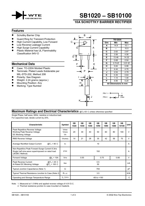
SB1020 – SB1010010A SCHOTTKY BARRIER RECTIFIERSingle Phase, half wave, 60Hz, resistive or inductive load.For capacitive load, derate current by 20%.Characteristic SymbolSB1020SB1030SB1040SB1050SB1060SB1080SB10100UnitPeak Repetitive Reverse Voltage Working Peak Reverse Voltage DC Blocking Voltage V RRMV RWMV R203040506080100VRMS Reverse Voltage V R(RMS)14212835425670V Average Rectified Output Current @T C = 95°C I O10A Non-Repetitive Peak Forward Surge Current 8.3msSingle half sine-wave superimposed on rated load(JEDEC Method)I FSM150A Forward Voltage @I F = 10A V FM0.550.750.85VPeak Reverse Current @T A = 25°C At Rated DC Blocking Voltage @T A = 100°C I RM0.550mATypical Junction Capacitance (Note 1)C j700pF Typical Thermal Resistance Junction to Case (Note 2)R JC 3.5K/W Operating and Storage Temperature Range T j, T STG-65 to +150°C Note: 1. Measured at 1.0 MHz and applied reverse voltage of 4.0V D.C.2. Thermal resistance junction to case mounted on heatsink.WTEI ,A V E R A G E O U T P U T C U R R E N T (A )(A V )024681010406080100120140150T , LEAD TEMPERATURE (ºC)Fig.1Forward Current Derating CurveL100100020000.1 1.010100C ,C A P A C I T A N C E (p F )j V ,REVERSE VOL TAGE (V)Fig.4T ypical Junction CapacitanceR 0306090120150110100I , P E A K F O R W A R D S U R G E C U R R E N T (A )F S M NUMBER OF CYCLES AT 60HzFig. 3 Maximum Non-Repetitive P eak Fwd Surge Current0.11020400.51.01.52.02.5I ,N S T A N T A N E O U S F O R W A R D C U R R E N T (A )F V ,INSTANTANEOUS FORWARD VOLTAGE (V)Fig.2T ypical Forward CharacteristicsFORDERING INFORMATIONProduct No.Package TypeShipping QuantitySB1020TO-220A 50 Units/Tube SB1030TO-220A 50 Units/Tube SB1040TO-220A 50 Units/Tube SB1050TO-220A 50 Units/Tube SB1060TO-220A 50 Units/Tube SB1080TO-220A 50 Units/Tube SB10100TO-220A50 Units/TubeShipping quantity given is for minimum packing quantity only. For minimum orderquantity, please consult the Sales Department.Won-Top Electronics Co., Ltd (WTE) has checked all information carefully and believes it to be correct and accurate. However, WTE cannot assume any responsibility for inaccuracies. Furthermore, this information does not give the purchaser of semiconductor devices any license under patent rights to manufacturer. WTE reserves the right to change any or all information herein without further notice.WARNING : DO NOT USE IN LIFE SUPPORT EQUIPMENT. WTE power semiconductor products are not authorized for use as critical components in life support devices or systems without the express written approval.We power your everyday.Won-Top Electronics Co., Ltd.No. 44 Yu Kang North 3rd Road, Chine Chen Dist., Kaohsiung, Taiwan Phone: 886-7-822-5408 or 886-7-822-5410Fax: 886-7-822-5417Email: sales@Internet: 。
RT424024中文资料

.50 (12.7)
6X .031 X .020 (.80 X .52)
2X .020 X .020 (.52 X .52)
.17 (4.3)
PC Board Layouts (Bottom View)
1 Pole 12A 3.5mm
.051 DIA. (1.30)
1 Pole 16A 2 Pole 8A 5mm
元器件交易网
s
RT series
Miniature Printed Circuit Board Relays, Sockets and Accessories
元器件交易网
Features
• SPST through DPDT contact arrangements. • Immersion cleanable and flux tight versions available. • VDE 10mm spacing, 5kV dielectric, coil to contacts. • UL Class F coil insulation system. • Conforms to UL 508, 1873, 353 and 1950. • Low profile; 15.7mm height. • Sensitive coil; 400mW. • Withstand surge voltage of 10,000V.
Resistive Resistive
Motor Motor Motor Motor Tungsten Pilot Duty Pilot Duty
Resistive/GP Resistive
Resistive/GP Resistive Motor Motor Motor Motor Pilot Duty Tungsten
CDBF0240;中文规格书,Datasheet资料

Forward current (mA )
Reverse current ( A )
100
100u 10u 1u 100n
10
75 C
1
0.1
125 C 75 C
25 C
25
C C
0.01
-25
-25 C
10n 1n
0.001 0 0.1 0.2 0.3 0.4 0.5 0.6 0.7
0
10Biblioteka 203040Forward voltage (V)
Reverse voltage (V)
Fig. 3 - Capacitance between terminals characteristics
Capacitance between terminals (pF)
100
Fig. 4 - Current derating curve
SMD Schottky Barrier Diode
RATING AND CHARACTERISTIC CURVES (CDBF0240)
Fig. 1 - Forward characteristics
1000 10m 1m
Fig. 2 - Reverse characteristics
125 C
Conditions
I F = 200 mA DC
Symbol Min Typ Max Unit
VF IR CT 0.45 1 9 0.55 10 V uA pF
F = 1 MHZ and 10 VDC reverse voltage
REV:A
QW-A1030
Page 1
/
I FSM PD T STG Tj
- 1、下载文档前请自行甄别文档内容的完整性,平台不提供额外的编辑、内容补充、找答案等附加服务。
- 2、"仅部分预览"的文档,不可在线预览部分如存在完整性等问题,可反馈申请退款(可完整预览的文档不适用该条件!)。
- 3、如文档侵犯您的权益,请联系客服反馈,我们会尽快为您处理(人工客服工作时间:9:00-18:30)。
Rev. 1.0 Aug 2, 2004 1/3
元器件交易网
ASB0240
SMD Schottky Barrier Diode Maximum Rating (at TA=25ºC unless otherwise noted)
Symbol Parameter Conditions Min Typ Max Unit
元器件交易网
ASB0240
SMD Schottky Barrier Diode Features
IO = 200mA
VR = 40V
- Designed for mounting on small surface. - Extremely thin package. - Low leakage current (IR=0.1uA typ. @VR=10V). - Majority carrier conduction. - Lead-free device
Rev. 1.0 Aug 2, 2004
元器件交易网
ASB0240
SMD Schottky Barrier Diode Rating And Characteristic Curves
125 C
75 C
25 C
-25 C
f = 1 MHz Ta = 25 C
Ambient temperature ( C )
0.010(0.25)Typ. 0.033(0.85) 0.028(0.70)
General Description
0603(1608)
0.071(1.80) 0.063(1.60) 0.039(1.00) 0.031(0.80)
0.012(0.30)Typ.
0.014(0.35)Typ. Dimensions in inches and (millimeter)
BF:0.006gram (approximately)
Ordering information
A XX XX XX XX
Feature SB : Schottky Barrier
lo
Vo
Package type BD-0603 BF-1005
This datasheet contains new product information. Anachip Corp. reserves the rights to modify the product specification without notice. No liability is assumed as a result of the use of this product. No rights under any patent accompany the sale of the product.
- Weight : BD:0.003gram (approximately)
0.014(0.35)Typ. 0.014(0.35)Typ.
0.051(1.30) 0.043(1.10)
0.035(0.90) 0.027(0.70)
0.012(0.30)Typ.
Hale Waihona Puke Dimensions in inches and (millimeter)
VRRM VR IO IFSM PD TSTG Tj
Repetitive peak reverse voltage Reverse voltage Average forward current Forward current, surge peak Power Dissipation Storage temperature Junction temperature 0603 1005 0603 1005 8.3ms single half sine-wave superimposed on rate load (JEDEC method)
Marking Information
B7 ASB0240
Anachip Corp. 3/3
Rev. 1.0 Aug 2, 2004
VF IR CT
Forward voltage Reverse current Capacitance between terminals
IF=200mADC VR=10V F=1MHz, and 10 VDC reverse voltage
-
0.45 9
0.55 1 -
V µA pF
Anachip Corp. 2/3
-40 -40
2000 3000 -
45 40 200 150 250 +125 +125
V V mA mA mW ºC ºC
Electrical Characteristics (at TA=25ºC unless otherwise noted)
Symbol Parameter Conditions Min. Typ. Max. Unit
P+
1005(2512)
0.102(2.60) 0.095(2.40)
Mechanical Data
- Case :0603(1608) 1005(2512) standard package, molded plastic. - Terminals : Gold plated, solderable per MIL-STD-750, method 2026. - Polarity : Indicated by cathode band. - Mounting position : Any.