LDS-A514RI, 规格书,Datasheet 资料
LDSBus Trailing Edge Light Dimmer Datasheet说明书

LDSBus Trailing Edge Light Dimmer DatasheetVersion 1.0Document Reference No.: BRT_000380 Clearance No.: BRT#1901 Introduction1.1 FeaturesNeither the whole nor any part of the information contained in, or the product described in this manual, may be adapted or reproduced in any material or electronic form without the prior written consent of the copyright holder. This product and its documentation are supplied on an as-is basis and no warranty as to their suitability for any particular purpose is either made or implied. Bridgetek Pte Ltd will not accept any claim for damages howsoever arising as a result of use or failure of this product. Your statutory rights are not affected. This product or any variant of it is not intended for use in any medical appliance, device or system in which the failure of the product might reasonably be expected to result in personal injury. This document provides preliminary information that may be subject to change without notice. No freedom to use patents or other intellectual property rights is implied by the publication of this document. Bridgetek Pte Ltd, 178 Paya Lebar Road, #07-03, Singapore 409030. Singapore Registered Company Number: 201542387HLDSBus Trailing Edge LightDimmerDatasheetLDSBus Trailing Edge Light Dimmer can be integrated with dimmable LED lamps for adjusting the percentage of light dimming. Our trailing edge technology uses a current that is turned off when the AC waveform ends . The operation is smoother, soft starting and silent. It can control up to 550W@240VAC or 230W@100VAC for single-change loading.The LDSBus Trailing Edge Light Dimmer has a 2 digit display to show the percentage of dimmin g .Zero crossing detection determines whether the AC input frequency is 50Hz or 60Hz before enabling dimming.Additionally, an external dimmer controller can be used to control light dimming.∙Suitable for dimmable LEDs and lamps with single channel AC inputs and loading∙Trailing edge AC control to provide smooth dimming control∙Detects zero crossings and produces symmetrical pulses around them∙ LED indicators indicate 50Hz or 60Hz AC∙ 2 Digit dimming percentage display∙UP/DOWN push buttons for manual override of dimming∙Support for external dimmer control with UP/DOWN connectors∙ Bridgetek LDSBus protocol. Data/power transmission via the LDSBus HVT-Junction ∙ Low power consumption∙Operating temperature range : 0o C to +55o C∙ Flush mount and DIN Rail mounting options∙ Supported platforms: Bridgetek IoTPortal,PanL Smart Living and LDSBus Python SDK Visit http://bit.ly/ldsbus-resources for more information2Part NumbersTable of Contents1Introduction (1)1.1Features (1)2Part Numbers (2)3Product Specifications (4)4Hardware Features (5)5Configuration and Installation (6)6Mounting Options (7)6.1Flush Mount (7)6.2DIN Rail Mount (7)7Terminal Wiring Instructions on AC Input & Output .. 8 7.1AC Input and Output Setup (9)8Terminal Wiring Instructions on External DimUp/Down (10)8.1External Dimming Up/Down Setup (11)9LED Display (12)10Mechanical Dimension (13)11Contact Information (14)Appendix A – References (15)Document References (15)Acronyms and Abbreviations (15)Appendix B – List of Tables & Figures (16)List of Tables (16)List of Figures (16)Appendix C – Revision History (17)3Product SpecificationsTable 1 - LDSBus Trailing Edge Light Dimmer Specifications4 Hardware FeaturesFigure 1 - LDSBus Trailing Edge Light Dimmer Controller2 Digit Display & LEDIndicatorAC Input AC OutputDimming Push Buttons (Up/Down)RJ12 LDSU Flush MountingSlotExternal DimmingConnectorDIN Rail Plate5Configuration and InstallationPlease visit http://bit.ly/ldsbus-resources to access the LDSBus Configuration Utility guide on how to configure the device name, device address and termination settings before using it for your application.5.1Connection DiagramFigure 2 illustrates the connection of the LDSBus Trailing Edge Light Dimmer (LDSBus Device) to the LDSBus. Please visit http://bit.ly/ldsbus-resources to view the full device application, setup and installation guides.Figure 2 - LDSBus Trailing Edge Light Dimmer - Connection DiagramSetup Instructions:1.Connect the first LDSBus HVT-Junction to any of the LDSBus Host Systems using aRJ45(CAT5e) cable.2.Connect the configured LDSBus Trailing Edge Light Dimmer to the LDSBus HVT-Junction asshown in Figure 2.3.If there is more than one LDSBus HVT-Junction, chain them together as shown in Figure 2.4.Enable terminator for the last device in LDSBus.6 Mounting Options6.1 Flush MountThe LDSBus Trailing Edge Light Dimmer can be flush mounted directly on a wall or any flat surface using 2 M3.5*16mm (thread) screws.Figure 3 - LDSBus Trailing Edge Light Dimmer Flush Mount6.2 DIN Rail MountThe DIN Rail Mount can be fixed using a DIN Rail bracket that has two mounting holes. The package includes mounting screws and a backplate. (The DIN Rail Bracket is not included in the package).Figure 4 - LDSBus Trailing Edge Light Dimmer DIN Rail MountDIN Rail Mount 2xM3.5*16mm7 Terminal Wiring Instructions on AC Input & OutputThe connections are made with Push-in CAGE CLAMP technology. When using solid conductor wire or stranded wire insulation ferrule, the stripped conductor can simply be inserted into the clamp until it hits the backstop without requiring a screwdriver. Figure 5 shows how to remove the cable from the connector using a flat head screwdriver to push the push buttons and pull out the wire.Figure 5 - Push-in Wire and Pull-out WireTable 2 provides a list of American Wire Gauges (AWGs) that can be used in the Terminal Blocks on AC Input and Output load.As shown in Figure 6, the wire strip is 8mm to 12mm long.Figure 6 - 8mm to 12mm wire strip8mm ~ 12mm7.1 AC Input and Output SetupThe AC terminals support AC 100VAC – 240VAC input and dimmable lights and LEDs on the output. The connection is illustrated below:Note: Ensure that the dimmable light/LED is compatible with the AC voltage connected to the input terminal when selecting it.8 Terminal Wiring Instructions on External DimUp/DownThe terminal block is connected by screws. Figure 7 shows how to clamp the wire using a 0.4mm x 2.5mm slotted screwdriver and rotate in a clockwise direction. To release the wire, turn anticlockwise.Figure 7 - Clamping wire with screwdriver in clockwise directionTable 3 provides a list of American Wire Gauges (AWGs) that can be used in Terminal Blocks on External Dim Up / down.As shown in Figure 8, the wire strip is 3mm to 5mm long.Figure 8 - 3mm to 5mm wire strip3mm ~ 5mm8.1External Dimming Up/Down SetupA dimmable external connector supports UP / DOWN dimming. The connection is illustrated below:9LED DisplayTable 4 - LDSBus Trailing Edge Light Dimmer – LED DisplayA 7-segment LED in the controller indicates the brightness percentage when used with an external host application e.g. Bridgetek IoTPortal, LDSBus Python SDK or PanL Smart Living. The LED displays the internal PWM percentage when using the on-board buttons or external dimming interface. When an application sets the brightness, the display returns to brightness percentage.10.060.010.0 60.0 10 Mechanical DimensionFigure 9 - LDSBus Trailing Edge Light Dimmer Dimension – Top ViewFigure 10 - LDSBus Trailing Edge Light Dimmer Dimension – Side ViewFigure 11 - LDSBus Trailing Edge Light Dimmer Dimension – Bottom View138.2 126.7 76.0138.2126.776.041.741.711Contact InformationHead Quarters – Singapore Branch Office – Taipei, TaiwanBridgetek Pte Ltd178 Paya Lebar Road, #07-03 Singapore 409030Tel: +65 6547 4827Fax: +65 6841 6071Bridgetek Pte Ltd, Taiwan Branch2 Floor, No. 516, Sec. 1, Nei Hu Road, Nei Hu District Taipei 114Taiwan, R.O.C.Tel: +886 (2) 8797 5691Fax: +886 (2) 8751 9737E-mail (Sales)**********************E-mail (Sales)**********************E-mail (Support)************************E-mail (Support)************************ Branch Office - Glasgow, United Kingdom Branch Office – VietnamBridgetek Pte. Ltd.Unit 1, 2 Seaward Place, Centurion Business Park Glasgow G41 1HHUnited KingdomTel: +44 (0) 141 429 2777Fax: +44 (0) 141 429 2758Bridgetek VietNam Company LimitedLutaco Tower Building, 5th Floor, 173A Nguyen Van Troi,Ward 11, Phu Nhuan District,Ho Chi Minh City, VietnamTel : 08 38453222Fax : 08 38455222E-mail (Sales)***********************E-mail (Sales)**********************E-mail (Support)************************E-mail (Support)************************Web Site/Distributor and Sales RepresentativesPlease visit the Sales Network page of the Bridgetek Web site for the contact details of our distributor(s) and sales representative(s) in your country.System and equipment manufacturers and designers are responsible to ensure that their systems, and any Bridgetek Pte Ltd (BRTChip) devices incorporated in their systems, meet all applicable safety, regulatory and system-level performance requirements. All application-related information in this document (including application descriptions, suggested Bridgetek devices and other materials) is provided for reference only. While Bridgetek has taken care to assure it is accurate, this information is subject to customer confirmation, and Bridgetek disclaims all liability for system designs and for any applications assistance provided by Bridgetek. Use of Bridgetek devices in life support and/or safety applications is entirely at the user’s risk, and the user agrees to defend, indemnify and hold harmless Bridgetek from any and all d amages, claims, suits or expense resulting from such use. This document is subject to change without notice. No freedom to use patents or other intellectual property rights is implied by the publication of this document. Neither the whole nor any part of the information contained in, or the product described in this document, may be adapted or reproduced in any material or electronic form without the prior written consent of the copyright holder. Bridgetek Pte Ltd, 178 Paya Lebar Road, #07-03, Singapore 409030. Singapore Registered Company Number: 201542387H.Appendix A – References Document ReferencesLDSBus Configuration Utility Guide Acronyms and AbbreviationsAppendix B – List of Tables & FiguresList of TablesTable 1 - LDSBus Trailing Edge Light Dimmer Specifications (4)Table 2 - AWG to use in terminal block on AC Input and Output load (8)Table 3 - AWG to use in terminal blocks on external Dim up/down (10)Table 4 - LDSBus Trailing Edge Light Dimmer – LED Display (12)List of FiguresFigure 1 - LDSBus Trailing Edge Light Dimmer Controller (5)Figure 2 - LDSBus Trailing Edge Light Dimmer - Connection Diagram (6)Figure 3 - LDSBus Trailing Edge Light Dimmer Flush Mount (7)Figure 4 - LDSBus Trailing Edge Light Dimmer DIN Rail Mount (7)Figure 5 - Push-in Wire and Pull-out Wire (8)Figure 6 - 8mm to 12mm wire strip (8)Figure 7 - Clamping wire with screwdriver in clockwise direction (10)Figure 8 - 3mm to 5mm wire strip (10)Figure 9 - LDSBus Trailing Edge Light Dimmer Dimension – Top View (13)Figure 10 - LDSBus Trailing Edge Light Dimmer Dimension – Side View (13)Figure 11 - LDSBus Trailing Edge Light Dimmer Dimension – Bottom View (13)Appendix C – Revision HistoryDocument Title: LDSBus Trailing Edge Light Dimmer Datasheet Document Reference No.: BRT_000380Clearance No.: BRT#190Product Page: https:///ldsbus/Document Feedback: Send Feedback。
514中文说明书
. /_
/_ μ 8 ܖ
ˏ ၠූ
-
ၠ
-
p
p ඪ/_
-) )
d,- $ (-e
ඪ /_ ऋķś
ݖķś Ĝ×-
)- /_ " " " " O %%. ቱූ ´t) ቱූ #/ ݖ Oቱූ Ĝ×-
操作前的准备
基本接线图
①、推荐“0V/公共端”接地,若一个系统中有多台调速器,请将所有的”0V/公共端”连接在一起 一点接地. ②、当调速器使用电流控制时,端子 14 和 15 需要短接作为堵转过载信号。
ȩ
Ĝ
ҧ 2 // s Ƒؽ
!! !! !! ' !! ' !! !! 8 h !! ࢠ֧ Ѥ !! ๛ ඥ Ѥ V (! $)* + Ѥ !! ๛ ඥ Ѥ V (! $)* + Ѥ !! ๛ ඥ Ѥ V (! $)* + , Ѥ V (! $)* + , Ѥ V (! $)* + !! ' !! '
జnj
Ȓ̵O
ඥ ffffffffffffffffffffffff ඥ ffffffffffffffffffff Ѥ-fffffffffffffffffffffffff Ѥᇍfffffffffffffffffff -˫fffffffffffffffffffffffff ঠѤfffffffffffffffffffffffff ͵ Ѥfffffffffffffffffffffffff ᇏW8 Ѥfffffffffffffffffffffff njᇕ fffffffffffffffffffffffff < ͩ$ ᇍfffffffffffffffffff
74AHC1G14SE-7,74AHC1G14SE-7,74AHC1G14SE-7,74AHC1G14W5-7,74AHC1G14W5-7, 规格书,Datasheet 资料
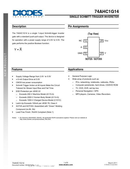
DescriptionThe 74AHC1G14 is a single 1-input Schmitt-trigger inverter gate with a standard push-pull output. The device is designed for operation with a power supply range of 2.0V to 5.5V. The gate performs the positive Boolean function:AY =Pin AssignmentsSOT25 / SOT353NCGND YVcc(Top View)AFeatures• Supply Voltage Range from 2.0V to 5.5V • ± 8 mA Output Drive at 5.0V • CMOS low power consumption• Schmitt Trigger Action at All Inputs Make the Circuit Tolerant for Slower Input Rise and Fall Time. •ESD Protection per JESD 22o Exceeds 200-V Machine Model (A115-A) o Exceeds 2000-V Human Body Model (A114-A) o Exceeds 1000-V Charged Device Model (C101C) • Latch-Up Exceeds 100mA per JESD 78, Class II • SOT25 and SOT353: Assembled with “Green” Molding Compound (no Br, Sb)• Lead Free Finish / RoHS Compliant (Note 1)Applications• General Purpose Logic •Wide array of products such as:o PCs, networking, notebooks, netbooks, PDAs o Computer peripherals, hard drives, CD/DVD ROM o TV, DVD, DVR, set top box o Personal Navigation / GPSo MP3 players ,Cameras, Video RecordersNotes: 1. EU Directive 2002/95/EC (RoHS). All applicable RoHS exemptions applied. Please visit our website at/products/lead_free.html .Pin DescriptionsPin NamePin NO.DescriptionNC 1 NoConnection A 2 Data Input GND 3 Ground Y 4 Data OutputV CC 5 Supply VoltageLogic DiagramFunction TableInputs Output AYH L L HAbsolute Maximum Ratings (Note 2)Symbol Description Rating UnitESD HBM Human Body Model ESD Protection 2 KVESD CDM Charged Device Model ESD Protection 1 KVESD MM Machine Model ESD Protection 200 V V CC Supply Voltage Range -0.5 to 6.5 VV I Input Voltage Range -0.5 to 6.5 VV O Voltage applied to output in high or low state -0.5 to V CC +0.5 VI IK Input Clamp Current V I<0 -20 mAI OK Output Clamp Current (V O < 0 or V O > V CC) ±20 mAI O Continuous output current (V O = 0 to V CC) ±25 mAI CC Continuous current through V CC 50 mAI GND Continuous current through GND -50 mAT J Operating Junction Temperature -40 to 150 °CT STG Storage Temperature -65 to 150 °CNotes: 2. Stresses beyond the absolute maximum may result in immediate failure or reduced reliability. These are stress values and device operation should bewithinrecommendvalues.Recommended Operating Conditions (Note 3)Symbol Parameter Min Max UnitV CC Operating Voltage 2 5.5 V V I Input Voltage 0 5.5 VV O Output Voltage 0 V CC VI OH High-level output current V CC = 2V -50 uA V CC = 3.3V ± 0.3V -4mAV CC = 5V ± 0.5V -8I OL Low-level output current V CC = 2V 50 uA V CC = 5V ± 0.5V 4mAV CC = 3V 8T A Operating free-airtemperature-40 125 ºCNotes: 3. Unused inputs should be held at V CC or Ground.Electrical CharacteristicsSymbol Parameter Test Conditions V CC25ºC -40ºC to 85ºC -40ºC to 125ºCUnit Min Typ. Max Min Max Min MaxV T+Positive-goinginputthresholdvoltage3V 2.2 2.2 2.2 V4.5V 3.15 3.15 3.15 V5.5V 3.85 3.85 3.85 VV T-Negative-goinginputthresholdvoltage3 V 0.9 0.9 0.9 V4.5V 1.35 1.35 1.35 V5.5V 1.65 1.65 1.65 VΔV T Hysteresis(V T+ - V T-)3V 0.3 1.2 0.3 1.2 0.25 1.2 V4.5V 0.4 1.4 0.4 1.4 0.35 1.4 V5.5V 0.5 1.6 0.5 1.6 0.45 1.6V OH High LevelOutput VoltageI OH = -50μA2V 1.9 2 1.9 1.9V3V 2.9 3 2.9 2.94.5V 4.4 4.5 4.4 4.4I OH = -4mA 3V 2.58 2.48 2.40I OH = -8mA 4.5V 3.94 3.8 3.70V OL Low LevelOutput VoltageI OL = 50μA2V 0.1 0.1 0.1V3V 0.1 0.1 0.14.5V 0.1 0.1 0.1I OL = 4mA 3V 0.36 0.44 0.55I OL = 8mA 4.5V 0.36 0.44 0.55I I Input Current V I = 5.5 V or GND 0 to 5.5V± 0.1 ± 1 ± 2 μAI CC Supply Current V I = 5.5V or GNDI O=05.5V 1 10 40 μAC I InputCapacitanceV I = V CC – orGND5.5V 2.0 10 10 10 pFθJA ThermalResistanceJunction-to-AmbientSOT25(Note 4)195o C/W SOT353 430θJC ThermalResistanceJunction-to-CaseSOT25(Note 4)58o C/W SOT353 155Note: 4. Test conditions for SOT25, and SOT353: Device mounted on FR-4 substrate PC board, 2oz copper, with minimum recommended pad layoutSwitching CharacteristicsV CC = 3.3V ± 0.3 (see Figure 1)ParameterFrom (Input) TO (OUTPUT)25ºC -40ºC to 85ºC -40ºC to 125ºCUnitMinTyp.MaxMin Max Min Maxt pdA YC L =15pF0.6 4.2 12.8 0.6 15.0 0.6 16.5 ns C L =50pF0.6 6.0 16.3 0.6 18.5 0.6 20.5 nsV CC = 5V ± 0.5V (see Figure 1)ParameterFrom (Input) TO (OUTPUT)25ºC -40ºC to 85ºC -40ºC to 125ºCUnitMinTyp.MaxMin MaxMin Maxt pdA YC L =15pF0.6 3.2 8.6 0.6 10.0 0.6 11.0 ns C L =50pF0.6 4.6 10.6 0.6 12.0 0.6 13.5 nsOperating CharacteristicsT A = 25 ºCParameterTest Conditions V CC = 5 V Unit Typ. C pdPower dissipation capacitancef = 1 MHz No Load10pFParameter Measurement InformationV CCInputsV M C LVIt r /tf3.3V±0.3VV CC ≤3ns V CC /2 15pF 5V±0.5V V CC ≤3ns V CC /2 15pF 3.3V±0.3V V CC ≤3ns V CC /2 50pF 5V±0.5VV CC≤3nsV CC /250pFVoltage Waveform Pulse DurationVoltage Waveform Propagation Delay TimesInverting and Non Inverting OutputsFigure 1. Load Circuit and Voltage WaveformsNotes: A. Includes test lead and test apparatus capacitance.B. All pulses are supplied at pulse repetition rate ≤ 1 MHz.C. Inputs are measured separately one transition per measurement.D. t PLH and t PHL are the same as t PD .Ordering Information74AHC1G 14XX -7W5:SOT25FunctionPackage7:Tape &ReelPacking 14:1-InputSchmitt-Trigger InverterSE :SOT353Logic Device 74:Logic Prefix AHC :2to Family 1G :One gate5.5VDevice Package Code Packaging (Note 5) 7” Tape and ReelQuantityPart Number Suffix74AHC1G14W5-7 W5 SOT25 3000/Tape & Reel -7 74AHC1G14SE-7SESOT3533000/Tape & Reel-7Notes: 5. Pad layout as shown on Diodes Inc. suggested pad layout document AP02001, which can be found on our website at/datasheets/ap02001.pdf.Marking InformationXX : Identification codeW : Week : A~Z : 1~26 week;X : A~Z : Internal code(Top View)Y : Year 0~9a~z : 27~52 week; z represents 52 and 53 weekPart NumberPackageIdentification Code74AHC1G14W5 SOT25 YV 74AHC1G14SE SOT353YVPackage Outline Dimensions (All Dimensions in mm) (1) Package Type: SOT25(2) Package Type: SOT353SOT25Dim Min Max TypA0.350.500.38B 1.50 1.70 1.60C 2.70 3.00 2.80D ⎯ ⎯ 0.95H 2.90 3.10 3.00J0.0130.100.05K 1.00 1.30 1.10L0.350.550.40M0.100.200.15N0.700.800.75α 0° 8° ⎯All Dimensions in mmSOT353Dim Min MaxA0.10 0.30B 1.15 1.35C 2.00 2.20D0.65 TypF0.40 0.45H 1.80 2.20J0 0.10K0.90 1.00L0.25 0.40M0.10 0.22α 0° 8°All Dimensions in mm。
MOV-14D201K,MOV-14D431K,MOV-14D471K,MOV-14D181K,MOV-14D391K,MOV-14D511K, 规格书,Datasheet 资料
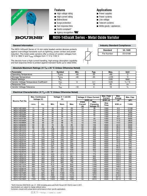
*RoHS Directive 2002/95/EC Jan. 27, 2003 including annex and RoHS Recast 2011/65/EU June 8, 2011. Specifi cations are subject to change without notice.Customers should verify actual device performance in their specifi c applications.Absolute Maximum Ratings (@ T A = 25 °C Unless Otherwise Noted)ParameterSymbol Min.Typ.Max.Unit Operating Temperature T OPR -4025+85˚C Storage Temperature T STG -4025+125˚C Rated WattageP w 0.60Watt Varistor Voltage Temperature Coeffi cient V TC 00.10.05 % / ˚C Response TimeT r 1025ns Varistor Voltage ToleranceV tol-1010%Electrical Characteristics (@ T A = 25 °C Unless Otherwise Noted)*Ro H S C O MP L I A N TBourns Part No.Max. Continuous Voltage (V)Voltage @ 1 mA DC(V)Voltage @ Class Current Max. PeakCurrent Max.Energy Max. Cap.(8/20 μs)(8/20 μs)(J)(pF)r.m.s.d.c.Min.Nom.Max.ClassCurrent(A)Max.Clamping Voltage (V)One Time 8/20 μs 1 kHz MOV-14D180K 111416182010361000 4.011100MOV-14D220K 141820222410431000 5.09100MOV-14D270K 172224273010531000 6.07400MOV-14D330K 2026303336106510007.56100MOV-14D390K 2531353943107710008.65100MOV-14D470K 30384247521093100010.04300MOV-14D560K 354550566210110100011.03600MOV-14D680K 405661687510135100014.02900MOV-14D820K 506574829050135450022.02400MOV-14D101K 60859010011050165450028.02000MOV-14D121K 7510010812013250200450032.01700MOV-14D151K 9512513515016550250450040.01300MOV-14D181K 11515016218019850300450050.01100MOV-14D201K 13017018520022550340450057.01000MOV-14D221K 14018019822024250360450060.0900MOV-14D241K 15020021624026450395450063.0830MOV-14D271K 17522524327029750455450070.0740MOV-14D301K 19025027030033050500450077.0670MOV-14D331K 21027529733036350550450085.0610MOV-14D361K 23030032436039650595450093.0560MOV-14D391K 250320351390429506504500100.0510MOV-14D431K 275350387430473507104500115.0460MOV-14D471K 300385423470517507754500125.0430MOV-14D511K 320415459510561508454500125.0390MOV-14D561K 350460504560616509254500125.0360MOV-14D621K 3855055586206825010254500125.0320MOV-14D681K 4205606126807485011204500130.0290MOV-14D751K 4606156757508255012404500143.0270MOV-14D781K 4856407027808585012904500148.0260MOV-14D821K 5106707388209025013554500157.0240MOV-14D911K 55074581991010015015004500175.0220MOV-14D102K 625825900100011005016504500190.0200MOV-14D112K 680895990110012105018154500213.0180MOV-14D152K 7509901080150013205019804500337.0150MOV-14D182K110014651620180019805029704500337.010014D 201K5Specifi cations are subject to change without notice.Customers should verify actual device performance in their specifi c applications.Product DimensionsDIMENSIONS:MM(INCHES)This is an RoHS compliant molded radial package with 100 % Sn plating on the terminations.Internal ConstructionHow to OrderMOV - 14D nn (n) K (TR)Model DesignatorMOV = Metal Oxide Varistor Disc Diameter 14D = 14 mmNominal Varistor VoltageSee Electrical Characteristics TableMultiplier of Voltage Digits 0 = No multiplier 1 = nn * 101 2 = nn * 102Varistor Voltage Tolerance K = 10 %PackagingBlank = BulkTR = Tape & Reel*Examples: MOV-14D270K = 27 V, Bulk PackMOV-14D331KTR = 330 V, T ape & Reel* Models MOV-14D911K, 102K, 112K, 152K and 182K are not available in Tape & Reel packaging.Part Number Dim. H (Max.)Dim. T (Max.)MOV-14D180K20.0(.787) 3.8(.150)MOV-14D220K 20.0(.787) 3.9(.154)MOV-14D270K 20.0(.787) 4.2(.165)MOV-14D330K 20.0(.787) 3.8(.150)MOV-14D390K20.0(.787) 4.0(.157)MOV-14D470K 20.0(.787) 4.2(.165)MOV-14D560K 20.0(.787) 4.3(.169)MOV-14D680K 20.0(.787) 4.4(.173)MOV-14D820K20.0(.787) 3.8(.150)MOV-14D101K 20.0(.787) 4.0(.157)MOV-14D121K20.0(.787) 4.2(.165)MOV-14D151K 20.0(.787) 4.4(.173)MOV-14D181K20.0(.787) 3.6(.142)MOV-14D201K 20.0(.787) 3.8(.150)MOV-14D221K 20.0(.787) 3.9(.154)MOV-14D241K 20.0(.787) 4.0(.157)MOV-14D271K 20.0(.787) 4.2(.165)MOV-14D301K20.0(.787) 4.4(.173)Part Number Dim. H (Max.)Dim. T (Max.)MOV-14D331K 20.0(.787) 4.6(.181)MOV-14D361K 20.0(.787) 4.8(.189)MOV-14D391K 20.0(.787) 5.0(.197)MOV-14D431K 20.0(.787) 5.2(.205)MOV-14D471K 20.0(.787) 5.4(.213)MOV-14D511K 20.0(.787) 5.5(.217)MOV-14D561K 22.0(.866) 6.0(.236)MOV-14D621K 22.0(.866) 6.4(.252)MOV-14D681K 22.0(.866) 6.5(.256)MOV-14D751K 22.0(.866) 6.7(.264)MOV-14D781K 22.0(.866) 6.9(.272)MOV-14D821K 22.0(.866)7.3(.287)MOV-14D911K*22.0(.866)7.7(.303)MOV-14D102K*22.0(.866)8.2(.323)MOV-14D112K*22.0(.866)8.7(.343)MOV-14D152K*22.0(.866)9.7(.382)MOV-14D182K*22.0(.866)11.7(.461)* Not available in Tape & Reel packaging.Specifi cations are subject to change without notice.Customers should verify actual device performance in their specifi c applications.1011001000101010101010Current (A)V o l t a g e (V )680560470390330270220180100100010000101010101010Current (A)V o l t a g e (V )18215211210291182178175168162156151147110010100010000101010101010Current (A)V o l t a g e (V )431391361331301271241221201181151121101820101010101010101010101010101010Performance Graphs V-I CharacteristicsMOV-14D180K to MOV-14D680KMOV-14D820K to MOV-14D431KMOV-14D471K to MOV-14D182KBournsPart Number Bourns Part Marking MOV-14D180K 14D180K MOV-14D220K 14D220K MOV-14D270K 14D270K MOV-14D330K 14D330K MOV-14D390K 14D390K MOV-14D470K 14D470K MOV-14D560K 14D560K MOV-14D680K 14D680K MOV-14D820K 14D820K MOV-14D101K 14D101K MOV-14D121K 14D121K MOV-14D151K 14D151K MOV-14D181K 14D181K MOV-14D201K 14D201K MOV-14D221K 14D221K MOV-14D241K 14D241K MOV-14D271K 14D271K MOV-14D301K 14D301K MOV-14D331K 14D331K MOV-14D361K 14D361K MOV-14D391K 14D391K MOV-14D431K 14D431K MOV-14D471K 14D471K MOV-14D511K 14D511K MOV-14D561K 14D561K MOV-14D621K 14D621K MOV-14D681K 14D681K MOV-14D751K 14D751K MOV-14D781K 14D781K MOV-14D821K 14D821K MOV-14D911K 14D821K MOV-14D102K 14D102K MOV-14D112K 14D112K MOV-14D152K 14D152K MOV-14D182K14D182KNOTE: The “5” marking on MOV products is for traceability of production assembly for quality assurance compliance.Typical Part MarkingPackaging InformationTAPE & REELItem Symbol14 mm Disc Reel Outside Diameter RD355(13.98) Reel Inner Diameter RD130(11.81) Tape Width RW55(2.165) Reel Width RW163(2.48) Pitch of Component P25.4 ± 1.0(1.00 ± 0.04) Feed Hole Pitch P012.7 ± 1.0(0.50 ± 0.04) Feed Hole Center to Pitch P18.95 ± 0.7(0.352 ± 0.3) Feed Hole Center to ComponentCenterP212.7 ± 1.0(0.50 ± 0.04)Lead to Lead Distance F7.50 ± 0.8(0.30 ± 0.03)Component AlignmentΔh4.0max.(0.157) max.Tape Width W18.0 ± 0.5(0.71 ± 0.02)Hole Down Tape Width W012.0 ± 0.8(0.47 ± 0.03)Hole Position W19.0 ± 0.5(0.35 ± 0.02)Hole Down Tape Position W23.0max.(0.12) max.Height From Center toComponent BaseH19.0 ± 1.0(0.75 ± 0.04)Seating Plane Height H016.0 ± 0.5(0.63 ± 0.02)Component Height H140.0max.(1.57) maxCrimp Length C2.60typ.(0.10) maxFeed Hole Diameter D04.0 ± 0.2(0.16 ± 0.08)Total Tape Thickness t0.6 ± 0.3(0.02 ± 0.01)Length of Clippped Height L1.0max.(0.04) maxQuantity per ReelMOV-14D180K – 14D391KMOV-14D431K - 14D182K-100050012/11Specifi cations are subject to change without notice.Customers should verify actual device performance in their specifi c applications.BULK60.0(2.36)Asia-Pacifi c:Tel: +886-2 2562-4117Fax: +886-2 2562-4116Europe:Tel: +41-41 768 5555Fax: +41-41 768 5510The Americas:Tel: +1-951 781-5500Fax: +1-951 781-5700NOTE: Models MOV-14D911K, 102K, 112K, 152K and 182K are not availablein Tape & Reel packaging.。
安浩芯-SGD5141XX-无线充电(带锂电保护)接收芯片-规格说明书
规格说明书SGD5141XX无线充电(带锂电保护)接收芯片版本1.5 安 浩 芯保留不预先通知而修改此文件的权利目录1.概述 (3)2.特性 (3)3.引脚说明 (4)4.功能模块框图 (5)5.封装尺寸图 (6)6.编号说明 (7)7.应用电路图 (8)8.无线充电 (9)9.通信功能 (9)10.状态指示 (9)11.过温保护功能 (10)12.过流、短路保护和自动恢复功能 (10)13.过放电保护功能 (11)14.极限工作条件 (11)15.电气参数 (12)16.修改记录 (13)1. 概述SGD5141是一款无线充电接收+锂电保护芯片,其集成通讯、高频整流、频率控制、充电状态指示、过温保护、过流保护、锂电保护等功能,外围器件精简到只需要一个小电容,带上模拟混合数字的技术,使整机可靠性更高,应用更加灵活简洁。
在小体积的产品上应用更加有优势和效率更高。
应用范围广:数码产品(智能手表、手环、耳机……),以及各类需要防水、外观讲究和充电方便的手持产品。
2. 特性◆内置的功率级采用低电阻NMOS FET技术确保高效率与低功耗◆内置模拟+数字解调,减少外围器件,通讯更加可靠灵活◆充电状态和电池状态可以给指示◆免调试,自动连接◆自动功率控制◆过热保护功能(OTP)◆欠压保护功能(UVLO)◆过流保护功能(OCP)◆短路保护功能(SCP)◆外围电路简单到一个电容,体积小,安装方便◆静态电流小于6uA,过放电保护后电流小于1uA◆电池保护功能◆充电电压检测精度高◆锂电保护◆多芯片并联,增加充电电流3. 引脚说明SOT23-6:DFN6L(2*2)4. 功能模块框图5. 封装尺寸图SOT23-6DFN6L(2mm*2mm)DFN6L(0202X0.75-0.65) 封装尺寸图6.编号说明封装形式:S表示SOT23-6充电电流:1表示100mA充电结束电压:4表示4.2V表示无线接收IC品牌7.应用电路图单芯片电路图并联芯片电路1、C1电容尽量靠近芯片,到芯片VDD和GND的走线尽量短和粗,如果电池的引线比较长,那么要加大C1的容量2、C1电容请使用NPO电容3、电池的引线到芯片的VDD和GND尽量短和粗4、由于采用的是高频磁耦合传输电能,为了减少高频的趋肤效应,用铜线绕制线圈时,可以采用多股线,画PCB或FPC时用双面板而且走线尽量宽5、LAYOUT时注意,跟芯片底部金属和GND引脚相连的铜皮尽量大和厚,目的这样可以帮助芯片散热和减低导通内阻,从而增加转换效率和提高系统的稳定性8.无线充电芯片内部集成无线充电管理电路,VCHG端口跟接收线圈相连,发射线圈发生的交变磁场,会使放在附近的接收线圈接收到AC信号,芯片内部的高压整流电路会把接收到AC信号整理成DC电源提供给电池充电,当电池电压小于2.7V时实行涓流充电,大于2.7V实现恒流充电,充电到电池电压大约4.15V时,会转成类似恒压的涓充,充电到4.2V时结束充电,充电结束电压精度是1%。
5050(GRBW)规格书白光(中文)
Rev.: A
Prepared date: 2015-11-6
Prepared by: calvin chai
Page: 5 of 6
Technical Data Sheet 5050 Top View LEDs
■ 使用说明
1. 过电流保护 客户必须使用电阻来保护,否则电压的漂移会引起电流的大幅度改变 (发生击穿现象). 灯珠使用时电流必须在规定范围之内,避免电流过大造成不良。
Rev.: A
Prepared date: 2015-11-6
发光颜色 红光 绿光 蓝光 白光
表面胶体颜色 白色透明 黄色胶体
Prepared by: calvin chai
Page: 2 of 6
Technical Data Sheet 5050 Top View LEDs
■ 封装尺寸
1. 所有标注尺寸的单位均为毫米 2. 除了特别注明,所有标注尺寸的公差均为±0.10mm
Engineer
Client affirm
Design by 工程部
Date 2015-11-30
深圳市威能照明有限公司
地址: 深圳市宝安区沙井镇新和大道丽城工业园 A 栋 邮编(Postal Code):518000 电话(TEL):0755-27336178 传真(FAX):0755-27336179
█ 绝对最大额定值(Ta = 25℃)
参数
符号
正向电流
IF
峰值正向电流(Duty 1/10 @1KHz)
IFP
功耗
Pd
操作温度
Topr
保存温度
Tstg
回流焊最高温度
Tsol
反向电压
VR
FGA25N120FTD;中文规格书,Datasheet资料

@ TC = 25oC @ TC = 100oC
Diode continuous Forward current Maximum Power Dissipation Maximum Power Dissipation Operating Junction Temperature
@ TC = 100oC @ TC = 25oC @ TC = 100oC
Symbol
Parameter
Test Conditions
VFM
Diode Forward Voltage
IF = 25A
TC = 25oC TC = 125oC
trr
Diode Reverse Recovery Time
TC = 25oC TC = 125oC
Irr
Diode Reverse Recovery Time
©2009 Fairchild Semiconductor Corporation
1
FGA25N120FTD Rev. A1
G
E
Ratings
1200 ± 25 50 25 75 25 313 125 -55 to +150 -55 to +150 300
Units
V V A A A A W W oC oC
Applications
• Induction heating and Microvewave oven • Soft switching applications
February 2009
tm
General Description
Using advanced field stop trench technology, Fairchild’s 1200V trench IGBTs offer superior conduction and switching performances, and easy parallel operation with exceptional avalanche ruggedness. This device is designed for soft switching applications.
英飞凌 ICE5QRxx80BG 第五代准谐振集成电源IC 数据表
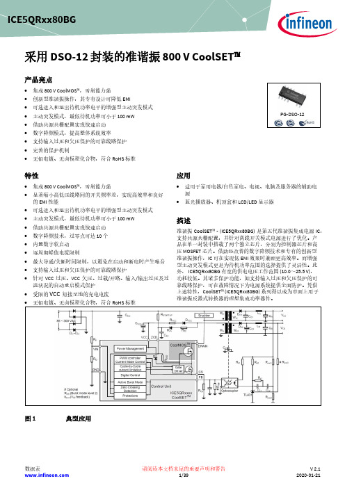
采用 DSO-12 封装的准谐振 800 V CoolSET ™产品亮点• 集成 800 V CoolMOS ™,雪崩能力强 • 创新型准谐振操作,其专有设计可降低 EMI• 可选进入和退出待机功率电平的增强型主动突发模式 • 主动突发模式,最低待机功率可小于 100 mW • 借助共源共栅配置实现快速启动 • 数字降频模式,提高整体系统效率 • 支持输入过压和欠压保护的可靠线路保护 • 完善的保护机制•无铅电镀、无卤模塑化合物,符合 RoHS 标准特性• 集成 800 V CoolMOS ™,雪崩能力强• 显著缩小高低压线路间的开关频率差,实现高效率和良好的 EMI 性能• 可选进入和退出待机功率电平的增强型主动突发模式 • 主动突发模式,最低待机功率可小于 100 mW • 借助共源共栅配置实现快速启动 • 数字降频技术,过零点可达 10 个 • 内置数字软启动 • 逐周期峰值电流限制• 最大导通/关断时间限制,以避免在启动和断电时产生噪音 • 支持输入过压和欠压保护的可靠线路保护•针对 VCC 过压、VCC 欠压、过载/开路、输入/输出过压及过温状况的自动重启模式保护• 受限的 VCC 短接至地的充电电流• 无铅电镀、无卤模塑化合物,符合 RoHS 标准应用• 适用于家用电器/白色家电、电视、电脑及服务器的辅助电源• 蓝光播放器、机顶盒和 LCD/LED 显示器描述准谐振 CoolSET ™ - (ICE5QRxx80BG) 是第五代准谐振集成电源 IC ,支持共源共栅配置,并针对离线开关模式电源进行了优化。
产品在单一封装中搭载了两个独立芯片,分别为控制器芯片和高压 MOSFET 芯片。
借助经改善的数字降频技术和专有的创新型准谐振操作,IC 可在实现低 EMI 效果时兼顾更高效率。
而增强型主动突发模式更是为待机功率范围的选择提供了灵活性。
此外, ICE5QRxx80BG 有宽的供电电压工作范围 (10.0~25.5 V), 功耗较低。