TDA9116中文资料
AD9516_3中文版资料

AD9516_3----集成的2.0 GHz VCO的14路输出时钟发生器一、特征:①低相位噪声,锁相环(PLL)②片上VCO从1.75 GHz到2.25 GHz调谐③外部可选的VCO / VCXO 高达2.4 GHz④1个差分或2个单端参考输入⑤接受LVPECL ,LVDS或CMOS 250 MHz的输出频率⑥6双1.6 GHz的LVPECL输出,每对输出共享1到32位分频器与粗相位延迟⑦4对为800 MHz LVDS时钟输出,每对输出共用两个级联的粗相位延迟1到32的分频器⑧上电时所有输出自动同步可用手动输出同步64引脚LFCSP二、介绍:AD9516 -31集成了片上PLL和VCO,提供了多输出时钟分配功能,具有亚皮秒级的抖动性能。
片上VCO从1.75 GHz到2.25 GHz调谐,芯片外部可以使用高达2.4 GHz的VCO / VCXO 。
AD9516- 3侧重于低抖动和相位噪声数据转换器的性能最大化问题,可以应用于对抖动和相位噪声要求很高的问题上。
三、应用①低抖动,低相位噪声时钟分配②10/40/100 Gb /秒的网络线卡,包括SONET③同步以太网,OTU2/3/4④前向纠错(G.710 )⑤高速时钟的ADCs, DACs, DDSs, DDCs, DUCs, MxFEs⑥高性能无线收发器⑦自动测试设备(ATE)和高性能仪器仪表四、芯片的规格(1)供应的电源:Vs=Vs_LVPECL=3.3 V ± 5%;Vs≤ Vcp≤ 5.25 V; Ta= 25°C; RSET = 4.12 kΩ; CPRSET = 5.1 kΩ四、原理框图AD9516-3具有6个LVPECL输出(三对),4个LVDS输出(两对)。
每个LVDS输出可配置为两个CMOS输出,LVPECL输出工作频率为1.6 GHz ,LVDS输出工作频率为800 MHz,CMOS输出工作频率为250 MHz。
2SA966资料

TOSHIBA Transistor Silicon PNP Epitaxial Type (PCT Process)2SA966Audio Power Amplifier Applications• Complementary to 2SC2236 and 3-W output applications.Absolute Maximum Ratings (Ta = 25°C)Characteristics Symbol Rating UnitCollector-base voltage V CBO −30 V Collector-emitter voltage V CEO −30 V Emitter-base voltage V EBO −5 V Collector current I C−1.5 AEmitter currentI E 1.5 A Collector power dissipation P C 900 mW Junction temperature T j 150 °C Storage temperature rangeT stg−55 to 150°CNote: Using continuously under heavy loads (e.g. the application of high temperature/current/voltage and the significant change in temperature, etc.) may cause this product to decrease in thereliability significantly even if the operating conditions (i.e. operating temperature/current/voltage, etc.) are within the absolute maximum ratings.Please design the appropriate reliability upon reviewing the Toshiba Semiconductor Reliability Handbook (“HandlingPrecautions”/Derating Concept and Methods) and individual reliability data (i.e. reliability test report and estimated failure rate, etc).Unit: mmJEDEC TO-92MOD JEITA ―TOSHIBA 2-5J1A Weight: 0.36 g (typ.)Electrical Characteristics (Ta = 25°C)Characteristics Symbol TestCondition MinTyp.Max UnitCollector cut-off current I CBO V CB = −30 V, I E = 0 ――−100nAEmitter cut-off current I EBO V EB = −5 V, I C = 0 ――−100nA Collector-emitter breakdown voltage V (BR) CEO I C = −10 mA, I B = 0 −30 ―― V Emitter-base breakdown voltage V (BR) EBO I E = −1 mA, I C = 0 −5 ―― VDC current gain h FE(Note)V CE = −2 V, I C = −500 mA 100 ― 320Collector-emitter saturation voltage V CE (sat)I C = −1.5 A, I B = −0.03 A ――−2.0V Base-emitter voltage V BE V CE = −2 V, I C = −500 mA ――−1.0V Transition frequency f T V CE = −2 V, I C = −500 mA ― 120 ― MHz Collector output capacitance C ob V CB = −10 V, I E = 0, f = 1 MHz ― 40 ― pF Note: h FE classification O: 100 to 200, Y: 160 to 320Markinglead (Pb)-free package orlead (Pb)-free finish.indicatorCollector current I C (mA)h FE – ICD C c u r re n t g a i n h F ECollector current I C (mA)V CE (sat) – I CC o l l e c t o r -e m i t t e r s a t u r a t i on v o l t a g eV C E (s a t ) (V )Base-emitter voltage V BE (V)I C – V BEC oll e c t o rc u r r e n t I C (m A )Ambient temperature Ta (°C)P C – TaC o l l e c t o r p owe r d i s s ip a t io n P C (W )Collector-emitter voltage V CE (V)Safe Operating AreaC o l l e c t o r c u r r e n t I C (A )1.00 0 20 40 60 80 100 120 140 160 1800.20.40.60.8−−−−−−−−−−−−−−−−−−Collector-emitter voltage V CE (V)I C – V CEC o l l e c t o r c u r r e n t I C (m A )−−−−−−−−−−−−−−−−−RESTRICTIONS ON PRODUCT USE20070701-EN •The information contained herein is subject to change without notice.•TOSHIBA is continually working to improve the quality and reliability of its products. Nevertheless, semiconductor devices in general can malfunction or fail due to their inherent electrical sensitivity and vulnerability to physical stress. It is the responsibility of the buyer, when utilizing TOSHIBA products, to comply with the standards of safety in making a safe design for the entire system, and to avoid situations in which a malfunction or failure of such TOSHIBA products could cause loss of human life, bodily injury or damage to property.In developing your designs, please ensure that TOSHIBA products are used within specified operating ranges as set forth in the most recent TOSHIBA products specifications. Also, please keep in mind the precautions and conditions set forth in the “Handling Guide for Semiconductor Devices,” or “TOSHIBA Semiconductor Reliability Handbook” etc.• The TOSHIBA products listed in this document are intended for usage in general electronics applications (computer, personal equipment, office equipment, measuring equipment, industrial robotics, domestic appliances, etc.).These TOSHIBA products are neither intended nor warranted for usage in equipment that requires extraordinarily high quality and/or reliability or a malfunction or failure of which may cause loss of human life or bodily injury (“Unintended Usage”). Unintended Usage include atomic energy control instruments, airplane or spaceship instruments, transportation instruments, traffic signal instruments, combustion control instruments, medical instruments, all types of safety devices, etc.. Unintended Usage of TOSHIBA products listed in his document shall be made at the customer’s own risk.•The products described in this document shall not be used or embedded to any downstream products of which manufacture, use and/or sale are prohibited under any applicable laws and regulations.• The information contained herein is presented only as a guide for the applications of our products. No responsibility is assumed by TOSHIBA for any infringements of patents or other rights of the third parties which may result from its use. No license is granted by implication or otherwise under any patents or other rights of TOSHIBA or the third parties.• Please contact your sales representative for product-by-product details in this document regarding RoHS compatibility. Please use these products in this document in compliance with all applicable laws and regulations that regulate the inclusion or use of controlled substances. Toshiba assumes no liability for damage or losses occurring as a result of noncompliance with applicable laws and regulations.。
9906;中文规格书,Datasheet资料
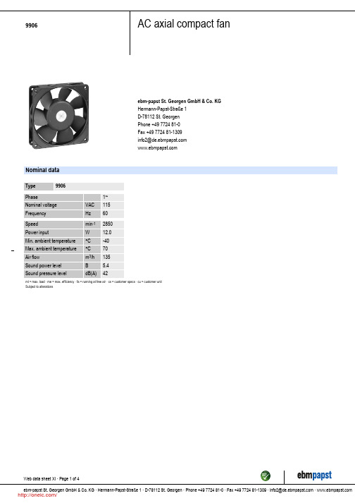
Nominal data
Type Phase Nominal voltage Frequency Speed Power input Min. ambient temperature Max. ambient temperature Air flow Sound power level Sound pressure level VAC Hz min-1 W °C °C m3/h B dB(A) 9906 1~ 115 60 2850 12.0 -40 70 135 5.4 42
/
9906
AC axial compact fan
Technical features
General description AC voltage fan with internal rotor shaded-pole motor. Protected from overload by impedance protection. Fan housing made of metal, impeller made of mineral-reinforced PA plastic. Air exhaust over bars. Direction of rotation counter-clockwise seen on rotor. Electrical connection to 2 flat plugs 2.8 x 0.5 mm. Fan housing with grounding lug for M4 tapping screw. Mass 320 g. Please note our new ACmaxx series. With identical fastening dimensions and voltages, this series achieves higher energy efficiency. 0.325 kg 119 x 119 x 25 mm Mineral-reinforced PA plastic Metal Air exhaust over bars Left, looking at rotor Ball bearings 52500 h 25000 h 2 flat plugs 2.8 x 0.5 mm Protected from overload using impedance protection VDE, CSA, UL, CE
TDA21106资料

Number Name Description1 GATE HS Gate drive output for the N-Channel High side MOSFET2 BOOT Floating bootstrap pin. To beconnected to the external bootstrapcapacitor to generate the gate drive voltage for the high side N-ChannelMOSFET 3 PWM Input for the PWM controller signal 4 GND Ground 5 GATE LS Gate drive output for the N-Channel Low Side MOSFET 6 VCC Supply voltage 7 PVCC Input to adjust the High Side gatedrive8 PHASE To be connected to the junction ofthe High Side and the Low Side MOSFET • Fast rise and fall times for frequencies up to 2 MHz• Capable of sinking more than 4A peak currents for lowest switching losses• Charges High Side MOSFET gate drive voltage from 6 to 12V according to PVCC setting; Low Side MOSFET at 12 V.• Adjustable High Side MOSFET gate drive voltage via PVCC pin for optimizing ON losses and gate drive losses• Integrates the bootstrap diode for reducing the part count• Prevents from cross-conducting by adaptive gate drive control • High voltage rating on Phase node• Supports shut-down mode for very low quiescent current through three-state input • Compatible to standard PWM controller ICs (Intersil, Analog Devices) • Floating High Side MOSFET drive• Footprint compatible to TDA21101G and HIP6601B• Ideal for multi-phase Desktop CPU supplies on motherboards and VRM´sType Package Marking Ordering Code TDA21106 P-DSO-8 21106 Q67042-S4223GATE PHASE2 7 P VCC3 6 V CCGND GATE LSP-DSO-8High speed Driver with bootstrapping for dual Power MOSFETsFeaturesPinoutGeneral DescriptionThe dual high speed driver is designed to drive a wide range of N-Channel low side and N-Channel high side MOSFETs with varying gate charges. It has a small propagation delay from input to output, short rise and fall times and the same pin configuration to be compatible to TDA21101G and HIP6601B. In addition it provides protection features as well as a three-state mode for efficiency reasons. The high breakdown voltage makes it suitable for mobile applications.Target applicationThe dual high speed driver is designed to work well in half-bridge type circuits where dual N-Channel MOSFETs are utilized. A circuit designer can fully take advantage of the driver´s capabilities in high-efficiency, high-density synchronous DC/DC converters that operate at high switching frequencies, e.g. in multi-phase convertersfor CPU supplies on motherboards and VRM´s but also in motor drive and class-D amplifier type applications.Absolute Maximum RatingsAt Tj = 25 °C, unless otherwise specifiedValue Parameter SymbolMin. Max.UnitVoltage supplied to ‘VCC’ pin; DC V VCC -0.3 25 Voltage supplied to ‘PVCC’ pin; DC V PVCC -0.3 25 Voltage supplied to ‘PWM’ pin V PWM -0.3 5,5 Voltage supplied to ‘BOOT’ pin referenced to ‘PHASE’ V BOOT –V PHASE-0,3 25 Voltage supplied to ‘BOOT’ pin referenced to ‘GND’ V BOOT-0,3 45 Voltage rating at ‘PHASE’ pin, DC V PHASE -1 25 Voltage rating at ‘PHASE’ pin, t pulse_max = 500nsMax Duty Cycle = 2%V PHASE -20 30Voltage supplied to GATE HS pin referenced to ‘PHASE’ T pulse_max < 100ns, E nergy < 2uJ V GATEHS -3.5 V BOOT+0.3Voltage supplied to GATE LS pin referenced to ‘GND’ T pulse_max < 100ns, E nergy < 2uJ V GATELS -5 V VCC+0.3VJunction temperature T J -25 150 Storage temperature T S -55 150°C ESD Rating; Human Body Model 4 KV IEC climatic category; DIN EN 60068-1 55/150/56 -Thermal CharacteristicValuesParameter SymbolMin.Typ. Max.UnitThermal resistance, junction-soldering point 95Thermal resistance, junction-ambient 125K/WOperating ConditionsAt Tj = 25 °C, unless otherwise specifiedValuesParameter Symbol ConditionsMin.Typ. Max.UnitVoltage supplied to‘VCC’ pinsV VCC10.813.2VVoltage supplied to ‘PVCC’ pins V PVCC 613.2VInput signal transitionfrequencyf 0.1 2 MHzPower dissipation P TOT T A = 25 °C, T J = 125 °C 0.8 W Junction temperature T J-25 150 °C Electrical CharacteristicAt Tj = 25 °C, unless otherwise specifiedValues Parameter SymbolConditionsMin. Typ. Max.UnitSupply CharacteristicQuiescent current I PVCC+I VCCQ 1.8 V ≤ V PWM≤ 3.0 V 1,3. 3 VCC supply current I VCC f =1 MHz,V PVCC = V VCC = 12 VNo load5 8 PVCC supply current I PVCC f =1 MHz,V PVCC = V VCC = 12 VNo load 6 8.5mAUnder-voltagelockoutV VCC rising threshold 9.7 10.1 10.5Under-voltage lockout V VCC fallingthreshold 7.3 7.6 8.0VInput CharacteristicCurrent in ‘PWM’ pin I PWM_L V_PWM = 0.4 V -80 -115 -150 Current in ‘PWM’ pin I PWM_H V_PWM = 4.5 V 120 180 250µAShut down window V IN_SHUT t_SHUT > 300 ns 1.7 3.1 V Shut down hold-offtimet_SHUT 1.6 V ≤ V PWM≤ 3.2 V100 190 300 ns PWM pin open V PWM_O 1.8 2.0 2.2 PWM Low level V PWM_L 1.4 PWM High level V PWM_H 3.7 VPulse width High Side t_P= Pulse width on PWMpin40 nsAt Tj = 25 °C, unless otherwise specifiedDynamic CharacteristicTurn-on propagation Delay High Side t d(ON)_HS 20 35 Turn-off propagation delay High Side t d(OFF)_HS 1525Rise time High Side t r_HS 20 33 Fall time High Side t f_HS 15 25 Turn-on propagation Delay Low Sidet d(ON)_LS 15 27 Turn-off propagation delay Low Sidet d(OFF)_LS 10 20 Rise time Low Side t r_LS 20 33Fall time Low Side t f_LSP PVCC = V VCC = 12 V C ISS = 3000 pF 15 25 nsAt Tj = 125 °C, unless otherwise specifiedDynamic CharacteristicTurn-on propagation Delay High Side t d(ON)_HS 25 Turn-off propagation delay High Sidet d(OFF)_HS18Rise time High Side t r_HS24 Fall time High Side t f_HS 22 Turn-on propagation Delay Low Sidet d(ON)_LS 18 Turn-off propagation delay Low Sidet d(OFF)_LS15 Rise time Low Side t r_LS 21 Fall time Low Side t f_LSP PVCC = V VCC = 12 V C ISS = 3000 pF19nsTiming diagramAt Tj = 25 °C, unless otherwise specifiedValuesParameter Conditions Min.Typ. Max.Unit Output Characteristic High Side (HS) and Low Side (LS), ensured by design HS; Source V PVCC = V VCC = 12 V I _HS_SRC = 2 A 1 (1)ΩHS; Sink V PVCC = V VCC = 12 V 0.9 1.3 Ω LS; Source V PVCC = V VCC = 12 V I _HS_SRC = 2 A 1.4 (2)ΩOutput Resistance LS; Sink V PVCC = V VCC = 12 V 0.9 1.3 ΩHS; Source 4HS; Sink 4LS; Source 4Peak output-current LS; Sink V PVCC = V VCC = 12 V t_P_HS / Pulse < 20 ns t_P_LS / Pulse < 40 ns 4A 1Incremental resistance V BOOT -V GATEHS =4.3V @ I SOURCE =2A 2Incremental resistance V VCC –V GATELS =4.4V @ I SOURCE =2A1 V ~5V1 Vt f LSt r LSPackage Drawing P-DSO-8-3Footprint Drawing P-DSO-8-3e A L B1,27 mm 5,69 mm 1,31 mm 0,65 mmPublished byInfineon Technologies AG,Bereichs KommunikationSt.-Martin-Strasse 53,D-81541 MünchenInfineon Technologies AG 1999All Rights Reserved.Attention please!The information herein is given to describe certain components and shall not be considered as warranted characteristics.Terms of delivery and rights to technical change reserved.We hereby disclaim any and all warranties, including but not limited to warranties of non-infringement, regarding circuits, descriptions and charts stated herein.Infineon Technologies is an approved CECC manufacturer.InformationFor further information on technology, delivery terms and conditions and prices please contact your nearest Infineon Technologies Office in Germany or our Infineon Technologies Representatives worldwide (see address list).WarningsDue to technical requirements components may contain dangerous substances.For information on the types in question please contact your nearest Infineon Technologies Office. Infineon Technologies Components may only be used in life-support devices or systems with the express written approval of Infineon Technologies, if a failure of such components can reasonably be expected to cause the failure of that life-support device or system, or to affect the safety or effectiveness of that device or system Life support devices or systems are intended to be implanted in the human body, or to support and/or maintain and sustain and/or protect human life. If they fail, it is reasonable to assume that the health of the user or other persons may be endangered.。
LM5116中文手册(DOC)
LM5116宽范围同步降压控制器概述该LM5116是一个同步降压控制器,适用于高输入电压或宽输入电压的环境中。
其控制方式是电流模式控制,该控制方式是利用一个模拟出来的电流斜坡。
电流模式控制提供了固有的线路前馈,以周期电流限制和易于循环的环路补偿。
电流模式控制提供固有的线性前馈,周期性循环的电流限制以及环路补偿。
仿真控制斜坡的使用可以减少脉宽调制电路的噪声灵敏度,是高输入电压应用中实现小占空比的可靠控制所必需的。
其工作频率可编程,从50kHz 至1MHz。
LM5116是驱动外部高边和低边的NMOS电源开关,这两个MOS管有自适应的死区时间控制。
可由用户选择二极管仿真的模式使芯片在轻负载时能够提高不连续工作模式的效率。
低静态关断电流就能使芯片不工作,并消耗总输入电流中的10μA。
其它特点包括一个高压偏置调节器、能自动切换到外部偏置以提高效率、热关断、频率同步、周期性限流、以及自适应线性欠压锁定。
该芯片选用TSSOP-20的封装,具有一个额外的焊盘以增加散热,这种封装方式在大功率模式下是十分有效的。
特色仿峰值电流模式输入电压范围可达100V低关断电流能驱动标准或逻辑级的MOS管栅极驱动电流可高达3.5A自由运行或同步操作到1MHz可选择的二极管仿真模式输出电压范围1.215V——80V电压基准精度为1.5%可编程限流可编程软启动可编程的线性欠压锁定自动切换到外部偏置电压TSSOP-20EP裸露焊盘热关断典型电路引脚名称描述1 VIN 芯片电源电压,输入电压2 UVLO 如果UVLO引脚的电压低于1.215V,调节器会进入待机模式(VCC调节器工作,开关驱动电路不工作)。
如果UVLO引脚电压高于1.215V,这个调节器正常工作。
可以通过外部分压器来设置欠压关断的阈值。
当EN引脚为高时,这个引脚存在一个固定的5μA上拉电流。
在工作在电流限制模式时,UVLO会每隔256个时钟周期被拉到地。
3 RT/SYNC 内部晶振可以通过一个该引脚和地之间的电阻来设置。
AD9116中文资料

元器件交易网
AD9114/AD9115/AD9116/AD9117
TABLE OF CONTENTS
Features .............................................................................................. 1 Applications....................................................................................... 1 General Description ......................................................................... 1 Product Highlights ........................................................................... 1 Revision History ............................................................................... 2 Functional Block Diagram .............................................................. 3 Specifications..................................................................................... 4
2. CMOS Clock Input. High speed, single-ended CMOS clock input supports 125 MSPS conversion rate.
元器件的替换资料

元器件的替换资料1.健伍激光头KCP1H的代换经过在长虹VD9000型VCD机上试⽤,索尼KSS-213激光头直接代换健伍KCP1H激光头,代换后装⼊碟⽚试机⼀切正常,以前不能读的碟⽚都能很快读出,⽽且播放效果良好。
2.长虹R2118AE彩电中周ST6019的代⽤中周ST6019可⽤TC31157和TRF1162T代换。
3.29英⼨⾼清⾏输出管在代⽤时的注意事项因为100Hz彩电⾏频是普通机型的2倍,对⾏输出管的⼯作频率要求⾼,除了要满⾜普通彩电的条件外,还须考虑其下降时间是普通彩电⾏输出管的tf=lIxs左右,⽽100Hz彩电的⾏榆出管则要求其tf⼩于O.6µs。
4.应⽤于电磁炉(灶)绝缘栅双极晶体管(IGBT)的参数要求应⽤于电磁炉(灶)的IGBT管应选取BVceo≥1000V、ICm≥7A、PCM≥100W、β≥40的。
才能保证其在电路上胜任。
5.三洋系列机芯彩电4.43M晶振的代换三洋系列机芯彩电中的UPC1423、LA7685、LA7688、LA76810集成电路,晶振均为4.43MHz,损坏后出现的故障多种多样,市⾯上所售⼀般的4.43M晶振均⽆法直接更换,经摸索发现,只要在晶振引脚上串接⼀个10-18P的电容,⼏乎都能代换成功。
6.康佳F953DB彩电中周的代换康佳F953DB彩电中周型号为2703119,可以⽤1445、7851、丽恒703025类似功能的中周代⽤。
7.嘉华25S5彩电CPU的代换DMC73C167-004(英⽂菜单)代换DMC73C16-003(中⽂菜单)⽅法,将DMC73C167-004第28,29脚去掉,按脚位顺序装上即可。
8.关于IIC总线彩电微处理器的代换原则由于IIC总线彩电微处理器是⼀个数字电路系统,它的⼯作状态或功能是由存储的数据所决定的。
所以它的代⽤就不同于模拟电路的集成电路,只是脚功能相同、⼯作环境和条件相同就可以代换。
原则上以原型号(连后缀也要相同)代换,也可以⽤引脚功能相同的其他型号代换,但需要同时更换配套的存储器数据。
96256芯片手册

96256芯片手册一、概述96256芯片是一款高性能的16位随机数生成器芯片,具有低功耗、高精度、高可靠性等特点。
该芯片广泛应用于各种需要随机数的应用领域,如加密解密、密码学、测试测量等。
二、芯片结构96256芯片主要由以下几个部分组成:1. 核心电路:芯片的核心是一个高性能的16位随机数生成器,能够产生高质量的随机数。
2. 控制电路:芯片具有灵活的控制接口,可以通过外部控制信号进行配置和调整。
3. 寄存器:芯片内部有一些可配置的寄存器,用于存储和控制随机数的生成过程。
4. 电源电路:芯片采用低功耗设计,内置电源电路,可以提供稳定的电源输出。
三、引脚定义96256芯片的引脚定义如下:1. VCC:芯片供电端,接正电压。
2. GND:接地端。
3. OUT:输出端,连接外部设备需要随机数的接口。
4. CLK:时钟输入端,用于控制随机数的生成速度。
5. CTRL:控制输入端,用于配置和调整芯片的工作状态。
四、应用示例以下是一个简单的应用示例:1. 硬件连接:将96256芯片与需要随机数的设备连接起来,通过OUT接口传输随机数。
2. 软件配置:通过控制输入端CTRL,配置芯片的工作状态,如设置随机数的生成速度、精度等。
3. 程序调用:在需要随机数的程序中,调用96256芯片的OUT接口,获取所需的随机数。
五、注意事项1. 确保芯片供电电压稳定,避免过高或过低的电压导致芯片损坏。
2. 根据需要调整控制输入端CTRL的信号,确保芯片正常工作。
3. 避免在时钟输入端CLK上加过大的负载,以免影响随机数的生成质量。
4. 长时间不使用的芯片,建议定期进行放电操作,以保持芯片的良好性能。
六、维护保养1. 定期检查芯片的工作状态,如发现异常,及时进行检修。
2. 如需更换损坏的芯片,请使用原型号的芯片,以保证良好的性能和可靠性。
- 1、下载文档前请自行甄别文档内容的完整性,平台不提供额外的编辑、内容补充、找答案等附加服务。
- 2、"仅部分预览"的文档,不可在线预览部分如存在完整性等问题,可反馈申请退款(可完整预览的文档不适用该条件!)。
- 3、如文档侵犯您的权益,请联系客服反馈,我们会尽快为您处理(人工客服工作时间:9:00-18:30)。
cancellation and moiré cancellation output
Vertical section s 200 Hz maximum frequency s Vertical ramp for DC-coupled output staeans of tracking system
DC/DC controller section
s Step-up and step-down conversion modes s External sawtooth configuration s Bus-controlled output voltage s Synchronization on hor. frequency with phase
adjustments of: C-correction, S-correction for super-flat CRT, Vertical size, Vertical position s Vertical moiré cancellation through vertical ramp waveform s Compensation of vertical breathing with EHT variation
selection s Selectable polarity of drive signal
DESCRIPTION
The TDA9116 is a monolithic integrated circuit assembled in a 32-pin shrink dual-in-line plastic package. This IC controls all the functions related to horizontal and vertical deflection in multimode or multi-frequency computer display monitors.
ORDERING INFORMATION
Ordering code TDA9116
Package Shrink 32 (plastic)
Version 4.0
1/47
1
元器件交易网
Table of Contents
1 - GLOSSARY . . . . . . . . . . . . . . . . . . . . . . . . . . . . . . . . . . . . . . . . . . . . . . . . . . . . . . . . . . . . . . . . . 4 2 - PIN CONFIGURATION . . . . . . . . . . . . . . . . . . . . . . . . . . . . . . . . . . . . . . . . . . . . . . . . . . . . . . . . 5 3 - BLOCK DIAGRAM . . . . . . . . . . . . . . . . . . . . . . . . . . . . . . . . . . . . . . . . . . . . . . . . . . . . . . . . . . . 6 4 - PIN FUNCTION REFERENCE . . . . . . . . . . . . . . . . . . . . . . . . . . . . . . . . . . . . . . . . . . . . . . . . . . 7 5 - QUICK REFERENCE DATA . . . . . . . . . . . . . . . . . . . . . . . . . . . . . . . . . . . . . . . . . . . . . . . . . . . . 8 6 - ABSOLUTE MAXIMUM RATINGS . . . . . . . . . . . . . . . . . . . . . . . . . . . . . . . . . . . . . . . . . . . . . . . 9 7 - ELECTRICAL PARAMETERS AND OPERATING CONDITIONS . . . . . . . . . . . . . . . . . . . . . . 10
Combined with other ST components dedicated for CRT monitors (microcontroller, video preamplifier, video amplifier, OSD controller) the TDA9116 allows fully I2C bus-controlled computer display monitors to be built with a reduced number of external components.
position and adaptation to frequency s Compensation of horizontal breathing through
EW waveform
September 2003
Dynamic correction section
s Output with vertical dynamic correction waveform for dynamic corrections like focus, brightness uniformity, ...
Horizontal section s 150 kHz maximum frequency s Corrections of geometric asymmetry:
Pin cushion asymmetry, Parallelogram s Tracking of asymmetry corrections with vertical
The internal sync processor, combined with the powerful geometry correction block, makes the TDA9116 suitable for very high performance monitors, using few external components.
7.1 - THERMAL DATA . . . . . . . . . . . . . . . . . . . . . . . . . . . . . . . . . . . . . . . . . . . . . . . . . . . . . . . . 10 7.2 - SUPPLY AND REFERENCE VOLTAGES . . . . . . . . . . . . . . . . . . . . . . . . . . . . . . . . . . . . . 10 7.3 - SYNCHRONIZATION INPUTS . . . . . . . . . . . . . . . . . . . . . . . . . . . . . . . . . . . . . . . . . . . . . 10 7.4 - HORIZONTAL SECTION . . . . . . . . . . . . . . . . . . . . . . . . . . . . . . . . . . . . . . . . . . . . . . . . . . 11 7.5 - VERTICAL SECTION . . . . . . . . . . . . . . . . . . . . . . . . . . . . . . . . . . . . . . . . . . . . . . . . . . . . . 12 7.6 - EW DRIVE SECTION . . . . . . . . . . . . . . . . . . . . . . . . . . . . . . . . . . . . . . . . . . . . . . . . . . . . 14 7.7 - DYNAMIC CORRECTION OUTPUT SECTION . . . . . . . . . . . . . . . . . . . . . . . . . . . . . . . . . 15 7.8 - DC/DC CONTROLLER SECTION . . . . . . . . . . . . . . . . . . . . . . . . . . . . . . . . . . . . . . . . . . . 16 7.9 - MISCELLANEOUS . . . . . . . . . . . . . . . . . . . . . . . . . . . . . . . . . . . . . . . . . . . . . . . . . . . . . . . 17 8 - TYPICAL OUTPUT WAVEFORMS . . . . . . . . . . . . . . . . . . . . . . . . . . . . . . . . . . . . . . . . . . . . . . 19 9 - I2C BUS CONTROL REGISTER MAP . . . . . . . . . . . . . . . . . . . . . . . . . . . . . . . . . . . . . . . . . . . 22 10 - OPERATING DESCRIPTION . . . . . . . . . . . . . . . . . . . . . . . . . . . . . . . . . . . . . . . . . . . . . . . . . 26 10.1 -SUPPLY AND CONTROL . . . . . . . . . . . . . . . . . . . . . . . . . . . . . . . . . . . . . . . . . . . . . . . . 26