IS93C46B-3GI中文资料
93LC46

无
128 x 16 位
无
I, E P, SN, ST, MS, OT, MC
93LC56C
2
2.5-5.5
有
可选 x8 或 x16
无
I, E P, SN, ST, MS, MC
93C56A
2
4.5-5.5
无
256 x 8 位
无
I, E P, SN, ST, MS, OT, MC
93C56B
2
4.5-5.5
2048 x 8 位 1024 x 16 位 可选 x8 或 x16 2048 x 8 位 1024 x 16 位 可选 x8 或 x16 2048 x 8 位 1024 x 16 位 可选 x8 或 x16
PE 引脚 温度范围
封装
无
I
OT
无
I
OT
有
I
P, SN, ST, MS, MC
无
I, E OT
架构 (字)
PE 引脚 温度范围
封装
93XX46A/B/C
93AA46A
1
1.8-5.5
无
128 x 8 位
无
I
P, SN, ST, MS, OT, MC
93AA46B
1
1.8-5.5
无
64 x 16 位
无
I
P, SN, ST, MS, OT, MC
93AA46C
1
1.8-5.5
有
可选 x8 或 x16
64 x 16 位
无
I, E P, SN, ST, MS, OT, MC
93LC46CX
1
2.5-5.5
有
可选 x8 或 x16
gc0403 规格书

gc0403 规格书英文回答:The GC0403 is a 1/4-inch CMOS digital image sensor witha resolution of 1280 x 1024 pixels. It has a sensitivity of1.0 V/lux-sec and a dynamic range of 70 dB. The GC0403 is available in a variety of package options, including LGA, QFN, and CSP.Here are some of the key features of the GC0403:1/4-inch CMOS digital image sensor.Resolution: 1280 x 1024 pixels.Sensitivity: 1.0 V/lux-sec.Dynamic range: 70 dB.Available in a variety of package options.The GC0403 is a versatile image sensor that can be used in a variety of applications, including:Security cameras.Surveillance cameras.Automotive cameras.Medical imaging.Industrial inspection.中文回答:GC0403 是一款 1/4 英寸 CMOS 数码图像传感器,分辨率为1280 x 1024 像素。
它的灵敏度为 1.0 V/lux-sec,动态范围为 70 dB。
GC0403 有多种封装选项,包括 LGA、QFN 和 CSP。
以下是 GC0403 的一些主要特性:1/4 英寸 CMOS 数码图像传感器。
中九机顶盒各种机型机芯IC大全供大家分享(刷机必备)

吉祥2009 3晶 14芯
IC:GX3001+GX1121+RDK5812
ABS-S LX-3688A 单晶12芯
IC:GX3001+GX1121+5812
集信科技V6 3晶9芯
IC:1108EG(Hi3121)+HI2023+5812
集信科技 V4.V6 2晶9芯 B型
IC:0001+HN4F74+5812
集信科技 V4.V6 A型
IC:AVL1108EG+HTV903F+M88TS2000
--------------------------------------------------------------------------------
-- 作者:adok
IC:HTV903+AVL1108+RDA5812_
幸运之星YJ5988 2晶 10芯
IC:HTV903F+AVL1108EGa+AV2020
克莱尔HT701 1晶10芯
村村通ZL-5188B 2晶13芯
IC:HTV903+AVL1108+RDK5812
村村通ZL-5188B 2晶10芯
IC:HTV903+AVL1108EGA+5812
村村通ZL5188B 1晶13芯
村村通 2晶6芯
IC:HN4+0001+5812
村村通ZL-5188A 2晶11芯
IC:HTV903+AVL1108+RDK5812
村村通ZL-6188C 10芯
IC:GX3001+GX1121+RDK5812
博世柴油电喷资料

标准 型
玉柴电控知识应知应会培训系列教材 DS-NF/EAN
CRIN2喷油器
回油孔 进油孔
电接 口
标识
回油 孔
进油孔
内 部 参 考 结 构
最大喷油压力:1600 bar 喷嘴:mini-sac-hole 玉柴电控知识应知应会培训系列教材
22
CRIN2工作原理
喷嘴置位
回油 线圈 衔铁 球阀
的共轨压力指令由高压供
其它传感 器输入
油泵控制
共轨压力是闭环控制
玉柴电控知识应知应会培训系列教材
5
博世共轨系统在6J系列发动机的布置示例
增压压力 传感器 喷油器电磁 阀驱动线
共轨油压 传感器
整车功能端 高压泵 油量计量阀
ECU
发动机功能端
玉柴电控知识应知应会培训发动机的布置示例
接插件引脚 1 2
引脚定义 电源(+) 控制信号
玉柴电控知识应知应会培训系列教材
36
喷油器电磁阀
高速强力电磁阀 工作电压:24V 提升电压: UBoost =48 V 工作电流:提升电流:IBoost =25±1 A 保持电流:IHold =12±1 A 线圈静态电阻:230 mΩ 电磁阀开启时间:110±10 μs 电磁阀关闭时间:30±5 μs 集成在喷油器体内
K线(ISO K-Line) 用于故障诊断和整车标定
玉柴电控知识应知应会培训系列教材
35
燃油计量阀(MeUN)执行器
比例电磁阀 PWM控制(165~195Hz) 线圈电阻:2.6~3.15欧姆 最大工作电流:1.8A 集成安装在高压油泵上,不允许随便拆卸
ECU引脚 3.09 3.10
赛米控丹佛斯电子 SEMiX604GB176HDs 数据表

SEMiX ®4sTrench IGBT ModulesSEMiX604GB176HDsFeatures•Homogeneous Si•Trench = Trenchgate technology •V CE(sat) with positive temperature coefficient•UL recognised file no. E63532Typical Applications*•AC inverter drives •UPS•Electronic weldersAbsolute Maximum Ratings SymbolConditions Values UnitIGBT V CES 1700V I C T j =150°CT c =25°C 567A T c =80°C402A I Cnom 400A I CRMI CRM = 2xI Cnom 800A V GES -20...20V t psc V CC =1000V V GE ≤ 20V V CES ≤ 1700VT j =125°C10µs T j-55...150°C Inverse diode I F T j =150°CT c =25°C 740A T c =80°C 496A I Fnom400A I FRM I FRM = 2xI Fnom800A I FSM t p =10ms, sin 180°, T j =25°C2700A T j -40 (150)°C Module I t(RMS)T terminal =80°C600A T stg -40...125°C V isolAC sinus 50Hz, t =1min4000VCharacteristics SymbolConditions min.typ.max.UnitIGBT V CE(sat)I C =400A V GE =15V chiplevelT j =25°C 2 2.45V T j =125°C 2.5 2.9V V CE0T j =25°C 1 1.2V T j =125°C0.9 1.1V r CE V GE =15VT j =25°C 2.5 3.1m ΩT j =125°C3.94.5m ΩV GE(th)V GE =V CE , I C =16mA5.25.86.4V I CES V GE =0V V CE =1700V T j =25°C 0.124mA T j =125°C mA C ies V CE =25V V GE =0Vf =1MHz 35.3nF C oes f =1MHz 1.46nF C res f =1MHz1.17nF Q G V GE =- 8 V...+ 15 V 3732nC R Gint T j =25°C 1.88Ωt d(on)V CC =1200V I C =400A V GE =±15V R G on =3ΩR G off =3ΩT j =125°C 360ns t r T j =125°C 65ns E on T j =125°C 215mJ t d(off)T j =125°C 900ns t f T j =125°C 165ns E off T j =125°C165mJ R th(j-c)per IGBT 0.058K/WCharacteristics SymbolConditionsmin.typ.max.UnitInverse diodeV F = V EC I F =400AV GE =0V chipT j =25°C 1.5 1.70V T j =125°C 1.4 1.6V V F0T j =25°C 0.9 1.1 1.3V T j =125°C0.70.9 1.1V r FT j =25°C 1.0 1.0 1.0m ΩT j =125°C1.31.3 1.3m ΩI RRM I F =400A di/dt off =6600A/µs V GE =-15VV CC =1200VT j =125°C 560A Q rr T j=125°C131µC E rr T j =125°C 95mJR th(j-c)per diode0.081K/WModule L CE 22nH R CC'+EE'res., terminal-chip T C =25°C 0.7m ΩT C =125°C1m ΩR th(c-s)per module 0.03K/W M s to heat sink (M5)35Nm M tto terminals (M6)2.55Nm Nmw400gTemperatur Sensor R 100T c =100°C (R 25=5 k Ω)493 ± 5%ΩB 100/125R (T)=R 100exp[B 100/125(1/T-1/T 100)]; T[K];3550 ±2%K SEMiX ® 4sTrench IGBT ModulesSEMiX604GB176HDsFeatures•Homogeneous Si•Trench = Trenchgate technology •V CE(sat) with positive temperature coefficient•UL recognised file no. E63532Typical Applications*•AC inverter drives •UPS•Electronic weldersFig. 1: Typ. output characteristic, inclusive R CC'+ EE'Fig. 2: Rated current vs. temperature I C = f (T C )Fig. 3: Typ. turn-on /-off energy = f (I C )Fig. 4: Typ. turn-on /-off energy = f (R G )Fig. 5: Typ. transfer characteristic Fig. 6: Typ. gate charge characteristicFig. 7: Typ. switching times vs. I C Fig. 8: Typ. switching times vs. gate resistor R GFig. 9: Typ. transient thermal impedance Fig. 10: Typ. CAL diode forward charact., incl. R CC'+EE'Fig. 11: Typ. CAL diode peak reverse recovery current Fig. 12: Typ. CAL diode recovery chargeThis is an electrostatic discharge sensitive device (ESDS), international standard IEC 60747-1, Chapter IX* The specifications of our components may not be considered as an assurance of component characteristics. Components have to be tested for the respective application. Adjustments may be necessary. The use of SEMIKRON products in life support appliances and systems is subject to prior specification and written approval by SEMIKRON. We therefore strongly recommend prior consultation of our staff.spring configuration。
施耐德电气 ProTech-GII 三冗余过速保护装置 (03370-J) 产品规格书说明书

®Product Specification 03370(RevisionJ, 11/2022)ProTech ‐GIIOverspeed Protection Device(Triple Modular Redundant)DescriptionThe ProTech-GII is an overspeed safety device designed to safely shut down steam, gas, and hydro turbines of all sizes upon sensing an overspeed or over-acceleration event. This device accurately monitors turbine rotor speed and acceleration via active or passive magnetic pickups (MPUs) and issues ashutdown command to the turbine’s trip valve(s) or corresponding trip system. Depending on the system design, the ProTech-GII can be purchased with two dual-redundant trip relay outputs using a 2-out-of-3 voted architecture, or with three independent non-voted trip relay outputs. Individual alarm relays, 4–20 mA speed readouts, and Modbus ® * communications make this overspeed device easy to integrate into any turbine safety system.*—Modbus is a trademark of Schneider Automation Inc.The ProTech-GII is available in flush-mount models designed to be installed within a standard 24” (610 mm) cabinet front door, or models designed to be bulkhead mounted on a wall or skid near the turbine set. Designed for harsh environments when installed within an enclosure, this device has an ingress protection rating of IP56 (protected against dust and completely protected against jets of water of similar force to heavy seas).Designed for high reliability, each ProTech-GII module (A, B, C), depending on the purchased model, accepts two high-voltage power inputs (90–240 Vac / 100–150 Vdc) or one high-voltage power input (90–240 Vac / 100–150 Vdc) and one low-voltage power input (18–32 Vdc). This design works on a high-signal-select basis, allowing the unit to fully operate with either or both power sources available.ApplicationsThe ProTech-GII is designed to safely shut down steam, gas, and hydro turbines upon sensing a turbine overspeed or over-acceleration event. The device’s 12 millisecond response time and 0.5 to 80 000 rpm speed range make it ideal for application on all types and sizes of turbines.∙ IEC61508 SIL-3Certified ∙ API670 & API612Compliant ∙ 2-out-of-3 voting ∙ High availability(TMR) ∙ Accelerationprotection ∙ On-line testing ∙ On-line repair ∙ Overspeed tripand test logs ∙ Modbuscommunications ∙ Password securityprotection ∙ 12 millisecondresponse time (independent voted output models) ∙ Internal frequencygenerator ∙ Optional Ethernetcommunication gatewayReleasedThe ProTech-GII models with two dual-redundant relay outputs are design to be applied with simplex or dual-redundant trip block assemblies or trip systems. The ProTech-GII models with three independent non-voted output models are designed to be applied with special turbine trip block assemblies that perform the 2-out-of-3 voting within their design.This fast acting overspeed protection device is designed to be applied in conjunction with a turbine control or trip system to safely shut down the turbine. Interface with related control systems or plant Distributed Control Systems (DCSs) can be performed via the ProTech-GII’s redundant hard-wired input and output signals or through its triple-redundant serial Modbus communications ports. Optionally, Ethernet gateways can be purchased to easily interface with plant Ethernet networks.Certified as an IEC61508 SIL-3 (Safety Integrity Level Three) safety device, the ProTech-GII can easily be applied within an IEC61508 or IEC61511 based safety system. A thorough product manual is provided to instruct users on how to apply the ProTech-GII to meet IEC based requirements.Designed for system-critical applications, the ProTech-GII’s triple-modular architecture coupled with its on-line testing and on-line repair capabilities give it one of the highest availability and reliability ratings in the industry. FunctionalityOn-line Testing—Each ProTech-GII module can be tested manually from the module’s front panel, Modbus communications port, or automatically via its auto-test routine function. The ProTech-GII allows users to configure an overspeed test to be performed automatically on a periodic basis, testing each module (A, B, C) one at a time, and logging the result of each test or halting the test for a sensed error.On-line Repair—The ProTech-GII’s triple-modular design allows users to easily replace one of its modules (A, B, C) while the turbine is on-line and operating normally. Ease of replacement is enhanced by the unit’s backplane plug-and-operate structure, and its module-to-module learning function.Trip, Alarm, & Overspeed Logs—The ProTech-GII log function logs (saves to memory) all trips, alarms, trip valve response times, and overspeed events. The trip-log function uses a scrolling buffer and records the last 50 sensed trip or alarm events and the last 20 overspeed events to memory, with associated times. Each log file can be viewed from the unit’s front panel, or downloaded to a computer via the ProTech-GII service tool program. Each module utilizes non-volatile memory to ensure that all logged events are saved, even on loss of power.Real Time Clock—Each ProTech-GII module utilizes a real-time clock to ensure accurate time logging. A special time-averaging function is utilized between modules to ensure module-to-module clock synchronization.FeaturesAcceleration Detection—Optionally, the ProTech-GII can also be configured to protect a turbine from high acceleration events. The derivative of the speed signal is used to detect turbine acceleration and issue an associated trip command. MPU Detection—Each module’s speed sensor input uses special MPU open-wire detection circuitry to validate that the MPU is properly connected before turbine operation, and special loss-of-speed detection logic to validate MPU functionality during turbine operation.Automatic Overspeed Test Routine—Optionally, the ProTech-GII can be configured to routinely perform an overspeed test of each module, then log and report the test results. With this test routine, each module goes through its test sequence using an internal frequency generator to simulate an overspeed condition.Sulfur Contamination Resistant—The ProTech-GII utilizes a special conformal coating material that has demonstrated excellent long-term protection against H2S and SO2 gases at levels classified in international standard IEC 721-3-3 1994 - environment Class 3C2.ConfigurabilityThe ProTech-GII can be configured (programmed) through its front-panel keypad or via a software service tool operating on a site computer or laptop. For ease of use, all configuration settings, alarm/trip and overspeed logs are viewable via each module’s high-resolution 4.2” (107 mm) color display. A special module-to-module learning function can be utilized to reduce configuration time and mistakes. Different levels of password security are utilized to protect unit configuration settings as well as limit access to device test functions.Installation Information∙Approximate dimensions, including faceplate: 330 x 445 x 159 mm (13 x 17.5 x 6.25”).∙Depending on part number ordered, designed to be bulkhead mounted on a wall or skid, or flush-mounted vertically within a panel or cabinet.∙Rated for IP56 (ingress protection level 5-6) based locations.∙Operating / storage temperature range: –20 to +60 °C.Input SignalsPower Source (two redundant)∙High voltage power supply (88–264 Vac/47–63 Hz; 90–150 Vdc) @ 90 W∙Low voltage power supply (18–32 Vdc) @ 100 WSpeed Signals (1/module, three total)Inputs can be configurable to accept signals from:∙MPUs (100–32 000 Hz) @ (1–35 Vrms)∙Proximity probes (0.5–25 000 Hz) @ 24 Vdc∙Gear tooth range (1–320 teeth)Discrete Inputs (3/module, nine total)∙Alarm/trip reset commandcommand∙ Start∙Speed fail override commandOutput SignalsDiscrete Output RelaysVoted Relay Models∙Shutdown relay output (2 total, 2-out-of-3 voted)o Rated for 8 A @ 220 Vac or 8 A @ 24 Vdc∙Alarm relay output (1/module, 3 total)o Rated for 2 A @ 24 Vdc4–20 mA Analog Output (1/module, 3 total)∙Dedicated to function as a speed meter readoutCommunication Ports (1/module, 3 total)∙Serial RS-232, RS-422, RS-485 Modbus portRegulatory ComplianceNorth American Compliance:∙CSA certified for Class I, Division 2, Groups A, B, C, and D, T4 at 60 °C ambient for use in Canada and the United States.European Compliance:∙EMC Directive: 2014/30/EU∙ATEX Directive: 2014/34/EU, II 3 G, Ex ec nC IIC T4 Gc (-20°C ≤ Tamb ≤ +60°C)∙LVD Directive : 2014/35/EU2011/65/EU∙ RoHS:Woodward turbomachinery systems products are intended exclusively for sale and use only as a part of Large ScaleFixed Installations per the meaning of Art.2.4(e) of directive 2011/65/EU. This fulfills the requirements stated in Art.2.4(c), and as such, the product is excluded from the scope of RoHS2.UKCA Compliance:Regulations 2016 : S.I. 2016 No. 1091∙ ElectromagneticCompatibility∙Equipment and Protective Systems Intended for use in Potentially Explosive Atmospheres Regulations 2016 : S.I. 2016 No. 1107 as II 3 G, Ex ec nC IIC T4 Gc (-20°C ≤ Tamb ≤ +60°C)∙The Electrical Equipment (Safety) Regulations 2016 : S.I. 2016 No. 1101Other International Compliance:∙IECEx: Certified for use in explosive atmospheres per IECEx Certificate TUR 21.0042X as Ex ec nC IIC T4 Gc (-20°C ≤Tamb ≤ +60°C)∙SIL: TÜV certified for SIL-3 per IEC 61508 Parts 1-7∙RCM (Australia & New Zealand): Compliance is limited to application for those units bearing the Regulatory Compliance Mark (RCM). Only EMC is applicable in virtually all Woodward intended applications.∙IEC60068-2-60:1995 Part 2.60 Methods 1 and 4 (conformal coating)∙API670 & API612 compliantMPU or ProxReset Start OverrideTrip Relay Output 1Output 2Single Module Functional Diagram2-out-of-3 Voted Application DiagramIndependent Voted Application DiagramFor more information contact:1041 Woodward Way, Fort Collins CO 80524Tel.: +1 (970) 482-5811Distributors & ServiceWoodward has an international network of distributors and service facilities.For your nearest representative, call the Fort Collins plant or see theWorldwide Directory on our website.This document is distributed for informational purposes only. It is not to be construed ascreating or becoming part of any Woodward contractual or warranty obligation unlessexpressly stated in a written sales contract.Copyright © Woodward 2009–2022, All Rights Reserved。
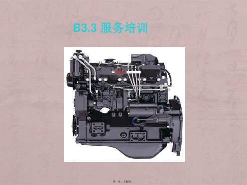
B3.3系列发动机介绍
9、活塞 10、进、排气门 11、摇臂 12、正时齿轮 13、流经机油散热器的冷却液
第十九页,共65页。
润滑系统相关参数
自然进气 涡轮增压
调解阀开启压力
机油容量
490 kPa (71psi) 588 kPa 85psi
总容量 油底壳容量
7.5 Litres
7.0 Litres
8.0 Litres
65 @ 2600RPM 214 @ 1600RPM 自然吸气式 Tier 2
60 @ 2200RPM 214 @ 1600RPM 自然吸气式 Tier 2
▪康明斯B系列3.3升小型工程机械柴油机,由康明斯和小松联合开发,, 60-85马力(45-63千瓦),满足欧美非公路用机动设备第二阶段排放标准 (Tier 2/Stage IIA),广泛应用于小型挖掘机、叉车、发电机组、滑移装载机、空压
典型的排气温度 B 3.3 63Kw @ 2600 RPM. (涡轮增压式)
额定功率下的排气温度 501 C (934F) 全负荷下的排气温度 509 C (948F) (1600RPM)
第九页,共65页。
发动机布置——排气侧 (涡轮增压)
排气岐管 涡轮增压器
发电机 机油滤清器
机油压力传感器 机油尺和涡轮增压回油管
第十页,共65页。
发动机布置——前端 (涡轮增压)
风扇驱动
既可以向前吹也可以向后吹
风扇驱动速比
1.1 正常情况 0.85 要求低噪音的应用 1.24 要求高冷却能力的应用
风扇中心距.
标准 260mm (10.23inch).
可选 355mm (13.97 ")
风扇皮带 1/2 “ or 5/8 ” 单槽V型带
93LC46B中文资料

FEATURES•Single supply with operation down to 2.5V •Low power CMOS technology - 1 mA active current (typical)- 1 µ A standby current (maximum)•128 x 8 bit organization (93LC46A)•64 x 16 bit organization (93LC46B)•Self-timed ERASE and WRITE cycles (including auto-erase)•Automatic ERAL before WRAL•Power on/off data protection circuitry •Industry standard 3-wire serial interface•Device status signal during ERASE/WRITE cycles •Sequential READ function•1,000,000 E/W cycles guaranteed •Data retention > 200 years•8-pin PDIP/SOIC and 8-pin TSSOP packages •Available for the following temperature ranges: DESCRIPTIONThe Microchip T echnology Inc. 93LC46AX/BX are 1K-bit, low voltage serial Electrically Erasable PROMs. The device memory is configured as x8 (93LC46A) or x16 bits (93LC46B). Advanced CMOS technology makes these devices ideal for low power nonvolatile memory applications. The 93LC46AX/BX is available in standard 8-pin DIP , 8-pin surface mount SOIC, and TSSOP packages. The 93LC46AX/BX are offered only in a 150-mil SOIC package.-Commercial (C):0 ° C to +70 ° C -Industrial (I): -40 ° C to +85 °C元器件交易网93LC46A/B1.0ELECTRICALCHARACTERISTICS1.1Maximum Ratings* Vcc...................................................................................7.0V All inputs and outputs w.r.t. Vss ................-0.6V to Vcc +1.0V Storage temperature.....................................-65°C to +150°C Ambient temp. with power applied.................-65°C to +125°C Soldering temperature of leads (10 seconds).............+300°C ESD protection on all pins................................................4 kV*Notice: Stresses above those listed under “Maximum ratings” may cause permanent damage to the device. This is a stress rating only and functional operation of the device at those or any other conditions above those indicated in the operational listings of this specification is not implied. Exposure to maximum rating conditions for extended peri-ods may affect device reliability.TABLE 1-1PIN FUNCTION TABLE Name FunctionCS Chip SelectCLK Serial Data ClockDI Serial Data InputDO Serial Data OutputV SS GroundNC No ConnectV CC Power SupplyTABLE 1-2DC AND AC ELECTRICAL CHARACTERISTICSAll parameters apply over the specified operating ranges unless otherwise noted Commercial (C): V CC = +2.5V to +6.0V Tamb = 0°C to +70°C Industrial (I):V CC = +2.5V to +6.0V Tamb = -40°C to +85°CParameter Symbol Min.Max.Units ConditionsHigh level input voltage V IH1 2.0Vcc +1V 2.7V < V CC≤ 5.5V (Note 2) V IH20.7 V CC Vcc +1V V CC < 2.7VLow level input voltage V IL1-0.30.8V V CC > 2.7V (Note 2) V IL2-0.30.2 Vcc V V CC < 2.7VLow level output voltage V OL1—0.4V I OL = 2.1 mA; Vcc = 4.5VV OL2—0.2V I OL =100 µA; Vcc = Vcc Min.High level output voltage V OH1 2.4—V I OH = -400 µA; Vcc = 4.5VV OH2V CC-0.2—V I OH = -100 µA; Vcc = Vcc Min.Input leakage current I LI-1010µA V IN = V SS to Vcc Output leakage current I LO-1010µA V OUT = V SS to VccPin capacitance (all inputs/outputs)C IN, C OUT—7pFV IN/V OUT = 0 V (Notes 1 & 2)Tamb = +25°C, F CLK = 1 MHzOperating current I CC write— 1.5mAI CC read— 1500mAµAF CLK = 2 MHz; Vcc = 6.0VF CLK = 1 MHz; Vcc = 3.0VStandby current I CCS—1µA CS = VssClock frequency F CLK—21MHzMHzV CC > 4.5VV CC < 4.5VClock high time T CKH250—nsClock low time T CKL250—nsChip select setup time T CSS50—ns Relative to CLK Chip select hold time T CSH0—ns Relative to CLK Chip select low time T CSL250—nsData input setup time T DIS100—ns Relative to CLK Data input hold time T DIH100—ns Relative to CLK Data output delay time T PD—400ns C L = 100 pFData output disable time T CZ—100ns C L = 100 pF (Note 2) Status valid time T SV—500ns C L = 100 pFProgram cycle time T WC—6ms ERASE/WRITE mode T EC—6ms ERAL modeT WL—15ms WRAL modeEndurance—1M—cycles25°C, V CC = 5.0V, Block Mode (Note 3)Note 1:This parameter is tested at T amb = 25°C and Fclk = 1 MHz.2:This parameter is periodically sampled and not 100% tested.3:This application is not tested but guaranteed by characterization. For endurance estimates in a specific application, please consult the Total Endurance Model which may be obtained on Microchip’s BBS or website.元器件交易网93LC46A/B2.0PIN DESCRIPTION2.1Chip Select (CS)A high level selects the device; a low level deselects the device and forces it into standby mode. However, a pro-gramming cycle which is already in progress will be completed, regardless of the Chip Select (CS) input signal. If CS is brought low during a program cycle, the device will go into standby mode as soon as the pro-gramming cycle is completed.CS must be low for 250 ns minimum (T CSL) between consecutive instructions. If CS is low, the internal con-trol logic is held in a RESET status.2.2Serial Clock (CLK)The Serial Clock is used to synchronize the communi-cation between a master device and the 93LC46AX/ BX. Opcodes, address, and data bits are clocked in on the positive edge of CLK. Data bits are also clocked out on the positive edge of CLK.CLK can be stopped anywhere in the transmission sequence (at high or low level) and can be continued anytime with respect to clock high time (T CKH) and clock low time (T CKL). This gives the controlling master freedom in preparing opcode, address, and data.CLK is a “Don't Care” if CS is low (device deselected). If CS is high, but the START condition has not been detected, any number of clock cycles can be received by the device without changing its status (i.e., waiting for a ST ART condition).CLK cycles are not required during the self-timed WRITE (i.e., auto ERASE/WRITE) cycle.After detection of a ST ART condition the specified num-ber of clock cycles (respectively low to high transitions of CLK) must be provided. These clock cycles are required to clock in all required opcode, address, and data bits before an instruction is executed (T able 2-1 and T able 2-2). CLK and DI then become don't care inputs waiting for a new ST ART condition to be detected.2.3Data In (DI)Data In (DI) is used to clock in a ST ART bit, opcode, address, and data synchronously with the CLK input.2.4Data Out (DO)Data Out (DO) is used in the READ mode to output data synchronously with the CLK input (T PD after the posi-tive edge of CLK).This pin also provides READY/BUSY status information during ERASE and WRITE cycles. READY/BUSY sta-tus information is available on the DO pin if CS is brought high after being low for minimum chip select low time (T CSL) and an ERASE or WRITE operation has been initiated.The status signal is not available on DO, if CS is held low during the entire ERASE or WRITE cycle. In this case, DO is in the HIGH-Z mode. If status is checked after the ERASE/WRITE cycle, the data line will be high to indicate the device is ready.TABLE 2-1INSTRUCTION SET FOR 93LC46AInstruction SB Opcode Address Data In Data Out Req. CLK CyclesERASE111A6A5A4A3A2A1A0—(RDY/BSY)10ERAL10010X X X X X—(RDY/BSY)10EWDS10000X X X X X—HIGH-Z10EWEN10011X X X X X—HIGH-Z10READ110A6A5A4A3A2A1A0—D7 - D018WRITE101A6A5A4A3A2A1A0D7 - D0(RDY/BSY)18WRAL10001X X X X X D7 - D0(RDY/BSY)18 TABLE 2-2INSTRUCTION SET FOR 93LC46BInstruction SB Opcode Address Data In Data Out Req. CLK CyclesERASE111A5A4A3A2A1A0—(RDY/BSY)9ERAL10010X X X X—(RDY/BSY)9EWDS10000X X X X—HIGH-Z9EWEN10011X X X X—HIGH-Z9READ110A5A4A3A2A1A0—D15 - D025WRITE101A5A4A3A2A1A0D15 - D0(RDY/BSY)25WRAL10001X X X X D15 - D0(RDY/BSY)25元器件交易网93LC46A/B3.0FUNCTIONAL DESCRIPTION Instructions, addresses, and write data are clocked into the DI pin on the rising edge of the clock (CLK). The DO pin is normally held in a HIGH-Z state except when reading data from the device, or when checking the READY/BUSY status during a programming operation. The READY/BUSY status can be verified during an ERASE/WRITE operation by polling the DO pin; DO low indicates that programming is still in progress, while DO high indicates the device is ready. The DO will enter the HIGH-Z state on the falling edge of the CS.3.1START ConditionThe ST ART bit is detected by the device if CS and DI are both high with respect to the positive edge of CLK for the first time.Before a ST ART condition is detected, CS, CLK, and DI may change in any combination (except to that of a ST ART condition), without resulting in any device oper-ation (ERASE, ERAL, EWDS, EWEN, READ, WRITE, and WRAL). As soon as CS is high, the device is no longer in the standby mode.An instruction following a START condition will only be executed if the required amount of opcodes, addresses, and data bits for any particular instruction is clocked in.After execution of an instruction (i.e., clock in or out of the last required address or data bit) CLK and DI become don't care bits until a new ST ART condition is detected.3.2Data In (DI) and Data Out (DO)It is possible to connect the Data In (DI) and Data Out (DO) pins together. However, with this configuration, if A0 is a logic-high level, it is possible for a “bus conflict”to occur during the “dummy zero” that precedes the READ operation. Under such a condition the voltage level seen at DO is undefined and will depend upon the relative impedances of DO and the signal source driv-ing A0. The higher the current sourcing capability of A0, the higher the voltage at the DO pin.3.3Data ProtectionDuring power-up, all programming modes of operation are inhibited until Vcc has reached a level greater than 2.2V. During power-down, the source data protection circuitry acts to inhibit all programming modes when Vcc has fallen below 2.2V at nominal conditions.The ERASE/WRITE Disable (EWDS) and ERASE/ WRITE Enable (EWDS) commands give additional pro-tection against accidentally programming during nor-mal operation.After power-up, the device is automatically in the EWDS mode. Therefore, an EWEN instruction must be performed before any ERASE or WRITE instruction can be executed.元器件交易网93LC46A/B3.4ERASEThe ERASE instruction forces all data bits of the spec-ified address to the logical “1” state. CS is brought low following the loading of the last address bit. This falling edge of the CS pin initiates the self-timed programming cycle.The DO pin indicates the READY/BUSY status of the device if CS is brought high after a minimum of 250 ns low (T CSL). DO at logical “0” indicates that program-ming is still in progress. DO at logical “1” indicates that the register at the specified address has been erased and the device is ready for another instruction.3.5Erase All (ERAL)The Erase All (ERAL) instruction will erase the entire memory array to the logical “1” state. The ERAL cycle is identical to the ERASE cycle, except for the different opcode. The ERAL cycle is completely self-timed and commences at the falling edge of the CS. Clocking of the CLK pin is not necessary after the device has entered the ERAL cycle.The DO pin indicates the READY/BUSY status of the device, if CS is brought high after a minimum of 250 ns low (T CSL) and before the entire ERAL cycle is com-plete.元器件交易网93LC46A/B3.6ERASE/WRITE Disable and Enable(EWDS/EWEN)The 93LC46A/B powers up in the ERASE/WRITE Dis-able (EWDS) state. All programming modes must be preceded by an ERASE/WRITE Enable (EWEN) instruction. Once the EWEN instruction is executed, programming remains enabled until an EWDS instruc-tion is executed or Vcc is removed from the device. T o protect against accidental data disturbance, the EWDS instruction can be used to disable all ERASE/WRITE functions and should follow all programming opera-tions. Execution of a READ instruction is independent of both the EWEN and EWDS instructions.3.7READThe READ instruction outputs the serial data of the addressed memory location on the DO pin. A dummy zero bit precedes the 8-bit (93LC46A) or 16-bit (93LC46B) output string. The output data bits will toggle on the rising edge of the CLK and are stable after the specified time delay (T PD). Sequential read is possible when CS is held high. The memory data will automati-cally cycle to the next register and output sequentially.FIGURE 3-6:READ TIMING CSCLKDI DO110An•••A0HIGH-Z0Dx•••D0Dx•••D0•••Dx D0元器件交易网93LC46A/B3.8WRITEThe WRITE instruction is followed by 8 bits (93LC46A) or 16 bits (93LC46B) of data which are written into the specified address. After the last data bit is put on the DI pin, the falling edge of CS initiates the self-timed auto-erase and programming cycle.The DO pin indicates the READY/BUSY status of the device, if CS is brought high after a minimum of 250 ns low (T CSL) and before the entire write cycle is complete. DO at logical “0” indicates that programming is still in progress. DO at logical “1” indicates that the register at the specified address has been written with the data specified and the device is ready for another instruc-tion.3.9Write All (WRAL)The Write All (WRAL) instruction will write the entire memory array with the data specified in the command. The WRAL cycle is completely self-timed and com-mences at the falling edge of the CS. Clocking of the CLK pin is not necessary after the device has entered the WRAL cycle. The WRAL command does include an automatic ERAL cycle for the device. Therefore, the WRAL instruction does not require an ERAL instruction but the chip must be in the EWEN status.The DO pin indicates the READY/BUSY status of the device if CS is brought high after a minimum of 250 ns low (T CSL).元器件交易网元器件交易网93LC46A/B Array NOTES:元器件交易网93LC46A/B Array NOTES:元器件交易网93LC46A/B Array NOTES:93LC46A/B93LC46A/B PRODUCT IDENTIFICATION SYSTEMSales and SupportData SheetsProducts supported by a preliminary Data Sheet may have an errata sheet describing minor operational differences and recom-mended workarounds. To determine if an errata sheet exists for a particular device, please contact one of the following:1. Y our local Microchip sales office.2. The Microchip Corporate Literature Center U.S. FAX: (602) 786-7277.3. The Microchip’s Bulletin Board, via your local CompuServe number (CompuServe membership NOT required).元器件交易网AMERICASCorporate OfficeMicrochip Technology Inc.2355 West Chandler Blvd.Chandler, AZ 85224-6199Tel: 602-786-7200 Fax: 602-786-7277 Technical Support: 602 786-7627 Web: AtlantaMicrochip T echnology Inc.500 Sugar Mill Road, Suite 200B Atlanta, GA 30350Tel: 770-640-0034 Fax: 770-640-0307 BostonMicrochip Technology Inc.5 Mount Royal AvenueMarlborough, MA 01752T el: 508-480-9990 Fax: 508-480-8575 ChicagoMicrochip Technology Inc.333 Pierce Road, Suite 180Itasca, IL 60143Tel: 630-285-0071 Fax: 630-285-0075 DallasMicrochip T echnology Inc.14651 Dallas Parkway, Suite 816 Dallas, TX 75240-8809Tel: 972-991-7177 Fax: 972-991-8588 DaytonMicrochip T echnology Inc.Two Prestige Place, Suite 150 Miamisburg, OH 45342Tel: 937-291-1654 Fax: 937-291-9175 Los AngelesMicrochip Technology Inc.18201 Von Karman, Suite 1090Irvine, CA 92612Tel: 714-263-1888 Fax: 714-263-1338 New YorkMicrochip T echnology Inc.150 Motor Parkway, Suite 416 Hauppauge, NY 11788T el: 516-273-5305 Fax: 516-273-5335 San JoseMicrochip Technology Inc.2107 North First Street, Suite 590San Jose, CA 95131T el: 408-436-7950 Fax: 408-436-7955 TorontoMicrochip Technology Inc.5925 Airport Road, Suite 200 Mississauga, Ontario L4V 1W1, Canada Tel: 905-405-6279 Fax: 905-405-6253ASIA/PACIFICHong KongMicrochip Asia PacificRM 3801B, Tower T woMetroplaza223 Hing Fong RoadKwai Fong, N.T., Hong KongTel: 852-2-401-1200 Fax: 852-2-401-3431IndiaMicrochip Technology IndiaNo. 6, Legacy, Convent RoadBangalore 560 025, IndiaT el: 91-80-229-0061 Fax: 91-80-229-0062KoreaMicrochip Technology Korea168-1, Y oungbo Bldg. 3 FloorSamsung-Dong, Kangnam-KuSeoul, KoreaTel: 82-2-554-7200 Fax: 82-2-558-5934ShanghaiMicrochip TechnologyRM 406 Shanghai Golden Bridge Bldg.2077 Y an’an Road West, Hongiao DistrictShanghai, PRC 200335T el: 86-21-6275-5700Fax: 86 21-6275-5060SingaporeMicrochip T echnology TaiwanSingapore Branch200 Middle Road#10-03 Prime CentreSingapore 188980T el: 65-334-8870 Fax: 65-334-8850Taiwan, R.O.CMicrochip Technology Taiwan10F-1C 207Tung Hua North RoadTaipei, Taiwan, ROCT el: 886 2-717-7175 Fax: 886-2-545-0139EUROPEUnited KingdomArizona Microchip Technology Ltd.Unit 6, The CourtyardMeadow Bank, Furlong RoadBourne End, Buckinghamshire SL8 5AJTel: 44-1628-851077 Fax: 44-1628-850259FranceArizona Microchip Technology SARLZone Industrielle de la Bonde2 Rue du Buisson aux Fraises91300 Massy, FranceTel: 33-1-69-53-63-20 Fax: 33-1-69-30-90-79GermanyArizona Microchip Technology GmbHGustav-Heinemann-Ring 125D-81739 Müchen, GermanyTel: 49-89-627-144 0 Fax: 49-89-627-144-44ItalyArizona Microchip Technology SRLCentro Direzionale ColleonePalazzo Taurus 1 V. Le Colleoni 120041 Agrate BrianzaMilan, ItalyTel: 39-39-6899939 Fax: 39-39-6899883JAPANMicrochip Technology Intl. Inc.Benex S-1 6F3-18-20, Shin Y okohamaKohoku-Ku, Y okohamaKanagawa 222 JapanTel: 81-4-5471- 6166 Fax: 81-4-5471-61225/8/97 Printed on recycled paper.元器件交易网。
- 1、下载文档前请自行甄别文档内容的完整性,平台不提供额外的编辑、内容补充、找答案等附加服务。
- 2、"仅部分预览"的文档,不可在线预览部分如存在完整性等问题,可反馈申请退款(可完整预览的文档不适用该条件!)。
- 3、如文档侵犯您的权益,请联系客服反馈,我们会尽快为您处理(人工客服工作时间:9:00-18:30)。
IS93C46BISSI®Copyright © 2003 Integrated Silicon Solution, Inc. All rights reserved. ISSI reserves the right to make changes to this specification and its products at any time without notice. ISSI assumes no liability arising out of the application or use of any information, products or services described herein. Customers are advised to obtain the latest version of this device specification before relying on any published information and before placing orders for products.1,024-BIT SERIAL ELECTRICALLY ERASABLE PROMJULY 2003FUNCTIONAL BLOCK DIAGRAMFEATURES•Industry-standard Microwire Interface —Non-volatile data storage —Low voltage operation: Vcc = 2.5V to 5.5V—Full TTL compatible inputs and outputs —Auto increment for efficient data dump •x16 bit organization•Hardware and software write protection—Defaults to write-disabled state at power-up —Software instructions for write-enable/disable •Enhanced low voltage CMOS E 2PROM technology•Versatile, easy-to-use Interface —Self-timed programming cycle —Automatic erase-before-write —Programming status indicator —Word and chip erasable—Chip select enables power savings •Durable and reliable—40-year data retention after 1M write cycles —1 million write cycles —Unlimited read cycles — Schmitt-trigger inputs•Industrial and Automotive Temperature GradeDESCRIPTIONThe IS93C46B is a low-cost 1kb non-volatile,ISSI ® serial EEPROM. It is fabricated using an enhanced CMOS design and process. The IS93C46B contains power-efficient read/write memory, and organization of 64 words of 16 bits.The IS93C46B is fully backward compatible with IS93C46.An instruction set defines the operation of the devices, including read, write, and mode-enable functions. To protect against inadvertent data modification, all erase and write instructions are accepted only while the device is write-enabled. A selected x16 word can be modified with a single WRITE or ERASE instruction. Additionally, the two instructions WRITE ALL or ERASE ALL can program the entire array. Once a device begins its self-timed program procedure, the data out pin (Dout) can indicate the READY/BUSY status by raising chip select (CS). The self-timed write cycle includes an automatic erase-before-writecapability. The device can output any number of consecutive words using a single READ instruction.2Integrated Silicon Solution, Inc. — — 1-800-379-4774Rev.A IS93C46BISSI®PIN CONFIGURATIONS8-Pin JEDEC SOIC “G”8-Pin JEDEC SOIC “GR”PIN DESCRIPTIONSCS Chip Select SK Serial Data Clock D IN Serial Data Input D OUT Serial Data Output NC Not Connected Vcc Power GNDGroundinstruction begins with a start bit of the logical “1” or HIGH. Following this are the opcode (2 bits),address field (6 bits), and data, if appropriate. The clock signal may be held stable at any moment to suspend the device at its last state, allowing clock-speed flexibility. Upon completion of buscommunication, CS would be pulled LOW. The device then would enter Standby mode if no internal programming is underway.Read (READ)The READ instruction is the only instruction that outputs serial data on the D OUT pin. After the read instruction and address have been decoded, data is transferred from the selected memory register into a serial shift register. (Please note that one logical “0” bit precedes the actual 16-bit output data string.) The output on D OUT changes during the low-to-high transitions of SK (see Figure 3).Low Voltage ReadThe IS93C46B has been designed to ensure that data read operations are reliable in low voltage environments.They provide accurate operation with Vcc as low as 2.5V.Auto Increment Read OperationsIn the interest of memory transfer operation applications,the IS93C46B has been designed to output a continuous stream of memory content in response to a single read operation instruction. To utilize this function, the system asserts a read instruction specifying a start location ad-dress. Once the 16 bits of the addressed register have been clocked out, the data in consecutively higher address locations is output. The address will wrap around continu-ously with CS HIGH until the chip select (CS) control pin is brought LOW . This allows for single instruction data dumps to be executed with a minimum of firmware overhead.ApplicationsThe IS93C46B is very popular in many high-volume applications which require low-power, low-density storage. Applications using this device include industrial controls, networking, and numerous other consumer electronics.Endurance and Data RetentionThe IS93C46B is designed for applications requiring up to 1M programming cycles (WRITE, WRALL, ERASE and ERAL). It provides 40 years of secure data retention without power after the execution of 1M programming cycles.Device OperationsThe IS93C46B is controlled by a set of instructions which are clocked-in serially on the Din pin. Before each low-to-high transition of the clock (SK), the CS pin must have already been raised to HIGH, and the Din value must be stable at either LOW or HIGH. Each12348765CS SK D IN D OUTVCC NC NC GND12348765NC VCC CS SKNC GND D OUT D IN12348765CS SK D IN D OUTVCC NC NC GND(Rotated)8-Pin DIP, 8-Pin TSSOPIS93C46BISSI®Write All (WRALL)The write all (WRALL) instruction programs all registers with the data pattern specified in the instruction. As with the WRITE instruction, the falling edge of CS must occur to initiate the self-timed programming cycle. If CS is then brought HIGH after a minimum wait of 250 ns (t CS ), the D OUT pin indicates the READY/BUSY status of the chip (see Figure 6).Write Disable (WDS)The write disable (WDS) instruction disables all programming capabilities. This protects the entire device against acci-dental modification of data until a WEN instruction is executed. (When Vcc is applied, this part powers up in the write disabled state.) To protect data, a WDS instruction should be executed upon completion of each programming operation.Erase Register (ERASE)After the erase instruction is entered, CS must be brought LOW. The falling edge of CS initiates the self-timed internal programming cycle. Bringing CS HIGH after a minimum of t CS , will cause D OUT to indicate the READ/BUSY status of the chip: a logical “0” indicates programming is still in progress;a logical “1” indicates the erase cycle is complete and the part is ready for another instruction (see Figure 8).Erase All (ERAL)Full chip erase is provided for ease of programming. Erasing the entire chip involves setting all bits in the entire memory array to a logical “1” (see Figure 9).Write Enable (WEN)The write enable (WEN) instruction must be executed before any device programming (WRITE, WRALL,ERASE, and ERAL) can be done. When Vcc is applied,this device powers up in the write disabled state. The device then remains in a write disabled state until a WEN instruction is executed. Thereafter, the device remains enabled until a WDS instruction is executed or until Vcc is removed. (See Figure 4.) (Note: Chip select must remain LOW until Vcc reaches its operational value.)Write (WRITE)The WRITE instruction includes 16 bits of data to be written into the specified register. After the last data bit has been applied to D IN , and before the next rising edge of SK, CS must be brought LOW. If the device is write-enabled, then the falling edge of CS initiates the self-timed programming cycle (see WEN).If CS is brought HIGH, after a minimum wait of 250 ns (5V operation) after the falling edge of CS (t CS ) D OUT will indicate the READY/BUSY status of the chip. Logical “0”means programming is still in progress; logical “1” means the selected register has been written, and the part is ready for another instruction (see Figure 5). The READY/BUSY status will not be available if: a) The CS input goes HIGH after the end of the self-timed programming cycle,t WP ; or b) Simultaneously CS is HIGH, Din is HIGH, and SK goes HIGH, which clears the status flag.INSTRUCTION SET - IS93C46B16-bit OrganizationInstruction Start BitOP Code Address (1)Input DataREAD110(A 5-A 0)—WEN (Write Enable)10011xxxx —WRITE101(A 5-A 0)(D 15-D 0) (2)WRALL (Write All Registers)10001xxxx (D 15-D 0) (2)WDS (Write Disable)10000xxxx —ERASE111(A 5-A 0)—ERAL (Erase All Registers)10010xxxx—Notes:1. x = Don't care bit.2.If input data is not 16 bits exactly, the last 16 bits will be taken as input data.IS93C46B ISSI®ABSOLUTE MAXIMUM RATINGS(1)Symbol Parameter Value UnitV GND Voltage with Respect to GND–0.3 to +6.5VT BIAS Temperature Under Bias (Industrial)–40 to +85°CT BIAS Temperature Under Bias (Automotive)–40 to +125°CT STG Storage Temperature–65 to +150°CNotes:1. Stress greater than those listed under ABSOLUTE MAXIMUM RATINGS may causepermanent damage to the device. This is a stress rating only and functional operation of thedevice at these or any other conditions above those indicated in the operational sections ofthis specification is not implied. Exposure to absolute maximum rating conditions forextended periods may affect reliability.OPERATING RANGERange Ambient Temperature V C CCommercial0°C to +70°C 2.5V to 5.5VIndustrial–40°C to +85°C 2.5V to 5.5VAutomotive–40°C to +125°C 2.7V to 5.5V or 4.5V to 5.5VCAPACITANCESymbol Parameter Conditions Max.UnitC IN Input Capacitance V IN = 0V5pFC OUT Output Capacitance V OUT = 0V5pF4Integrated Silicon Solution, Inc. — — 1-800-379-4774Rev.AIS93C46B ISSI®DC ELECTRICAL CHARACTERISTICST A = 0°C to +70°C for Commercial, –40°C to +85°C for Industrial, and –40°C to +125°C for Automotive.Symbol Parameter Test Conditions Vcc Min.Max.Unit V OL Output LOW Voltage I OL = 100 µA 2.5V to 5.5V—0.2V V OL1Output LOW Voltage I OL = 2.1 mA 4.5V to 5.5V—0.4V V OH Output HIGH Voltage I OH = –100 µA 2.5V to 5.5V V CC – 0.2—V V OH1Output HIGH Voltage I OH = –400 µA 4.5V to 5.5V 2.4—V V IH Input HIGH Voltage 2.5V to 5.5V0.7X V CC V CC+1V4.5V to5.5V0.7X V CC V CC+1V IL Input LOW Voltage 2.5V to 5.5V–0.30.2X V CC V4.5V to5.5V–0.30.8I LI Input Leakage V IN = 0V to V CC (CS, SK,D IN,ORG)0 2.5µA I LO Output Leakage V OUT = 0V to V CC, CS = 0V0 2.5µA N o t e s:Automotive grade devices in this table are tested with Vcc = 2.7V to 5.5V and 4.5V to 5.5V.IS93C46B ISSI®POWER SUPPLY CHARACTERISTICST A = 0°C to +70°C for CommercialSymbol Parameter Test Conditions Vcc Min.Max.UnitI CC1Vcc Read Supply Current CS = V IH, SK = 1 MHz 2.7V—100µACMOS input levels 5.0V—500µAI CC2Vcc Write Supply Current CS = V IH, SK = 1 MHz 2.7V—1mACMOS input levels 5.0V—3mAI SB Standby C urrent CS = V IH, SK = 0V 2.7V—10µA5.0V—30µAPOWER SUPPLY CHARACTERISTICST A = –40°C to +85°C for IndustrialSymbol Parameter Test Conditions Vcc Min.Max.UnitI CC1Vcc Read Supply Current CS = V IH, SK = 1 MHz 2.7V—100µACMOS input levels 5.0V—500µAI CC2Vcc Write Supply Current CS = V IH, SK = 1 MHz 2.7V—1mACMOS input levels 5.0V—3mAI SB Standby C urrent CS = V IH, SK = 0V 2.7V—2µA5.0V—4µAPOWER SUPPLY CHARACTERISTICST A = –40°C to +125°C for AutomotiveSymbol Parameter Test Conditions Vcc Min.Max.UnitI CC1Vcc Read Supply Current CS = V IH, SK = 1 MHz 2.7V—100µACMOS input levels 5.0V—500µAI CC2Vcc Write Supply Current CS = V IH, SK = 1 MHz 2.7V—1mACMOS input levels 5.0V—3mAI SB Standby C urrent CS = V IH, SK = 0V 2.7V—3µA5.0V—8µA6Integrated Silicon Solution, Inc. — — 1-800-379-4774Rev.AIS93C46B ISSI®AC ELECTRICAL CHARACTERISTICST A = T A = 0°C to +70°C for Commercial, –40°C to +85°C for IndustrialSymbol Parameter Test Conditions Vcc Min.Max.Unitf SK SK Clock Frequency 2.5V to 5.5V01Mhz2.7V to 5.5V01Mhz4.5V to5.5V02Mhzt SKH SK HIGH Time 2.5V to 5.5V500—ns2.7V to 5.5V350—ns4.5V to5.5V250—nst SKL SK LOW Time 2.5V to 5.5V500—ns2.7V to 5.5V350—ns4.5V to5.5V250—nst CS Minimum CS LOW Time 2.5V to 5.5V500—ns2.7V to 5.5V250—ns4.5V to5.5V250—nst CSS CS Setup Time Relative to SK 2.5V to 5.5V100—ns2.7V to 5.5V50—ns4.5V to5.5V50—nst DIS Din Setup Time Relative to SK 2.5V to 5.5V100—ns2.7V to 5.5V100—ns4.5V to5.5V100—nst CSH CS Hold Time Relative to SK 2.5V to 5.5V0—ns2.7V to 5.5V0—ns4.5V to5.5V0—nst DIH Din Hold Time Relative to SK 2.5V to 5.5V100—ns2.7V to 5.5V100—ns4.5V to5.5V100—nst PD1Output Delay to “1”AC Test 2.5V to 5.5V—400ns2.7V to 5.5V—350ns4.5V to5.5V—250nst PD0Output Delay to “0”AC Test 2.5V to 5.5V—400ns2.7V to 5.5V—350ns4.5V to5.5V—250nst SV CS to Status Valid AC Test 2.5V to 5.5V—400ns2.7V to 5.5V—250ns4.5V to5.5V—250nst DF CS to Dout in 3-state AC Test, CS=VIL 2.5V to 5.5V—200ns2.7V to 5.5V—200ns4.5V to5.5V—100nst WP Write Cycle Time 2.5V to 5.5V—10ms2.7V to 5.5V—10ms4.5V to5.5V—5msN o t e s:1. C L = 100pFIS93C46B ISSI®AC ELECTRICAL CHARACTERISTICST A = –40°C to +125°C for AutomotiveSymbol Parameter Test Conditions Vcc Min.Max.Unitf SK SK Clock Frequency 2.7V to 5.5V01Mhz4.5V to5.5V02Mhzt SKH SK HIGH Time 2.7V to 5.5V500—ns4.5V to5.5V250—nst SKL SK LOW Time 2.7V to 5.5V500—ns4.5V to5.5V250—nst CS Minimum CS LOW Time 2.7V to 5.5V250—ns4.5V to5.5V250—nst CSS CS Setup Time Relative to SK 2.7V to 5.5V100—ns4.5V to5.5V50—nst DIS Din Setup Time Relative to SK 2.7V to 5.5V100—ns4.5V to5.5V100—nst CSH CS Hold Time Relative to SK 2.7V to 5.5V0—ns4.5V to5.5V0—nst DIH Din Hold Time Relative to SK 2.7V to 5.5V100—ns4.5V to5.5V100—nst PD1Output Delay to “1”AC Test 2.7V to 5.5V—400ns4.5V to5.5V—250nst PD0Output Delay to “0”AC Test 2.7V to 5.5V—400ns4.5V to5.5V—250nst SV CS to Status Valid AC Test 2.7V to 5.5V—250ns4.5V to5.5V—250nst DF CS to Dout in 3-state AC Test, CS=VIL 2.7V to 5.5V—200ns4.5V to5.5V—100nst WP Write Cycle Time 2.7V to 5.5V—10ms4.5V to5.5V—5msN o t e s:1. C L = 100pF8Integrated Silicon Solution, Inc. — — 1-800-379-4774Rev.AIS93C46B ISSI®AC WAVEFORMSFIGURE 2. SYNCHRONOUS DATA TIMINGNotes:To determine address bits An-A0 and data bits Dm-Do, see Instruction Set.IS93C46B ISSI®AC WAVEFORMSFIGURE 4. WRITE ENABLE (WEN) TIMINGNotes:1. After the completion of the instruction (D OUT is in READY status) then it may perform another instruction. If device is in BUSY status(D OUT indicates BUSY status) then attempting to perform another instruction could cause device malfunction.2. To determine address bits A n-A0 and data bits D m-D0, see Instruction Set.10Integrated Silicon Solution, Inc. — — 1-800-379-4774Rev.AIS93C46B ISSI®AC WAVEFORMSFIGURE 6. WRITE ALL (WRALL) TIMINGIntegrated Silicon Solution, Inc. — — 1-800-379-477411 R e v.A07/23/03IS93C46B ISSI®AC WAVEFORMSFIGURE 8. ERASE (REGISTER ERASE) CYCLE TIMINGNote for Figures 8 and 9:After the completion of the instruction (D OUT is in READY status) then it may perform another instruction. If device is in BUSY status (D OUT indicates BUSY status) then attempting to perform another instruction could cause device malfunction.12Integrated Silicon Solution, Inc. — — 1-800-379-4774Rev.A07/23/03IS93C46B ISSI®ORDERING INFORMATIONCommercial: 0ºC to +70ºCSpeed Voltage Range Order Part No.Package1Mhz * 2.5V to 5.5V IS93C46B-3P300-mil Plastic DIPIS93C46B-3G SOIC (rotated) JEDECIS93C46B-3GR SOIC JEDECIS93C46B-3Z169-mil TSSOPORDERING INFORMATIONIndustrial Range: -40ºC to +85ºCSpeed Voltage Range Order Part No.Package1Mhz * 2.5V to 5.5V IS93C46B-3PI300-mil Plastic DIPIS93C46B-3GI SOIC (rotated) JEDECIS93C46B-3GRI SOIC JEDECIS93C46B-3ZI169-mil TSSOPORDERING INFORMATIONAutomotive Range: -40ºC to +125ºCSpeed Voltage Range Order Part No.Package1Mhz * 2.7V to 5.5V IS93C46B-3PA300-mil Plastic DIPIS93C46B-3GRA SOIC JEDEC* The specification allows for higher speed. Please see the AC Charateristics for more information. Integrated Silicon Solution, Inc. — — 1-800-379-477413 R e v.A07/23/03。