UC3906中文资料
UC3902中文资料
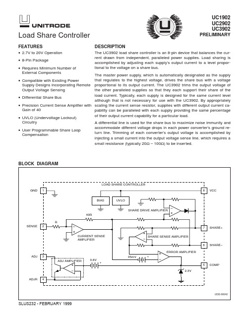
• User Programmable Share Loop Compensation
accommodate different voltage drops in each power converter’s ground return line. Trimming of each converter’s output voltage is accomplished by injecting a small current into the output voltage sense line, which requires a
PARAMETERS
TEST CONDITIONS
MIN TYP MAX UNIT
Share Sense Amplifier
Input Impedance
SHARE+ = 1V, SHARE– = 1V, SENSE = +10mV
10 15
kΩ
200Ω resistor SHARE+ to GND, SHARE– = 1V, SENSE =
PARAMETERS
TEST CONDITIONS
MIN TYP MAX UNIT
Power Supply
Supply Current
SHARE+ = 1V, SENSE = 0V
4
6 mA
VCC = 20V
6
10 mA
Undervoltage Lockout
Startup Voltage
SHARE+ = 0.2V, SENSE = 0V, COMP = 1V
0.12 0.24 0.34 V/µs
2
元器件交易网
UC1902 UC2902 UC3902
UC3909中文资料

DESCRIPTIONThe UC3909family of Switchmode Lead-Acid Battery Chargers accurately controls lead acid battery charging with a highly efficient average current mode control loop.This chip combines charge state logic with average cur-rent PWM control circuitry.Charge state logic commands current or voltage control depending on the charge state.The chip includes undervoltage lockout circuitry to insure sufficient supply voltage is present before output switching starts.Additional circuit blocks include a differential current sense amplifier,a 1.5%voltage reference,a –3.9mV/°C thermistor linearization circuit,voltage and current error amplifiers,a PWM oscillator,a PWM com-parator,a PWM latch,charge state decode bits,and a 100mA open collec-tor output driver.Switchmode Lead-Acid Battery ChargerFEATURES•Accurate and Efficient Control of Battery Charging•Average Current Mode Control from Trickle to Overcharge•Resistor Programmable Charge Currents•Thermistor Interface Tracks Battery Requirements Over Temperature •Output Status Bits Report on Four Internal Charge States•Undervoltage Lockout Monitors VCC and VREFBLOCK DIAGRAMABSOLUTE MAXIMUM RATINGSSupply Voltage (VCC), OUT, STAT0, STAT1. . . . . . . . . . .40V Output Current Sink . . . . . . . . . . . . . . . . . . . . . . . . . . . . . .0.1A CS+, CS-. . . . . . . . . . . . . . . . . . . . . . . . . .-0.4 to VCC (Note 1)Remaining Pin Voltages. . . . . . . . . . . . . . . . . . . . . .-0.3V to 9V Storage Temperature . . . . . . . . . . . . . . . . . . .-65°C to +150°C Junction Temperature . . . . . . . . . . . . . . . . . . .-55°C to +150°C Lead Temperature (Soldering, 10 sec.). . . . . . . . . . . . .+300°CAll currents are positive into,negative out of the specified ter-minal.Consult Packaging Section of Databook for thermal limi-tations and considerations of packages.Note 1:Voltages more negative than -0.4V can be tolerated if current is limited to 50mA.CONNECTION DIAGRAMSELECTRICAL CHARACTERISTICS:Unless otherwise stated these specifications apply for T A = –40°C to +85°C forUC2909; °0C to +70°C for UC3909; C T = 330pF, R SET = 11.5k, R10 = 10k, R THM = 10k, V CC = 15V, Output no load, R STAT0=R STAT1= 10k, CHGENB = OVCTAP = VLOGIC, T A = T J .PARAMETERTEST CONDITIONSMINTYPMAX UNITSCurrent Sense AMP (CSA) Section V ID = CS+ – CS–DC GainCS– = 0, CS+ = -50mV; CS+ = –250mV 4.905 5.10V/V CS+ = 0, CS– = 50mV; CS–- = 250mV 4.9055.10V/V V OFFSET (V CSO – V CAO )CS+ = CS– = 2.3V, CAO = CA–15mV CMRR V CM = –0.25 to VCC – 2, 8.8 < VCC < 1450dB V CM = –0.25 to VCC, 14 < VCC < 3550dB V OL V ID = –550mV, –0.25V < VCM < VCC–2,I O = 500µA0.30.6V V OHV ID = +700mV, –0.25V < VCM < VCC–2,I O = –250µA5.2 5.76.2V Output Source Current V ID = +700mV, CSO = 4V –1–0.5mA Output Sink Current V ID = –550mV, CSO = 1V 3 4.5mA 3dB BandwidthV ID = 90mV, V CM = 0V200kHzELECTRICAL CHARACTERISTICS:Unless otherwise stated these specifications apply for T A= –40°C to +85°C forUC2909; °0C to +70°C for UC3909; C T= 330pF, R SET= 11.5k, R10 = 10k, R THM= 10k, V CC= 15V, Output no load, R STAT0=R STAT1= 10k, CHGENB = OVCTAP = VLOGIC, T A= T J.PARAMETER TEST CONDITIONS MIN TYP MAX UNITS Current Error Amplifier (CEA) SectionI B8.8V < VCC < 35V, V CHGENB= V LOGIC0.10.8µAV IO(Note 2)8.8V < VCC < 35V, CAO = CA–10mVA VO1V < VAO < 4V6090dBGBW T J= 25°C, F = 100kHz1 1.5MHz V OL I O= 250µA0.40.6V V OH I O= –5mA 4.55V Output Source Current CAO = 4V–25–12mA Output Sink Current CAO = 1V23mAI CA–, I TRCK_CONTROL V CHGENB= GND8.51011.5µA Voltage Amplifier (CEA) SectionI B Total Bias Current; Regulating Level0.11µAV IO(Note 2)8.8V < VCC < 35V, VCM = 2.3V, VAO = VA– 1.2mVA VO1V < CAO < 4V6090dBGBW T J= 25°C, F = 100kHz0.250.5MHz V OL I O= 500µA0.40.6V V OH I O= –500µA 4.755 5.25V Output Source Current CAO = 4V–2–1mA Output Sink Current CAO = 1V2 2.5mA VAO Leakage: High Impedance State V CHGENB= GND, STAT0 = 0 & STAT1 = 0,–11µAVAO = 2.3VPulse Width Modulator SectionMaximum Duty Cycle CAO = 0.6V9095100% Modulator Gain CAO = 2.5V, 3.2V637180%/V OSC Peak3V OSC Valley1V Oscillator SectionFrequency8.8V < VCC < 35V198220242kHz Thermistor Derived Reference Section V ID= V RTHM– V R10Initial Accuracy, VAO (RTHM = 10k)V ID= 0, R10 = RTHM =10k (Note 3) 2.2655 2.3 2.3345V2.254 2.3 2.346VV ID= 0, R10 = RTHM =10k, –40°C≤T A< 0°C(Note 3)Line Regulation V CC= 8.8V to 35V310mV VAO RTHM = 138k, R10 = 10k 2.458 2.495 2.532VRTHM = 138k, R10 = 10k, -40°C≤T A< 0°C 2.445 2.495 2.545VRTHM = 33.63k, R10 = 10k 2.362 2.398 2.434VRTHM = 33.63k, R10 = 10k, -40°C≤T A< 0°C 2.350 2.398 2.446VRTHM = 1.014k, R10 = 10k 2.035 2.066 2.097VRTHM = 1.014k, R10 = 10k, -40°C≤T A< 0°C 2.025 2.066 2.107V Charge Enable Comparator Section (CEC)Threshold Voltage As a function of VA–0.991 1.01V/V Input Bias Current CHGENB = 2.3V–0.5–0.1µAELECTRICAL CHARACTERISTICS:Unless otherwise stated these specifications apply for T A= –40°C to +85°C forUC2909; °0C to +70°C for UC3909; C T= 330pF, R SET= 11.5k, R10 = 10k, R THM= 10k, V CC= 15V, Output no load, R STAT0=R STAT1= 10k, CHGENB = OVCTAP = VLOGIC, T A= T J.PARAMETER TEST CONDITIONS MIN TYP MAX UNITS Voltage Sense Comparator Section (VSC)Threshold Voltage STAT0 = 0, STAT1 = 0, Function of V REF0.9450.950.955V/VSTAT0 = 1, STAT1 = 0, Function of V REF0.8950.90.905V/V Over Charge Taper Current Comparator Section (OCTIC)Threshold Voltage Function of 2.3V REF, CA- = CAO0.991 1.01V/V Input Bias Current OVCTAP = 2.3V–0.5–0.1µA Logic 5V Reference Section (VLOGIC)VLOGIC VCC = 15V 4.875 5.0 5.125V Line Regulation8.8V < V CC< 35V315mV Load Regulation0 < I O< 10mA315mV Reference Comparator Turn-on Threshold 4.3 4.8V Short Circuit Current V REF= 0V305080mA Output Stage SectionI SINK Continuous50mAI PEAK100mAV OL I O=50mA1 1.3V Leakage Current V OUT=35V25µA STAT0 & STAT1 Open Collector Outputs SectionMaximum Sink Current V OUT= 8.8V610mA Saturation Voltage I OUT= 5mA0.10.45V Leakage Current V OUT= 35V25µA STATLV Open Collector Outputs SectionMaximum Sink Current V OUT= 5V 2.55mA Saturation Voltage I OUT= 2mA0.10.45V Leakage current V OUT= 5V3µA UVLO SectionTurn-on Threshold 6.87.88.8V Hysteresis100300500mV I CC SectionI CC(run)(See Fig. 1)1319mAI CC(off)VCC = 6.5V2mA Note 2: VIO is measured prior to packaging with internal probe pad.Note 3: Thermistor initial accuracy is measured and trimmed with respect to VAO; VAO = VA–.CA–: The inverting input to the current error amplifier. CAO:The output of the current error amplifier which is internally clamped to approximately4V.It is internally connected to the inverting input of the PWM comparator. CS–,CS+:The inverting and non-inverting inputs to the current sense amplifier.This amplifier has a fixed gain of five and a common-mode voltage range of from–250mV to +VCC.CSO:The output of the current sense amplifier which is internally clamped to approximately 5.7V.CHGENB:The input to a comparator that detects when battery voltage is low and places the charger in a trickle charge state.The charge enable comparator makes the output of the voltage error amplifier a high impedance while forcing a fixed10µA into CA–to set the trickle charge current.PIN DESCRIPTIONSGND :The reference point for the internal reference,all thresholds,and the return for the remainder of the de-vice.The output sink transistor is wired directly to this pin.OVCTAP :The overcharge current taper pin detects when the output current has tapered to the float thresh-old in the overcharge state.OSC :The oscillator ramp pin which has a capacitor (C T )to ground.The ramp oscillates between approximately 1.0V to 3.0V and the frequency is approximated by:frequency C R T SET=••112.OUT :The output of the PWM driver which consists of an open collector output transistor with 100mA sink capabil-ity.R10:Input used to establish a differential voltage corre-sponding to the temperature of the thermistor.Connect a 10k resistor to ground from this point.RSET :A resistor to ground programs the oscillator charge current and the trickle control current for the oscil-lator ramp.The oscillator charge current is approximately175.R SET.The trickle control current (I TRCK_CONTROL )is approxi-mately 0115.R SET .RTHM :A 10k thermistor is connected to ground and is thermally connected to the battery.The resistance will vary exponentially over temperature and its change is used to vary the internal 2.3V reference by –3.9mV/°C.The recommended thermistor for this function is part number L1005-5744-103-D1,Keystone Carbon Com-pany, St. Marys, PA.STAT0:This open collector pin is the first decode bit used to decode the charge states.STAT1:This open collector pin is the second decode bit used to decode the charge states.STATLV :This bit is high when the charger is in the float state.VA–: The inverting input to the voltage error amplifier.VAO :The output of the voltage error amplifier.The up-per output clamp voltage of this amplifier is 5V.VCC :The input voltage to the chip.The chip is opera-tional between 7.5V and 40V and should be bypassed with a 1µF capacitor.A typical I CC vs.temperature is shown in Figure 1.VLOGIC :The precision reference voltage.It should be bypassed with a 0.1µF capacitor.Charge State Decode ChartSTAT0and STAT1are open collector outputs.The out-put is approximately 0.2V for a logic 0.STAT1STAT0Trickle Charge 00Bulk Charge 01Over Charge 10Float Charge11PIN DESCRIPTIONS (cont.)CCAPPLICATION INFORMATIONA Block Diagram of the UC3909is shown on the first page,while a Typical Application Circuit is shown in Fig-ure 2.The circuit in Figure 2requires a DC input voltage between 12V and 40V.The UC3909uses a voltage control loop with average current limiting to precisely control the charge rate of a lead-acid battery.The small increase in complexity of average current limiting is offset by the relative simplicity of the control loop design.CONTROL LOOP Current Sense AmplifierThis amplifier measures the voltage across the sense re-sistor RS with a fixed gain of five and an offset voltage of 2.3V.This voltage is proportional to the battery current.The most positive voltage end of RS is connected to CS-ensuring the correct polarity going into the PWM com-parator.CSO = 2.3V when there is zero battery current.RS is chosen by dividing 350mV by the maximum allow-able load current.A smaller value for RS can be chosen to reduce power dissipation.Maximum Charge Current,Ibulk,is set by knowing the maximum voltage error amplifier output,V OH =5V,the maximum allowable drop across RS,and setting the re-sistors RG1 and RG2 such that;(1)RG RG V VLOGIC CA V V V V VRS RS RS1255523527185=•=•=•=–––...2••I RS BULK The maximum allowable drop across RS is specified to limit the maximum swing at CSO to approximately 2.0V to keep the CSO amplifier output from saturating.No charge/load current: V CSO = 2.3V,Max charge/load current: V max(CSO)= 2.3V–2.0V = 0.3V Voltage Error Amplifier:The voltage error amplifier (VEA) senses the battery voltage and compares it to the 2.3V –3.9mV/°C thermis-tor generated reference.Its output becomes the current command signal and is summed with the current sense amplifier output.A 5.0V voltage error amplifier upper clamp limits maximum load current.During the trickle charge state,the voltage amplifier output is opened (high impedance output)by the charge enable comparator.A trickle bias current is summed into the CA–input which sets the maximum trickle charge current.The VEA,V OH =5V clamp saturates the voltage loop and consequently limits the charge current as stated in Equation 1.During the trickle bias state the maximum allowable charge current (ITC) is similarly determined:(2)ITC I RG RS TRICK CONTROL =••_15I TRCK_CONTROL is the fixed control current into CA–.I TRCK_CONTROL is 10µA when R SET =11.5k.See RSET pin description for equation.Current Error AmplifierThe current error amplifier (CA)compares the output of the current sense amplifier to the output of the voltage error amplifier.The output of the CA forces a PWM duty cycle which results in the correct average battery current.With integral compensation,the CA will have a very high DC current gain,resulting in effectively no average DC current error.For stability purposes,the high frequency gain of the CA must be designed such that the magni-tude of the down slope of the CA output signal is less than or equal to the magnitude of the up slope of the PWM ramp.CHARGE ALGORITHMRefer to Figure 3in UC3906Data Sheet in the data book.A) Trickle Charge StateSTAT0 = STAT1 = STATLV = logic 0When CHGNB is less than VREF (2.3V –3.9mV/°C),STATLV is forced low.This decreases the sense voltage divider ratio, forcing the battery to overcharge (VOC).(3)()VOC VREF RS RS RS RS RS RS =•++()()||123434||During the trickle charge state,the output of the voltage error amplifier is high impedance.The trickle control cur-rent is directed into the CA–pin setting the maximum trickle charge current.The trickle charge current is de-fined in Equation 2.B) Bulk Charge StateSTAT1 = STATLV = logic 0, STAT0 = logic 1As the battery charges,the UC3909will transition from trickle to bulk charge when CHGENB becomes greater than 2.3V. The transition equation is(4)VT VREF RS RS RS RS RS RS RS =•+++(||)(||)1234234STATLV is still driven low.During the bulk charge state,the voltage error amplifier is now operational and is commanding maximum charge current (I BULK )set by Equation 1.The voltage loop at-tempts to force the battery to VOC.C) Overcharge StateSTAT0 = STATLV = logic 0, STAT1 = logic 1The battery voltage surpasses 95%of VOC indicating the UC3909 is in its overcharge state.During the overcharge charge state,the voltage loop be-comes stable and the charge current begins to taper off.As the charge current tapers off,the voltage at CSO in-creases toward its null point of 2.3V.The center connec-tion of the two resistors between CSO and VLOGIC sets the overcurrent taper threshold (OVCTAP).Knowing the desired overcharge terminate current (I OCT ),the resistors R OVC1and R OVC2can be calculated by choosing a value of R OVC2and using the following equation:(5)()R I RS R OVC OCT OVC 1218518=•••.D) Float StateSTAT0 = STAT1 = STATLV = logic 1The battery charge current tapers below its OVCTAP threshold,and forces STATLV high increasing the volt-age sense divider ratio.The voltage loop now forces the battery charger to regulate at its float state voltage (V F ).(6)()()V V RS RS RS RS F REF =++1233If the load drains the battery to less than 90%of V F ,the charger goes back to the bulk charge state, STATE 1.OFF LINE APPLICATIONSFor off line charge applications,either Figure 3or Figure 4can be used as a baseline.Figure 3has the advan-tage of high frequency operation resulting in a small iso-lation transformer.Figure 4is a simpler design,but at the expense of larger magnetics.APPLICATION INFORMATION (cont.)APPLICATION INFORMATION (cont.)UNITRODE CORPORATION7 CONTINENTAL BLVD. • MERRIMACK, NH 03054TEL. (603) 424-2410 • FAX (603) 424-3460IMPORTANT NOTICETexas Instruments and its subsidiaries (TI) reserve the right to make changes to their products or to discontinue any product or service without notice, and advise customers to obtain the latest version of relevant information to verify, before placing orders, that information being relied on is current and complete. All products are sold subject to the terms and conditions of sale supplied at the time of order acknowledgement, including those pertaining to warranty, patent infringement, and limitation of liability.TI warrants performance of its semiconductor products to the specifications applicable at the time of sale in accordance with TI’s standard warranty. Testing and other quality control techniques are utilized to the extent TI deems necessary to support this warranty. Specific testing of all parameters of each device is not necessarily performed, except those mandated by government requirements.CERTAIN APPLICATIONS USING SEMICONDUCTOR PRODUCTS MAY INVOLVE POTENTIAL RISKS OF DEATH, PERSONAL INJURY, OR SEVERE PROPERTY OR ENVIRONMENTAL DAMAGE (“CRITICAL APPLICATIONS”). TI SEMICONDUCTOR PRODUCTS ARE NOT DESIGNED, AUTHORIZED, OR WARRANTED TO BE SUITABLE FOR USE IN LIFE-SUPPORT DEVICES OR SYSTEMS OR OTHER CRITICAL APPLICATIONS. INCLUSION OF TI PRODUCTS IN SUCH APPLICATIONS IS UNDERSTOOD TO BE FULLY AT THE CUSTOMER’S RISK.In order to minimize risks associated with the customer’s applications, adequate design and operating safeguards must be provided by the customer to minimize inherent or procedural hazards.TI assumes no liability for applications assistance or customer product design. TI does not warrant or represent that any license, either express or implied, is granted under any patent right, copyright, mask work right, or other intellectual property right of TI covering or relating to any combination, machine, or process in which such semiconductor products or services might be or are used. TI’s publication of information regarding any third party’s products or services does not constitute TI’s approval, warranty or endorsement thereof.Copyright © 1999, Texas Instruments Incorporated。
PMBT3906中文资料

IMPORTANT NOTICEDear customer,As from October 1st, 2006 Philips Semiconductors has a new trade name-NXP Semiconductors,which will be used in future data sheets together with new contactdetails.In data sheets where the previous Philips references remain,please use the new links asshown below. use use (Internet)sales.addresses@ use salesaddresses@(email)The copyright notice at the bottom of each page (or elsewhere in the document,depending on the version)- © Koninklijke Philips Electronics N.V . (year). All rights reserved -is replaced with:- © NXP B.V . (year). All rights reserved. -If you have any questions related to the data sheet, please contact our nearest salesoffice via e-mail or phone (details via salesaddresses@). Thank you for yourcooperation and understanding,NXP SemiconductorsPMBT3906PNP switching transistorRev. 05 — 4 October 2007Product data sheetPNP switching transistor PMBT3906FEATURES•Collector current capability I C=−200mA •Collector-emitter voltage V CEO=−40V.APPLICATIONS•General amplification and switching.DESCRIPTIONPNP switching transistor in a SOT23 plastic package. NPN complement: PMBT3904.MARKINGNote1.∗=p: Made in Hong Kong.∗=t: Made in Malaysia.∗=W: Made in China.QUICK REFERENCE DATA PINNINGTYPE NUMBER MARKING CODE(1) PMBT3906∗2A SYMBOL PARAMETER MAX.UNIT V CEO collector-emitter voltage−40VI C collector current (DC)−200mAPIN DESCRIPTION1base2emitter3collectorhandbook, halfpage213MAM256Top view231Fig.1 Simplified outline (SOT23) and symbol.ORDERING INFORMATIONTYPE NUMBERPACKAGENAME DESCRIPTION VERSIONPMBT3906−plastic surface mounted package; 3leads SOT23PNP switching transistor PMBT3906LIMITING VALUESIn accordance with the Absolute Maximum Rating System (IEC60134).SYMBOL PARAMETER CONDITIONS MIN.MAX.UNIT V CBO collector-base voltage open emitter−−40VV CEO collector-emitter voltage open base −−40VV EBO emitter-base voltage open collector−−6VI C collector current(DC)−−200mAI CM peak collector current−−200mAI BM peak base current−−100mAP tot total power dissipation T amb≤25°C; note1−250mWT stg storage temperature−65+150°CT j junction temperature−150°CT amb operating ambient temperature−65+150°C Note1.Transistor mounted on an FR4 printed-circuit board.THERMAL CHARACTERISTICSSYMBOL PARAMETER CONDITIONS VALUE UNITR th(j-a)thermal resistance from junction to ambient note1500K/W Note1.Transistor mounted on an FR4 printed-circuit board.PNP switching transistor PMBT3906CHARACTERISTICST amb=25°C unless otherwise specified.SYMBOL PARAMETER CONDITIONS MIN.MAX.UNIT I CBO collector cut-off current I E=0; V CB=−30V−−50nAI EBO emitter cut-off current I C=0; V EB=−6V−−50nAh FE DC current gain V CE=−1V; see Fig.2I C=−0.1mA60−I C=−1mA80−I C=−10mA100300I C=−50mA60−I C=−100mA30−V CEsat collector-emitter saturationvoltage I C=−10mA; I B=−1mA−−250mV I C=−50mA; I B=−5mA−−400mVV BEsat base-emitter saturation voltage I C=−10mA; I B=−1mA−−850mVI C=−50mA; I B=−5mA−−950mV C c collector capacitance I E=i e=0; V CB=−5V;f=1MHz− 4.5pF C e emitter capacitance I C=i c=0; V EB=−500mV;f=1MHz−10pFf T transition frequency I C=−10mA; V CE=−20V;f=100MHz250−MHzF noise figure I C=−100µA; V CE=−5V;R S=1kΩ; f=10Hz to15.7kHz−4dB Switching times (between 10% and 90% levels);see Fig.7t d delay time I Con=−10mA; I Bon=−1mA;I Boff=1mA −35nst r rise time−35ns t s storage time−225ns t f fall time−75nsPNP switching transistor PMBT3906handbook, halfpage 0400600200MHC459−10−1−1−10I C (mA)h FE−102−103(1)(3)(2)Fig.2 DC current gain; typical values.V CE =−1V.(1)T amb =150°C.(2)T amb =25°C.(3)T amb =−55°C.handbook, halfpage 0−10−2500−50−100−150−200−2V CE (V)I C (mA)−4−6−8MHC460(1)(2)(3)(9)(7)(10)(8)(6)(5)(4)Fig.3Collector current as a function of collector-emitter voltage.(1)I B =−1.5mA.(2)I B =−1.35mA.(3)I B =−1.2mA.(4)I B =−1.05mA.(5)I B =−0.9mA.(6)I B =−0.75mA.(7)I B =−0.6mA.(8)I B =−0.45mA.(9)I B =−0.3mA.(10)I B =−0.15mA.T amb =25°C.handbook, halfpage −200−1200−400−600−800−1000MHC461−1−10−1I C (mA)V BE(mV)−10−102−103(3)(2)(1)Fig.4Base-emitter voltage as a function ofcollector current.V CE =−1V.(1)T amb =−55°C.(2)T amb =25°C.(3)T amb =150°C.handbook, halfpage −200−1200−400−600−800−1000MHC462−1−10−1I C (mA)V BEsat (mV)−10−102−103(1)(3)(2)Fig.5Base-emitter saturation voltage as a function of collector current.I C /I B =10.(1)T amb =−55°C.(2)T amb =25°C.(3)T amb =150°C.PNP switching transistor PMBT3906handbook, halfpage −103−102−10MHC463−10−1−1−10I C (mA)V CEsat(mV)−102−103(1)(2)(3)Fig.6Collector-emitter saturation voltage as afunction of collector current.I C /I B =10.(1)T amb =25°C.(2)T amb =150°C.(3)T amb =−55°C.handbook, full pagewidth R C R2R1DUTMGD624V o R B(probe)450 Ω(probe)450 Ωoscilloscopeoscilloscope V BB V iV CCFig.7 Test circuit for switching times.V i =5V; T =500µs; t p =10µs; t r =t f ≤3ns.R1=56Ω; R2=2.5k Ω; R B =3.9k Ω; R C =270Ω.V BB =1.9V; V CC =−3V.Oscilloscope: input impedance Z i =50Ω.PNP switching transistorPMBT3906PACKAGE OUTLINE UNITA 1max.b p c D E e 1H E L p Q w v REFERENCES OUTLINEVERSIONEUROPEAN PROJECTION ISSUE DATE 97-02-2899-09-13IEC JEDEC EIAJ mm 0.10.480.380.150.09 3.02.8 1.41.20.95e 1.9 2.52.10.550.450.10.2DIMENSIONS (mm are the original dimensions)0.450.15 SOT23TO-236AB b p D e 1e AA 1L p Qdetail X H E E w M v M AB A B 012 mmscale A 1.10.9cX123Plastic surface mounted package; 3 leads SOT23Legal informationData sheet status[1]Please consult the most recently issued document before initiating or completing a design.[2]The term ‘short data sheet’ is explained in section “Definitions”.[3]The product status of device(s)described in this document may have changed since this document was published and may differ in case of multiple devices.The latest product statusinformation is available on the Internet at URL .DefinitionsDraft —The document is a draft version only. The content is still underinternal review and subject to formal approval, which may result inmodifications or additions. NXP Semiconductors does not give anyrepresentations or warranties as to the accuracy or completeness ofinformation included herein and shall have no liability for the consequences ofuse of such information.Short data sheet —A short data sheet is an extract from a full data sheetwith the same product type number(s)and title.A short data sheet is intendedfor quick reference only and should not be relied upon to contain detailed andfull information. For detailed and full information see the relevant full datasheet, which is available on request via the local NXP Semiconductors salesoffice. In case of any inconsistency or conflict with the short data sheet, thefull data sheet shall prevail.Disclaimers General —Information in this document is believed to be accurate and reliable.However,NXP Semiconductors does not give any representations or warranties,expressed or implied,as to the accuracy or completeness of such information and shall have no liability for the consequences of use of such information.Right to make changes —NXP Semiconductors reserves the right to make changes to information published in this document, including withoutlimitation specifications and product descriptions, at any time and withoutnotice.This document supersedes and replaces all information supplied priorto the publication hereof.Suitability for use —NXP Semiconductors products are not designed,authorized or warranted to be suitable for use in medical, military, aircraft,space or life support equipment, nor in applications where failure or malfunction of a NXP Semiconductors product can reasonably be expected to result in personal injury, death or severe property or environmental damage.NXP Semiconductors accepts no liability for inclusion and/or use of NXP Semiconductors products in such equipment or applications and therefore such inclusion and/or use is at the customer’s own risk.Applications —Applications that are described herein for any of these products are for illustrative purposes only. NXP Semiconductors makes no representation or warranty that such applications will be suitable for the specified use without further testing or modification.Limiting values —Stress above one or more limiting values (as defined in the Absolute Maximum Ratings System of IEC 60134)may cause permanent damage to the device.Limiting values are stress ratings only and operation of the device at these or any other conditions above those given in the Characteristics sections of this document is not implied. Exposure to limiting values for extended periods may affect device reliability.Terms and conditions of sale —NXP Semiconductors products are soldsubject to the general terms and conditions of commercial sale,as publishedat /profile/terms , including those pertaining to warranty,intellectual property rights infringement and limitation of liability, unlessexplicitly otherwise agreed to in writing by NXP Semiconductors. In case ofany inconsistency or conflict between information in this document and suchterms and conditions, the latter will prevail.No offer to sell or license —Nothing in this document may be interpretedor construed as an offer to sell products that is open for acceptance or thegrant,conveyance or implication of any license under any copyrights,patentsor other industrial or intellectual property rights.Trademarks Notice:All referenced brands,product names,service names and trademarks are the property of their respective owners.Contact informationFor additional information, please visit:For sales office addresses, send an email to:salesaddresses@ Document status [1][2]Product status [3]Definition Objective [short] data sheetDevelopment This document contains data from the objective specification for product development.Preliminary [short] data sheetQualification This document contains data from the preliminary specification.Product [short] data sheetProduction This document contains the product specification.© NXP B.V .2007.All rights reserved.For more information, please visit: For sales office addresses, please send an email to: salesaddresses@Date of release: 4 October 2007Document identifier: PMBT3906_N_5Please be aware that important notices concerning this document and the product(s)described herein, have been included in section ‘Legal information’.Revision historyTable 1.Revision history Document ID Release date Data sheet status Change notice Supersedes PMBT3906_N_520071004Product data sheet -PMBT3906_4Modifications:•Marking code corrected (page 2)PMBT3906_4(939775012535)20040121Product specification-PMBT3906_3PMBT3906_3(939775005816)19990427Product specification-PMBT3906_2PMBT3906_CNV_2(939775002091)19970505Product specification --。
UC3906应用电路(摘自电子发烧友)

UC3906应用电路(摘自电子发烧友)
图为环境参数测试仪蓄电池充电器的实际应用电路。
其中,电池额定电压为12V,容量为7Ah,VIN=18V,VF=13.8V,VOC=15V,Imax=500mA,IOCT=50mA。
由于充电器始终接在蓄电池上,为防止蓄电池电流倒流入充电器,在串联调整管与输出端之间串入一只二极管。
同时,为了避免输入电源中断后,蓄电池通过分压电阻R1、R2、R3放电,使R3通过电源指示晶体管(脚7)接地。
图3 12V密封铅酸电池双电平浮充充电器电路图
18V输入电压加入后,Q1导通,开始恒流充电,充电电流为500mA,电池电压逐渐升高。
当电池电压达到过充电压VOC的95%(即14.25V)时,电池转入过充电状态,充电电压维持在过充电电压,充电电流开始下降。
当充电电流降到过充电终止电流(IOCT)时,UC3906的脚10输出高电平,比较器LM339输出低电平,蓄电池自动转入浮充状态。
同时充足电指示发光管发光,指示蓄电池已充足电。
DMMT3906中文资料

Notes:1.Built with adjacent die from a single wafer.2.Device mounted on FR5 PCB: 1.0 x 0.75 x 0.62 in.; pad layout as shown on suggested pad layout document AP02001, which can be found on our website at /datasheets/ap02001.pdf.3.For Packaging Details, go to our website at /datasheets/ap02007.pdf.Marking InformationFeaturesMaximum Ratings@ T A = 25°C unless otherwise specifiedMechanical Data·Case: SOT-26, Molded Plastic·Case Material - UL Flammability Rating Classification 94V-0·Terminals: Solderable per MIL-STD-202,Method 208·Terminal Connections: See Diagram ·Marking: K3Q·Weight: 0.015 grams (approx.)·Ordering Information: See BelowDMMT3906MATCHED PNP SMALL SIGNAL SURFACE MOUNT TRANSISTORN E W P R O DU CTDate Code KeyK3Q = Product Type Marking Code YM = Date Code Marking Y = Year ex: N = 2002M = Month ex: 9 = September(Note 3)Ordering Information·Epitaxial Planar Die Construction·Intrinsically Matched PNP Pair (Note 1)·Small Surface Mount Package ·2% h FE Matched Tolerance·1% h FE Matched Tolerance On RequestElectrical Characteristics@ T A = 25°C unless otherwise specifiedNotes:4.Short duration test pulse used to minimize self-heating effect.5. The DC current gain, h FE , is matched at I C = -10mA and V CE = -1.0V with typical matched tolerances of 1% and maximum of 2%.N E W P R O D U C T0.50.60.70.80.91.0110100V ,B A S E -E M I T T E R (V )S A T U R A T I O N V O L T A G EB E (S A T )I ,COLLECTOR CURRENT (mA)Fig.5,Typical Base-EmitterSaturation Voltage vs.Collector CurrentC1011101001000V ,C O L L E C T O R -E M I T T E R (V )S A T U R A T I O N V O L T A G EC E (S A T )I ,COLLECTOR CURRENT (mA)Fig.4,Typical Collector-Emitter Saturation Voltagevs.Collector CurrentC11010001000.11101000100h ,D C C U R R E N T G A I NF E I ,COLLECTOR CURRENT (mA)Fig.3,Typical DC Current Gain vsCollector CurrentC100100.1110100C ,I N P U T C A P A C I T A N C E (p F )C ,O U T P U T C A P A C I T A N C E (p F )I B O OB O V ,COLLECTOR-BASE VOLTAGE (V)Fig.2,Input and Output Capacitance vs.Collector-Base VoltageCB 050100255075100125150175200P ,P O W E R D I S S I P A T I O N (m W )D T ,AMBIENT TEMPERATURE (°C)Fig.1,Max Power Dissipation vsAmbient TemperatureA 1502002503003500N E W P R O D U C T。
UC3906铅酸蓄电池充电管理芯片

UC3906铅酸蓄电池充电管理芯片
UC3906铅酸蓄电池充电管理芯片
UC3906为阀控密封铅酸蓄电池充电管理芯片,该芯片整合必要的电路,只须少数的外部元件配置,即可提供对密封式铅酸电池充电所需的控制与检测功能,并提供最佳化的充电参数控制,确保电池的使用寿命与工作效能。
图1UC3906外形和引脚功能
UC3906有SOIC-16表面安装(见图1)以及DIP16直插两种封装,它的内部电路原理框图如图2所示。
图2UC3906内部电路原理框图
UC3906内部集成了实现阀控密封铅酸蓄电池最佳充电所需的3种充电逻辑控制和检测功能,并具有环境温度自适应、充放电程度自适应以及限流、欠压保护功能。
其采用的温度补偿技术可使各种充电转换电压随阀控密封铅酸蓄电池电压温度系数的变化而变化,使阀控密封铅酸蓄电池在很宽的温度范围内都能达到最佳充电状态。
KST3906MTF;中文规格书,Datasheet资料

KST3906 — PNP Epitaxial Silicon Transistor© 2010 Fairchild Semiconductor Corporation September 2010KST3906PNP Epitaxial Silicon TransistorFeatures•General Purpose TransistorAbsolute Maximum Ratings T a = 25°C unless otherwise notedElectrical Characteristics T a =25°C unless otherwise noted*Pulse Test: Pulse Width ≤300μs, Duty Cycle ≤2%SymbolParameterValueUnitV CBO Collector-Base Voltage -40V V CEO Collector-Emitter Voltage -40V V EBO Emitter-Base Voltage -5V I C Collector Current-200mA P C Collector Power Dissipation 350mW T STGStorage Temperature150°CSymbolParameterTest Condition Min.Max.UnitBV CBO Collector-Base Breakdown Voltage I C = -10μA, I E =0-40V BV CEO * Collector-Emitter Breakdown Voltage I C = -1.0mA, I B =0-40V BV EBO Emitter-Base Breakdown Voltage I E = -10μA, I C =0-5V I CEX Collector Cut-off Current V CE = -30V, V EB = -3V -50nAh FE* DC Current GainV CE = -1V, I C = -0.1mA V CE = -1V, I C = -1mA V CE = -1V, I C = -10mA V CE = -1V, I C = -50mA V CE = -1V, I C = -100mA60801006030300V CE (sat)* Collector-Emitter Saturation Voltage I C = -10mA, I B = -1.0mAI C = -50mA, I B = -5.0mA -0.25-0.4V V V BE (sat)* Base-Emitter Saturation VoltageI C = -10mA, I B = -1.0mA I C = -50mA, I B = -5.0mA-0.65-0.85-0.95V V f TCurrent Gain Bandwidth Product I C = -10mA, V CE = -20V, f=100MHz 250MHz C obOutput Capacitance V CB = -5V, I E =0, f=1.0MHz 4.5pF NF Noise Figure I C = -100μA, V CE = -5VR S =1K Ω, f=10Hz to 15.7KHz4dB t ONTurn On Time V CC = -3V, V BE = -0.5V I C = -10mA, I B1= -1mA70ns t OFFTurn Off Time V CC = -3V, I C = -10mA I B1=I B2= -1mA300ns1. Base2. Emitter3. CollectorSOT-231232AMarkingKST3906 — PNP Epitaxial Silicon TransistorKST3906 — PNP Epitaxial Silicon TransistorThe following includes registered and unregistered trademarks and service marks, owned by Fairchild Semiconductor and/or its global subsidiaries, and is notAccuPower¥Auto-SPM¥Build it Now¥CorePLUS¥CorePOWER¥CROSSVOLT¥CTL¥Current Transfer Logic¥DEUXPEED®Dual Cool™ EcoSPARK®EfficientMax¥ESBC¥®Fairchild®Fairchild Semiconductor®FACT Quiet Series¥FACT®FAST®FastvCore¥FETBench¥FlashWriter®*FPS¥F-PFS¥FRFET®Global Power Resource SMGreen FPS¥Green FPS¥ e-Series¥G max¥GTO¥IntelliMAX¥ISOPLANAR¥MegaBuck¥MICROCOUPLER¥MicroFET¥MicroPak¥MicroPak2¥MillerDrive¥MotionMax¥Motion-SPM¥OptoHiT™OPTOLOGIC®OPTOPLANAR®®PDP SPM™Power-SPM¥PowerTrench®PowerXS™Programmable Active Droop¥QFET®QS¥Quiet Series¥RapidConfigure¥¥Saving our world, 1mW/W/kW at a time™SignalWise¥SmartMax¥SMART START¥SPM®STEALTH¥SuperFET¥SuperSOT¥-3SuperSOT¥-6SuperSOT¥-8SupreMOS®SyncFET¥Sync-Lock™®*The Power Franchise®TinyBoost¥TinyBuck¥TinyCalc¥TinyLogic®TINYOPTO¥TinyPower¥TinyPWM¥TinyWire¥TriFault Detect¥TRUECURRENT¥*P SerDes¥UHC®Ultra FRFET¥UniFET¥VCX¥VisualMax¥XS™* Trademarks of System General Corporation, used under license by Fairchild Semiconductor.DISCLAIMERFAIRCHILD SEMICONDUCTOR RESERVES THE RIGHT TO MAKE CHANGES WITHOUT FURTHER NOTICE TO ANY PRODUCTS HEREIN TO IMPROVE RELIABILITY, FUNCTION, OR DESIGN. FAIRCHILD DOES NOT ASSUME ANY LIABILITY ARISING OUT OF THE APPLICATION OR USE OF ANY PRODUCT OR CIRCUIT DESCRIBED HEREIN; NEITHER DOES IT CONVEY ANY LICENSE UNDER ITS PATENT RIGHTS, NOR THE RIGHTS OF OTHERS. THESE SPECIFICATIONS DO NOT EXPAND THE TERMS OF FAIRCHILD’S WORLDWIDE TERMS AND CONDITIONS, SPECIFICALLY THE WARRANTY THEREIN, WHICH COVERS THESE PRODUCTS.LIFE SUPPORT POLICYFAIRCHILD’S PRODUCTS ARE NOT AUTHORIZED FOR USE AS CRITICAL COMPONENTS IN LIFE SUPPORT DEVICES OR SYSTEMS WITHOUT THE EXPRESS WRITTEN APPROVAL OF FAIRCHILD SEMICONDUCTOR CORPORATION.As used herein:1. Life support devices or systems are devices or systems which, (a) areintended for surgical implant into the body or (b) support or sustain life, and (c) whose failure to perform when properly used in accordance with instructions for use provided in the labeling, can be reasonably expected to result in a significant injury of the user. 2. A critical component in any component of a life support, device, orsystem whose failure to perform can be reasonably expected to cause the failure of the life support device or system, or to affect its safety or effectiveness.ANTI-COUNTERFEITING POLICYFairchild Semiconductor Corporation's Anti-Counterfeiting Policy. Fairchild's Anti-Counterfeiting Policy is also stated on our external website, , under Sales Support.Counterfeiting of semiconductor parts is a growing problem in the industry. All manufacturers of semiconductor products are experiencing counterfeiting of their parts. Customers who inadvertently purchase counterfeit parts experience many problems such as loss of brand reputation, substandard performance, failed applications, and increased cost of production and manufacturing delays. Fairchild is taking strong measures to protect ourselves and our customers from the proliferation of counterfeit parts. Fairchild strongly encourages customers to purchase Fairchild parts either directly from Fairchild or from Authorized Fairchild Distributors who are listed by country on our web page cited above. Products customers buy either from Fairchild directly or from Authorized Fairchild Distributors are genuine parts, have full traceability, meet Fairchild's quality standards for handling and storage and provide access to Fairchild's full range of up-to-date technical and product information. Fairchild and our Authorized Distributors will stand behind all warranties and will appropriately address any warranty issues that may arise. Fairchild will not provide any warranty coverage or other assistance for parts bought from Unauthorized Sources. Fairchild is committed to combat this global problem and encourage our customers to do their part in stopping this practice by buying direct or from authorized distributors.PRODUCT STATUS DEFINITIONSDefinition of TermsDatasheet Identification Product Status Definition分销商库存信息: FAIRCHILDKST3906MTF。
公交自动报站系统的设计
电子科技大学公交自动报站系统的设计综合课程设计项目姓名:郭昱瑞学号:20100730100132013/6/11目录1.引言 (2)2.设计方案 (3)3.硬件电路设计 (4)3.1.无线通信电路3.2.车载控制电路3.3.车载语音电路3.4.车载显示电路3.5.车载显示电路4.软件程序设计 (7)5.结束语 (8)6.心得体会 (8)摘要:当前国内主要大城市的公交车大都采用人工报站,即每到一站由司机或者乘务员来进行报站。
但有时由于受到各种因素如雨雪天路滑、车上拥挤、乘务员心情的变化等的影响,会出现报错站,漏报站的情况,给乘客特别是不熟悉本市地形的乘客带来了不必要的麻烦,从而影响到了一个城市的窗口形象工程建设。
于是开发研制自动报站系统成为必然。
随着无线通信技术的迅猛发展,各种无线通信设备已广泛应用于通信、金融、交通等领域。
本设计基于射频原理和光伏技术,' 以单片机为核心实现公交线路的自动报站。
与传统报站系统相比,该系统可以实时准确地提供交通信息,有效减少漏报、错报并大大降低司机的工作量,符合当今节能环保的理念,必将带来良好的经济和社会效益。
1.引言公交系统以其运载量大、运送效率高、运输成本低、相对污染小等优点,已被世界各国公认为解决大、中城市交通问题的最佳策略,也是城市赖以生存的重要基础设施之一。
近年来,随着城市公交事业的迅速发展,国内公交线路的报站方式已由传统的售票员报站发展为司机按键报站,但由于司机身兼数职还需完成开关车门等工作,所以经常出现报站不及时或错报、漏报等现象,而且司机在驾驶过程中进行报站也存在一定的安全隐患。
鉴于目前国内公交报站设备的现状,公交报站方式的自动化已势在必行。
随着公交优先战略的确定,公交在缓解城市交通拥堵方面的作用将越来越重要,与这种要求相比,我国大城市公共交通还有很大差距,主要表现为:为社会提供服务信息的水平低,只能是以经验为主的被动、滞后的实施服务,仍以人工作业为主。
- 1、下载文档前请自行甄别文档内容的完整性,平台不提供额外的编辑、内容补充、找答案等附加服务。
- 2、"仅部分预览"的文档,不可在线预览部分如存在完整性等问题,可反馈申请退款(可完整预览的文档不适用该条件!)。
- 3、如文档侵犯您的权益,请联系客服反馈,我们会尽快为您处理(人工客服工作时间:9:00-18:30)。
UC2906/3906铅酸蓄电池充电器
UC3906作为密封铅酸蓄电池充电专用控制集成电路芯片,能够提供三种充
电逻辑状态(大电流充电、可控过充电和浮充充电)控制,能使充电器的充电电压随电池电压温度系数的变化而变化。
从而使密封铅酸蓄电池在很宽的温度范围内达到最佳充电状态(如电池容量和使用寿命),可分别对充电电流、充
电电压(通过电压&电流控制环)实现控制,具有静态工作功耗低的优点,提供实现密封铅酸蓄电池最佳充电所需的控制和检测功能。
UC3906含有独立的电压控制电路和限电流放大器,可以控制UC3906内的驱动器输出,从而达到控制充电电流大小的目的。
驱动器输出电流高达25m
A,可直接驱动外接串联调整管,从而调整充电器的输出电压和电流。
UC3906
内的电压和电流控制比较器用于检测电池的充电状态,并控制充电状态逻辑电路的相应输出信号。
其他特性还包括一种当输入供电电压丢失时,输入提供欠压检测电路与逻辑的输出指示。
另外过充电可以通过过充电指示输出引脚和过充电终止输入引脚被外围电路检测和终止。
最大额定参数
供电电压(+Vin) (40V)
集电极开路输出电压 (40V)
放大器与比较强输入电压…………………………...-0.3V~+40V
过充电终止输入电压………………………………...-0.3V~+40V
电流检测放大器输出电流…………………………………..80mA
别的集电极开路输出电压…………………………………..20mA
关于Vin的涓流差分电压…………………………………….-32V
涓流输出电流. . . . . . . . . . . . . . . . . . . . -40mA
驱动电流 . . . . . . . . . . . . . . . . . . . . . . . . . . . . . . . 80mA
功耗 at TA = 25°C(Note 2) . . . . . . . . 1000mW
功耗 at TC = 25°C (Note 2) . . . . . . . . 2000mW
工作温度. . . . . . . . -55°C to +150°C
存储温度 . . . . . . . . . . . . . . . . . -65°C to +150°C
引脚温度 (Soldering, 10 Seconds) . . . . . . . 300°C
引脚功能:
PIN1: 充电电流控制环路的充电电流检测放大器的输出引脚;
PIN2: 充电电流检测放大器的充电电流检测反相信号输入引脚;
PIN3: 充电电流检测放大器的充电电流检测同相信号输入引脚;
PIN4: 充电电流限电流放大器的反相检测信号输入引脚;
PIN5: UC3906供电输入引脚;
PIN6: UC3906地;
PIN7:充电器电路的电源指示引脚;
PIN8:电池过充电终止控制信号输入引脚;
PIN9:电池过充电指示控制信号输入引脚;
PIN10:充电器电池充电状态电平控制信号输出引脚;
PIN11:充电使能比较器的输出涓电流充电偏置控制信号输出引脚;PIN12:充电使能比较器的控制信号输入引脚;
PIN13:充电电压控制环路的充电电压检测放大器的控制信号输入引脚;PIN14:补偿元件接入引脚;
PIN15:驱动放大器的发射机输出引脚;
PIN16:驱动放大器的集电极输出引脚;
电特性
内部温度特性和公差
操作与应用信息
图1显示为UC3906的双电平浮充电路
通过DRIVER驱动一个外部PNP三极管来控制大电流充电。
当被充电电池电压或温度过低时,充电使能比较器控制充电器进入涓流充电状态。
当UC3906内
的驱动器截止,充电器电路还能输出涓流充电电流。
当被充电电池短路或反接时,充电器只能小电流充电,避免了因为充电电流过大而损坏电池。
利用内部的使能比较器的涓流充电控制偏置输出引脚输出的信号可以在被充电电池短路时,使充电器电路输出的电流很小,从而保护充电器电路。
当充电器的输入供
电电压偏低或电池过充电,UC3906都能加以指示并输出终止电池过充电控制信
号。
图2显示了充电器的状态图。
低压检测电路使充电进入状态1,在这种状态下,一旦使阈值被超过,充电器将提供一个被电流检测电阻Rs控制的峰值电流(R s上的压降为0.25V)
在充电状态1和充电状态2,为确保电池充足电,UC3906内的电压控制环设置了一个更高的电池电压设定值Voc。
当电池电压达到Voc的95%时,充电电路进入充电工作状态2(过充电状态),直到UC3906的过充电终止引脚的电位变为高电平。
在图1中,利用UC3906内的电流检测放大器来检测电池充电电流的大小,可以确保电池充电电流减小到指定的Ioct。
通过使用UC3906的PIN9引脚
输出的过充电指示信号,采用如定时器等类似电路,可以控制被充电电池的过充电。
如果这个电池接上放电负载,电池开始放电,该充电电路将它所有输出
提供给负载。
当电池电压低于浮充电压的90%时,充电电路又进入充电状态1。
当去掉负载后,将进入一个完整的充电过程。
图3显示了一个完整的充电、放电的双电平浮充图表
图2. 双电平浮充图标和计算公式
说明:VT:溃电电压(涓流充电阈值电压)
VF:浮充电压VOC:过充电压
图3.典型充电流程:双电平浮充
图3工作流程说明:充电电路在刚一接通电源的时间内,是以涓流电流为电池充电,当电池电压达到VT时,充电逻辑控制电路关断涓流充电,转为大电流充电。
当电池电压达到V12时,表示充电电路进入过充状态,当电池电压达到过充电压VOC时,充电电流开始减小。
当充电电流减小到Ioct时,充电电流检测放大器输出信号加到过充电终止控制引脚的电平变高,充电电路改为浮充充电,并却维持充电电池电压为VF。
这时如果电池加上放电负载并开始以恒定的电流放电,当电池的放电电压低于V31时,充电电路又开始为电池充电,进入状态1,,开始一个新的充电周期。
匹配电池需求的补偿参考基准
当充电器进入浮充状态,电池将会维持在一个精确的浮充电压VF。
在大电流和过充快速充电后这种浮充电压的准确性可以使电池寿命最大化。
UC3906所
有的电压阈值来自内部补偿参考基准。
其基准电压大小可以随环境温度变化而变化,并却变化规律与铅酸蓄电池充电电压的温度特性一致。
即使在极端温度下,也可以进一步保证最佳充电。
双阶跃电流充电操作
如图4,5和6举例说明了UC3906的另一种充电方案。
双阶跃电流充电对于大容量电池充电是非常有用的。
一个持续电流充电状态,保证充电电荷平均分布在每个电池格,持续电流充电状态相当于浮充状态(除了V12电压到达时的情况)。
没有过充状态。
因为PIN8始终是高电平。
电流检测放大器用来调整持续电流。
在大多数应用中,输出电流检测用电阻和外部晶体管保障,同时避免UC3906产生较高的功耗。
输入与输出间串联一个PNP三极管
UC3906使用时最好在输入与输出间串联一个三极管。
尽管UC3906内部有一个N PN输出用三极管,但图1和图4中都使用了一个PNP串联三极管。
输入到输出仅需一个串联二极管和、电流检测电阻和使用在饱和状态下的PNP三极管。
这个
串联二极管在大部分应用中可不要,这个二极管可在无输入情况下防止电池反充。
在无充电电源输入时,为了反充发生的最小可能性,可以把电阻分压器接
到PIN7来代替接地。
新推出的UC3909的特点:
1.四阶段控制,增加了一个蓄电池激活修复功能,电池电压低于10V时,U C3906是不会充电的。
而UC3909可以小电流充电,待电池电压上升到10 V后,在开始三阶段式充电。
2.PWM控制MOS,效率高。
3.因为是PWM控制,所有充电电流是有波形的,相应的支持“平均充电电流检测”(类似有效值测量)。